CN110069934B - Memory storage system, host system verification method and memory storage device - Google Patents
Memory storage system, host system verification method and memory storage deviceDownload PDFInfo
- Publication number
- CN110069934B CN110069934BCN201810062088.8ACN201810062088ACN110069934BCN 110069934 BCN110069934 BCN 110069934BCN 201810062088 ACN201810062088 ACN 201810062088ACN 110069934 BCN110069934 BCN 110069934B
- Authority
- CN
- China
- Prior art keywords
- host system
- information
- memory storage
- storage device
- authentication
- Prior art date
- Legal status (The legal status is an assumption and is not a legal conclusion. Google has not performed a legal analysis and makes no representation as to the accuracy of the status listed.)
- Active
Links
Images


Classifications
- G—PHYSICS
- G06—COMPUTING OR CALCULATING; COUNTING
- G06F—ELECTRIC DIGITAL DATA PROCESSING
- G06F21/00—Security arrangements for protecting computers, components thereof, programs or data against unauthorised activity
- G06F21/30—Authentication, i.e. establishing the identity or authorisation of security principals
- G06F21/44—Program or device authentication
- G—PHYSICS
- G06—COMPUTING OR CALCULATING; COUNTING
- G06F—ELECTRIC DIGITAL DATA PROCESSING
- G06F21/00—Security arrangements for protecting computers, components thereof, programs or data against unauthorised activity
- G06F21/60—Protecting data
- G06F21/606—Protecting data by securing the transmission between two devices or processes
Landscapes
- Engineering & Computer Science (AREA)
- Theoretical Computer Science (AREA)
- Computer Security & Cryptography (AREA)
- Computer Hardware Design (AREA)
- Software Systems (AREA)
- Physics & Mathematics (AREA)
- General Engineering & Computer Science (AREA)
- General Physics & Mathematics (AREA)
- Health & Medical Sciences (AREA)
- Bioethics (AREA)
- General Health & Medical Sciences (AREA)
- Storage Device Security (AREA)
Abstract
Translated fromChinese
Description
Translated fromChinese技术领域technical field
本发明涉及一种加密通讯技术,尤其涉及一种存储器存储系统、主机系统验证方法及存储器存储装置。The invention relates to an encrypted communication technology, in particular to a memory storage system, a host system verification method and a memory storage device.
背景技术Background technique
数码相机、移动电话与MP3播放器在这几年来的成长十分迅速,使得消费者对存储媒体的需求也急速增加。由于可复写式非易失性存储器模块(rewritable non-volatilememory module)(例如,快闪存储器)具有数据非易失性、省电、体积小,以及无机械结构等特性,所以非常适合内建于上述所举例的各种可携式多媒体装置中。Digital cameras, mobile phones, and MP3 players have grown rapidly in recent years, making consumers' demand for storage media also increase rapidly. Since the rewritable non-volatile memory module (for example, flash memory) has the characteristics of data non-volatility, power saving, small size, and no mechanical structure, it is very suitable for built-in Among the various portable multimedia devices listed above.
在存储器存储装置出厂前或者存储器存储装置送回原厂维修时,开发人员可使用原厂提供的开发者工具来对存储器存储装置下达开发者指令,以通过开发者指令对存储器存储装置执行参数更新或固件更新等系统更新操作。然而,大多数存储器存储装置只通过简单的密码验证主机系统的开发者工具。因此,一旦攻击者获得此密码,则攻击者可以轻易假冒开发人员窜改存储器存储装置的系统参数或偷取数据。Before the memory storage device leaves the factory or when the memory storage device is returned to the original factory for maintenance, developers can use the developer tools provided by the original factory to issue developer instructions to the memory storage device, so as to perform parameter updates on the memory storage device through developer instructions Or system update operation such as firmware update. However, most memory storage devices only authenticate the host system's developer tools through simple passwords. Therefore, once the attacker obtains the password, the attacker can easily pretend to be a developer to tamper with the system parameters of the memory storage device or steal data.
发明内容Contents of the invention
本发明提供一种存储器存储系统、主机系统验证方法及存储器存储装置,可增强存储器存储装置对主机系统的验证能力。The invention provides a memory storage system, a host system verification method and a memory storage device, which can enhance the verification ability of the memory storage device to the host system.
本发明的一范例实施例提供一种存储器存储系统,其包括主机系统与存储器存储装置。所述存储器存储装置电性连接至所述主机系统。在第一交握操作中,所述存储器存储装置用以将对应于第一验证信息的第一加密信息传送至所述主机系统,所述主机系统用以将对应于所述第一验证信息的第二加密信息传送至所述存储器存储装置,且所述存储器存储装置利用所述第二加密信息验证所述主机系统是否可执行第二交握操作。在所述第二交握操作中,所述存储器存储装置用以将对应于第二验证信息的第三加密信息传送至所述主机系统,所述主机系统用以基于所述第三加密信息将对应于第三验证信息的第四加密信息传送至所述存储器存储装置,且所述存储器存储装置利用所述第四加密信息验证所述主机系统是否可执行开发者指令传输阶段。所述第三验证信息用以在所述开发者指令传输阶段中加密在所述主机系统与所述存储器存储装置之间传输的数据。An exemplary embodiment of the present invention provides a memory storage system, which includes a host system and a memory storage device. The memory storage device is electrically connected to the host system. In the first handshake operation, the memory storage device is used to transmit the first encrypted information corresponding to the first verification information to the host system, and the host system is used to transfer the first encrypted information corresponding to the first verification information Second encrypted information is transmitted to the memory storage device, and the memory storage device uses the second encrypted information to verify whether the host system can perform a second handshake operation. In the second handshake operation, the memory storage device is configured to transmit third encrypted information corresponding to the second authentication information to the host system, and the host system is configured to transmit The fourth encrypted information corresponding to the third verification information is transmitted to the memory storage device, and the memory storage device uses the fourth encrypted information to verify whether the host system can execute the developer command transmission stage. The third verification information is used to encrypt data transmitted between the host system and the memory storage device during the developer instruction transmission phase.
在本发明的一范例实施例中,在进入所述第一交握操作之前,所述主机系统还用以动态产生第一金钥信息与对应于所述第一金钥信息的第二金钥信息,且所述主机系统还用以将所述第一金钥信息提供至所述存储器存储装置。In an exemplary embodiment of the present invention, before entering the first handshake operation, the host system is further configured to dynamically generate first key information and a second key corresponding to the first key information information, and the host system is further configured to provide the first key information to the memory storage device.
在本发明的一范例实施例中,在所述第一交握操作中,所述存储器存储装置还用以基于所述第一金钥信息与所述第一验证信息产生所述第一加密信息,且所述主机系统还用以基于所述第二金钥信息与所述第一加密信息产生所述第二加密信息。In an exemplary embodiment of the present invention, in the first handshake operation, the memory storage device is further configured to generate the first encrypted information based on the first key information and the first verification information , and the host system is further configured to generate the second encrypted information based on the second key information and the first encrypted information.
在本发明的一范例实施例中,在所述第一交握操作中,所述存储器存储装置还用以基于所述第一金钥信息与所述第二加密信息产生第一比对信息,且所述存储器存储装置还用以根据所述第一验证信息与所述第一比对信息验证所述主机系统。In an exemplary embodiment of the present invention, in the first handshake operation, the memory storage device is further configured to generate first comparison information based on the first key information and the second encrypted information, And the memory storage device is also used to verify the host system according to the first verification information and the first comparison information.
在本发明的一范例实施例中,在所述第二交握操作中,所述存储器存储装置还用以基于所述第一金钥信息与所述第二验证信息产生所述第三加密信息,且所述主机系统还用以基于所述第二金钥信息与所述第三加密信息获得所述第二验证信息。In an exemplary embodiment of the present invention, in the second handshake operation, the memory storage device is further configured to generate the third encrypted information based on the first key information and the second verification information , and the host system is further configured to obtain the second verification information based on the second key information and the third encrypted information.
在本发明的一范例实施例中,在所述第二交握操作中,所述主机系统还用以基于所述第二验证信息产生所述第三验证信息,且所述主机系统还用以基于所述第二验证信息与所述第三验证信息产生所述第四加密信息。In an exemplary embodiment of the present invention, in the second handshake operation, the host system is further used to generate the third verification information based on the second verification information, and the host system is also used to The fourth encrypted information is generated based on the second verification information and the third verification information.
在本发明的一范例实施例中,在所述第二交握操作中,所述存储器存储装置还用以基于所述第二验证信息产生所述第三验证信息,且所述存储器存储装置还用以基于所述第三验证信息与所述第四加密信息产生第二比对信息。所述存储器存储装置还用以根据所述第二验证信息与所述第二比对信息验证所述主机系统。In an exemplary embodiment of the present invention, in the second handshake operation, the memory storage device is further configured to generate the third verification information based on the second verification information, and the memory storage device is also configured to and used for generating second comparison information based on the third verification information and the fourth encryption information. The memory storage device is also used to verify the host system according to the second verification information and the second comparison information.
在本发明的一范例实施例中,所述第二交握操作是在所述主机系统通过所述第一交握操作的验证后执行。In an exemplary embodiment of the present invention, the second handshake operation is performed after the host system passes the verification of the first handshake operation.
在本发明的一范例实施例中,所述开发者指令传输阶段是在所述主机系统通过所述第一交握操作与所述第二交握操作的验证后进入。In an exemplary embodiment of the present invention, the developer instruction transmission phase enters after the host system passes the verification of the first handshake operation and the second handshake operation.
在本发明的一范例实施例中,所述主机系统包括开发者工具程序,所述开发者工具程序用以执行所述第一交握操作与所述第二交握操作并在所述开发者指令传输阶段中产生开发者指令,其中所述开发者指令用以指示所述存储器存储装置执行系统操作。In an exemplary embodiment of the present invention, the host system includes a developer tool program, and the developer tool program is used to perform the first handshake operation and the second handshake operation and perform A developer instruction is generated in the instruction transmission phase, wherein the developer instruction is used to instruct the memory storage device to perform system operations.
在本发明的一范例实施例中,所述开发者工具程序是经由开发者工具载入器启动,所述开发者工具程序是存储于所述主机系统的隐藏存储区,且所述开发者工具载入器是存储于所述主机系统的开放存储区。In an exemplary embodiment of the present invention, the developer tool program is started via a developer tool loader, the developer tool program is stored in a hidden storage area of the host system, and the developer tool A loader is stored in an open memory area of the host system.
在本发明的一范例实施例中,所述隐藏存储区与所述开放存储区皆位于外接式存储装置中,且所述外接式存储装置可插拔地电性连接至所述主机系统。In an exemplary embodiment of the present invention, both the hidden storage area and the open storage area are located in an external storage device, and the external storage device is electrically connected to the host system in a pluggable manner.
本发明的另一范例实施例提供一种主机系统验证方法,其用于存储器存储装置,所述主机系统验证方法包括:在与主机系统的第一交握操作中,将对应于第一验证信息的第一加密信息传送至所述主机系统,从所述主机系统接收对应于所述第一验证信息的第二加密信息,并利用所述第二加密信息验证所述主机系统是否可执行第二交握操作;在与所述主机系统的所述第二交握操作中,将对应于第二验证信息的第三加密信息传送至所述主机系统,从所述主机系统接收对应于第三验证信息的第四加密信息,并利用所述第四加密信息验证所述主机系统是否可执行开发者指令传输阶段;以及在所述开发者指令传输阶段中,根据所述第三验证信息解析从至所述主机系统接收的开发者指令。Another exemplary embodiment of the present invention provides a host system verification method for a memory storage device, the host system verification method includes: in the first handshake operation with the host system, corresponding to the first verification information The first encrypted information is transmitted to the host system, the second encrypted information corresponding to the first verification information is received from the host system, and the second encrypted information is used to verify whether the host system can execute the second a handshake operation; in the second handshake operation with the host system, transmitting third encrypted information corresponding to the second verification information to the host system, receiving from the host system corresponding to the third verification information information, and use the fourth encrypted information to verify whether the host system can execute the developer command transmission phase; and in the developer command transmission phase, analyze the information from to The developer instruction received by the host system.
在本发明的一范例实施例中,所述的主机系统验证方法还包括:在进入所述第一交握操作之前,存储第一金钥信息,其中对应于所述第一金钥信息的第二金钥信息存储于所述主机系统。In an exemplary embodiment of the present invention, the host system verification method further includes: before entering the first handshake operation, storing first key information, wherein the first key information corresponding to the first key information Two key information is stored in the host system.
在本发明的一范例实施例中,所述的主机系统验证方法还包括:在所述第一交握操作中,基于所述第一金钥信息与所述第一验证信息产生所述第一加密信息。In an exemplary embodiment of the present invention, the host system verification method further includes: in the first handshake operation, generating the first key information based on the first key information and the first verification information encrypted information.
在本发明的一范例实施例中,所述的主机系统验证方法还包括:在所述第一交握操作中,基于所述第一金钥信息与所述第二加密信息产生第一比对信息;以及根据所述第一验证信息与所述第一比对信息验证所述主机系统。In an exemplary embodiment of the present invention, the host system authentication method further includes: in the first handshake operation, generating a first comparison based on the first key information and the second encrypted information information; and verifying the host system according to the first verification information and the first comparison information.
在本发明的一范例实施例中,所述的主机系统验证方法还包括:在所述第二交握操作中,基于所述第一金钥信息与所述第二验证信息产生所述第三加密信息。In an exemplary embodiment of the present invention, the host system verification method further includes: in the second handshake operation, generating the third key information based on the first key information and the second verification information encrypted information.
在本发明的一范例实施例中,所述的主机系统验证方法还包括:在所述第二交握操作中,基于所述第二验证信息产生所述第三验证信息;基于所述第三验证信息与所述第四加密信息产生第二比对信息;以及根据所述第二验证信息与所述第二比对信息验证所述主机系统。In an exemplary embodiment of the present invention, the host system verification method further includes: in the second handshake operation, generating the third verification information based on the second verification information; generating second comparison information from the verification information and the fourth encrypted information; and verifying the host system according to the second verification information and the second comparison information.
在本发明的一范例实施例中,所述第一金钥信息与所述第二金钥信息属于非对称式金钥对。In an exemplary embodiment of the present invention, the first key information and the second key information belong to an asymmetric key pair.
本发明的另一范例实施例提供一种存储器存储装置,其包括连接接口单元、可复写式非易失性存储器模块及存储器控制电路单元。所述连接接口单元用以电性连接至主机系统。所述可复写式非易失性存储器模块包括多个实体单元。所述存储器控制电路单元电性连接至所述连接接口单元与所述可复写式非易失性存储器模块。所述存储器控制电路单元用以在与所述主机系统的第一交握操作中,将对应于第一验证信息的第一加密信息传送至所述主机系统,从所述主机系统接收对应于所述第一验证信息的第二加密信息,并利用所述第二加密信息验证所述主机系统是否可执行第二交握操作。所述存储器控制电路单元还用以在与所述主机系统的所述第二交握操作中,将对应于第二验证信息的第三加密信息传送至所述主机系统,从所述主机系统接收对应于第三验证信息的第四加密信息,并利用所述第四加密信息验证所述主机系统是否可执行开发者指令传输阶段。在所述开发者指令传输阶段中,所述存储器控制电路单元还用以根据所述第三验证信息解析从至所述主机系统接收的开发者指令。Another exemplary embodiment of the present invention provides a memory storage device, which includes a connection interface unit, a rewritable non-volatile memory module, and a memory control circuit unit. The connection interface unit is used to electrically connect to the host system. The rewritable non-volatile memory module includes multiple physical units. The memory control circuit unit is electrically connected to the connection interface unit and the rewritable non-volatile memory module. The memory control circuit unit is configured to transmit the first encrypted information corresponding to the first authentication information to the host system in the first handshake operation with the host system, and receive the encrypted information corresponding to the first verification information from the host system. second encrypted information of the first verification information, and use the second encrypted information to verify whether the host system can perform a second handshake operation. The memory control circuit unit is further configured to, in the second handshake operation with the host system, transmit third encrypted information corresponding to the second verification information to the host system, and receive from the host system The fourth encrypted information corresponds to the third verification information, and the fourth encrypted information is used to verify whether the host system can execute the developer instruction transmission stage. In the phase of transmitting the developer instruction, the memory control circuit unit is further configured to analyze the developer instruction received from the host system according to the third verification information.
在本发明的一范例实施例中,在进入所述第一交握操作之前,所述存储器控制电路单元还用以存储第一金钥信息,且对应于所述第一金钥信息的第二金钥信息存储于所述主机系统。In an exemplary embodiment of the present invention, before entering the first handshake operation, the memory control circuit unit is also used to store the first key information, and the second key information corresponding to the first key information Key information is stored on the host system.
在本发明的一范例实施例中,在所述第一交握操作中,所述存储器控制电路单元还用以基于所述第一金钥信息与所述第一验证信息产生所述第一加密信息。In an exemplary embodiment of the present invention, in the first handshake operation, the memory control circuit unit is further configured to generate the first encryption based on the first key information and the first verification information information.
在本发明的一范例实施例中,在所述第一交握操作中,所述存储器控制电路单元还用以基于所述第一金钥信息与所述第二加密信息产生第一比对信息并根据所述第一验证信息与所述第一比对信息验证所述主机系统。In an exemplary embodiment of the present invention, in the first handshake operation, the memory control circuit unit is further configured to generate first comparison information based on the first key information and the second encrypted information And verify the host system according to the first verification information and the first comparison information.
在本发明的一范例实施例中,在所述第二交握操作中,所述存储器控制电路单元还用以基于所述第一金钥信息与所述第二验证信息产生所述第三加密信息。In an exemplary embodiment of the present invention, in the second handshake operation, the memory control circuit unit is further configured to generate the third encryption based on the first key information and the second verification information information.
在本发明的一范例实施例中,在所述第二交握操作中,所述存储器控制电路单元还用以基于所述第二验证信息产生所述第三验证信息。所述存储器控制电路单元还用以基于所述第三验证信息与所述第四加密信息产生第二比对信息并根据所述第二验证信息与所述第二比对信息验证所述主机系统。In an exemplary embodiment of the present invention, in the second handshake operation, the memory control circuit unit is further configured to generate the third verification information based on the second verification information. The memory control circuit unit is further configured to generate second comparison information based on the third verification information and the fourth encryption information, and verify the host system according to the second verification information and the second comparison information .
在本发明的一范例实施例中,所述第一金钥信息与所述第二金钥信息属于非对称式金钥对。In an exemplary embodiment of the present invention, the first key information and the second key information belong to an asymmetric key pair.
在本发明的一范例实施例中,所述主机系统于所述开发者指令传输阶段中使用以与所述存储器存储装置沟通的指令集不同于所述主机系统于通用指令传输阶段中使用以与所述存储器存储装置沟通的指令集。In an exemplary embodiment of the present invention, the host system uses a different command set during the developer command transfer phase to communicate with the memory storage device than the host system uses during the general purpose command transfer phase to communicate with the memory storage device. The memory stores a set of instructions for communicating with the device.
在本发明的一范例实施例中,所述第三加密信息使用的加密算法对数据的保护强度高于与第四加密信息使用的加密算法对所述数据的保护强度。In an exemplary embodiment of the present invention, the data protection strength of the encryption algorithm used by the third encrypted information is higher than that of the data protection strength of the encryption algorithm used by the fourth encrypted information.
本发明的另一范例实施例提供一种存储器存储装置,其包括连接接口单元、可复写式非易失性存储器模块及存储器控制电路单元。所述连接接口单元用以电性连接至主机系统。所述可复写式非易失性存储器模块包括多个实体单元。所述存储器控制电路单元电性连接至所述连接接口单元与所述可复写式非易失性存储器模块。所述存储器控制电路单元用以在与所述主机系统的第一交握操作中根据第一验证信息验证所述主机系统。所述存储器控制电路单元还用以在与所述主机系统的第二交握操作中,根据第二验证信息验证所述主机系统。在开发者指令传输阶段中,所述存储器控制电路单元用以根据第三验证信息解析从至所述主机系统接收的开发者指令。所述第一验证信息、所述第二验证信息及所述第三验证信息各不相同。Another exemplary embodiment of the present invention provides a memory storage device, which includes a connection interface unit, a rewritable non-volatile memory module, and a memory control circuit unit. The connection interface unit is used to electrically connect to the host system. The rewritable non-volatile memory module includes multiple physical units. The memory control circuit unit is electrically connected to the connection interface unit and the rewritable non-volatile memory module. The memory control circuit unit is used for authenticating the host system according to first verification information in a first handshake operation with the host system. The memory control circuit unit is further configured to authenticate the host system according to second verification information in a second handshake operation with the host system. In the developer command transmission stage, the memory control circuit unit is used to analyze the developer command received from the host system according to the third verification information. The first verification information, the second verification information and the third verification information are different.
基于上述,存储器存储装置可通过不同的验证信息在至少两个交握操作中验证主机系统,且在交握操作中传输的信息皆经过加密。此外,存储器存储装置与主机系统可通过所述交握操作交换在开发者指令传输阶段中用于加密和/或解析开发者指令的验证信息,从而增强存储器存储装置对主机系统的验证能力。Based on the above, the memory storage device can authenticate the host system in at least two handshake operations through different authentication information, and the information transmitted in the handshake operations is all encrypted. In addition, the memory storage device and the host system can exchange verification information for encrypting and/or parsing the developer command during the developer command transmission phase through the handshake operation, thereby enhancing the verification capability of the memory storage device to the host system.
为让本发明的上述特征和优点能更明显易懂,下文特举实施例,并配合附图作详细说明如下。In order to make the above-mentioned features and advantages of the present invention more comprehensible, the following specific embodiments are described in detail with reference to the accompanying drawings.
附图说明Description of drawings
图1是根据本发明的一范例实施例所示出的主机系统、存储器存储装置及输入/输出(I/O)装置的示意图。FIG. 1 is a schematic diagram of a host system, a memory storage device and an input/output (I/O) device according to an exemplary embodiment of the present invention.
图2是根据本发明的另一范例实施例所示出的主机系统、存储器存储装置及I/O装置的示意图。FIG. 2 is a schematic diagram of a host system, a memory storage device and an I/O device according to another exemplary embodiment of the present invention.
图3是根据本发明的另一范例实施例所示出的主机系统与存储器存储装置的示意图。FIG. 3 is a schematic diagram of a host system and a memory storage device according to another exemplary embodiment of the present invention.
图4是根据本发明的一范例实施例所示出的存储器存储装置的概要方块图。FIG. 4 is a schematic block diagram of a memory storage device according to an exemplary embodiment of the present invention.
图5是根据本发明的一范例实施例所示出的存储器控制电路单元的概要方块图。FIG. 5 is a schematic block diagram of a memory control circuit unit according to an exemplary embodiment of the present invention.
图6是根据本发明的一范例实施例所示出的管理可复写式非易失性存储器模块的示意图。FIG. 6 is a schematic diagram of managing a rewritable non-volatile memory module according to an exemplary embodiment of the present invention.
图7是根据本发明的一范例实施例所示出的主机系统的存储媒体的示意图。FIG. 7 is a schematic diagram of a storage medium of a host system according to an exemplary embodiment of the present invention.
图8是根据本发明的一范例实施例所示出的主机系统验证方法的准备阶段的操作时序示意图。FIG. 8 is a schematic diagram of the operation sequence of the preparation phase of the verification method for the host system according to an exemplary embodiment of the present invention.
图9是根据本发明的一范例实施例所示出的主机系统验证方法的第一交握操作的操作时序示意图。FIG. 9 is a schematic diagram of the operation sequence of the first handshake operation of the host system verification method according to an exemplary embodiment of the present invention.
图10是根据本发明的一范例实施例所示出的主机系统验证方法的第二交握操作的操作时序示意图。FIG. 10 is a schematic diagram of the operation sequence of the second handshake operation of the host system verification method according to an exemplary embodiment of the present invention.
图11是根据本发明的一范例实施例所示出的主机系统验证方法的开发者指令传输阶段的操作时序示意图。FIG. 11 is a schematic diagram of the operation sequence of the developer instruction transmission stage of the host system verification method according to an exemplary embodiment of the present invention.
图12是根据本发明的一范例实施例所示出的存储器存储系统的示意图。FIG. 12 is a schematic diagram of a memory storage system according to an exemplary embodiment of the present invention.
图13是根据本发明的另一范例实施例所示出的存储器存储系统的示意图。FIG. 13 is a schematic diagram of a memory storage system according to another exemplary embodiment of the present invention.
附图标记说明Explanation of reference signs
10、30、1210、1310(1)~1310(N):存储器存储装置;10, 30, 1210, 1310(1)-1310(N): memory storage device;
11、31、1211、1301、1311(1)~1311(N):主机系统;11, 31, 1211, 1301, 1311(1)~1311(N): host system;
110:系统总线;110: system bus;
111:处理器;111: processor;
112:随机存取存储器;112: random access memory;
113:只读存储器;113: read-only memory;
114:数据传输接口;114: data transmission interface;
12:输入/输出(I/O)装置;12: input/output (I/O) device;
20:主机板;20: main board;
201:U盘;201: U disk;
202:存储卡;202: memory card;
203:固态硬盘;203: solid state drive;
204:无线存储器存储装置;204: wireless memory storage device;
205:全球定位系统模块;205: a global positioning system module;
206:网络接口卡;206: network interface card;
207:无线传输装置;207: wireless transmission device;
208:键盘;208: keyboard;
209:屏幕;209: screen;
210:喇叭;210: Horn;
32:SD卡;32: SD card;
33:CF卡;33: CF card;
34:嵌入式存储装置;34: embedded storage device;
341:嵌入式多媒体卡;341: embedded multimedia card;
342:嵌入式多芯片封装存储装置;342: Embedded multi-chip package storage device;
402:连接接口单元;402: connect the interface unit;
404:存储器控制电路单元;404: memory control circuit unit;
406:可复写式非易失性存储器模块;406: a rewritable non-volatile memory module;
502:存储器管理电路;502: memory management circuit;
504:主机接口;504: host interface;
506:存储器接口;506: memory interface;
508:错误检查与校正电路;508: error checking and correction circuit;
510:缓冲存储器;510: buffer memory;
512:电源管理电路;512: power management circuit;
513、514:验证电路;513, 514: verification circuit;
601:存储区;601: storage area;
602:替换区;602: replacement area;
610(0)~610(B):实体单元;610(0)~610(B): entity unit;
612(0)~612(C):逻辑单元;612(0)~612(C): logic unit;
710:存储媒体;710: storage medium;
711:隐藏存储区;711: hidden storage area;
712:公开存储区;712: public storage area;
721:硬件加密模块;721: hardware encryption module;
722:身份验证模块;722: identity verification module;
723:开发者工具程序;723: developer tool program;
731:开发者工具载入器;731: developer tool loader;
S801:步骤(动态产生PbKey与PvKey);S801: step (dynamically generate PbKey and PvKey);
S802:步骤(提供PbKey);S802: step (provide PbKey);
S803:步骤(存储PbKey);S803: step (store PbKey);
S901:步骤(启动开发者工具程序);S901: step (starting the developer tool program);
S902:步骤(通知执行第一交握操作);S902: step (notify the execution of the first handshake operation);
S903:步骤(动态产生Cert);S903: step (dynamically generate Cert);
S904:步骤(基于PbKey与Cert产生CI1);S904: step (generate CI1 based on PbKey and Cert);
S905:步骤(传送CI1);S905: step (transmit CI1);
S906:步骤(基于PvKey与CI1产生CI2);S906: step (generating CI2 based on PvKey and CI1);
S907:步骤(传送CI2);S907: step (transmit CI2);
S908:步骤(基于PbKey与CI2产生Cert’);S908: step (generate Cert' based on PbKey and CI2);
S909:步骤(比对Cert与Cert’);S909: step (comparison of Cert and Cert');
S1001:步骤(通知执行第二交握操作);S1001: step (notify the execution of the second handshake operation);
S1002:步骤(动态产生RN);S1002: step (dynamically generate RN);
S1003:步骤(基于PbKey与RN产生CI3);S1003: step (generate CI3 based on PbKey and RN);
S1004:步骤(传送CI3);S1004: step (transmit CI3);
S1005:步骤(基于Pvkey与CI3获得RN);S1005: step (acquire RN based on Pvkey and CI3);
S1006:步骤(基于RN产生SKey);S1006: step (generating SKey based on RN);
S1007:步骤(基于RN产生SKey);S1007: step (generating SKey based on RN);
S1008:步骤(基于RN与SKey产生CI4);S1008: step (generate CI4 based on RN and SKey);
S1009:步骤(传送CI4);S1009: step (transmit CI4);
S1010:步骤(基于SKey与CI4产生RN’);S1010: step (generate RN' based on SKey and CI4);
S1011:步骤(比对RN与RN’);S1011: step (comparing RN and RN');
S1101:步骤(根据SKey加密开发者指令);S1101: step (according to the SKey encryption developer instruction);
S1102:步骤(传送已加密的开发者指令);S1102: step (transmitting the encrypted developer instruction);
S1103:步骤(根据SKey解析已加密的开发者指令);S1103: step (parse the encrypted developer instruction according to the SKey);
1200、1300:外接式存储装置。1200, 1300: external storage device.
具体实施方式detailed description
一般而言,存储器存储装置(也称,存储器存储系统)包括可复写式非易失性存储器模块(rewritable non-volatile memory module)与控制器(也称,控制电路)。通常存储器存储装置是与主机系统一起使用,以使主机系统可将数据写入至存储器存储装置或从存储器存储装置中读取数据。Generally speaking, a memory storage device (also called a memory storage system) includes a rewritable non-volatile memory module (rewritable non-volatile memory module) and a controller (also called a control circuit). Typically memory storage devices are used with a host system such that the host system can write data to or read data from the memory storage device.
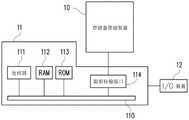
图1是根据本发明的一范例实施例所示出的主机系统、存储器存储装置及输入/输出(I/O)装置的示意图。图2是根据本发明的另一范例实施例所示出的主机系统、存储器存储装置及I/O装置的示意图。FIG. 1 is a schematic diagram of a host system, a memory storage device and an input/output (I/O) device according to an exemplary embodiment of the present invention. FIG. 2 is a schematic diagram of a host system, a memory storage device and an I/O device according to another exemplary embodiment of the present invention.
请参照图1与图2,主机系统11一般包括处理器111、随机存取存储器(randomaccess memory,RAM)112、只读存储器(read only memory,ROM)113及数据传输接口114。处理器111、随机存取存储器112、只读存储器113及数据传输接口114皆电性连接至系统总线(system bus)110。Referring to FIG. 1 and FIG. 2 , the
在本范例实施例中,主机系统11是通过数据传输接口114与存储器存储装置10电性连接。例如,主机系统11可经由数据传输接口114将数据存储至存储器存储装置10或从存储器存储装置10中读取数据。此外,主机系统11是通过系统总线110与I/O装置12电性连接。例如,主机系统11可经由系统总线110将输出信号传送至I/O装置12或从I/O装置12接收输入信号。In this exemplary embodiment, the
在本范例实施例中,处理器111、随机存取存储器112、只读存储器113及数据传输接口114可设置在主机系统11的主机板20上。数据传输接口114的数目可以是一或多个。通过数据传输接口114,主机板20可以经由有线或无线方式电性连接至存储器存储装置10。存储器存储装置10可例如是U盘201、存储卡202、固态硬盘(Solid State Drive,SSD)203或无线存储器存储装置204。无线存储器存储装置204可例如是近距离无线通讯(Near FieldCommunication,NFC)存储器存储装置、无线传真(WiFi)存储器存储装置、蓝牙(Bluetooth)存储器存储装置或低功耗蓝牙存储器存储装置(例如,iBeacon)等以各式无线通讯技术为基础的存储器存储装置。此外,主机板20也可以通过系统总线110电性连接至全球定位系统(Global Positioning System,GPS)模块205、网络接口卡206、无线传输装置207、键盘208、屏幕209、喇叭210等各式I/O装置。例如,在一范例实施例中,主机板20可通过无线传输装置207存取无线存储器存储装置204。In this exemplary embodiment, the
在一范例实施例中,所提及的主机系统为可实质地与存储器存储装置配合以存储数据的任意系统。虽然在上述范例实施例中,主机系统是以电脑系统来作说明,然而,图3是根据本发明的另一范例实施例所示出的主机系统与存储器存储装置的示意图。请参照图3,在另一范例实施例中,主机系统31也可以是数码相机、摄影机、通讯装置、音频播放器、视频播放器或平板电脑等系统,而存储器存储装置30可为其所使用的安全数字(SecureDigital,SD)卡32、小型快闪(Compact Flash,CF)卡33或嵌入式存储装置34等各式非易失性存储器存储装置。嵌入式存储装置34包括嵌入式多媒体卡(embedded Multi MediaCard,eMMC)341和/或嵌入式多芯片封装(embedded Multi Chip Package,eMCP)存储装置342等各类型将存储器模块直接电性连接于主机系统的基板上的嵌入式存储装置。In an example embodiment, reference to a host system is substantially any system that can cooperate with a memory storage device to store data. Although in the above exemplary embodiments, the host system is described as a computer system, however, FIG. 3 is a schematic diagram of a host system and a memory storage device according to another exemplary embodiment of the present invention. Please refer to FIG. 3 , in another exemplary embodiment, the
图4是根据本发明的一范例实施例所示出的存储器存储装置的概要方块图。FIG. 4 is a schematic block diagram of a memory storage device according to an exemplary embodiment of the present invention.
请参照图4,存储器存储装置10包括连接接口单元402、存储器控制电路单元404与可复写式非易失性存储器模块406。Referring to FIG. 4 , the
连接接口单元402用以将存储器存储装置10电性连接至主机系统11。在本范例实施例中,连接接口单元402是相容于串行高级技术附件(Serial Advanced TechnologyAttachment,SATA)标准。然而,必须了解的是,本发明不限于此,连接接口单元402也可以是符合并行高级技术附件(Parallel Advanced Technology Attachment,PATA)标准、电气和电子工程师协会(Institute of Electrical and Electronic Engineers,IEEE)1394标准、高速周边零件连接接口(Peripheral Component Interconnect Express,PCIExpress)标准、通用串行总线(Universal Serial Bus,USB)标准、SD接口标准、超高速一代(Ultra High Speed-I,UHS-I)接口标准、超高速二代(Ultra High Speed-II,UHS-II)接口标准、存储棒(Memory Stick,MS)接口标准、MCP接口标准、MMC接口标准、eMMC接口标准、通用快闪存储器(Universal Flash Storage,UFS)接口标准、eMCP接口标准、CF接口标准、整合式驱动电子接口(Integrated Device Electronics,IDE)标准或其他适合的标准。连接接口单元402可与存储器控制电路单元404封装在一个芯片中,或者连接接口单元402是布设于一包含存储器控制电路单元404的芯片外。The
存储器控制电路单元404用以执行以硬件型式或固件型式实作的多个逻辑门或控制指令并且根据主机系统11的指令在可复写式非易失性存储器模块406中进行数据的写入、读取与抹除等运作。The memory
可复写式非易失性存储器模块406是电性连接至存储器控制电路单元404并且用以存储主机系统11所写入的数据。可复写式非易失性存储器模块406可以是单阶存储单元(Single Level Cell,SLC)NAND型快闪存储器模块(即,一个存储单元中可存储1个比特的快闪存储器模块)、多阶存储单元(Multi Level Cell,MLC)NAND型快闪存储器模块(即,一个存储单元中可存储2个比特的快闪存储器模块)、复数阶存储单元(Triple Level Cell,TLC)NAND型快闪存储器模块(即,一个存储单元中可存储3个比特的快闪存储器模块)、其他快闪存储器模块或其他具有相同特性的存储器模块。The rewritable
可复写式非易失性存储器模块406中的每一个存储单元是以电压(以下也称为临界电压)的改变来存储一或多个比特。具体来说,每一个存储单元的控制栅极(controlgate)与通道之间有一个电荷捕捉层。通过施予一写入电压至控制栅极,可以改变电荷补捉层的电子量,进而改变存储单元的临界电压。此改变存储单元的临界电压的操作也称为“把数据写入至存储单元”或“程序化(programming)存储单元”。随着临界电压的改变,可复写式非易失性存储器模块406中的每一个存储单元具有多个存储状态。通过施予读取电压可以判断一个存储单元是属于哪一个存储状态,藉此取得此存储单元所存储的一或多个比特。Each memory cell in the rewritable
在本范例实施例中,可复写式非易失性存储器模块406的存储单元会构成多个实体程序化单元,并且此些实体程序化单元会构成多个实体抹除单元。具体来说,同一条字线上的存储单元会组成一或多个实体程序化单元。若每一个存储单元可存储2个以上的比特,则同一条字线上的实体程序化单元至少可被分类为下实体程序化单元与上实体程序化单元。例如,一存储单元的最低有效比特(Least Significant Bit,LSB)是属于下实体程序化单元,并且一存储单元的最高有效比特(Most Significant Bit,MSB)是属于上实体程序化单元。一般来说,在MLC NAND型快闪存储器中,下实体程序化单元的写入速度会大于上实体程序化单元的写入速度,和/或下实体程序化单元的可靠度是高于上实体程序化单元的可靠度。In this exemplary embodiment, the storage units of the rewritable
在本范例实施例中,实体程序化单元为程序化的最小单元。即,实体程序化单元为写入数据的最小单元。例如,实体程序化单元为实体页面(page)或是实体扇(sector)。若实体程序化单元为实体页面,则此些实体程序化单元通常包括数据比特区与冗余(redundancy)比特区。数据比特区包含多个实体扇,用以存储使用者数据,而冗余比特区用以存储系统数据(例如,错误更正码等管理数据)。在本范例实施例中,数据比特区包含32个实体扇,且一个实体扇的大小为512比特组(byte,B)。然而,在其他范例实施例中,数据比特区中也可包含8个、16个或数目更多或更少的实体扇,并且每一个实体扇的大小也可以是更大或更小。另一方面,实体抹除单元为抹除的最小单位。也即,每一实体抹除单元含有最小数目之一并被抹除的存储单元。例如,实体抹除单元为实体区块(block)。In this exemplary embodiment, the entity programming unit is the smallest unit of programming. That is, the entity programming unit is the smallest unit for writing data. For example, the entity programming unit is an entity page (page) or an entity sector (sector). If the physical programming units are physical pages, these physical programming units usually include data bit areas and redundancy (redundancy) bit areas. The data bit area includes a plurality of physical sectors for storing user data, and the redundant bit area is used for storing system data (eg, management data such as error correction codes). In this exemplary embodiment, the data bit area includes 32 physical sectors, and the size of one physical sector is 512 bits (byte, B). However, in other exemplary embodiments, the data bit area may also include 8, 16 or more or less physical sectors, and the size of each physical sector may also be larger or smaller. On the other hand, the entity erasing unit is the smallest unit of erasing. That is, each physical erase unit contains a minimum number of memory cells that are erased. For example, the physical erasing unit is a physical block.
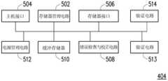
图5是根据本发明的一范例实施例所示出的存储器控制电路单元的概要方块图。FIG. 5 is a schematic block diagram of a memory control circuit unit according to an exemplary embodiment of the present invention.
请参照图5,存储器控制电路单元404包括存储器管理电路502、主机接口504及存储器接口506。Referring to FIG. 5 , the memory
存储器管理电路502用以控制存储器控制电路单元404的整体运作。具体来说,存储器管理电路502具有多个控制指令,并且在存储器存储装置10运作时,此些控制指令会被执行以进行数据的写入、读取与抹除等运作。以下说明存储器管理电路502的操作时,等同于说明存储器控制电路单元404的操作。The
在本范例实施例中,存储器管理电路502的控制指令是以固件型式来实作。例如,存储器管理电路502具有微处理器单元(未示出)与只读存储器(未示出),并且此些控制指令是被烧录至此只读存储器中。当存储器存储装置10运作时,此些控制指令会由微处理器单元来执行以进行数据的写入、读取与抹除等运作。In this exemplary embodiment, the control commands of the
在另一范例实施例中,存储器管理电路502的控制指令也可以程序码型式存储于可复写式非易失性存储器模块406的特定区域(例如,存储器模块中专用于存放系统数据的系统区)中。此外,存储器管理电路502具有微处理器单元(未示出)、只读存储器(未示出)及随机存取存储器(未示出)。特别是,此只读存储器具有开机码(boot code),并且当存储器控制电路单元404被致能时,微处理器单元会先执行此开机码来将存储于可复写式非易失性存储器模块406中的控制指令载入至存储器管理电路502的随机存取存储器中。之后,微处理器单元会运转此些控制指令以进行数据的写入、读取与抹除等运作。In another exemplary embodiment, the control instructions of the
此外,在另一范例实施例中,存储器管理电路502的控制指令也可以一硬件型式来实作。例如,存储器管理电路502包括微控制器、存储单元管理电路、存储器写入电路、存储器读取电路、存储器抹除电路与数据处理电路。存储单元管理电路、存储器写入电路、存储器读取电路、存储器抹除电路与数据处理电路是电性连接至微控制器。存储单元管理电路用以管理可复写式非易失性存储器模块406的存储单元或其群组。存储器写入电路用以对可复写式非易失性存储器模块406下达写入指令序列以将数据写入至可复写式非易失性存储器模块406中。存储器读取电路用以对可复写式非易失性存储器模块406下达读取指令序列以从可复写式非易失性存储器模块406中读取数据。存储器抹除电路用以对可复写式非易失性存储器模块406下达抹除指令序列以将数据从可复写式非易失性存储器模块406中抹除。数据处理电路用以处理欲写入至可复写式非易失性存储器模块406的数据以及从可复写式非易失性存储器模块406中读取的数据。写入指令序列、读取指令序列及抹除指令序列可各别包括一或多个程序码或指令码并且用以指示可复写式非易失性存储器模块406执行相对应的写入、读取及抹除等操作。在一范例实施例中,存储器管理电路502还可以下达其他类型的指令序列给可复写式非易失性存储器模块406以指示执行相对应的操作。In addition, in another exemplary embodiment, the control instructions of the
主机接口504是电性连接至存储器管理电路502并且用以接收与识别主机系统11所传送的指令与数据。也就是说,主机系统11所传送的指令与数据会通过主机接口504来传送至存储器管理电路502。在本范例实施例中,主机接口504是相容于SATA标准。然而,必须了解的是本发明不限于此,主机接口504也可以是相容于PATA标准、IEEE 1394标准、PCIExpress标准、USB标准、SD标准、UHS-I标准、UHS-II标准、MS标准、MMC标准、eMMC标准、UFS标准、CF标准、IDE标准或其他适合的数据传输标准。The
存储器接口506是电性连接至存储器管理电路502并且用以存取可复写式非易失性存储器模块406。也就是说,欲写入至可复写式非易失性存储器模块406的数据会经由存储器接口506转换为可复写式非易失性存储器模块406所能接受的格式。具体来说,若存储器管理电路502要存取可复写式非易失性存储器模块406,存储器接口506会传送对应的指令序列。例如,这些指令序列可包括指示写入数据的写入指令序列、指示读取数据的读取指令序列、指示抹除数据的抹除指令序列、以及用以指示各种存储器操作(例如,改变读取电压准位或执行垃圾回收操作等等)的相对应的指令序列。这些指令序列例如是由存储器管理电路502产生并且通过存储器接口506传送至可复写式非易失性存储器模块406。这些指令序列可包括一或多个信号,或是在总线上的数据。这些信号或数据可包括指令码或程序码。例如,在读取指令序列中,会包括读取的识别码、存储器地址等信息。The
在一范例实施例中,存储器控制电路单元404还包括错误检查与校正电路508、缓冲存储器510与电源管理电路512。In an exemplary embodiment, the memory
错误检查与校正电路508是电性连接至存储器管理电路502并且用以执行错误检查与校正操作以确保数据的正确性。具体来说,当存储器管理电路502从主机系统11中接收到写入指令时,错误检查与校正电路508会为对应此写入指令的数据产生对应的错误更正码(error correcting code,ECC)和/或错误检查码(error detecting code,EDC),并且存储器管理电路502会将对应此写入指令的数据与对应的错误更正码和/或错误检查码写入至可复写式非易失性存储器模块406中。之后,当存储器管理电路502从可复写式非易失性存储器模块406中读取数据时会同时读取此数据对应的错误更正码和/或错误检查码,并且错误检查与校正电路508会依据此错误更正码和/或错误检查码对所读取的数据执行错误检查与校正操作。The error checking and correcting
缓冲存储器510是电性连接至存储器管理电路502并且用以暂存来自于主机系统11的数据与指令或来自于可复写式非易失性存储器模块406的数据。电源管理电路512是电性连接至存储器管理电路502并且用以控制存储器存储装置10的电源。The
在一范例实施例中,存储器控制电路单元404还包括验证电路513与514。验证电路513与514皆电性连接至存储器管理电路502且皆支持数据的加密与解密。在本范例实施例中,验证电路513使用RSA等非对称式(asymmetric)加密算法,而验证电路514则使用进阶加密标准(Advanced Encryption Standard,AES)等对称式加密算法。然而,在另一范例实施例中,验证电路513与514皆可以支持其他类型的加密算法,只要验证电路513与514采用不同的加密算法即可。此外,在另一范例实施例中,验证电路513与514也可以设置于存储器管理电路502内部或以软件/固件的方式实施。In an exemplary embodiment, the memory
图6是根据本发明的一范例实施例所示出的管理可复写式非易失性存储器模块的示意图。FIG. 6 is a schematic diagram of managing a rewritable non-volatile memory module according to an exemplary embodiment of the present invention.
请参照图6,存储器管理电路502会将可复写式非易失性存储器模块406的实体单元610(0)~610(B)逻辑地分组至存储区601与替换区602。存储区601中的实体单元610(0)~610(A)是用以存储数据,而替换区602中的实体单元610(A+1)~610(B)则是用以替换存储区601中损坏的实体单元。例如,若从某一个实体单元中读取的数据所包含的错误过多而无法被更正时,此实体单元会被视为是损坏的实体单元。须注意的是,若替换区602中没有可用的实体抹除单元,则存储器管理电路502可能会将整个存储器存储装置10宣告为写入保护(write protect)状态,而无法再写入数据。Referring to FIG. 6 , the
在本范例实施例中,每一个实体单元是指一个实体抹除单元。然而,在另一范例实施例中,一个实体单元也可以是指一个实体地址、一个实体程序化单元或由多个连续或不连续的实体地址组成。存储器管理电路502会配置逻辑单元612(0)~612(C)以映射存储区601中的实体单元610(0)~610(A)。在本范例实施例中,每一个逻辑单元是指一个逻辑地址。然而,在另一范例实施例中,一个逻辑单元也可以是指一个逻辑程序化单元、一个逻辑抹除单元或者由多个连续或不连续的逻辑地址组成。此外,逻辑单元612(0)~612(C)中的每一者可被映射至一或多个实体单元。In this exemplary embodiment, each physical unit refers to a physical erasing unit. However, in another exemplary embodiment, a physical unit may also refer to a physical address, a physical programming unit, or consist of multiple continuous or discontinuous physical addresses. The
在本范例实施例中,存储器管理电路502会将逻辑单元与实体单元之间的映射关系(也称为逻辑-实体地址映射关系)记录于至少一逻辑-实体地址映射表。当主机系统11欲从存储器存储装置10读取数据或写入数据至存储器存储装置10时,存储器管理电路502可根据此逻辑-实体地址映射表来执行对于存储器存储装置10的数据存取操作。In this exemplary embodiment, the
在本范例实施例中,主机系统11安装有开发者工具程序,且主机系统11可通过此开发者工具程序下达开发者指令给存储器存储装置10,以指示存储器存储装置10执行特定的系统操作。须注意的是,在存储器存储装置10接收开发者指令之前,存储器存储装置10会通过至少两个交握操作来验证主机系统11,以确认主机系统11是否为开发者工具程序的合法拥有者,和/或确认主机系统11是否使用合法的开发者工具程序。In this exemplary embodiment, the
在本范例实施例中,用来验证主机系统11的交握操作包括第一交握操作与第二交握操作。第二交握操作是在主机系统11通过第一交握操作的验证后执行。在主机系统11通过第一交握操作与第二交握操作的验证后,在开发者指令传输阶段中,主机系统11可传送开发者指令给存储器存储装置10,且存储器存储装置10可传送对应于此开发者指令的数据给主机系统11。然而,在另一范例实施例中,用来验证主机系统11的交握操作还可以包括更多的交握操作,只要存储器存储装置10可经由此些交握操作来验证主机系统11即可。此外,在一范例实施例中,开发者工具程序及至少部分用于前述交握操作的数据是隐藏式地存储在主机系统11的存储媒体中,以避免被攻击者直接存取(例如复制到其他装置)。In this exemplary embodiment, the handshake operation used to verify the
图7是根据本发明的一范例实施例所示出的主机系统的存储媒体的示意图。请参照图7,在本范例实施例中,主机系统11包括存储媒体710。存储媒体710可以是可插拔地电性连接至主机系统11的外接式存储装置(例如U盘或外接式硬盘),或者是属于主机系统11内部的存储电路。存储媒体710具有隐藏存储区711与公开存储区712。隐藏存储区711存储有硬件加密模块721、身份验证模块722及开发者工具程序723。公开存储区712存储有开发者工具载入器731。FIG. 7 is a schematic diagram of a storage medium of a host system according to an exemplary embodiment of the present invention. Referring to FIG. 7 , in this exemplary embodiment, the
在本范例实施例中,隐藏存储区711与公开存储区712预设都是隐藏的。在隐藏状态下,使用者无法经由主机系统11的档案系统存取隐藏存储区711与公开存储区712。身份验证模块722存储有身份验证信息。例如,此身份验证信息包括预设账号与预设密码。在本范例实施例中,身份验证模块722可接收使用者通过主机系统11的信号输入装置输入的身份信息并基于身份验证信息对输入的身份信息进行验证。例如,身份验证模块722可比对使用者输入的账号与预设账号并比对使用者输入的密码与预设密码。若使用者输入的账号与预设账号相同且使用者输入的密码与预设密码相同,则身份验证模块722可将公开存储区712解除隐藏。反之,若使用者输入的账号与预设账号不相同和/或使用者输入的密码与预设密码不相同,则身份验证模块722将公开存储区712维持在隐藏状态。In this exemplary embodiment, both the hidden
在将公开存储区712解除隐藏后,使用者可以经由主机系统11的档案系统中对应至公开存储区712的逻辑地址存取公开存储区712。此外,在将公开存储区712解除隐藏后,开发者工具载入器731可被启动。须注意的是,无论使用者是否输入正确的身份信息,隐藏存储区711始终维持在隐藏状态而无法被使用者存取。然而,在另一范例实施例中,存储媒体710也可以不采用隐藏机制、不预设将公开存储区712隐藏、或采用其他的验证机制来将公开存储区712解除隐藏,本发明不加以限制。以下将以图5与图7搭配图8至图11对本发明的主机系统验证方法进行说明。After the
图8是根据本发明的一范例实施例所示出的主机系统验证方法的准备阶段的操作时序示意图。请参照图7与图8,主机系统验证方法的准备阶段包括步骤S801至S803。在步骤S801中,硬件加密模块721可根据一基本信息动态的产生金钥信息PbKey(也称为第一金钥信息)与PvKey(也称为第二金钥信息)。在一范例实施例中,此基本信息可为身份验证模块722所存储的身份验证信息。然而,在另一范例实施例中,此基本信息也可以是动态产生的随机数或其他数据,本发明不加以限制。FIG. 8 is a schematic diagram of the operation sequence of the preparation phase of the verification method for the host system according to an exemplary embodiment of the present invention. Please refer to FIG. 7 and FIG. 8 , the preparation stage of the host system verification method includes steps S801 to S803 . In step S801, the
在本范例实施例中,硬件加密模块721是基于基本信息使用公开金钥加密(public-key cryptography)算法产生金钥信息PbKey与PvKey,故金钥信息PbKey与PvKey属于非对称式金钥对。例如,金钥信息PbKey为此非对称式金钥对的公钥,而金钥信息PvKey为此非对称式金钥对的私钥。然而,在另一范例实施例中,硬件加密模块721也可以是使用其他类型的加密算法来产生金钥信息PbKey与PvKey或使用对称式金钥加密算法产生一金钥信息来供验证使用,本发明不加以限制。In this exemplary embodiment, the
在步骤S802中,主机系统11会将所产生的金钥信息PbKey提供给存储器存储装置10。金钥信息PvKey则存储于隐藏存储区711中。在步骤S803中,存储器存储装置10会存储金钥信息PbKey。例如,金钥信息PbKey可被存储于图4的可复写式非易失性存储器模块406。至此,完成主机系统验证方法的准备阶段。尔后,一旦开发者工具载入器731被启动,则可进入主机系统验证方法的第一交握操作。In step S802 , the
图9是根据本发明的一范例实施例所示出的主机系统验证方法的第一交握操作的操作时序示意图。请参照图5、图7及图9,主机系统验证方法的第一交握操作可包括步骤S901~S909。在步骤S901中,主机系统11的开发者工具载入器731启动隐藏存储区711中的开发者工具程序723。在步骤S902中,主机系统11(例如被启动的开发者工具程序723)可发送通知信息给存储器存储装置10,以通知存储器存储装置10开始执行第一交握操作。FIG. 9 is a schematic diagram of the operation sequence of the first handshake operation of the host system verification method according to an exemplary embodiment of the present invention. Please refer to FIG. 5 , FIG. 7 and FIG. 9 , the first handshake operation of the host system verification method may include steps S901 - S909 . In step S901 , the
在步骤S903中,存储器存储装置10动态产生验证信息Cert(也称为第一验证信息)。例如,验证信息Cert可为存储器管理电路502产生的一次性验证信息。在步骤S904中,存储器存储装置10基于金钥信息PbKey与验证信息Cert产生加密信息CI1(也称为第一加密信息)。例如,验证电路513可基于金钥信息PbKey使用RSA加密算法来加密验证信息Cert以产生加密信息CI1。在步骤S905中,存储器存储装置10将加密信息CI1传送给主机系统11。In step S903, the
在步骤S906中,主机系统11接收加密信息CI1并基于金钥信息PvKey与加密信息CI1产生加密信息CI2(也称为第二加密信息)。例如,开发者工具程序723可基于金钥信息PvKey使用RSA加密算法来解密加密信息CI1以获得验证信息Cert。然后,开发者工具程序723可基于金钥信息PvKey使用RSA加密算法来加密所获得的验证信息Cert以产生加密信息CI2。在步骤S907中,主机系统11将加密信息CI2传送给存储器存储装置10。In step S906, the
在步骤S908中,存储器存储装置10基于金钥信息PbKey与加密信息CI2产生比对信息Cert’(也称为第一比对信息)。例如,验证电路513可基于金钥信息PbKey使用RSA加密算法来解密加密信息CI2以产生比对信息Cert’。然后,存储器存储装置10会根据验证信息Cert与比对信息Cert’来验证主机系统11。例如,在步骤S909中,存储器管理电路502会比对验证信息Cert与比对信息Cert’。若验证信息Cert与比对信息Cert’相同,表示主机系统11所使用的金钥信息PvKey与存储器存储装置10所使用的金钥信息PbKey是相互匹配的,故存储器管理电路502可判定主机系统11通过第一交握操作的验证。反之,若验证信息Cert与比对信息Cert’不相同,表示主机系统11所使用的金钥信息PvKey与存储器存储装置10所使用的金钥信息PbKey不是相互匹配的,故存储器管理电路502可判定主机系统11未通过第一交握操作的验证。若主机系统11通过第一交握操作的验证,则存储器管理电路502允许进入主机系统验证方法的第二交握操作。反之,若主机系统11未通过第一交握操作的验证,则存储器管理电路502不允许进入主机系统验证方法的第二交握操作。换言之,在第一交握操作中,存储器管理电路502是利用加密信息CI2来验证主机系统11是否可执行第二交握操作。In step S908, the
图10是根据本发明的一范例实施例所示出的主机系统验证方法的第二交握操作的操作时序示意图。请参照图5、图7及图10,主机系统验证方法的第二交握操作可包括步骤S1001~S1011。在步骤S1001中,主机系统11通知存储器存储装置10执行第二交握操作。例如,开发者工具程序723可向存储器存储装置10传送一个验证请求。FIG. 10 is a schematic diagram of the operation sequence of the second handshake operation of the host system verification method according to an exemplary embodiment of the present invention. Referring to FIG. 5 , FIG. 7 and FIG. 10 , the second handshake operation of the host system verification method may include steps S1001 - S1011 . In step S1001, the
在接收到此验证请求后,在步骤S1002中,存储器存储装置10动态产生验证信息RN(也称为第二验证信息)。例如,验证信息RN可为存储器管理电路502产生的一次性验证信息。在步骤S1003中,存储器存储装置10基于金钥信息PbKey与验证信息RN产生加密信息CI3(也称为第三加密信息)。例如,验证电路513可基于金钥信息PbKey使用RSA加密算法来加密验证信息RN以产生加密信息CI3。在步骤S1004中,存储器存储装置10将加密信息CI3传送给主机系统11。After receiving the verification request, in step S1002, the
在步骤S1005中,主机系统11接收加密信息CI3并基于金钥信息PvKey与加密信息CI3获得验证信息RN。例如,开发者工具程序723可基于金钥信息PvKey使用RSA加密算法来解密加密信息CI3以获得验证信息RN。在步骤S1006中,主机系统11基于验证信息RN产生验证信息SKey(也称为第三验证信息)。例如,开发者工具程序723可基于验证信息RN与一个金钥参数动态产生一次性的验证信息SKey。In step S1005, the
另一范例实施例,在产生验证信息RN后,在步骤S1007中,存储器存储装置10会基于验证信息RN产生验证信息SKey。例如,存储器管理电路502可基于验证信息RN与一个金钥参数动态产生一次性的验证信息SKey。须注意的是,在本范例实施例中,主机系统11与存储器存储装置10是使用相同的验证信息RN以及相同的金钥参数来产生验证信息SKey,故所产生的验证信息SKey也会相同。此验证信息SKey可用于在后续的开发者指令传输阶段中加密在主机系统11与存储器存储装置10之间传输的数据。In another exemplary embodiment, after the verification information RN is generated, in step S1007 , the
在步骤S1008中,主机系统11基于验证信息RN与验证信息SKey产生加密信息CI4(也称为第四加密信息)。例如,开发者工具程序723可基于验证信息SKey使用AES加密算法来加密验证信息RN以产生加密信息CI4。在步骤S1009中,主机系统11将加密信息CI4传送给存储器存储装置10。In step S1008, the
在接收到加密信息CI4后,在步骤S1010中,存储器存储装置10基于验证信息SKey与加密信息CI4产生比对信息RN’(也称为第二比对信息)。例如,验证电路514可基于验证信息SKey使用AES加密算法来解密加密信息CI4以产生比对信息RN’。然后,存储器存储装置10会根据验证信息RN与比对信息RN’来验证主机系统11。例如,在步骤S1011中,存储器管理电路502会比对验证信息RN与比对信息RN’。若验证信息RN与比对信息RN’相同,表示主机系统11所使用的金钥信息PvKey与存储器存储装置10所使用的金钥信息PbKey是相互匹配的,且主机系统11与存储器存储装置10是使用相同的验证信息SKey,故存储器管理电路502可判定主机系统11通过第二交握操作的验证。反之,若验证信息RN与比对信息RN’不相同,表示主机系统11所使用的金钥信息PvKey与存储器存储装置10所使用的金钥信息PbKey不是相互匹配的,和/或主机系统11与存储器存储装置10不是使用相同的验证信息SKey,故存储器管理电路502可判定主机系统11未通过第二交握操作的验证。若主机系统11通过第二交握操作的验证,则存储器管理电路502允许进入主机系统验证方法的开发者指令传输阶段。反之,若主机系统11未通过第二交握操作的验证,则存储器管理电路502不允许进入主机系统验证方法的开发者指令传输阶段。换言之,在第二交握操作中,存储器管理电路502是利用加密信息CI4来验证主机系统11是否可执行(或进入)开发者指令传输阶段。After receiving the encrypted information CI4, in step S1010, the
图11是根据本发明的一范例实施例所示出的主机系统验证方法的开发者指令传输阶段的操作时序示意图。请参照图5、图7及图11,主机系统验证方法的开发者指令传输阶段可包括步骤S1101~S1103。在步骤S1101中,主机系统11根据验证信息SKey加密开发者指令。例如,开发者工具程序723可动态产生一或多个开发者指令,且所产生的开发者指令可用以指示存储器存储装置10执行特定系统操作。开发者工具程序723可基于验证信息SKey使用AES加密算法来加密开发者指令。在步骤S1102中,主机系统11将已加密的开发者指令传送给存储器存储装置10。FIG. 11 is a schematic diagram of the operation sequence of the developer instruction transmission stage of the host system verification method according to an exemplary embodiment of the present invention. Please refer to FIG. 5 , FIG. 7 and FIG. 11 , the developer instruction transmission stage of the host system verification method may include steps S1101 - S1103 . In step S1101, the
在步骤S1103中,存储器存储装置10接收已加密的开发者指令并根据验证信息SKey解析已加密的开发者指令。例如,验证电路514可基于验证信息SKey使用AES加密算法来解密已加密的开发者指令。根据已解密的开发者指令,存储器管理电路502可执行系统参数更新、固件更新或回传特定信息给主机系统11等系统操作。此外,在图11的另一范例实施例中,存储器存储装置10的验证电路514也可使用验证信息SKey加密欲传送至主机系统11的数据,且主机系统11的开发者工具程序723也可以使用相同的验证信息SKey来解密来自存储器存储装置10的数据,在此便不赘述。In step S1103, the
从另一角度来看,在如图9的第一交握操作中,存储器存储装置10是根据验证信息Cert来验证主机系统11的合法性;而在如图10的第二交握操作中,存储器存储装置10是根据验证信息RN来验证主机系统11的合法性。此外,在如图11的开发者指令传输阶段中,存储器存储装置10是根据验证信息SKey来解析从主机系统11接收的开发者指令。特别是,验证信息Cert、验证信息RN及验证信息SKey各不相同。例如,验证信息Cert、验证信息RN及验证信息SKey分别为在相应操作/阶段中产生的一次性随机数。From another point of view, in the first handshake operation as shown in FIG. 9 , the
须注意的是,虽然在前述范例实施例中主要是以RSA加密算法搭配AES加密算法作为加/解密的范例进行说明,然而,在另一范例实施例中,第一交握操作、第二交握操作及开发者指令传输阶段中所采用的加密算法可使用相同或不同的各种算法,皆可根据实务需求加以调整,本发明不加以限制。在一范例实施例中,加密信息CI3(即第三加密信息)使用的加密算法(例如RSA)对数据的保护强度高于加密信息CI4(即第四加密信息)使用的加密算法(例如AES)对数据的保护强度,但本发明不限于此。在一范例实施例中,不同加密信息所使用的加密算法及数据保护强度皆可以视实务上的需求加以调整。It should be noted that although in the foregoing exemplary embodiments, the RSA encryption algorithm and the AES encryption algorithm are mainly used as an example of encryption/decryption for illustration, however, in another exemplary embodiment, the first handshake operation, the second handshake operation, and the second handshake operation The encryption algorithms used in the gripping operation and the developer instruction transmission stage can use the same or different algorithms, and can be adjusted according to practical needs, which is not limited by the present invention. In an exemplary embodiment, the encryption algorithm (such as RSA) used by the encrypted information CI3 (ie, the third encrypted information) has higher protection strength for data than the encryption algorithm (such as AES) used by the encrypted information CI4 (ie, the fourth encrypted information) Strength of protection for data, but the invention is not limited thereto. In an exemplary embodiment, the encryption algorithms and data protection strengths used for different encrypted information can be adjusted according to practical requirements.
在一范例实施例中,主机系统11于开发者指令传输阶段中使用以与存储器存储装置10沟通的指令集不同于主机系统11于通用指令传输阶段中使用以与存储器存储装置10沟通的指令集。例如,在开发者指令传输阶段中,主机系统11是使用特定的指令集(也称为开发者指令集)来下达指示系统参数更新、固件更新或回传特定信息等系统操作的开发者指令给主机系统11;而在通用指令传输阶段中,主机系统11是使用通用指令集来下达数据读取、写入及抹除等通用数据存取指令以指示存储器存储装置10执行相应的数据存取操作。在一范例实施例中,通用指令传输阶段不须经由第一交握操作和/或第二交握操作的验证即可进入。例如,在一范例实施例中,当建立主机系统11与存储器存储装置10之间的连线后,通用指令传输阶段可自动启用,且主机系统11可在此通用指令传输阶段中传输通用数据存取指令。In an exemplary embodiment, the command set used by the
图12是根据本发明的一范例实施例所示出的存储器存储系统的示意图。请参照图12,在本范例实施例中,外接式存储装置1200相同或相似于图7的存储媒体710。在将外接式存储装置1200电连接至主机系统1211后,主机系统1211可经由外接式存储装置1200与存储器存储装置1210执行前述范例实施例所提及的第一交握操作。若主机系统1211通过第一交握操作的验证,则主机系统1211可进一步经由外接式存储装置1200与存储器存储装置1210执行前述范例实施例所提及的第二交握操作。若主机系统1211也通过第二交握操作的验证,则主机系统1211可更进一步经由外接式存储装置1200在开发者指令传输阶段中与存储器存储装置1210进行加密通讯以传输开发者指令。FIG. 12 is a schematic diagram of a memory storage system according to an exemplary embodiment of the present invention. Please refer to FIG. 12 , in this exemplary embodiment, an
图13是根据本发明的另一范例实施例所示出的存储器存储系统的示意图。请参照图13,在本范例实施例中,外接式存储装置1300相同或相似于图7的存储媒体710。在将外接式存储装置1300电连接至主机系统1301后,主机系统1301可将外接式存储装置1300所存储的开发者工具程序下载至主机系统1311(1)~1311(N)。同时,主机系统1301可将外接式存储装置1300中至少部分用于前述第一交握操作与第二交握操作的信息(例如,金钥信息PvKey等)提供至主机系统1311(1)~1311(N)。来自主机系统1301(或外接式存储装置1300)的信息可以暂存于主机系统1311(1)~1311(N)的缓冲存储器中。藉此,主机系统1311(1)~1311(N)可根据各自的缓冲存储器中的开发者工具程序来分别与存储器存储装置1310(1)~1310(N)执行如图9至图11的操作,在此便不赘述。例如,图13的范例实施例可以是描述存储器存储装置1310(1)~1310(N)在生产端生产或维修的场景。FIG. 13 is a schematic diagram of a memory storage system according to another exemplary embodiment of the present invention. Referring to FIG. 13 , in this exemplary embodiment, an
综上所述,存储器存储装置可通过不同的验证信息在至少两个交握操作中验证主机系统,且在交握操作中传输的信息皆经过加密。此外,存储器存储装置与主机系统可通过所述交握操作交换在开发者指令传输阶段中用于加密和/或解析开发者指令的验证信息,从而增强存储器存储装置对主机系统的验证能力,并降低攻击者成功使用未经授权的开发者程序来修改存储器存储装置的参数或偷取存储器存储装置中的数据的机率。To sum up, the memory storage device can authenticate the host system in at least two handshake operations through different authentication information, and the information transmitted in the handshake operations is all encrypted. In addition, the memory storage device and the host system can exchange verification information for encrypting and/or analyzing the developer command during the developer command transmission phase through the handshake operation, thereby enhancing the verification capability of the memory storage device to the host system, and The chances of an attacker successfully using an unauthorized developer program to modify parameters of a memory storage device or steal data in the memory storage device are reduced.
虽然本发明已以实施例揭示如上,然其并非用以限定本发明,任何所属技术领域中技术人员,在不脱离本发明的精神和范围内,当可作些许的更改与润饰,故本发明的保护范围当视权利要求所界定者为准。Although the present invention has been disclosed above with the embodiments, it is not intended to limit the present invention. Any person skilled in the art can make some changes and modifications without departing from the spirit and scope of the present invention. Therefore, the present invention The scope of protection shall prevail as defined by the claims.
Claims (32)
Priority Applications (1)
| Application Number | Priority Date | Filing Date | Title |
|---|---|---|---|
| CN201810062088.8ACN110069934B (en) | 2018-01-23 | 2018-01-23 | Memory storage system, host system verification method and memory storage device |
Applications Claiming Priority (1)
| Application Number | Priority Date | Filing Date | Title |
|---|---|---|---|
| CN201810062088.8ACN110069934B (en) | 2018-01-23 | 2018-01-23 | Memory storage system, host system verification method and memory storage device |
Publications (2)
| Publication Number | Publication Date |
|---|---|
| CN110069934A CN110069934A (en) | 2019-07-30 |
| CN110069934Btrue CN110069934B (en) | 2022-12-13 |
Family
ID=67364826
Family Applications (1)
| Application Number | Title | Priority Date | Filing Date |
|---|---|---|---|
| CN201810062088.8AActiveCN110069934B (en) | 2018-01-23 | 2018-01-23 | Memory storage system, host system verification method and memory storage device |
Country Status (1)
| Country | Link |
|---|---|
| CN (1) | CN110069934B (en) |
Families Citing this family (1)
| Publication number | Priority date | Publication date | Assignee | Title |
|---|---|---|---|---|
| CN113378216A (en)* | 2021-05-29 | 2021-09-10 | 深圳市得一微电子有限责任公司 | eMMC control method, system and storage medium thereof |
Citations (6)
| Publication number | Priority date | Publication date | Assignee | Title |
|---|---|---|---|---|
| TW200627325A (en)* | 2005-01-19 | 2006-08-01 | Lightuning Tech Inc | Storage device and method for protecting data stored therein |
| TW201333701A (en)* | 2012-02-10 | 2013-08-16 | Phison Electronics Corp | Data protecting method, memory controller and memory storage device |
| CN103257938A (en)* | 2012-02-21 | 2013-08-21 | 群联电子股份有限公司 | Data protection method, memory controller and memory storage device |
| CN103427984A (en)* | 2012-05-24 | 2013-12-04 | 三星电子株式会社 | Apparatus for generating secure key using device ID and user authentication information |
| CN104346103A (en)* | 2013-08-09 | 2015-02-11 | 群联电子股份有限公司 | Instruction execution method, memory controller and memory storage device |
| CN104573537A (en)* | 2013-10-11 | 2015-04-29 | 群联电子股份有限公司 | Data processing method, memory storage device and memory control circuit unit |
Family Cites Families (6)
| Publication number | Priority date | Publication date | Assignee | Title |
|---|---|---|---|---|
| US9092635B2 (en)* | 2006-03-31 | 2015-07-28 | Gemalto Sa | Method and system of providing security services using a secure device |
| DE102007000589B9 (en)* | 2007-10-29 | 2010-01-28 | Bundesdruckerei Gmbh | Method for protecting a chip card against unauthorized use, chip card and chip card terminal |
| US8806572B2 (en)* | 2009-05-30 | 2014-08-12 | Cisco Technology, Inc. | Authentication via monitoring |
| GB201119747D0 (en)* | 2011-11-15 | 2011-12-28 | Fxi Technologies As | Portable storage devices for electronic devices |
| TWI447580B (en)* | 2012-04-03 | 2014-08-01 | Phison Electronics Corp | Memory space managing method, and memory controller and memory storage device using the same |
| US10127055B2 (en)* | 2015-10-16 | 2018-11-13 | Quanta Computer Inc. | iSCSI based bare metal OS image deployment and diskless boot |
- 2018
- 2018-01-23CNCN201810062088.8Apatent/CN110069934B/enactiveActive
Patent Citations (6)
| Publication number | Priority date | Publication date | Assignee | Title |
|---|---|---|---|---|
| TW200627325A (en)* | 2005-01-19 | 2006-08-01 | Lightuning Tech Inc | Storage device and method for protecting data stored therein |
| TW201333701A (en)* | 2012-02-10 | 2013-08-16 | Phison Electronics Corp | Data protecting method, memory controller and memory storage device |
| CN103257938A (en)* | 2012-02-21 | 2013-08-21 | 群联电子股份有限公司 | Data protection method, memory controller and memory storage device |
| CN103427984A (en)* | 2012-05-24 | 2013-12-04 | 三星电子株式会社 | Apparatus for generating secure key using device ID and user authentication information |
| CN104346103A (en)* | 2013-08-09 | 2015-02-11 | 群联电子股份有限公司 | Instruction execution method, memory controller and memory storage device |
| CN104573537A (en)* | 2013-10-11 | 2015-04-29 | 群联电子股份有限公司 | Data processing method, memory storage device and memory control circuit unit |
Also Published As
| Publication number | Publication date |
|---|---|
| CN110069934A (en) | 2019-07-30 |
Similar Documents
| Publication | Publication Date | Title |
|---|---|---|
| TWI641966B (en) | Memory storage system, host system authentication method and memory storage device | |
| CN106462509B (en) | Apparatus and method for securing access protection schemes | |
| US11736276B2 (en) | Delegation of cryptographic key to a memory sub-system | |
| US20210243035A1 (en) | Multi-factor authentication enabled memory sub-system | |
| US11928192B2 (en) | Vendor unique command authentication system, and a host device, storage device, and method employing the same | |
| TWI688965B (en) | Data writing method, memory control circuit unit and memory storage device | |
| US20220158823A1 (en) | Validating data stored in memory using cryptographic hashes | |
| US20130080787A1 (en) | Memory storage apparatus, memory controller and password verification method | |
| CN113841129A (en) | Data proof in memory | |
| TW201329707A (en) | Data protecting method, memory controller and memory storage apparatus | |
| TW202137004A (en) | Data transfer method and memory storage device | |
| CN110069934B (en) | Memory storage system, host system verification method and memory storage device | |
| CN115599407B (en) | Firmware burning method, firmware burning system and memory storage device | |
| TWI829250B (en) | Signature verification method, memory storage device and memory control circuit unit | |
| CN102375943B (en) | Identification code generation method, memory management method, controller and storage system | |
| CN105868643A (en) | Data protection method, memory control circuit unit and memory storage device | |
| CN113448488B (en) | Data transfer method and memory storage device | |
| CN112416240B (en) | Data writing method, memory control circuit unit and memory storage device | |
| CN115238321A (en) | Signature verification method, memory storage device, and memory control circuit unit | |
| CN106155564A (en) | Storage device management method and system and storage device thereof | |
| CN106033321A (en) | Response reading method and data transmission system | |
| CN105988935A (en) | Smart card management method, memory storage device and memory control circuit unit |
Legal Events
| Date | Code | Title | Description |
|---|---|---|---|
| PB01 | Publication | ||
| PB01 | Publication | ||
| SE01 | Entry into force of request for substantive examination | ||
| SE01 | Entry into force of request for substantive examination | ||
| GR01 | Patent grant | ||
| GR01 | Patent grant |