CN109962084B - Organic light emitting diode display substrate, display device and manufacturing method - Google Patents
Organic light emitting diode display substrate, display device and manufacturing methodDownload PDFInfo
- Publication number
- CN109962084B CN109962084BCN201711338884.1ACN201711338884ACN109962084BCN 109962084 BCN109962084 BCN 109962084BCN 201711338884 ACN201711338884 ACN 201711338884ACN 109962084 BCN109962084 BCN 109962084B
- Authority
- CN
- China
- Prior art keywords
- shielding layer
- sub
- filter unit
- thin film
- film transistor
- Prior art date
- Legal status (The legal status is an assumption and is not a legal conclusion. Google has not performed a legal analysis and makes no representation as to the accuracy of the status listed.)
- Active
Links
Images

Classifications
- H—ELECTRICITY
- H10—SEMICONDUCTOR DEVICES; ELECTRIC SOLID-STATE DEVICES NOT OTHERWISE PROVIDED FOR
- H10K—ORGANIC ELECTRIC SOLID-STATE DEVICES
- H10K59/00—Integrated devices, or assemblies of multiple devices, comprising at least one organic light-emitting element covered by group H10K50/00
- H10K59/30—Devices specially adapted for multicolour light emission
- H10K59/35—Devices specially adapted for multicolour light emission comprising red-green-blue [RGB] subpixels
- H—ELECTRICITY
- H10—SEMICONDUCTOR DEVICES; ELECTRIC SOLID-STATE DEVICES NOT OTHERWISE PROVIDED FOR
- H10K—ORGANIC ELECTRIC SOLID-STATE DEVICES
- H10K59/00—Integrated devices, or assemblies of multiple devices, comprising at least one organic light-emitting element covered by group H10K50/00
- H10K59/30—Devices specially adapted for multicolour light emission
- H10K59/38—Devices specially adapted for multicolour light emission comprising colour filters or colour changing media [CCM]
- H—ELECTRICITY
- H10—SEMICONDUCTOR DEVICES; ELECTRIC SOLID-STATE DEVICES NOT OTHERWISE PROVIDED FOR
- H10K—ORGANIC ELECTRIC SOLID-STATE DEVICES
- H10K59/00—Integrated devices, or assemblies of multiple devices, comprising at least one organic light-emitting element covered by group H10K50/00
- H10K59/30—Devices specially adapted for multicolour light emission
- H10K59/35—Devices specially adapted for multicolour light emission comprising red-green-blue [RGB] subpixels
- H10K59/351—Devices specially adapted for multicolour light emission comprising red-green-blue [RGB] subpixels comprising more than three subpixels, e.g. red-green-blue-white [RGBW]
- H—ELECTRICITY
- H10—SEMICONDUCTOR DEVICES; ELECTRIC SOLID-STATE DEVICES NOT OTHERWISE PROVIDED FOR
- H10K—ORGANIC ELECTRIC SOLID-STATE DEVICES
- H10K50/00—Organic light-emitting devices
- H10K50/80—Constructional details
- H10K50/85—Arrangements for extracting light from the devices
- H—ELECTRICITY
- H10—SEMICONDUCTOR DEVICES; ELECTRIC SOLID-STATE DEVICES NOT OTHERWISE PROVIDED FOR
- H10K—ORGANIC ELECTRIC SOLID-STATE DEVICES
- H10K50/00—Organic light-emitting devices
- H10K50/80—Constructional details
- H10K50/86—Arrangements for improving contrast, e.g. preventing reflection of ambient light
- H—ELECTRICITY
- H10—SEMICONDUCTOR DEVICES; ELECTRIC SOLID-STATE DEVICES NOT OTHERWISE PROVIDED FOR
- H10K—ORGANIC ELECTRIC SOLID-STATE DEVICES
- H10K59/00—Integrated devices, or assemblies of multiple devices, comprising at least one organic light-emitting element covered by group H10K50/00
- H10K59/10—OLED displays
- H10K59/12—Active-matrix OLED [AMOLED] displays
- H10K59/121—Active-matrix OLED [AMOLED] displays characterised by the geometry or disposition of pixel elements
- H10K59/1213—Active-matrix OLED [AMOLED] displays characterised by the geometry or disposition of pixel elements the pixel elements being TFTs
- H—ELECTRICITY
- H10—SEMICONDUCTOR DEVICES; ELECTRIC SOLID-STATE DEVICES NOT OTHERWISE PROVIDED FOR
- H10K—ORGANIC ELECTRIC SOLID-STATE DEVICES
- H10K59/00—Integrated devices, or assemblies of multiple devices, comprising at least one organic light-emitting element covered by group H10K50/00
- H10K59/10—OLED displays
- H10K59/12—Active-matrix OLED [AMOLED] displays
- H10K59/126—Shielding, e.g. light-blocking means over the TFTs
- H—ELECTRICITY
- H10—SEMICONDUCTOR DEVICES; ELECTRIC SOLID-STATE DEVICES NOT OTHERWISE PROVIDED FOR
- H10D—INORGANIC ELECTRIC SEMICONDUCTOR DEVICES
- H10D86/00—Integrated devices formed in or on insulating or conducting substrates, e.g. formed in silicon-on-insulator [SOI] substrates or on stainless steel or glass substrates
- H10D86/40—Integrated devices formed in or on insulating or conducting substrates, e.g. formed in silicon-on-insulator [SOI] substrates or on stainless steel or glass substrates characterised by multiple TFTs
- H10D86/441—Interconnections, e.g. scanning lines
- H—ELECTRICITY
- H10—SEMICONDUCTOR DEVICES; ELECTRIC SOLID-STATE DEVICES NOT OTHERWISE PROVIDED FOR
- H10D—INORGANIC ELECTRIC SEMICONDUCTOR DEVICES
- H10D86/00—Integrated devices formed in or on insulating or conducting substrates, e.g. formed in silicon-on-insulator [SOI] substrates or on stainless steel or glass substrates
- H10D86/40—Integrated devices formed in or on insulating or conducting substrates, e.g. formed in silicon-on-insulator [SOI] substrates or on stainless steel or glass substrates characterised by multiple TFTs
- H10D86/60—Integrated devices formed in or on insulating or conducting substrates, e.g. formed in silicon-on-insulator [SOI] substrates or on stainless steel or glass substrates characterised by multiple TFTs wherein the TFTs are in active matrices
- H—ELECTRICITY
- H10—SEMICONDUCTOR DEVICES; ELECTRIC SOLID-STATE DEVICES NOT OTHERWISE PROVIDED FOR
- H10K—ORGANIC ELECTRIC SOLID-STATE DEVICES
- H10K2102/00—Constructional details relating to the organic devices covered by this subclass
- H10K2102/10—Transparent electrodes, e.g. using graphene
- H10K2102/101—Transparent electrodes, e.g. using graphene comprising transparent conductive oxides [TCO]
- H10K2102/103—Transparent electrodes, e.g. using graphene comprising transparent conductive oxides [TCO] comprising indium oxides, e.g. ITO
Landscapes
- Engineering & Computer Science (AREA)
- Microelectronics & Electronic Packaging (AREA)
- Physics & Mathematics (AREA)
- Geometry (AREA)
- Optics & Photonics (AREA)
- Electroluminescent Light Sources (AREA)
- Devices For Indicating Variable Information By Combining Individual Elements (AREA)
Abstract
Description
Translated fromChinese技术领域technical field
本发明涉及显示技术领域,尤其涉及一种有机发光二极管显示基板、显示装置及制作方法。The present invention relates to the field of display technology, and in particular, to an organic light emitting diode display substrate, a display device and a manufacturing method.
背景技术Background technique
现有的底发射型有机发光二极管(OLED)显示基板主要包括:衬底基板以及设置在所述衬底基板上的多个像素单元,每一所述像素单元包括多种颜色的亚像素单元,每一所述亚像素单元包括薄膜晶体管(TFT)驱动层和底发射型有机发光二极管,薄膜晶体管驱动层又包括开关薄膜晶体管和驱动薄膜晶体管。现有的底发射型有机发光二极管显示基板中,开关薄膜晶体管和底发射型有机发光二极管之间没有遮挡,底发射型有机发光二极管发射的光线能够照射至开关薄膜晶体管上,当开关薄膜晶体管为氧化物(Oxide)薄膜晶体管时,该种类型的开关薄膜晶体管对于蓝光等低波段光比较敏感,当有蓝光等低波段光照射到开关薄膜晶体管上时,容易造成负向漂移,当负向漂移超出开关薄膜晶体管的关闭电压(Vgl)时,会引起开关薄膜晶体管开启,导致对应的电容漏电,进一步导致显示异常。The existing bottom emission organic light emitting diode (OLED) display substrate mainly includes: a base substrate and a plurality of pixel units arranged on the base substrate, each of the pixel units includes sub-pixel units of multiple colors, Each of the sub-pixel units includes a thin film transistor (TFT) driving layer and a bottom emission type organic light emitting diode, and the thin film transistor driving layer further includes a switching thin film transistor and a driving thin film transistor. In the existing bottom emission type organic light emitting diode display substrate, there is no shield between the switching thin film transistor and the bottom emission type organic light emitting diode, and the light emitted by the bottom emission type organic light emitting diode can be irradiated on the switching thin film transistor. When the switching thin film transistor is Oxide thin film transistor, this type of switching thin film transistor is more sensitive to low-band light such as blue light. When low-band light such as blue light is irradiated on the switching thin film transistor, it is easy to cause negative drift. When the negative drift When the off voltage (Vgl) of the switching thin film transistor is exceeded, the switching thin film transistor will be turned on, resulting in leakage of the corresponding capacitor, which further leads to abnormal display.
发明内容SUMMARY OF THE INVENTION
有鉴于此,本发明提供一种有机发光二极管显示基板、显示装置及制作方法,用于解决现有的底发射型有机发光二极管显示基板上的开关薄膜晶体管因被光照射异常开启而导致的显示异常的问题。In view of this, the present invention provides an organic light emitting diode display substrate, a display device and a manufacturing method, which are used to solve the display problem caused by abnormal opening of the switching thin film transistor on the existing bottom emission type organic light emitting diode display substrate due to light irradiation. unusual question.
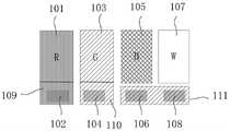
为解决上述技术问题,本发明提供一种有机发光二极管显示基板,包括衬底基板以及设置在所述衬底基板上的多个像素单元,每一所述像素单元包括多个的亚像素单元,每一所述亚像素单元包括开关薄膜晶体管和底发射型有机发光二极管,所述有机发光二极管显示基板还包括:遮光层,所述遮光层位于所述有机发光二极管与所述开关薄膜晶体管之间,所述遮光层在所述衬底基板上的正投影完全覆盖所述开关薄膜晶体管的半导体区域在所述衬底基板上的正投影。In order to solve the above technical problems, the present invention provides an organic light emitting diode display substrate, comprising a base substrate and a plurality of pixel units arranged on the base substrate, each of the pixel units includes a plurality of sub-pixel units, Each of the sub-pixel units includes a switching thin film transistor and a bottom emission organic light emitting diode, and the organic light emitting diode display substrate further includes: a light shielding layer, the light shielding layer is located between the organic light emitting diode and the switching thin film transistor , the orthographic projection of the light shielding layer on the base substrate completely covers the orthographic projection of the semiconductor region of the switching thin film transistor on the base substrate.
优选地,所述有机发光二极管显示基板为白光有机发光二极管显示基板,所述有机发光二极管为白光有机发光二极管,每一所述亚像素单元还包括:与所述亚像素单元的颜色对应的滤光单元。Preferably, the organic light emitting diode display substrate is a white light organic light emitting diode display substrate, the organic light emitting diode is a white light organic light emitting diode, and each of the sub-pixel units further includes: a filter corresponding to the color of the sub-pixel unit. light unit.
优选地,每一所述像素单元所在区域内设置有第一颜色的第一滤光单元和第二颜色的第二滤光单元,所述第一滤光单元能够过滤掉蓝光,所述第二滤光单元能够透射蓝光,所述遮光层与所述第一滤光单元同层同材料设置。Preferably, a first filter unit of a first color and a second filter unit of a second color are arranged in the area where each pixel unit is located, the first filter unit can filter out blue light, and the second filter unit is capable of filtering out blue light. The filter unit can transmit blue light, and the light shielding layer and the first filter unit are provided with the same layer and material.
优选地,所述第一颜色包括红色和/或绿色,所述第二颜色包括蓝色和/或白色。Preferably, the first color includes red and/or green, and the second color includes blue and/or white.
优选地,每一所述像素单元中,所有亚像素单元的开关薄膜晶体管均位于所述滤光单元所在区域的同一侧,并靠近所述第一滤光单元设置,所述遮光层与所述第一滤光单元相连。Preferably, in each of the pixel units, the switching thin film transistors of all sub-pixel units are located on the same side of the area where the filter unit is located, and are arranged close to the first filter unit, and the light shielding layer and the The first filter unit is connected.
优选地,每一所述像素单元包括红色亚像素单元、绿色亚像素单元、蓝色亚像素单元和白色亚像素单元,每一所述像素单元所在区域内设置有遮光层、红色亚像素单元对应的红色滤光单元、红色亚像素单元对应的开关薄膜晶体管、绿色亚像素单元对应的绿色滤光单元、绿色亚像素单元对应的开关薄膜晶体管、蓝色亚像素单元对应的蓝色滤光单元、蓝色亚像素单元对应的开关薄膜晶体管、白色亚像素单元对应的白色滤光单元、白色亚像素单元对应的开关薄膜晶体管,所述红色滤光单元、绿色滤光单元、蓝色滤光单元和白色滤光单元呈两行两列排列,所述红色滤光单元和绿色滤光单元位于同一行,所述蓝色滤光单元和白色滤光单元位于同一行,所述遮光层包括红色遮光层和绿色遮光层,所述红色遮光层与所述红色滤光单元相连,所述绿色遮光层与所述绿色滤光单元相连,所述红色遮光层和绿色遮光层在衬底基板上的正投影完全覆盖所述像素单元中的所有开关薄膜晶体管的半导体区域在衬底基板上的正投影。Preferably, each of the pixel units includes a red sub-pixel unit, a green sub-pixel unit, a blue sub-pixel unit and a white sub-pixel unit, and a light shielding layer is provided in the area where each of the pixel units is located, and the red sub-pixel unit corresponds to The red filter unit, the switching thin film transistor corresponding to the red sub-pixel unit, the green filter unit corresponding to the green sub-pixel unit, the switching thin-film transistor corresponding to the green sub-pixel unit, the blue filter unit corresponding to the blue sub-pixel unit, The switching thin film transistor corresponding to the blue sub-pixel unit, the white filter unit corresponding to the white sub-pixel unit, and the switching thin film transistor corresponding to the white sub-pixel unit, the red filter unit, the green filter unit, the blue filter unit and the The white filter units are arranged in two rows and two columns, the red filter unit and the green filter unit are located in the same row, the blue filter unit and the white filter unit are located in the same row, and the light shielding layer includes a red light shielding layer and green light-shielding layer, the red light-shielding layer is connected with the red filter unit, the green light-shielding layer is connected with the green filter unit, the orthographic projection of the red light-shielding layer and the green light-shielding layer on the base substrate The orthographic projection of the semiconductor region on the base substrate that completely covers all switching thin film transistors in the pixel unit.
优选地,所述红色亚像素单元的开关薄膜晶体管的半导体区域在衬底基板上的正投影位于红色遮光层在衬底基板上的正投影内,所述绿色亚像素单元的开关薄膜晶体管的半导体区域在衬底基板上的正投影位于绿色遮光层在衬底基板上的正投影内,所述蓝色亚像素单元和白色亚像素单元两者中的一者的开关薄膜晶体管的半导体区域在衬底基板上的正投影位于所述红色遮光层在衬底基板上的正投影内,另一者的开关薄膜晶体管的半导体区域在衬底基板上的正投影位于绿色遮光层在衬底基板上的正投影内。Preferably, the orthographic projection of the semiconductor region of the switching thin film transistor of the red sub-pixel unit on the base substrate is located within the orthographic projection of the red light shielding layer on the base substrate, and the semiconductor region of the switching thin film transistor of the green sub-pixel unit The orthographic projection of the region on the base substrate is located within the orthographic projection of the green light-shielding layer on the base substrate, and the semiconductor region of the switching thin film transistor of one of the blue sub-pixel unit and the white sub-pixel unit is on the substrate. The orthographic projection on the base substrate is located within the orthographic projection of the red light-shielding layer on the base substrate, and the orthographic projection of the semiconductor region of the other switching thin film transistor on the base substrate is located within the orthographic projection of the green light-shielding layer on the base substrate. in the orthographic projection.
优选地,每一所述像素单元中,所有亚像素单元的开关薄膜晶体管均位于所述滤光单元所在区域的同一侧,并分别靠近所述对应的滤光单元设置,所述遮光层包括第一遮光层和第二遮光层,所述第一遮光层与所述第一滤光单元相连,所述第一遮光层在所述衬底基板上的正投影完全覆盖所述第一颜色的亚像素单元的开关薄膜晶体管的半导体区域在所述衬底基板上的正投影,所述第二遮光层与所述第二滤光单元不相连,所述第二遮光层在所述衬底基板上的正投影完全覆盖所述第二颜色的亚像素单元的开关薄膜晶体管的半导体区域在所述衬底基板上的正投影。Preferably, in each of the pixel units, the switching thin film transistors of all sub-pixel units are located on the same side of the region where the filter unit is located, and are respectively disposed close to the corresponding filter unit, and the light shielding layer includes a first a light-shielding layer and a second light-shielding layer, the first light-shielding layer is connected to the first filter unit, and the orthographic projection of the first light-shielding layer on the base substrate completely covers the sub-surface of the first color The orthographic projection of the semiconductor region of the switching thin film transistor of the pixel unit on the base substrate, the second light shielding layer is not connected to the second filter unit, and the second light shielding layer is on the base substrate The orthographic projection completely covers the orthographic projection of the semiconductor region of the switching thin film transistor of the second color sub-pixel unit on the base substrate.
优选地,每一所述像素单元包括红色亚像素单元、绿色亚像素单元、蓝色亚像素单元和白色亚像素单元,每一所述像素单元所在区域内设置有遮光层、红色亚像素单元对应的红色滤光单元、红色亚像素单元对应的开关薄膜晶体管、绿色亚像素单元对应的绿色滤光单元、绿色亚像素单元对应的开关薄膜晶体管、蓝色亚像素单元对应的蓝色滤光单元、蓝色亚像素单元对应的开关薄膜晶体管、白色亚像素单元对应的白色滤光单元和白色亚像素单元对应的开关薄膜晶体管,所述红色滤光单元、绿色滤光单元、蓝色滤光单元和白色滤光单元呈一行四列排列,所述第一遮光层包括红色遮光层和绿色遮光层,所述红色遮光层与所述红色滤光单元相连,所述红色遮光层在所述衬底基板上的正投影完全覆盖所述红色亚像素单元的开关薄膜晶体管的半导体区域在所述衬底基板上的正投影,所述绿色遮光层与所述绿色滤光单元相连,所述绿色遮光层在所述衬底基板上的正投影完全覆盖所述绿色亚像素单元的开关薄膜晶体管的半导体区域在所述衬底基板上的正投影,所述第二遮光层为红色遮光层或绿色遮光层,所述第二遮光层在所述衬底基板上的正投影完全覆盖所述蓝色亚像素单元以及白色亚像素单元的开关薄膜晶体管的半导体区域在所述衬底基板上的正投影,所述第二遮光层与所述蓝色滤光单元以及白色滤光单元间隔设置不相连。Preferably, each of the pixel units includes a red sub-pixel unit, a green sub-pixel unit, a blue sub-pixel unit and a white sub-pixel unit, and a light shielding layer is provided in the area where each of the pixel units is located, and the red sub-pixel unit corresponds to The red filter unit, the switching thin film transistor corresponding to the red sub-pixel unit, the green filter unit corresponding to the green sub-pixel unit, the switching thin-film transistor corresponding to the green sub-pixel unit, the blue filter unit corresponding to the blue sub-pixel unit, The switching thin film transistor corresponding to the blue sub-pixel unit, the white filter unit corresponding to the white sub-pixel unit, and the switching thin film transistor corresponding to the white sub-pixel unit, the red filter unit, the green filter unit, the blue filter unit and the The white filter units are arranged in one row and four columns, the first light-shielding layer includes a red light-shielding layer and a green light-shielding layer, the red light-shielding layer is connected to the red filter unit, and the red light-shielding layer is on the base substrate The orthographic projection on the red sub-pixel unit completely covers the orthographic projection of the semiconductor region of the switching thin film transistor of the red sub-pixel unit on the base substrate, the green light-shielding layer is connected to the green filter unit, and the green light-shielding layer is in The orthographic projection on the base substrate completely covers the orthographic projection of the semiconductor region of the switching thin film transistor of the green sub-pixel unit on the base substrate, and the second light shielding layer is a red light shielding layer or a green light shielding layer, The orthographic projection of the second light-shielding layer on the base substrate completely covers the orthographic projection of the semiconductor regions of the switching thin film transistors of the blue sub-pixel unit and the white sub-pixel unit on the base substrate, and the The second light shielding layer is not connected to the blue filter unit and the white filter unit at intervals.
优选地,所述开关薄膜晶体管为氧化物薄膜晶体管。Preferably, the switching thin film transistor is an oxide thin film transistor.
本发明还提供一种有机发光二极管显示装置,包括上述有机发光二极管显示基板。The present invention also provides an organic light emitting diode display device, comprising the above organic light emitting diode display substrate.
本发明还提供一种有机发光二极管显示基板的制作方法,用于制作上述有机发光二极管显示基板,包括:The present invention also provides a method for manufacturing an organic light-emitting diode display substrate, which is used for manufacturing the above-mentioned organic light-emitting diode display substrate, including:
提供一衬底基板;providing a base substrate;
在所述衬底基板上形成多个像素单元和遮光层,每一所述像素单元包括多种颜色的亚像素单元,每一所述亚像素单元包括开关薄膜晶体管和底发射型有机发光二极管,所述遮光层位于所述有机发光二极管与所述开关薄膜晶体管之间,所述遮光层在所述衬底基板上的正投影完全覆盖所述开关薄膜晶体管的半导体区域在所述衬底基板上的正投影。A plurality of pixel units and a light shielding layer are formed on the base substrate, each of the pixel units includes sub-pixel units of multiple colors, and each of the sub-pixel units includes a switching thin film transistor and a bottom emission organic light emitting diode, The light shielding layer is located between the organic light emitting diode and the switching thin film transistor, and the orthographic projection of the light shielding layer on the base substrate completely covers the semiconductor region of the switching thin film transistor on the base substrate orthographic projection.
本发明的上述技术方案的有益效果如下:The beneficial effects of the above-mentioned technical solutions of the present invention are as follows:
在底发射型有机发光二极管和开关薄膜晶体管之间设置遮光层,该遮光层至少将所述开关薄膜晶体管的半导体区域(即沟道区域)遮挡住,使其不被有机发光二极管发射的光照射到,从而可以改善开关薄膜晶体管的半导体区域被光照射导致的负飘问题,提高了显示效果。A light-shielding layer is arranged between the bottom-emission organic light-emitting diode and the switching thin-film transistor, and the light-shielding layer at least shields the semiconductor region (ie, the channel region) of the switching thin-film transistor from being irradiated by the light emitted by the organic light-emitting diode Thus, the problem of negative drift caused by the light irradiation of the semiconductor region of the switching thin film transistor can be improved, and the display effect can be improved.
附图说明Description of drawings
为了更清楚地说明本发明实施例的技术方案,下面将对本发明实施例的描述中所需要使用的附图作简单地介绍,显而易见地,下面描述中的附图仅仅是本发明的一些实施例,对于本领域普通技术人员来讲,在不付出创造性劳动性的前提下,还可以根据这些附图获得其他的附图。In order to illustrate the technical solutions of the embodiments of the present invention more clearly, the following briefly introduces the drawings that are used in the description of the embodiments of the present invention. Obviously, the drawings in the following description are only some embodiments of the present invention. , for those of ordinary skill in the art, other drawings can also be obtained from these drawings without creative labor.
图1为本发明实施例一的白光有机发光二极管显示基板的结构示意图;FIG. 1 is a schematic structural diagram of a white light organic light emitting diode display substrate according to Embodiment 1 of the present invention;
图2为本发明实施例二的白光有机发光二极管显示基板的结构示意图。FIG. 2 is a schematic structural diagram of a white light organic light emitting diode display substrate according to Embodiment 2 of the present invention.
具体实施方式Detailed ways
为使本发明实施例的目的、技术方案和优点更加清楚,下面将结合本发明实施例的附图,对本发明实施例的技术方案进行清楚、完整地描述。显然,所描述的实施例是本发明的一部分实施例,而不是全部的实施例。基于所描述的本发明的实施例,本领域普通技术人员所获得的所有其他实施例,都属于本发明保护的范围。In order to make the purpose, technical solutions and advantages of the embodiments of the present invention clearer, the technical solutions of the embodiments of the present invention will be clearly and completely described below with reference to the accompanying drawings of the embodiments of the present invention. Obviously, the described embodiments are some, but not all, embodiments of the present invention. Based on the described embodiments of the present invention, all other embodiments obtained by those of ordinary skill in the art fall within the protection scope of the present invention.
本发明实施例提供一种有机发光二极管显示基板,包括衬底基板以及设置在所述衬底基板上的多个像素单元,每一所述像素单元包括多个的亚像素单元,每一所述亚像素单元包括开关薄膜晶体管和底发射型有机发光二极管,所述有机发光二极管显示基板还包括:遮光层,所述遮光层位于所述有机发光二极管和所述开关薄膜晶体管之间,所述遮光层在所述衬底基板上的正投影完全覆盖所述开关薄膜晶体管的半导体区域在所述衬底基板上的正投影。An embodiment of the present invention provides an organic light emitting diode display substrate, including a base substrate and a plurality of pixel units disposed on the base substrate, each of the pixel units includes a plurality of sub-pixel units, each of the pixel units The sub-pixel unit includes a switching thin film transistor and a bottom emission organic light emitting diode, and the organic light emitting diode display substrate further includes: a light shielding layer, the light shielding layer is located between the organic light emitting diode and the switching thin film transistor, and the light shielding layer is located between the organic light emitting diode and the switching thin film transistor. The orthographic projection of the layer on the base substrate completely covers the orthographic projection of the semiconductor region of the switching thin film transistor on the base substrate.
本发明实施例中,在底发射型有机发光二极管和开关薄膜晶体管之间设置遮光层,该遮光层至少将所述开关薄膜晶体管的半导体区域(即沟道区域)遮挡住,使其不被有机发光二极管发射的光照射到,从而可以改善开关薄膜晶体管的半导体区域被光照射导致的负飘问题,提高了显示效果。In the embodiment of the present invention, a light-shielding layer is provided between the bottom-emission organic light-emitting diode and the switching thin film transistor, and the light shielding layer at least shields the semiconductor region (ie, the channel region) of the switching thin film transistor, so that it is not blocked by the organic light-emitting diode. The light emitted by the light emitting diode is irradiated, so that the negative drift problem caused by the light irradiation of the semiconductor region of the switching thin film transistor can be improved, and the display effect is improved.
由于光存在折射和散射,因而如果只有开关薄膜晶体管的半导体区域被遮光层覆盖,难以保证半导体区域不被光照射到,因而优选地,本发明实施例中,所述遮光层在所述衬底基板上的正投影完全覆盖所述开关薄膜晶体管在所述衬底基板上的正投影,即,所述开关薄膜晶体管整个完全被所述遮光层遮挡住,从而进一步保证开关薄膜晶体管不被光照射到。Due to refraction and scattering of light, if only the semiconductor region of the switching thin film transistor is covered by a light shielding layer, it is difficult to ensure that the semiconductor region is not irradiated by light. The orthographic projection on the substrate completely covers the orthographic projection of the switching thin film transistor on the base substrate, that is, the switching thin film transistor is completely blocked by the light shielding layer, thereby further ensuring that the switching thin film transistor is not illuminated by light arrive.
本发明实施例中,遮挡层的具体尺寸可以根据具体的结构以及遮光层的厚度等做出调整。In the embodiment of the present invention, the specific size of the shielding layer can be adjusted according to the specific structure and the thickness of the shielding layer.
本发明实施例中的开关薄膜晶体管可以是氧化物薄膜晶体管,由于在底发射型有机发光二极管和开关薄膜晶体管之间设置遮光层,该遮光层至少将所述开关薄膜晶体管的半导体区域(即沟道区域)遮挡住,使其不被有机发光二极管发射的蓝光等低波段光照射到,从而可以避免开关薄膜晶体管的半导体区域被蓝光等低波段光照射导致开关薄膜晶体管异常开启的问题,提高了显示效果。当然,本发明实施例中的开关薄膜晶体管也可以为其他类型的薄膜晶体管。The switching thin film transistor in the embodiment of the present invention may be an oxide thin film transistor. Since a light shielding layer is provided between the bottom emission organic light emitting diode and the switching thin film transistor, the light shielding layer at least shields the semiconductor region of the switching thin film transistor (that is, the channel channel area), so that it is not irradiated by low-band light such as blue light emitted by organic light-emitting diodes, so as to avoid the problem that the semiconductor region of the switching thin-film transistor is irradiated by low-band light such as blue light, causing the switching thin-film transistor to turn on abnormally, which improves the display effect. Of course, the switching thin film transistors in the embodiments of the present invention may also be other types of thin film transistors.
在本发明的一些实施例中,所述有机发光二极管显示基板为白光有机发光二极管显示基板,即,所述亚像素中的有机发光二极管为白光有机发光二极管;此时,每一所述亚像素单元还包括:与所述亚像素单元的颜色对应的滤光单元。由于白光有机发光二极管发射白光,发射的白光中包含蓝光等低波段光,因而,在白光有机发光二极管和开关薄膜晶体管之间设置遮光层,该遮光层至少将所述开关薄膜晶体管的半导体区域(即沟道区域)遮挡住,使其不被白光有机发光二极管发射的蓝光等低波段光照射到,从而可以避免开关薄膜晶体管的半导体区域被蓝光等低波段光照射导致开关薄膜晶体管异常开启的问题,提高了显示效果。In some embodiments of the present invention, the organic light emitting diode display substrate is a white light organic light emitting diode display substrate, that is, the organic light emitting diodes in the sub-pixels are white light organic light emitting diodes; in this case, each of the sub-pixels The unit further includes: a filter unit corresponding to the color of the sub-pixel unit. Since the white light organic light emitting diode emits white light, and the emitted white light includes low-band light such as blue light, a light shielding layer is arranged between the white light organic light emitting diode and the switching thin film transistor, and the light shielding layer at least shields the semiconductor region of the switching thin film transistor ( That is, the channel region) is blocked so that it is not irradiated by low-band light such as blue light emitted by white light organic light-emitting diodes, so as to avoid the problem that the semiconductor region of the switching thin film transistor is illuminated by low-band light such as blue light, causing the switching thin film transistor to be abnormally turned on. , which improves the display effect.
本发明实施例中,遮光层可以采用多种类型的遮光材料制成,本发明并不做限制。In the embodiment of the present invention, the light-shielding layer may be made of various types of light-shielding materials, which is not limited in the present invention.
在本发明的一些优选实施例中,每一所述像素单元所在区域内设置有第一颜色的第一滤光单元和第二颜色的第二滤光单元,所述第一滤光单元能够过滤掉蓝光,所述第二滤光单元能够透射蓝光,所述遮光层与所述第一滤光单元同层同材料设置。由于遮光层与第一滤光单元同层同材料设置,可以减少制作过程中采用的掩膜数量,降低了生产成本。In some preferred embodiments of the present invention, a first filter unit of a first color and a second filter unit of a second color are provided in the area where each pixel unit is located, and the first filter unit can filter When the blue light is dropped, the second filter unit can transmit blue light, and the light shielding layer and the first filter unit are provided in the same layer and the same material. Since the light-shielding layer and the first filter unit are provided in the same layer and the same material, the number of masks used in the manufacturing process can be reduced, and the production cost can be reduced.
在本发明的一些实施例中,所述第一滤光单元可以包括红色滤光单元,或者,包括绿色滤光单元,或者,同时包括红色滤光单元和绿色滤光单元。In some embodiments of the present invention, the first filter unit may include a red filter unit, or a green filter unit, or both a red filter unit and a green filter unit.
在本发明的一些实施例中,所述第二滤光单元可以包括蓝光滤光单元,例如白光有机发光二极管的像素单元的结构为红(R)、绿(G)、蓝(B)结构,即一个像素单元包括红色滤光单元、绿色滤光单元和蓝色滤光单元。所述第二滤光单元也可以同时包括蓝色滤光单元和白色滤光单元,例如白光有机发光二极管的像素单元的结构为红(R)、绿(G)、蓝(B)、白(W)结构,即一个像素单元包括红色滤光单元、绿色滤光单元、蓝色滤光单元和白色滤光单元。In some embodiments of the present invention, the second filter unit may include a blue light filter unit, for example, the structure of the pixel unit of a white light organic light emitting diode is a red (R), green (G), and blue (B) structure, That is, one pixel unit includes a red filter unit, a green filter unit and a blue filter unit. The second filter unit may also include a blue filter unit and a white filter unit. For example, the structure of the pixel unit of a white organic light emitting diode is red (R), green (G), blue (B), white ( W) structure, that is, a pixel unit includes a red filter unit, a green filter unit, a blue filter unit and a white filter unit.
本发明的一些实施例中,每一所述像素单元中,所有亚像素单元的开关薄膜晶体管均位于所述滤光单元所在区域的同一侧,并分别靠近所述对应的滤光单元设置,所述遮光层包括第一遮光层和第二遮光层,所述第一遮光层与所述第一滤光单元相连,所述第一遮光层在所述衬底基板上的正投影完全覆盖所述第一颜色的亚像素单元的开关薄膜晶体管的半导体区域在所述衬底基板上的正投影,所述第二遮光层与所述第二滤光单元不相连,所述第二遮光层在所述衬底基板上的正投影完全覆盖所述第二颜色的亚像素单元的开关薄膜晶体管的半导体区域在所述衬底基板上的正投影。In some embodiments of the present invention, in each pixel unit, the switching thin film transistors of all sub-pixel units are located on the same side of the area where the filter unit is located, and are respectively disposed close to the corresponding filter unit, so The light-shielding layer includes a first light-shielding layer and a second light-shielding layer, the first light-shielding layer is connected to the first filter unit, and the orthographic projection of the first light-shielding layer on the base substrate completely covers the The orthographic projection of the semiconductor region of the switching thin film transistor of the sub-pixel unit of the first color on the base substrate, the second light shielding layer is not connected to the second filter unit, and the second light shielding layer is in the The orthographic projection on the base substrate completely covers the orthographic projection of the semiconductor region of the switching thin film transistor of the sub-pixel unit of the second color on the base substrate.
请参考图1,在本发明的另外一些实施例中,每一所述像素单元包括红色亚像素单元、绿色亚像素单元、蓝色亚像素单元和白色亚像素单元,每一所述像素单元所在区域内设置有红色亚像素单元对应的红色滤光单元101、红色亚像素单元对应的开关薄膜晶体管102、绿色亚像素单元对应的绿色滤光单元103、绿色亚像素单元对应的开关薄膜晶体管104、蓝色亚像素单元对应的蓝色滤光单元105、蓝色亚像素单元对应的开关薄膜晶体管106、白色亚像素单元对应的白色滤光单元107、白色亚像素单元对应的开关薄膜晶体管108和遮光层,所述红色滤光单元101、绿色滤光单元103、蓝色滤光单元105和白色滤光单元107呈一行四列排列,所述遮光层包括红色遮光层109、第一绿色遮光层110和第二绿色遮光层111,所述红色遮光层109与所述红色滤光单元101相连,所述红色遮光层109在所述衬底基板上的正投影完全覆盖所述红色亚像素单元的开关薄膜晶体管102的半导体区域在所述衬底基板上的正投影,所述第一绿色遮光层110与所述绿色滤光单元103相连,所述第一绿色遮光层110在所述衬底基板上的正投影完全覆盖所述绿色亚像素单元的开关薄膜晶体管104的半导体区域在所述衬底基板上的正投影,所述第二绿色遮光层111在所述衬底基板上的正投影完全覆盖所述蓝色亚像素单元以及白色亚像素单元的开关薄膜晶体管106和108的半导体区域在所述衬底基板上的正投影,所述第二绿色遮光层111与所述蓝色滤光单元以及白色滤光单元间隔设置,不相连。Please refer to FIG. 1 , in other embodiments of the present invention, each of the pixel units includes a red sub-pixel unit, a green sub-pixel unit, a blue sub-pixel unit and a white sub-pixel unit, and each of the pixel units is located The
本发明实施例中,第二遮光层采用第二绿色遮光层111实现,在本发明的其他一些实施例中,第二遮光层也可以采用红色遮光层实现。In the embodiment of the present invention, the second light-shielding layer is implemented by the second green light-
本发明实施例中,第二绿色遮光层111不与第一绿色遮光层110相连,在本发明的其他一些实施例中,第二绿色遮光层111还可以与第一绿色遮光层110相连。In the embodiment of the present invention, the second green
上述实施例中,由于第二绿色遮光层111与蓝色滤光单元和白色滤光单元相邻,出于工艺原因,第二绿色遮光层111与蓝色滤光单元和白色滤光单元之间必须有一定的边缘间隔,因而会影响蓝色滤光单元和白色滤光单元对应的亚像素的开口率。In the above embodiment, since the second green
为解决上述问题,本发明实施例中,优选地,所有亚像素单元的开关薄膜晶体管均位于所述滤光单元所在区域的同一侧,并靠近所述第一滤光单元设置,所述遮光层与所述第一滤光单元相连。由于,第一滤光单元所在区域与开关薄膜晶体管所在区域相邻,因而遮光层可以与第一遮光单元相连,能够尽可能多的覆盖开关薄膜晶体管的更多周边区域,且不会影响亚像素的开口率。In order to solve the above problem, in the embodiment of the present invention, preferably, the switching thin film transistors of all sub-pixel units are located on the same side of the area where the filter unit is located, and are arranged close to the first filter unit, and the light shielding layer connected with the first filter unit. Since the area where the first filter unit is located is adjacent to the area where the switching thin film transistor is located, the light shielding layer can be connected to the first light shielding unit, which can cover more surrounding areas of the switching thin film transistor as much as possible without affecting the sub-pixels opening rate.
请参考图2,在本发明的一些实施例中,红色亚像素单元、绿色亚像素单元、蓝色亚像素单元和白色亚像素单元,每一所述像素单元所在区域内设置有红色亚像素单元对应的红色滤光单元101、红色亚像素单元对应的开关薄膜晶体管102、绿色亚像素单元对应的绿色滤光单元103、绿色亚像素单元对应的开关薄膜晶体管104、蓝色亚像素单元对应的蓝色滤光单元105、蓝色亚像素单元对应的开关薄膜晶体管106、白色亚像素单元对应的白色滤光单元107、白色亚像素单元对应的开关薄膜晶体管108和遮光层,所述红色滤光单元101、绿色滤光单元103、蓝色滤光单元105和白色滤光单元107呈两行两列排列,所述红色滤光单元101和绿色滤光单元103位于同一行,所述蓝色滤光单元105和白色滤光单元107位于同一行,所述遮光层包括红色遮光层109和绿色遮光层110,所述红色遮光层109与所述红色滤光单元101相连,所述绿色遮光层110与所述绿色滤光单元103相连,所述红色遮光层109和绿色遮光层110在所述衬底基板上的正投影完全覆盖对应像素单元中的所有开关薄膜晶体管(102、104、106和108)的半导体区域在衬底基板上的正投影。Please refer to FIG. 2 , in some embodiments of the present invention, a red sub-pixel unit, a green sub-pixel unit, a blue sub-pixel unit and a white sub-pixel unit are provided, and a red sub-pixel unit is arranged in the area where each of the pixel units is located The corresponding
本发明实施例中,像素单元所在区域内的所有开关薄膜晶体管均位于滤光单元的相同的一侧(即图1中的下侧),且靠近红色滤光单元101和绿色滤光单元103设置,因而,可以分别加宽红色滤光单元101和绿色滤光单元103的尺寸,形成红色遮光层109和绿色遮光层110,用于遮挡开关薄膜晶体管,使其不被白光有机发光二极管发射的蓝光等低波段光照射到,从而可以避免开关薄膜晶体管的半导体区域被蓝光等低波段光照射导致开关薄膜晶体管异常开启的问题,提高了显示效果。另外,红色遮光层109与红色滤光单元101相连,绿色遮光层110与绿色滤光单元103相连,也不会由于引入遮光层而造成亚像素开口率下降的问题。In the embodiment of the present invention, all the switching thin film transistors in the area where the pixel unit is located are located on the same side of the filter unit (ie, the lower side in FIG. 1 ), and are disposed close to the
图2所示的实施例中,所述红色亚像素单元的开关薄膜晶体管102的半导体区域在衬底基板上的正投影位于红色遮光层109在衬底基板上的正投影内,所述绿色亚像素单元的开关薄膜晶体管104的半导体区域在衬底基板上的正投影位于绿色遮光层110在衬底基板上的正投影内,所述蓝色亚像素单元的开关薄膜晶体管106的半导体区域在衬底基板上的正投影位于所述红色遮光层109在衬底基板上的正投影内,白色亚像素单元的开关薄膜晶体管108的半导体区域在衬底基板上的正投影位于绿色遮光层110在衬底基板上的正投影内。从而使得开关薄膜晶体管与对应的亚像素距离最近,避免因两者距离较远造成的工艺复杂及信号延迟的问题。In the embodiment shown in FIG. 2 , the orthographic projection of the semiconductor region of the switching
当然,在本发明的其他一些实施例中,红色亚像素单元和绿色亚像素单元的位置可以互换,蓝色亚像素单元和白色亚像素单元的位置也可以互换。Of course, in some other embodiments of the present invention, the positions of the red sub-pixel unit and the green sub-pixel unit may be interchanged, and the positions of the blue sub-pixel unit and the white sub-pixel unit may also be interchanged.
上述实施例中,白色亚像素单元的白色滤光单元107可以是一透明膜层,或者不设置任何滤光膜层。In the above-mentioned embodiment, the
通过实验验证,增加了遮光层的白光有机发光二极管显示基板的开关薄膜晶体管的负飘最大为3.5V,没有超过开关薄膜晶体管的Vgl(5.5V),因而不会出现开关薄膜晶体管异常开启,提高了显示效果。Through experimental verification, the maximum negative drift of the switching thin film transistor of the white light organic light emitting diode display substrate with the added light shielding layer is 3.5V, which does not exceed the Vgl (5.5V) of the switching thin film transistor, so there will be no abnormal opening of the switching thin film transistor. display effect.
本发明实施例还提供一种有机发光二极管显示装置,包括上述有机发光二极管显示基板。Embodiments of the present invention further provide an organic light emitting diode display device, including the above organic light emitting diode display substrate.
本发明实施例还提供一种有机发光二极管显示基板的制作方法,用于制作上述任一实施例中的有机发光二极管显示基板,所述制作方法包括:An embodiment of the present invention further provides a method for fabricating an organic light emitting diode display substrate, which is used to fabricate the organic light emitting diode display substrate in any of the above embodiments, and the fabrication method includes:
步骤11:提供一衬底基板;Step 11: providing a base substrate;
步骤12:在所述衬底基板上形成多个像素单元和遮光层,每一所述像素单元包括多种颜色的亚像素单元,每一所述亚像素单元包括开关薄膜晶体管和有机发光二极管,所述遮光层位于所述有机发光二极管与所述开关薄膜晶体管之间,所述遮光层在所述衬底基板上的正投影完全覆盖所述开关薄膜晶体管的半导体区域在所述衬底基板上的正投影。Step 12: forming a plurality of pixel units and a light shielding layer on the base substrate, each of the pixel units includes sub-pixel units of multiple colors, and each of the sub-pixel units includes a switching thin film transistor and an organic light emitting diode, The light shielding layer is located between the organic light emitting diode and the switching thin film transistor, and the orthographic projection of the light shielding layer on the base substrate completely covers the semiconductor region of the switching thin film transistor on the base substrate orthographic projection.
下面介绍一白光有机发光二极管显示基板的具体的制作过程。The specific manufacturing process of a white light organic light emitting diode display substrate is described below.
本发明实施例的白光有机发光二极管的制作方法包括以下步骤:The manufacturing method of the white light organic light emitting diode according to the embodiment of the present invention includes the following steps:
步骤21:提供一衬底基板,并进行清洗;Step 21: providing a base substrate and cleaning;
步骤22:在所述衬底基板上制作栅金属层的图形。Step 22: forming a pattern of the gate metal layer on the base substrate.
本发明实施例中,可以采用溅射(sputter)或蒸镀法沉积栅金属层,并进行图形化,形成栅金属层的图形,栅金属层的厚度可以约为220nm,材料选用Al或Cu等金属材料制作。In the embodiment of the present invention, the gate metal layer can be deposited by sputtering or evaporation, and patterned to form a pattern of the gate metal layer. The thickness of the gate metal layer can be about 220 nm, and the material is selected from Al or Cu. Made of metal material.
步骤23:采用化学沉积法(CVD)形成栅极绝缘层;Step 23: forming a gate insulating layer by chemical deposition (CVD);
步骤24:形成有源层的图形;Step 24: forming a pattern of the active layer;
本发明实施例中,可以采用sputter法沉积厚度为10~80nm的IGZO,并进行图形化,形成有源层的图形。In the embodiment of the present invention, the sputter method may be used to deposit IGZO with a thickness of 10-80 nm, and then pattern it to form the pattern of the active layer.
步骤25:形成刻蚀阻挡层的图形;Step 25: forming the pattern of the etching barrier layer;
本发明实施例中,可以采用PECVD((Plasma Enhanced Chemical VaporDeposition,等离子体增强化学的气相沉积法)沉积厚度为40~120nm的SiOx或AlOx作为刻蚀阻挡层,并进行根据图形化,形成刻蚀阻挡层的图形。In the embodiment of the present invention, PECVD ((Plasma Enhanced Chemical VaporDeposition, plasma enhanced chemical vapor deposition method) can be used to deposit SiOx or AlOx with a thickness of 40 to 120 nm as an etching barrier layer, and perform patterning to form etching Graphics of the barrier layer.
步骤26:形成源漏金属层的图形;Step 26: forming a pattern of the source-drain metal layer;
本发明实施例中,可以采用sputter法形成源漏金属层,并进行图形化形成源漏金属层的图形,源漏金属层的厚度可以约为220nm,材料采用Mo、MoW、Cu或AlNd等。In the embodiment of the present invention, the source-drain metal layer can be formed by the sputter method, and the pattern of the source-drain metal layer can be formed by patterning.
步骤27:形成钝化层的图形;Step 27: forming the pattern of the passivation layer;
本发明实施例中,可以采用PECVD法沉积厚度为200~400nm的SiOx或SiNx作为钝化层,并进行图形化,形成钝化层的图形。In the embodiment of the present invention, SiOx or SiNx with a thickness of 200-400 nm may be deposited as a passivation layer by PECVD method, and patterned to form a pattern of the passivation layer.
步骤28:分别制作R、G、B、W滤光单元,并同时形成遮光层;Step 28: making R, G, B, W filter units respectively, and forming a light shielding layer at the same time;
步骤29:形成像素电极(即白光有机发光二极管的阳极)的图形;Step 29: forming a pattern of the pixel electrode (ie the anode of the white light organic light emitting diode);
本发明实施例中,可以利用sputter法沉积厚度为40nm或135nm的ITO或者是40~135nm的IZO,并进行图形化,形成像素电极的图形。In the embodiment of the present invention, ITO with a thickness of 40 nm or 135 nm or IZO with a thickness of 40 to 135 nm can be deposited by the sputter method, and patterned to form the pattern of the pixel electrode.
步骤210:形成白光有机发光二极管的有机发光层和阴极。Step 210 : forming an organic light-emitting layer and a cathode of a white light organic light-emitting diode.
除非另作定义,本发明中使用的技术术语或者科学术语应当为本发明所属领域内具有一般技能的人士所理解的通常意义。本发明中使用的“第一”、“第二”以及类似的词语并不表示任何顺序、数量或者重要性,而只是用来区分不同的组成部分。同样,“一个”或者“一”等类似词语也不表示数量限制,而是表示存在至少一个。“连接”或者“相连”等类似的词语并非限定于物理的或者机械的连接,而是可以包括电性的连接,不管是直接的还是间接的。“上”、“下”、“左”、“右”等仅用于表示相对位置关系,当被描述对象的绝对位置改变后,则该相对位置关系也相应地改变。Unless otherwise defined, technical or scientific terms used in the present invention should have the ordinary meaning as understood by those of ordinary skill in the art to which the present invention belongs. The terms "first," "second," and similar terms used herein do not denote any order, quantity, or importance, but are merely used to distinguish different components. Likewise, "a" or "an" and the like do not denote a quantitative limitation, but rather denote the presence of at least one. Words like "connected" or "connected" are not limited to physical or mechanical connections, but may include electrical connections, whether direct or indirect. "Up", "Down", "Left", "Right", etc. are only used to represent the relative positional relationship, and when the absolute position of the described object changes, the relative positional relationship also changes accordingly.
以上所述是本发明的优选实施方式,应当指出,对于本技术领域的普通技术人员来说,在不脱离本发明所述原理的前提下,还可以作出若干改进和润饰,这些改进和润饰也应视为本发明的保护范围。The above are the preferred embodiments of the present invention. It should be pointed out that for those skilled in the art, without departing from the principles of the present invention, several improvements and modifications can be made. It should be regarded as the protection scope of the present invention.
Claims (10)
Translated fromChinesePriority Applications (6)
| Application Number | Priority Date | Filing Date | Title |
|---|---|---|---|
| CN201711338884.1ACN109962084B (en) | 2017-12-14 | 2017-12-14 | Organic light emitting diode display substrate, display device and manufacturing method |
| US16/338,935US11444128B2 (en) | 2017-12-14 | 2018-09-20 | White organic light-emitting diode display substrate including switching TFT and light-shielding layer arranged to prevent negative drift |
| PCT/CN2018/106588WO2019114358A1 (en) | 2017-12-14 | 2018-09-20 | Organic light-emitting diode display substrate, display device, and manufacturing method |
| EP18859954.2AEP3726581A4 (en) | 2017-12-14 | 2018-09-20 | DISPLAY SUBSTRATE WITH ORGANIC LIGHT EMITTING DIODE, DISPLAY DEVICE AND MANUFACTURING METHOD |
| US17/812,598US11751456B2 (en) | 2017-12-14 | 2022-07-14 | White organic light-emitting diode display substrate including switching TFT and light-shielding layer arranged to prevent negative drift |
| US18/354,218US12329006B2 (en) | 2017-12-14 | 2023-07-18 | White organic light-emitting diode display substrate including switching TFT and light-shielding layer arranged to prevent negative drift |
Applications Claiming Priority (1)
| Application Number | Priority Date | Filing Date | Title |
|---|---|---|---|
| CN201711338884.1ACN109962084B (en) | 2017-12-14 | 2017-12-14 | Organic light emitting diode display substrate, display device and manufacturing method |
Publications (2)
| Publication Number | Publication Date |
|---|---|
| CN109962084A CN109962084A (en) | 2019-07-02 |
| CN109962084Btrue CN109962084B (en) | 2020-08-14 |
Family
ID=66818942
Family Applications (1)
| Application Number | Title | Priority Date | Filing Date |
|---|---|---|---|
| CN201711338884.1AActiveCN109962084B (en) | 2017-12-14 | 2017-12-14 | Organic light emitting diode display substrate, display device and manufacturing method |
Country Status (4)
| Country | Link |
|---|---|
| US (3) | US11444128B2 (en) |
| EP (1) | EP3726581A4 (en) |
| CN (1) | CN109962084B (en) |
| WO (1) | WO2019114358A1 (en) |
Families Citing this family (3)
| Publication number | Priority date | Publication date | Assignee | Title |
|---|---|---|---|---|
| CN109962084B (en)* | 2017-12-14 | 2020-08-14 | 京东方科技集团股份有限公司 | Organic light emitting diode display substrate, display device and manufacturing method |
| CN110707237B (en)* | 2019-11-19 | 2022-05-20 | 昆山国显光电有限公司 | Display panel and display device |
| CN111208687A (en)* | 2020-01-13 | 2020-05-29 | 深圳市华星光电半导体显示技术有限公司 | Display panel and display device |
Citations (2)
| Publication number | Priority date | Publication date | Assignee | Title |
|---|---|---|---|---|
| CN103000661A (en)* | 2012-12-12 | 2013-03-27 | 京东方科技集团股份有限公司 | Array substrate, preparation method of array substrate and display device |
| CN104659066A (en)* | 2015-02-05 | 2015-05-27 | 京东方科技集团股份有限公司 | Display panel and manufacturing method thereof, as well as display device |
Family Cites Families (13)
| Publication number | Priority date | Publication date | Assignee | Title |
|---|---|---|---|---|
| JP3240858B2 (en)* | 1994-10-19 | 2001-12-25 | ソニー株式会社 | Color display |
| US5994721A (en)* | 1995-06-06 | 1999-11-30 | Ois Optical Imaging Systems, Inc. | High aperture LCD with insulating color filters overlapping bus lines on active substrate |
| JP2001175198A (en)* | 1999-12-14 | 2001-06-29 | Semiconductor Energy Lab Co Ltd | Semiconductor device and manufacturing method thereof |
| TW578441B (en) | 2003-01-10 | 2004-03-01 | Au Optronics Corp | Top emission active matrix OLED and fabricating method thereof |
| JP4736013B2 (en) | 2003-12-16 | 2011-07-27 | 日本電気株式会社 | Method for manufacturing light-emitting display device |
| KR100774961B1 (en) | 2006-01-16 | 2007-11-09 | 엘지전자 주식회사 | Electroluminescent element and manufacturing method thereof |
| JP2009244370A (en)* | 2008-03-28 | 2009-10-22 | Casio Comput Co Ltd | Display device and method for manufacturing display device |
| JP4930501B2 (en)* | 2008-12-22 | 2012-05-16 | ソニー株式会社 | Display device and electronic device |
| KR102000591B1 (en) | 2013-06-21 | 2019-07-16 | 엘지디스플레이 주식회사 | Organic Electroluminescence Device and fabrication method thereof |
| KR102251840B1 (en) | 2014-08-14 | 2021-05-13 | 엘지디스플레이 주식회사 | Organic lighting emitting display device with anti reflective panel |
| KR102369095B1 (en)* | 2014-10-07 | 2022-03-02 | 엘지디스플레이 주식회사 | Display device |
| CN107170762B (en)* | 2017-06-16 | 2019-04-30 | 武汉华星光电半导体显示技术有限公司 | OLED display panel and manufacturing method thereof |
| CN109962084B (en)* | 2017-12-14 | 2020-08-14 | 京东方科技集团股份有限公司 | Organic light emitting diode display substrate, display device and manufacturing method |
- 2017
- 2017-12-14CNCN201711338884.1Apatent/CN109962084B/enactiveActive
- 2018
- 2018-09-20USUS16/338,935patent/US11444128B2/enactiveActive
- 2018-09-20WOPCT/CN2018/106588patent/WO2019114358A1/ennot_activeCeased
- 2018-09-20EPEP18859954.2Apatent/EP3726581A4/enactivePending
- 2022
- 2022-07-14USUS17/812,598patent/US11751456B2/enactiveActive
- 2023
- 2023-07-18USUS18/354,218patent/US12329006B2/enactiveActive
Patent Citations (2)
| Publication number | Priority date | Publication date | Assignee | Title |
|---|---|---|---|---|
| CN103000661A (en)* | 2012-12-12 | 2013-03-27 | 京东方科技集团股份有限公司 | Array substrate, preparation method of array substrate and display device |
| CN104659066A (en)* | 2015-02-05 | 2015-05-27 | 京东方科技集团股份有限公司 | Display panel and manufacturing method thereof, as well as display device |
Also Published As
| Publication number | Publication date |
|---|---|
| CN109962084A (en) | 2019-07-02 |
| US20230363227A1 (en) | 2023-11-09 |
| EP3726581A1 (en) | 2020-10-21 |
| US11751456B2 (en) | 2023-09-05 |
| US20220352258A1 (en) | 2022-11-03 |
| US12329006B2 (en) | 2025-06-10 |
| EP3726581A4 (en) | 2021-09-22 |
| WO2019114358A1 (en) | 2019-06-20 |
| US20210343799A1 (en) | 2021-11-04 |
| US11444128B2 (en) | 2022-09-13 |
Similar Documents
| Publication | Publication Date | Title |
|---|---|---|
| US7829887B2 (en) | Organic light emitting diode display device and method of manufacturing the same | |
| JP6329345B2 (en) | Display device | |
| KR101962852B1 (en) | Organic light emitting display device and manufacturing method of the same | |
| US10693015B2 (en) | Thin film transistor, method for manufacturing the same and display device comprising the same | |
| WO2019228457A1 (en) | Thin-film transistor, manufacturing method therefor, array substrate, and manufacturing method therefor | |
| WO2018149142A1 (en) | Thin-film transistor and manufacturing method therefor, array substrate and display panel | |
| US12329006B2 (en) | White organic light-emitting diode display substrate including switching TFT and light-shielding layer arranged to prevent negative drift | |
| KR20150073611A (en) | Organic Light Emitting Diode Display Device and Method of Fabricating the Same | |
| US9099404B2 (en) | Array substrate and manufacturing method thereof, OLED display device | |
| CN104810382A (en) | AMOLED (active matrix/organic light emitting diode) backboard production method and AMOLED backboard structure | |
| CN107293555A (en) | The preparation method and its structure of bottom emitting type white light OLED panel | |
| WO2016107291A1 (en) | Array substrate and manufacturing method therefor, display panel and display device | |
| US9214476B1 (en) | Pixel structure | |
| US10971525B1 (en) | TFT array substrate and manufacturing method thereof | |
| US20190103418A1 (en) | Array substrate and method for manufacturing thereof, and display device | |
| WO2020211259A1 (en) | Display back plate and manufacturing method therefor | |
| CN103647028B (en) | Array substrate, manufacturing method thereof, and display device | |
| CN203674211U (en) | Array substrate and display device | |
| CN108320705B (en) | Pixel unit and its manufacturing method and array substrate | |
| KR20160053241A (en) | Mask for deposition, mask frame assembly for deposition, manufacturing method of the same | |
| KR20080102665A (en) | Thin film transistor and display device including same | |
| CN223195102U (en) | Display substrate and display device | |
| KR20210048465A (en) | Organic light emitting diode display | |
| KR20150058961A (en) | Organic light emitting diode display device and method for fabricating the same | |
| KR20150047788A (en) | Organic Light Emitting Diode and Method of manufacturing the same |
Legal Events
| Date | Code | Title | Description |
|---|---|---|---|
| PB01 | Publication | ||
| PB01 | Publication | ||
| SE01 | Entry into force of request for substantive examination | ||
| SE01 | Entry into force of request for substantive examination | ||
| GR01 | Patent grant | ||
| GR01 | Patent grant |