CN109891298B - Multilayer Diffractive Eyepieces - Google Patents
Multilayer Diffractive EyepiecesDownload PDFInfo
- Publication number
- CN109891298B CN109891298BCN201780064826.6ACN201780064826ACN109891298BCN 109891298 BCN109891298 BCN 109891298BCN 201780064826 ACN201780064826 ACN 201780064826ACN 109891298 BCN109891298 BCN 109891298B
- Authority
- CN
- China
- Prior art keywords
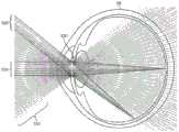
- light
- waveguide
- planar waveguide
- grating
- ope
- Prior art date
- Legal status (The legal status is an assumption and is not a legal conclusion. Google has not performed a legal analysis and makes no representation as to the accuracy of the status listed.)
- Active
Links
Images


Classifications
- G—PHYSICS
- G02—OPTICS
- G02B—OPTICAL ELEMENTS, SYSTEMS OR APPARATUS
- G02B27/00—Optical systems or apparatus not provided for by any of the groups G02B1/00 - G02B26/00, G02B30/00
- G02B27/01—Head-up displays
- G02B27/017—Head mounted
- G—PHYSICS
- G02—OPTICS
- G02B—OPTICAL ELEMENTS, SYSTEMS OR APPARATUS
- G02B1/00—Optical elements characterised by the material of which they are made; Optical coatings for optical elements
- G02B1/002—Optical elements characterised by the material of which they are made; Optical coatings for optical elements made of materials engineered to provide properties not available in nature, e.g. metamaterials
- G—PHYSICS
- G02—OPTICS
- G02B—OPTICAL ELEMENTS, SYSTEMS OR APPARATUS
- G02B27/00—Optical systems or apparatus not provided for by any of the groups G02B1/00 - G02B26/00, G02B30/00
- G02B27/0018—Optical systems or apparatus not provided for by any of the groups G02B1/00 - G02B26/00, G02B30/00 with means for preventing ghost images
- G—PHYSICS
- G02—OPTICS
- G02B—OPTICAL ELEMENTS, SYSTEMS OR APPARATUS
- G02B27/00—Optical systems or apparatus not provided for by any of the groups G02B1/00 - G02B26/00, G02B30/00
- G02B27/0081—Optical systems or apparatus not provided for by any of the groups G02B1/00 - G02B26/00, G02B30/00 with means for altering, e.g. enlarging, the entrance or exit pupil
- G—PHYSICS
- G02—OPTICS
- G02B—OPTICAL ELEMENTS, SYSTEMS OR APPARATUS
- G02B27/00—Optical systems or apparatus not provided for by any of the groups G02B1/00 - G02B26/00, G02B30/00
- G02B27/01—Head-up displays
- G02B27/0101—Head-up displays characterised by optical features
- G—PHYSICS
- G02—OPTICS
- G02B—OPTICAL ELEMENTS, SYSTEMS OR APPARATUS
- G02B27/00—Optical systems or apparatus not provided for by any of the groups G02B1/00 - G02B26/00, G02B30/00
- G02B27/01—Head-up displays
- G02B27/017—Head mounted
- G02B27/0172—Head mounted characterised by optical features
- G—PHYSICS
- G02—OPTICS
- G02B—OPTICAL ELEMENTS, SYSTEMS OR APPARATUS
- G02B27/00—Optical systems or apparatus not provided for by any of the groups G02B1/00 - G02B26/00, G02B30/00
- G02B27/01—Head-up displays
- G02B27/017—Head mounted
- G02B27/0176—Head mounted characterised by mechanical features
- G—PHYSICS
- G02—OPTICS
- G02B—OPTICAL ELEMENTS, SYSTEMS OR APPARATUS
- G02B27/00—Optical systems or apparatus not provided for by any of the groups G02B1/00 - G02B26/00, G02B30/00
- G02B27/01—Head-up displays
- G02B27/0179—Display position adjusting means not related to the information to be displayed
- G—PHYSICS
- G02—OPTICS
- G02B—OPTICAL ELEMENTS, SYSTEMS OR APPARATUS
- G02B27/00—Optical systems or apparatus not provided for by any of the groups G02B1/00 - G02B26/00, G02B30/00
- G02B27/10—Beam splitting or combining systems
- G02B27/1086—Beam splitting or combining systems operating by diffraction only
- G—PHYSICS
- G02—OPTICS
- G02B—OPTICAL ELEMENTS, SYSTEMS OR APPARATUS
- G02B27/00—Optical systems or apparatus not provided for by any of the groups G02B1/00 - G02B26/00, G02B30/00
- G02B27/28—Optical systems or apparatus not provided for by any of the groups G02B1/00 - G02B26/00, G02B30/00 for polarising
- G02B27/283—Optical systems or apparatus not provided for by any of the groups G02B1/00 - G02B26/00, G02B30/00 for polarising used for beam splitting or combining
- G—PHYSICS
- G02—OPTICS
- G02B—OPTICAL ELEMENTS, SYSTEMS OR APPARATUS
- G02B27/00—Optical systems or apparatus not provided for by any of the groups G02B1/00 - G02B26/00, G02B30/00
- G02B27/30—Collimators
- G—PHYSICS
- G02—OPTICS
- G02B—OPTICAL ELEMENTS, SYSTEMS OR APPARATUS
- G02B5/00—Optical elements other than lenses
- G02B5/18—Diffraction gratings
- G02B5/1814—Diffraction gratings structurally combined with one or more further optical elements, e.g. lenses, mirrors, prisms or other diffraction gratings
- G02B5/1819—Plural gratings positioned on the same surface, e.g. array of gratings
- G02B5/1823—Plural gratings positioned on the same surface, e.g. array of gratings in an overlapping or superposed manner
- G—PHYSICS
- G02—OPTICS
- G02B—OPTICAL ELEMENTS, SYSTEMS OR APPARATUS
- G02B5/00—Optical elements other than lenses
- G02B5/18—Diffraction gratings
- G02B5/1847—Manufacturing methods
- G02B5/1857—Manufacturing methods using exposure or etching means, e.g. holography, photolithography, exposure to electron or ion beams
- G—PHYSICS
- G02—OPTICS
- G02B—OPTICAL ELEMENTS, SYSTEMS OR APPARATUS
- G02B5/00—Optical elements other than lenses
- G02B5/18—Diffraction gratings
- G02B5/1866—Transmission gratings characterised by their structure, e.g. step profile, contours of substrate or grooves, pitch variations, materials
- G—PHYSICS
- G02—OPTICS
- G02B—OPTICAL ELEMENTS, SYSTEMS OR APPARATUS
- G02B5/00—Optical elements other than lenses
- G02B5/18—Diffraction gratings
- G02B5/1866—Transmission gratings characterised by their structure, e.g. step profile, contours of substrate or grooves, pitch variations, materials
- G02B5/1871—Transmissive phase gratings
- G—PHYSICS
- G02—OPTICS
- G02B—OPTICAL ELEMENTS, SYSTEMS OR APPARATUS
- G02B5/00—Optical elements other than lenses
- G02B5/30—Polarising elements
- G02B5/3025—Polarisers, i.e. arrangements capable of producing a definite output polarisation state from an unpolarised input state
- G—PHYSICS
- G02—OPTICS
- G02B—OPTICAL ELEMENTS, SYSTEMS OR APPARATUS
- G02B6/00—Light guides; Structural details of arrangements comprising light guides and other optical elements, e.g. couplings
- G02B6/0001—Light guides; Structural details of arrangements comprising light guides and other optical elements, e.g. couplings specially adapted for lighting devices or systems
- G02B6/0011—Light guides; Structural details of arrangements comprising light guides and other optical elements, e.g. couplings specially adapted for lighting devices or systems the light guides being planar or of plate-like form
- G02B6/0013—Means for improving the coupling-in of light from the light source into the light guide
- G02B6/0015—Means for improving the coupling-in of light from the light source into the light guide provided on the surface of the light guide or in the bulk of it
- G02B6/0016—Grooves, prisms, gratings, scattering particles or rough surfaces
- G—PHYSICS
- G02—OPTICS
- G02B—OPTICAL ELEMENTS, SYSTEMS OR APPARATUS
- G02B6/00—Light guides; Structural details of arrangements comprising light guides and other optical elements, e.g. couplings
- G02B6/0001—Light guides; Structural details of arrangements comprising light guides and other optical elements, e.g. couplings specially adapted for lighting devices or systems
- G02B6/0011—Light guides; Structural details of arrangements comprising light guides and other optical elements, e.g. couplings specially adapted for lighting devices or systems the light guides being planar or of plate-like form
- G02B6/0013—Means for improving the coupling-in of light from the light source into the light guide
- G02B6/0023—Means for improving the coupling-in of light from the light source into the light guide provided by one optical element, or plurality thereof, placed between the light guide and the light source, or around the light source
- G—PHYSICS
- G02—OPTICS
- G02B—OPTICAL ELEMENTS, SYSTEMS OR APPARATUS
- G02B6/00—Light guides; Structural details of arrangements comprising light guides and other optical elements, e.g. couplings
- G02B6/0001—Light guides; Structural details of arrangements comprising light guides and other optical elements, e.g. couplings specially adapted for lighting devices or systems
- G02B6/0011—Light guides; Structural details of arrangements comprising light guides and other optical elements, e.g. couplings specially adapted for lighting devices or systems the light guides being planar or of plate-like form
- G02B6/0033—Means for improving the coupling-out of light from the light guide
- G02B6/0035—Means for improving the coupling-out of light from the light guide provided on the surface of the light guide or in the bulk of it
- G02B6/0036—2-D arrangement of prisms, protrusions, indentations or roughened surfaces
- G—PHYSICS
- G02—OPTICS
- G02B—OPTICAL ELEMENTS, SYSTEMS OR APPARATUS
- G02B6/00—Light guides; Structural details of arrangements comprising light guides and other optical elements, e.g. couplings
- G02B6/0001—Light guides; Structural details of arrangements comprising light guides and other optical elements, e.g. couplings specially adapted for lighting devices or systems
- G02B6/0011—Light guides; Structural details of arrangements comprising light guides and other optical elements, e.g. couplings specially adapted for lighting devices or systems the light guides being planar or of plate-like form
- G02B6/0033—Means for improving the coupling-out of light from the light guide
- G02B6/0035—Means for improving the coupling-out of light from the light guide provided on the surface of the light guide or in the bulk of it
- G02B6/0038—Linear indentations or grooves, e.g. arc-shaped grooves or meandering grooves, extending over the full length or width of the light guide
- G—PHYSICS
- G02—OPTICS
- G02B—OPTICAL ELEMENTS, SYSTEMS OR APPARATUS
- G02B6/00—Light guides; Structural details of arrangements comprising light guides and other optical elements, e.g. couplings
- G02B6/0001—Light guides; Structural details of arrangements comprising light guides and other optical elements, e.g. couplings specially adapted for lighting devices or systems
- G02B6/0011—Light guides; Structural details of arrangements comprising light guides and other optical elements, e.g. couplings specially adapted for lighting devices or systems the light guides being planar or of plate-like form
- G02B6/0033—Means for improving the coupling-out of light from the light guide
- G02B6/005—Means for improving the coupling-out of light from the light guide provided by one optical element, or plurality thereof, placed on the light output side of the light guide
- G—PHYSICS
- G02—OPTICS
- G02B—OPTICAL ELEMENTS, SYSTEMS OR APPARATUS
- G02B6/00—Light guides; Structural details of arrangements comprising light guides and other optical elements, e.g. couplings
- G02B6/0001—Light guides; Structural details of arrangements comprising light guides and other optical elements, e.g. couplings specially adapted for lighting devices or systems
- G02B6/0011—Light guides; Structural details of arrangements comprising light guides and other optical elements, e.g. couplings specially adapted for lighting devices or systems the light guides being planar or of plate-like form
- G02B6/0075—Arrangements of multiple light guides
- G02B6/0076—Stacked arrangements of multiple light guides of the same or different cross-sectional area
- G—PHYSICS
- G02—OPTICS
- G02B—OPTICAL ELEMENTS, SYSTEMS OR APPARATUS
- G02B6/00—Light guides; Structural details of arrangements comprising light guides and other optical elements, e.g. couplings
- G02B6/24—Coupling light guides
- G02B6/26—Optical coupling means
- G02B6/28—Optical coupling means having data bus means, i.e. plural waveguides interconnected and providing an inherently bidirectional system by mixing and splitting signals
- G02B6/293—Optical coupling means having data bus means, i.e. plural waveguides interconnected and providing an inherently bidirectional system by mixing and splitting signals with wavelength selective means
- G02B6/29304—Optical coupling means having data bus means, i.e. plural waveguides interconnected and providing an inherently bidirectional system by mixing and splitting signals with wavelength selective means operating by diffraction, e.g. grating
- G02B6/29316—Light guides comprising a diffractive element, e.g. grating in or on the light guide such that diffracted light is confined in the light guide
- G02B6/29325—Light guides comprising a diffractive element, e.g. grating in or on the light guide such that diffracted light is confined in the light guide of the slab or planar or plate like form, i.e. confinement in a single transverse dimension only
- G—PHYSICS
- G02—OPTICS
- G02B—OPTICAL ELEMENTS, SYSTEMS OR APPARATUS
- G02B6/00—Light guides; Structural details of arrangements comprising light guides and other optical elements, e.g. couplings
- G02B6/24—Coupling light guides
- G02B6/26—Optical coupling means
- G02B6/34—Optical coupling means utilising prism or grating
- G—PHYSICS
- G02—OPTICS
- G02B—OPTICAL ELEMENTS, SYSTEMS OR APPARATUS
- G02B7/00—Mountings, adjusting means, or light-tight connections, for optical elements
- G02B7/008—Mountings, adjusting means, or light-tight connections, for optical elements with means for compensating for changes in temperature or for controlling the temperature; thermal stabilisation
- G—PHYSICS
- G02—OPTICS
- G02C—SPECTACLES; SUNGLASSES OR GOGGLES INSOFAR AS THEY HAVE THE SAME FEATURES AS SPECTACLES; CONTACT LENSES
- G02C11/00—Non-optical adjuncts; Attachment thereof
- G02C11/10—Electronic devices other than hearing aids
- G—PHYSICS
- G02—OPTICS
- G02C—SPECTACLES; SUNGLASSES OR GOGGLES INSOFAR AS THEY HAVE THE SAME FEATURES AS SPECTACLES; CONTACT LENSES
- G02C5/00—Constructions of non-optical parts
- G02C5/14—Side-members
- G02C5/16—Side-members resilient or with resilient parts
- G—PHYSICS
- G06—COMPUTING OR CALCULATING; COUNTING
- G06F—ELECTRIC DIGITAL DATA PROCESSING
- G06F1/00—Details not covered by groups G06F3/00 - G06F13/00 and G06F21/00
- G06F1/16—Constructional details or arrangements
- G06F1/1613—Constructional details or arrangements for portable computers
- G06F1/163—Wearable computers, e.g. on a belt
- G—PHYSICS
- G06—COMPUTING OR CALCULATING; COUNTING
- G06F—ELECTRIC DIGITAL DATA PROCESSING
- G06F1/00—Details not covered by groups G06F3/00 - G06F13/00 and G06F21/00
- G06F1/16—Constructional details or arrangements
- G06F1/20—Cooling means
- G06F1/203—Cooling means for portable computers, e.g. for laptops
- G—PHYSICS
- G06—COMPUTING OR CALCULATING; COUNTING
- G06F—ELECTRIC DIGITAL DATA PROCESSING
- G06F1/00—Details not covered by groups G06F3/00 - G06F13/00 and G06F21/00
- G06F1/16—Constructional details or arrangements
- G06F1/20—Cooling means
- G06F1/206—Cooling means comprising thermal management
- G—PHYSICS
- G06—COMPUTING OR CALCULATING; COUNTING
- G06F—ELECTRIC DIGITAL DATA PROCESSING
- G06F3/00—Input arrangements for transferring data to be processed into a form capable of being handled by the computer; Output arrangements for transferring data from processing unit to output unit, e.g. interface arrangements
- G06F3/01—Input arrangements or combined input and output arrangements for interaction between user and computer
- G06F3/011—Arrangements for interaction with the human body, e.g. for user immersion in virtual reality
- G06F3/013—Eye tracking input arrangements
- G—PHYSICS
- G06—COMPUTING OR CALCULATING; COUNTING
- G06F—ELECTRIC DIGITAL DATA PROCESSING
- G06F3/00—Input arrangements for transferring data to be processed into a form capable of being handled by the computer; Output arrangements for transferring data from processing unit to output unit, e.g. interface arrangements
- G06F3/14—Digital output to display device ; Cooperation and interconnection of the display device with other functional units
- G06F3/147—Digital output to display device ; Cooperation and interconnection of the display device with other functional units using display panels
- G—PHYSICS
- G09—EDUCATION; CRYPTOGRAPHY; DISPLAY; ADVERTISING; SEALS
- G09G—ARRANGEMENTS OR CIRCUITS FOR CONTROL OF INDICATING DEVICES USING STATIC MEANS TO PRESENT VARIABLE INFORMATION
- G09G3/00—Control arrangements or circuits, of interest only in connection with visual indicators other than cathode-ray tubes
- G09G3/001—Control arrangements or circuits, of interest only in connection with visual indicators other than cathode-ray tubes using specific devices not provided for in groups G09G3/02 - G09G3/36, e.g. using an intermediate record carrier such as a film slide; Projection systems; Display of non-alphanumerical information, solely or in combination with alphanumerical information, e.g. digital display on projected diapositive as background
- G09G3/002—Control arrangements or circuits, of interest only in connection with visual indicators other than cathode-ray tubes using specific devices not provided for in groups G09G3/02 - G09G3/36, e.g. using an intermediate record carrier such as a film slide; Projection systems; Display of non-alphanumerical information, solely or in combination with alphanumerical information, e.g. digital display on projected diapositive as background to project the image of a two-dimensional display, such as an array of light emitting or modulating elements or a CRT
- G—PHYSICS
- G09—EDUCATION; CRYPTOGRAPHY; DISPLAY; ADVERTISING; SEALS
- G09G—ARRANGEMENTS OR CIRCUITS FOR CONTROL OF INDICATING DEVICES USING STATIC MEANS TO PRESENT VARIABLE INFORMATION
- G09G3/00—Control arrangements or circuits, of interest only in connection with visual indicators other than cathode-ray tubes
- G09G3/20—Control arrangements or circuits, of interest only in connection with visual indicators other than cathode-ray tubes for presentation of an assembly of a number of characters, e.g. a page, by composing the assembly by combination of individual elements arranged in a matrix no fixed position being assigned to or needed to be assigned to the individual characters or partial characters
- G09G3/2003—Display of colours
- G—PHYSICS
- G09—EDUCATION; CRYPTOGRAPHY; DISPLAY; ADVERTISING; SEALS
- G09G—ARRANGEMENTS OR CIRCUITS FOR CONTROL OF INDICATING DEVICES USING STATIC MEANS TO PRESENT VARIABLE INFORMATION
- G09G3/00—Control arrangements or circuits, of interest only in connection with visual indicators other than cathode-ray tubes
- G09G3/20—Control arrangements or circuits, of interest only in connection with visual indicators other than cathode-ray tubes for presentation of an assembly of a number of characters, e.g. a page, by composing the assembly by combination of individual elements arranged in a matrix no fixed position being assigned to or needed to be assigned to the individual characters or partial characters
- G09G3/2007—Display of intermediate tones
- G09G3/2044—Display of intermediate tones using dithering
- H—ELECTRICITY
- H04—ELECTRIC COMMUNICATION TECHNIQUE
- H04N—PICTORIAL COMMUNICATION, e.g. TELEVISION
- H04N9/00—Details of colour television systems
- H04N9/12—Picture reproducers
- H04N9/31—Projection devices for colour picture display, e.g. using electronic spatial light modulators [ESLM]
- H04N9/3102—Projection devices for colour picture display, e.g. using electronic spatial light modulators [ESLM] using two-dimensional electronic spatial light modulators
- H—ELECTRICITY
- H04—ELECTRIC COMMUNICATION TECHNIQUE
- H04N—PICTORIAL COMMUNICATION, e.g. TELEVISION
- H04N9/00—Details of colour television systems
- H04N9/12—Picture reproducers
- H04N9/31—Projection devices for colour picture display, e.g. using electronic spatial light modulators [ESLM]
- H04N9/3141—Constructional details thereof
- H04N9/3144—Cooling systems
- H—ELECTRICITY
- H04—ELECTRIC COMMUNICATION TECHNIQUE
- H04N—PICTORIAL COMMUNICATION, e.g. TELEVISION
- H04N9/00—Details of colour television systems
- H04N9/12—Picture reproducers
- H04N9/31—Projection devices for colour picture display, e.g. using electronic spatial light modulators [ESLM]
- H04N9/3141—Constructional details thereof
- H04N9/315—Modulator illumination systems
- H04N9/3164—Modulator illumination systems using multiple light sources
- H—ELECTRICITY
- H05—ELECTRIC TECHNIQUES NOT OTHERWISE PROVIDED FOR
- H05K—PRINTED CIRCUITS; CASINGS OR CONSTRUCTIONAL DETAILS OF ELECTRIC APPARATUS; MANUFACTURE OF ASSEMBLAGES OF ELECTRICAL COMPONENTS
- H05K7/00—Constructional details common to different types of electric apparatus
- H05K7/20—Modifications to facilitate cooling, ventilating, or heating
- H05K7/20954—Modifications to facilitate cooling, ventilating, or heating for display panels
- H05K7/20963—Heat transfer by conduction from internal heat source to heat radiating structure
- B—PERFORMING OPERATIONS; TRANSPORTING
- B29—WORKING OF PLASTICS; WORKING OF SUBSTANCES IN A PLASTIC STATE IN GENERAL
- B29D—PRODUCING PARTICULAR ARTICLES FROM PLASTICS OR FROM SUBSTANCES IN A PLASTIC STATE
- B29D11/00—Producing optical elements, e.g. lenses or prisms
- B29D11/0074—Production of other optical elements not provided for in B29D11/00009- B29D11/0073
- B29D11/00769—Producing diffraction gratings
- G—PHYSICS
- G02—OPTICS
- G02B—OPTICAL ELEMENTS, SYSTEMS OR APPARATUS
- G02B27/00—Optical systems or apparatus not provided for by any of the groups G02B1/00 - G02B26/00, G02B30/00
- G02B27/01—Head-up displays
- G02B27/0101—Head-up displays characterised by optical features
- G02B2027/011—Head-up displays characterised by optical features comprising device for correcting geometrical aberrations, distortion
- G—PHYSICS
- G02—OPTICS
- G02B—OPTICAL ELEMENTS, SYSTEMS OR APPARATUS
- G02B27/00—Optical systems or apparatus not provided for by any of the groups G02B1/00 - G02B26/00, G02B30/00
- G02B27/01—Head-up displays
- G02B27/0101—Head-up displays characterised by optical features
- G02B2027/0112—Head-up displays characterised by optical features comprising device for genereting colour display
- G02B2027/0114—Head-up displays characterised by optical features comprising device for genereting colour display comprising dichroic elements
- G—PHYSICS
- G02—OPTICS
- G02B—OPTICAL ELEMENTS, SYSTEMS OR APPARATUS
- G02B27/00—Optical systems or apparatus not provided for by any of the groups G02B1/00 - G02B26/00, G02B30/00
- G02B27/01—Head-up displays
- G02B27/0101—Head-up displays characterised by optical features
- G02B2027/0118—Head-up displays characterised by optical features comprising devices for improving the contrast of the display / brillance control visibility
- G02B2027/012—Head-up displays characterised by optical features comprising devices for improving the contrast of the display / brillance control visibility comprising devices for attenuating parasitic image effects
- G—PHYSICS
- G02—OPTICS
- G02B—OPTICAL ELEMENTS, SYSTEMS OR APPARATUS
- G02B27/00—Optical systems or apparatus not provided for by any of the groups G02B1/00 - G02B26/00, G02B30/00
- G02B27/01—Head-up displays
- G02B27/0101—Head-up displays characterised by optical features
- G02B2027/0123—Head-up displays characterised by optical features comprising devices increasing the field of view
- G02B2027/0125—Field-of-view increase by wavefront division
- G—PHYSICS
- G02—OPTICS
- G02B—OPTICAL ELEMENTS, SYSTEMS OR APPARATUS
- G02B27/00—Optical systems or apparatus not provided for by any of the groups G02B1/00 - G02B26/00, G02B30/00
- G02B27/01—Head-up displays
- G02B27/0101—Head-up displays characterised by optical features
- G02B2027/014—Head-up displays characterised by optical features comprising information/image processing systems
- G—PHYSICS
- G02—OPTICS
- G02B—OPTICAL ELEMENTS, SYSTEMS OR APPARATUS
- G02B27/00—Optical systems or apparatus not provided for by any of the groups G02B1/00 - G02B26/00, G02B30/00
- G02B27/01—Head-up displays
- G02B27/017—Head mounted
- G02B27/0172—Head mounted characterised by optical features
- G02B2027/0174—Head mounted characterised by optical features holographic
- G—PHYSICS
- G02—OPTICS
- G02B—OPTICAL ELEMENTS, SYSTEMS OR APPARATUS
- G02B27/00—Optical systems or apparatus not provided for by any of the groups G02B1/00 - G02B26/00, G02B30/00
- G02B27/01—Head-up displays
- G02B27/017—Head mounted
- G02B2027/0178—Eyeglass type
- G—PHYSICS
- G09—EDUCATION; CRYPTOGRAPHY; DISPLAY; ADVERTISING; SEALS
- G09G—ARRANGEMENTS OR CIRCUITS FOR CONTROL OF INDICATING DEVICES USING STATIC MEANS TO PRESENT VARIABLE INFORMATION
- G09G2320/00—Control of display operating conditions
- G09G2320/02—Improving the quality of display appearance
- G09G2320/0233—Improving the luminance or brightness uniformity across the screen
- G—PHYSICS
- G09—EDUCATION; CRYPTOGRAPHY; DISPLAY; ADVERTISING; SEALS
- G09G—ARRANGEMENTS OR CIRCUITS FOR CONTROL OF INDICATING DEVICES USING STATIC MEANS TO PRESENT VARIABLE INFORMATION
- G09G2330/00—Aspects of power supply; Aspects of display protection and defect management
- G09G2330/04—Display protection
- G09G2330/045—Protection against panel overheating
- G—PHYSICS
- G09—EDUCATION; CRYPTOGRAPHY; DISPLAY; ADVERTISING; SEALS
- G09G—ARRANGEMENTS OR CIRCUITS FOR CONTROL OF INDICATING DEVICES USING STATIC MEANS TO PRESENT VARIABLE INFORMATION
- G09G2340/00—Aspects of display data processing
- G09G2340/04—Changes in size, position or resolution of an image
- G09G2340/0464—Positioning
Landscapes
- Physics & Mathematics (AREA)
- Engineering & Computer Science (AREA)
- General Physics & Mathematics (AREA)
- Optics & Photonics (AREA)
- Theoretical Computer Science (AREA)
- General Engineering & Computer Science (AREA)
- Computer Hardware Design (AREA)
- Human Computer Interaction (AREA)
- Health & Medical Sciences (AREA)
- Ophthalmology & Optometry (AREA)
- Multimedia (AREA)
- Signal Processing (AREA)
- Manufacturing & Machinery (AREA)
- Microelectronics & Electronic Packaging (AREA)
- General Health & Medical Sciences (AREA)
- Otolaryngology (AREA)
- Acoustics & Sound (AREA)
- Thermal Sciences (AREA)
- Mechanical Engineering (AREA)
- Diffracting Gratings Or Hologram Optical Elements (AREA)
- Optical Integrated Circuits (AREA)
- Lenses (AREA)
- Optical Filters (AREA)
- Holo Graphy (AREA)
- Polarising Elements (AREA)
- Developing Agents For Electrophotography (AREA)
- Measuring Pulse, Heart Rate, Blood Pressure Or Blood Flow (AREA)
- Controls And Circuits For Display Device (AREA)
Abstract
Translated fromChinese
Description
Translated fromChinese相关申请的交叉引用CROSS-REFERENCE TO RELATED APPLICATIONS
本申请要求如下申请的优先权:2016年8月22日提交的美国临时专利申请No.62/377,831;2017年1月18日提交的美国临时专利申请No.62/447,608;2017年1月23日提交的美国临时专利申请No.62/449,524;2017年5月23日提交的美国临时专利申请No.62/509,969;2017年6月14日提交的美国临时专利申请No.62/519,536;2017年6月19日提交的美国临时专利申请No.62/521,889,其公开内容为了所有目的通过引用整体并入本文。This application claims priority to: US Provisional Patent Application No. 62/377,831, filed August 22, 2016; US Provisional Patent Application No. 62/447,608, filed January 18, 2017; January 23, 2017 US Provisional Patent Application No. 62/449,524, filed May 23, 2017; US Provisional Patent Application No. 62/519,536, filed June 14, 2017; US Provisional Patent Application No. 62/521,889, filed June 19, 2009, the disclosure of which is incorporated herein by reference in its entirety for all purposes.
背景技术Background technique
现代计算和显示技术促进了用于所谓的“虚拟现实”或“增强现实”体验的系统的发展,其中数字再现图像或其部分以它们看起来是或者可以被感知为真实的方式呈现给用户。虚拟现实或“VR”场景通常涉及呈现数字或虚拟图像信息而对其它实际的真实世界视觉输入不透明;增强现实或“AR”场景通常涉及呈现数字或虚拟图像信息,作为对用户周围的实际世界的可视化的增强。Modern computing and display technologies have facilitated the development of systems for so-called "virtual reality" or "augmented reality" experiences, in which digitally reproduced images or parts thereof are presented to the user in such a way that they appear or can be perceived as real. Virtual reality or "VR" scenes typically involve the presentation of digital or virtual image information that is opaque to other actual real-world visual input; augmented reality or "AR" scenes typically involve the presentation of digital or virtual image information as a reflection of the real world around the user. Visualization enhancements.
尽管在这些显示技术方面取得了进步,但是在本领域中需要与增强现实系统(尤其是显示系统)相关的改进方法和系统。Despite advances in these display technologies, there is a need in the art for improved methods and systems related to augmented reality systems, particularly display systems.
发明内容SUMMARY OF THE INVENTION
本公开涉及虚拟现实和增强现实成像和可视化系统。本公开一般涉及与包括可穿戴显示器的投影显示系统相关的方法和系统。更具体地,本公开的实施例提供用于减少投影显示系统中的光学伪像的方法和系统。本公开适用于计算机视觉和图像显示系统中的各种应用。The present disclosure relates to virtual reality and augmented reality imaging and visualization systems. The present disclosure generally relates to methods and systems related to projection display systems including wearable displays. More specifically, embodiments of the present disclosure provide methods and systems for reducing optical artifacts in projection display systems. The present disclosure is applicable to various applications in computer vision and image display systems.
根据一些实施例,一种光学装置包括以下:框架,其限定一对眼孔并包括被配置为在光学装置的用户的耳朵上方延伸的一对臂;温度监视系统,其被配置为监视框架内的热分布;显示组件,其被配置为向光学装置的用户显示内容;以及处理器,其被配置为从温度监视系统接收温度数据,并基于框架内的热分布中的变化来调节显示组件的输出。According to some embodiments, an optical device includes the following: a frame defining a pair of eyelets and including a pair of arms configured to extend over an ear of a user of the optical device; a temperature monitoring system configured to monitor within the frame a display assembly configured to display content to a user of the optical device; and a processor configured to receive temperature data from a temperature monitoring system and adjust the thermal distribution of the display assembly based on changes in the thermal distribution within the frame output.
根据一些实施例,一种光学装置包括以下:框架组件,其包括被配置为在光学装置的用户的耳朵上方延伸的一对臂,并限定第一眼孔和第二眼孔;第一和第二投影仪,其耦合到框架组件;衍射光学器件,其被配置为接收由第一和第二投影仪发射的光并将光朝向用户的眼睛取向;以及处理器,其被配置为根据光学装置的热分布来移动由第一和第二投影仪投影的内容。According to some embodiments, an optical device includes the following: a frame assembly including a pair of arms configured to extend over an ear of a user of the optical device and defining first and second eyelets; first and second eyelets two projectors coupled to the frame assembly; diffractive optics configured to receive light emitted by the first and second projectors and to direct the light toward the user's eye; and a processor configured to respond to the optics the heat distribution to move the content projected by the first and second projectors.
根据一些实施例,一种光学装置包括以下:框架组件,其包括通过前带连接在一起的一对臂以及热分布系统,该一对臂被配置为接触光学装置的用户的耳朵,该热分布系统用于将由光学装置生成的热导向光学装置的散热区域;电子装置,其通过热分布系统与框架组件热接触,该热分布系统被配置为将由多个电子装置发出的热分布到该一对臂和前带;显示组件;以及处理器,其被配置为根据多个电子装置的温度变化来调节显示组件的操作。According to some embodiments, an optical device includes the following: a frame assembly including a pair of arms connected together by a front strap and a heat distribution system, the pair of arms being configured to contact an ear of a user of the optical device, the heat distribution a system for directing heat generated by the optical device to a heat sink area of the optical device; an electronic device in thermal contact with the frame assembly by a heat distribution system configured to distribute heat emitted by the plurality of electronic devices to the pair an arm and a front strap; a display assembly; and a processor configured to adjust operation of the display assembly according to temperature changes of the plurality of electronic devices.
根据本发明的实施例,提供了一种伪像减轻系统。该伪像减轻系统包括投影仪组件、光学耦合到投影仪组件的一组成像光学器件,以及光学耦合到该组成像光学器件的目镜。该目镜包括内耦合界面。伪像减轻系统还包括设置在该组成像光学器件和目镜之间的伪像防止元件。伪像防止元件包括线偏振器、与线偏振器相邻设置的第一四分之一波片,以及与第一四分之一波片相邻设置的颜色选择部件。According to an embodiment of the present invention, an artifact mitigation system is provided. The artifact mitigation system includes a projector assembly, a set of imaging optics optically coupled to the projector assembly, and an eyepiece optically coupled to the set of imaging optics. The eyepiece includes an in-coupling interface. The artifact mitigation system also includes an artifact prevention element disposed between the set of imaging optics and the eyepiece. The artifact preventing element includes a linear polarizer, a first quarter-wave plate disposed adjacent to the linear polarizer, and a color selection member disposed adjacent to the first quarter-wave plate.
根据本发明的另一实施例,提供了一种伪像减轻系统。该伪像减轻系统包括投影仪组件、光学耦合到投影仪组件的一组成像光学器件,以及光学耦合到该组成像光学器件的目镜。该目镜包括具有第一组内耦合衍射元件和第二组内耦合衍射元件的内耦合区域。伪像减轻系统进一步包括设置在该组成像光学器件和目镜之间的一组滤色器。该组滤色器包括与第一组内耦合衍射元件相邻设置的第一滤光器和与第二组内耦合衍射元件相邻设置的第二滤光器。According to another embodiment of the present invention, an artifact mitigation system is provided. The artifact mitigation system includes a projector assembly, a set of imaging optics optically coupled to the projector assembly, and an eyepiece optically coupled to the set of imaging optics. The eyepiece includes an incoupling region having a first set of incoupling diffractive elements and a second set of incoupling diffractive elements. The artifact mitigation system further includes a set of color filters disposed between the set of imaging optics and the eyepiece. The set of color filters includes a first filter disposed adjacent to the first set of in-coupling diffractive elements and a second filter disposed adjacent to the second set of in-coupling diffractive elements.
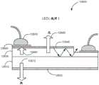
根据本发明的特定实施例,提供了一种投影仪组件。该投影仪组件包括偏振分束器(PBS)、与PBS相邻设置的一组空间移位光源,以及与PBS相邻设置的准直器。该组空间移位光源可包括具有不同颜色的一组三个LED。在一些实施例中,该组空间移位光源与PBS的第一侧相邻。准直器可以与PBS的邻近第一侧的第二侧相邻。According to certain embodiments of the present invention, a projector assembly is provided. The projector assembly includes a polarizing beam splitter (PBS), a set of spatially shifted light sources positioned adjacent to the PBS, and a collimator positioned adjacent to the PBS. The set of spatially displaced light sources may comprise a set of three LEDs of different colors. In some embodiments, the set of spatially displaced light sources is adjacent to the first side of the PBS. The collimator may be adjacent to a second side of the PBS adjacent to the first side.
投影仪组件还包括与PBS相邻设置的显示面板(例如,LCOS面板)、与PBS相邻设置的圆偏振器,以及与PBS相邻设置的一组成像光学器件。圆偏振器可以设置在PBS和该组成像光学器件之间。显示面板可以与PBS的第三侧相邻设置,其中第三侧与第一侧相邻并且与第二侧相对。此外,该组成像光学器件可以与PBS的第四侧相邻设置,其中第四侧与第一侧相对。The projector assembly also includes a display panel (eg, an LCOS panel) positioned adjacent to the PBS, a circular polarizer positioned adjacent to the PBS, and a set of imaging optics positioned adjacent to the PBS. A circular polarizer can be placed between the PBS and the set of imaging optics. The display panel may be positioned adjacent to a third side of the PBS, wherein the third side is adjacent to the first side and opposite the second side. Additionally, the set of imaging optics may be positioned adjacent a fourth side of the PBS, wherein the fourth side is opposite the first side.
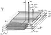
在一个实施例中,该组成像光学器件在内耦合界面处形成显示面板的图像。在该实施例中,投影仪组件包括位于内耦合界面处的目镜。该组空间移位光源中的每个光源可以在内耦合界面的单独部分处成像。目镜可包括多个波导层。In one embodiment, the set of imaging optics forms an image of the display panel at the in-coupling interface. In this embodiment, the projector assembly includes an eyepiece at the incoupling interface. Each light source in the set of spatially displaced light sources can be imaged at a separate portion of the incoupling interface. The eyepiece may include multiple waveguide layers.
本发明的一些实施例提供了使用在目镜中层叠在一起的一个或多个波导将图像投影到用户眼睛的方法和系统。波导可包括设置在波导的一个或多个表面内或之上的一个或多个光栅和/或衍射元件。Some embodiments of the present invention provide methods and systems for projecting an image to a user's eye using one or more waveguides stacked together in an eyepiece. The waveguide may include one or more gratings and/or diffractive elements disposed in or on one or more surfaces of the waveguide.
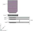
在一些实施例中,提供了用于观察投影图像的波导。波导可包括用于引导光的基板。波导还可以包括内耦合衍射元件,该内耦合衍射元件设置在基板内或基板上并且配置为将与投影图像相关的内耦合光衍射到基板中。波导可进一步包括第一光栅,该第一光栅设置在基板内或基板上并被配置为操控来自内耦合衍射元件的衍射的内耦合光,以便将投影图像倍增并将倍增的投影图像引导到第二光栅。在一些实施例中,波导包括第二光栅,该第二光栅设置在基板内或基板上,并被配置为将操控的衍射内耦合光从波导的外耦合出。在一些实施例中,第一光栅和第二光栅占据波导的相同区域。In some embodiments, a waveguide for viewing projected images is provided. The waveguide may include a substrate for guiding light. The waveguide may also include an in-coupling diffractive element disposed in or on the substrate and configured to diffract in-coupled light associated with the projected image into the substrate. The waveguide may further include a first grating disposed in or on the substrate and configured to manipulate diffracted in-coupled light from the in-coupling diffractive element to multiply the projected image and direct the multiplied projected image to the first grating. Two gratings. In some embodiments, the waveguide includes a second grating disposed in or on the substrate and configured to couple the steered diffracted in-coupled light out of the waveguide. In some embodiments, the first grating and the second grating occupy the same area of the waveguide.
在一些实施例中,第一光栅和第二光栅设置在基板的同一侧上或同一侧内,使得第一光栅和第二光栅叠加在彼此上。在一些实施例中,第一光栅和第二光栅设置在基板的不同侧上或不同侧内。在一些实施例中,波导可以包括第三光栅,该第三光栅设置在基板内或基板上,并且被配置为操控来自内耦合衍射元件的衍射的内耦合光,以便将投影图像倍增并将倍增的投影图像引导到第二光栅。在一些实施例中,第一光栅被配置为在第一方向中将倍增的投影图像引导到第二光栅。在一些实施例中,第三光栅被配置为在第二方向中将倍增的投影图像引导到第二光栅,第二方向与第一方向相反。在一些实施例中,第一光栅、第二光栅和第三光栅设置在基板的同一侧上或同一侧内,使得第一光栅、第二光栅和第三光栅叠加在彼此上。在一些实施例中,第一光栅和第三光栅设置在基板的同一侧上或同一侧内,使得第一光栅和第三光栅叠加在彼此上。在一些实施例中,第二光栅设置在基板的相对侧上或相对内。In some embodiments, the first grating and the second grating are disposed on or within the same side of the substrate such that the first and second gratings are superimposed on each other. In some embodiments, the first grating and the second grating are disposed on or in different sides of the substrate. In some embodiments, the waveguide may include a third grating disposed in or on the substrate and configured to manipulate diffracted in-coupled light from the in-coupling diffractive element in order to multiply and multiply the projected image The projected image is directed to the second grating. In some embodiments, the first grating is configured to direct the multiplied projected image to the second grating in the first direction. In some embodiments, the third grating is configured to direct the multiplied projected image to the second grating in a second direction opposite to the first direction. In some embodiments, the first grating, the second grating and the third grating are disposed on or within the same side of the substrate such that the first, second and third gratings are superimposed on each other. In some embodiments, the first grating and the third grating are disposed on or within the same side of the substrate such that the first and third gratings are superimposed on each other. In some embodiments, the second grating is disposed on or in opposite sides of the substrate.
在一些实施例中,提供了一种用于观察投影图像的目镜。目镜可以包括在分层布置中耦合在一起的多个波导。在一些实施例中,多个波导中的每个波导包括基板、内耦合衍射元件、第一光栅和第二光栅。In some embodiments, an eyepiece for viewing projected images is provided. The eyepiece may include multiple waveguides coupled together in a layered arrangement. In some embodiments, each waveguide of the plurality of waveguides includes a substrate, an in-coupling diffractive element, a first grating, and a second grating.
在一些实施例中,提供了用于观察投影图像的波导。波导可包括用于引导光的基板。波导还可以包括内耦合衍射元件,该内耦合衍射元件设置在基板内或基板上,并且配置为在至少第一方向和第二方向中将与投影图像有关的内耦合光衍射到基板中。波导可以进一步包括第一光栅,该第一光栅设置在基板内或基板上,并且被配置为操控在第一方向中衍射的内耦合光,以便将投影图像倍增并将第一倍增的投影图像引导到第三光栅。在一些实施例中,波导包括第二光栅,该第二光栅设置在基板内或基板上,并且被配置为操控在第二方向中衍射的内耦合光,以便将投影图像倍增并将第二倍增的投影图像引导到第三光栅。在一些实施例中,第三光栅设置在基板内或基板上,并且被配置为将第一倍增的投影图像的至少一部分从波导外耦合出,并且将第二倍增的投影图像的至少一部分从波导外耦合出。In some embodiments, a waveguide for viewing projected images is provided. The waveguide may include a substrate for guiding light. The waveguide may also include an in-coupling diffractive element disposed in or on the substrate and configured to diffract in-coupled light associated with the projected image into the substrate in at least the first and second directions. The waveguide may further include a first grating disposed in or on the substrate and configured to manipulate the diffracted in-coupled light in the first direction to multiply the projected image and direct the first multiplied projected image to the third grating. In some embodiments, the waveguide includes a second grating disposed in or on the substrate and configured to manipulate the in-coupled light diffracted in the second direction to multiply the projected image and multiply the second The projected image is directed to the third grating. In some embodiments, the third grating is disposed in or on the substrate and is configured to outcouple at least a portion of the first multiplied projected image out of the waveguide and at least a portion of the second multiplied projected image from the waveguide Outcoupling out.
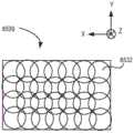
在一些实施例中,内耦合衍射元件被配置为在第三方向中将与投影图像相关的内耦合光衍射到基板中。在一些实施例中,第三光栅被配置为在第三方向中将衍射的内耦合光的至少一部分从波导外耦合出。在一些实施例中,第一方向基本上与第二方向相反。在一些实施例中,第三方向基本上正交于第一方向和第二方向。在一些实施例中,内耦合衍射元件包括彼此正交的两个叠加衍射光栅。在一些实施例中,第一方向与第二方向形成120度角。在一些实施例中,第三方向与第一方向和第二方向中的每一个方向形成60度角。在一些实施例中,内耦合衍射元件包括以六边形网格布置的多个岛。在一些实施例中,多个波导可以在分层布置中耦合在一起。In some embodiments, the in-coupling diffractive element is configured to diffract in-coupled light associated with the projected image into the substrate in the third direction. In some embodiments, the third grating is configured to outcouple at least a portion of the diffracted in-coupled light out of the waveguide in the third direction. In some embodiments, the first direction is substantially opposite to the second direction. In some embodiments, the third direction is substantially orthogonal to the first and second directions. In some embodiments, the in-coupling diffractive element comprises two superimposed diffraction gratings orthogonal to each other. In some embodiments, the first direction and the second direction form an angle of 120 degrees. In some embodiments, the third direction forms a 60-degree angle with each of the first and second directions. In some embodiments, the in-coupling diffractive element includes a plurality of islands arranged in a hexagonal grid. In some embodiments, multiple waveguides may be coupled together in a layered arrangement.
一些实施例包括在分层布置中耦合在一起的多个波导,其中多个波导中的每个波导包括:用于引导光的基板;内耦合衍射元件,其设置在基板内或基板上并且被配置为将与投影图像相关的内耦合光衍射到基板中;第一光栅,其设置在基板内或基板上,并被配置为操控来自内耦合衍射元件的衍射的内耦合光,以便将投影图像倍增并将倍增的投影图像引导到第二光栅;以及第二光栅,其设置在基板内或基板上,被配置为将所操控的衍射的内耦合光从波导外耦合出。Some embodiments include a plurality of waveguides coupled together in a layered arrangement, wherein each waveguide in the plurality of waveguides includes: a substrate for directing light; an in-coupling diffractive element disposed in or on the substrate and by configured to diffract in-coupled light associated with the projected image into the substrate; a first grating disposed in or on the substrate and configured to manipulate the diffracted in-coupled light from the in-coupling diffractive element to diffract the projected image multiplying and directing the multiplied projected image to a second grating; and a second grating disposed in or on the substrate and configured to outcouple the manipulated diffracted in-coupled light out of the waveguide.
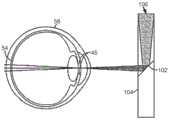
根据本发明的实施例,提供了一种用于将图像投影到观察者的眼睛的目镜。该目镜包括具有前表面和后表面的平面波导,该平面波导被配置为传播第一波长范围内的光。目镜还包括光栅,该光栅耦合到波导的后表面并且被配置为将在波导中传播的光的第一部分朝向第一方向衍射出波导的平面并且将在波导中传播的光的第二部分朝向与第一方向相反的第二方向衍射出波导的平面。目镜进一步包括波长选择反射器,该波长选择反射器耦合到波导的前表面并且被配置为反射第一波长范围内的光并透射第一波长范围之外的光,使得波长选择反射器将光的第二部分的至少一部分朝向第一方向反射回来。According to an embodiment of the present invention, there is provided an eyepiece for projecting an image to an eye of an observer. The eyepiece includes a planar waveguide having a front surface and a rear surface, the planar waveguide configured to propagate light in a first wavelength range. The eyepiece also includes a grating coupled to the rear surface of the waveguide and configured to diffract a first portion of light propagating in the waveguide out of the plane of the waveguide toward a first direction and to diffract a second portion of light propagating in the waveguide toward and A second direction opposite the first direction diffracts out of the plane of the waveguide. The eyepiece further includes a wavelength selective reflector coupled to the front surface of the waveguide and configured to reflect light within the first wavelength range and transmit light outside the first wavelength range, such that the wavelength selective reflector converts light of the light At least a portion of the second portion is reflected back toward the first direction.
根据本发明的另一实施例,提供了一种用于将图像投影到观察者的眼睛的目镜。目镜包括具有第一前表面和第一后表面的第一平面波导,以及基本上平行于第一平面波导并在第一平面波导之前设置的第二平面波导。第一平面波导被配置为传播第一波长范围内的第一光。第二平面波导具有第二前表面和第二后表面,并且被配置为传播第二波长范围内的第二光。目镜还包括第三平面波导,其基本上平行于第二平面波导并在第二平面波导的前面设置。第三平面波导具有第三前表面和第三后表面,并且被配置为传播第三波长范围内的第三光。目镜进一步包括第一光栅,该第一光栅耦合到第一平面波导的第一后表面并且被配置为将在第一平面波导中传播的第一光的第一部分朝向第一方向衍射出第一平面波导的平面,并且将第一光的第二部分朝向与第一方向相反的第二方向衍射出第一平面波导的平面。目镜另外包括第二光栅,该第二光栅耦合到第二平面波导的第二后表面并且被配置为将在第二平面波导中传播的第二光的第一部分朝向第一方向衍射出第二平面波导的平面,并且将第二光的第二部分朝向第二方向衍射出第二平面波导的平面。目镜还包括第三光栅,该第三光栅耦合到第三平面波导的第三后表面并且被配置为将在第三平面波导中传播的第三光的第一部分朝向第一方向衍射出第三平面波导的平面,并且将第三光的第二部分朝向第二方向衍射出第三平面波导的平面。According to another embodiment of the present invention, there is provided an eyepiece for projecting an image to an eye of an observer. The eyepiece includes a first planar waveguide having a first front surface and a first rear surface, and a second planar waveguide substantially parallel to and preceding the first planar waveguide. The first planar waveguide is configured to propagate the first light in the first wavelength range. The second planar waveguide has a second front surface and a second back surface and is configured to propagate the second light in the second wavelength range. The eyepiece also includes a third planar waveguide substantially parallel to and in front of the second planar waveguide. The third planar waveguide has a third front surface and a third back surface and is configured to propagate a third light in a third wavelength range. The eyepiece further includes a first grating coupled to the first rear surface of the first planar waveguide and configured to diffract a first portion of the first light propagating in the first planar waveguide out of the first plane toward a first direction the plane of the waveguide, and diffracting the second portion of the first light out of the plane of the first planar waveguide toward a second direction opposite to the first direction. The eyepiece additionally includes a second grating coupled to the second rear surface of the second planar waveguide and configured to diffract a first portion of the second light propagating in the second planar waveguide out of the second plane toward the first direction the plane of the waveguide, and diffracting the second portion of the second light out of the plane of the second planar waveguide toward the second direction. The eyepiece also includes a third grating coupled to the third rear surface of the third planar waveguide and configured to diffract a first portion of the third light propagating in the third planar waveguide out of the third plane toward the first direction the plane of the waveguide, and diffracting the second portion of the third light out of the plane of the third plane waveguide toward the second direction.
目镜包括第一波长选择反射器,该第一波长选择反射器耦合到第一平面波导的第一前表面并且被配置为反射第一波长范围内的光并透射第一波长范围之外的光,使得第一波长选择反射器将第一光的第二部分的至少一部分朝向第一方向反射回来。目镜还包括第二波长选择反射器,该第二波长选择反射器耦合到第二平面波导的第二前表面并且被配置为反射第二波长范围内的光并透射第二波长范围之外的光,使得第二波长选择反射器将第二光的第二部分的至少一部分朝向第一方向反射回来。目镜进一步包括第三波长选择反射器,该第三波长选择反射器耦合到第三平面波导的第三前表面并且被配置为反射第三波长范围内的光并透射第三波长范围之外的光,使得第三波长选择反射器将第三光的第二部分的至少一部分朝向第一方向反射回来。the eyepiece includes a first wavelength selective reflector coupled to the first front surface of the first planar waveguide and configured to reflect light within the first wavelength range and transmit light outside the first wavelength range, The first wavelength selective reflector is caused to reflect at least a portion of the second portion of the first light back toward the first direction. The eyepiece also includes a second wavelength selective reflector coupled to the second front surface of the second planar waveguide and configured to reflect light in the second wavelength range and transmit light outside the second wavelength range , so that the second wavelength selective reflector reflects at least a portion of the second portion of the second light back toward the first direction. The eyepiece further includes a third wavelength selective reflector coupled to the third front surface of the third planar waveguide and configured to reflect light within the third wavelength range and transmit light outside the third wavelength range , so that the third wavelength selective reflector reflects at least a portion of the second portion of the third light back toward the first direction.
根据本发明的特定实施例,提供了一种用于将图像投影到观察者的眼睛的目镜。目镜包括第一平面波导,该第一平面波导具有第一前表面和第一后表面,并被配置为传播第一波长范围内的第一光。目镜还包括第二平面波导,该第二平面波导基本上平行于第一平面波导并在第一平面波导的前面设置。第二平面波导具有第二前表面和第二后表面,并且被配置为传播第二波长范围内的第二光。目镜进一步包括第三平面波导,该第三平面波导基本上平行于第二平面波导并在第二平面波导的前面设置。第三平面波导具有第三前表面和第三后表面,并且被配置为传播第三波长范围内的第三光。According to certain embodiments of the present invention, there is provided an eyepiece for projecting an image to an eye of an observer. The eyepiece includes a first planar waveguide having a first front surface and a first rear surface and configured to propagate first light in a first wavelength range. The eyepiece also includes a second planar waveguide substantially parallel to and in front of the first planar waveguide. The second planar waveguide has a second front surface and a second back surface and is configured to propagate the second light in the second wavelength range. The eyepiece further includes a third planar waveguide substantially parallel to and in front of the second planar waveguide. The third planar waveguide has a third front surface and a third back surface and is configured to propagate a third light in a third wavelength range.
另外,目镜包括第一光栅,该第一光栅耦合到第一平面波导的第一前表面并且被配置为将在第一平面波导中传播的第一光的第一部分朝向第一方向衍射出第一平面波导的平面,并将第一光的第二部分朝向与第一方向相反的第二方向衍射出第一平面波导的平面。目镜还包括第二光栅,该第二光栅耦合到第二平面波导的第二前表面并且被配置为将在第二平面波导中传播的第二光的第一部分朝向第一方向衍射出第二平面波导的平面,并且将第二光的第二部分朝向第二方向衍射出第二平面波导的平面。目镜进一步包括第三光栅,该第三光栅耦合到第三波导的第三前表面并且被配置为将在第三平面波导中传播的第三光的第一部分朝向第一方向衍射出第三平面波导的平面,并将第三光的第二部分朝向第二方向衍射出第三平面波导的平面。Additionally, the eyepiece includes a first grating coupled to the first front surface of the first planar waveguide and configured to diffract a first portion of the first light propagating in the first planar waveguide out of a first direction toward a first direction the plane of the planar waveguide, and diffracting the second portion of the first light out of the plane of the first planar waveguide toward a second direction opposite to the first direction. The eyepiece also includes a second grating coupled to the second front surface of the second planar waveguide and configured to diffract the first portion of the second light propagating in the second planar waveguide out of the second plane toward the first direction the plane of the waveguide, and diffracting the second portion of the second light out of the plane of the second planar waveguide toward the second direction. The eyepiece further includes a third grating coupled to the third front surface of the third waveguide and configured to diffract the first portion of the third light propagating in the third planar waveguide out of the third planar waveguide toward the first direction and diffracting the second part of the third light out of the plane of the third planar waveguide toward the second direction.
此外,目镜包括第一波长选择反射器,该第一波长选择反射器耦合到第二平面波导的第二后表面并且被配置为反射第一波长范围内的光并透射第一波长范围之外的光,使得第一波长选择反射器将第一光的第二部分的至少一部分朝向第一方向反射回来。目镜还包括第二波长选择反射器,该第二波长选择反射器耦合到第三平面波导的第三后表面并且被配置为反射第二波长范围内的光并透射第二波长范围之外的光,使得第二波长选择反射器将第二光的第二部分的至少一部分朝向第一方向反射回来。目镜进一步包括:前盖板,该前盖板基本上平行于第三平面波导并在第三平面波导的前面设置;以及第三波长选择反射器,其耦合到前盖板的表面。第三平面波导被配置为反射第三波长范围内的光并透射第三波长范围之外的光,使得第三波长选择反射器将第三光的第二部分的至少一部分朝向第一方向反射回来。Additionally, the eyepiece includes a first wavelength selective reflector coupled to the second rear surface of the second planar waveguide and configured to reflect light within the first wavelength range and transmit light outside the first wavelength range light such that the first wavelength selective reflector reflects at least a portion of the second portion of the first light back toward the first direction. The eyepiece also includes a second wavelength selective reflector coupled to the third rear surface of the third planar waveguide and configured to reflect light within the second wavelength range and transmit light outside the second wavelength range , so that the second wavelength selective reflector reflects at least a portion of the second portion of the second light back toward the first direction. The eyepiece further includes: a front cover plate substantially parallel to and in front of the third planar waveguide; and a third wavelength selective reflector coupled to the surface of the front cover plate. The third planar waveguide is configured to reflect light within the third wavelength range and transmit light outside the third wavelength range such that the third wavelength selective reflector reflects at least a portion of the second portion of the third light back toward the first direction .
本公开的一些实施例提供了用于改善投影显示系统的质量和均匀性的方法和系统。Some embodiments of the present disclosure provide methods and systems for improving the quality and uniformity of projection display systems.
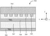
根据一些实施例,提供了一种制造具有二元光栅结构和闪耀光栅结构的组合的波导的方法。该方法包括离轴切割基板。该方法进一步包括在基板上沉积第一层。该方法进一步包括在第一层上沉积抗蚀剂层,其中抗蚀剂层包括图案。该方法进一步包括使用抗蚀剂层作为掩模来蚀刻图案中的第一层,其中图案包括第一区域和第二区域。该方法进一步包括去除抗蚀剂层。该方法进一步包括在图案的第一区域中涂覆第一聚合物层。该方法进一步包括在图案的第二区域中蚀刻基板,从而在第二区域中的基板中产生二元光栅结构。该方法进一步包括去除第一聚合物层。该方法进一步包括在图案的第二区域中涂覆第二聚合物层。该方法进一步包括在图案的第一区域中蚀刻基板,从而在第一区域中的基板中产生闪耀光栅结构。该方法进一步包括去除第二聚合物层。该方法进一步包括从基板去除第一层。According to some embodiments, a method of fabricating a waveguide having a combination of a binary grating structure and a blazed grating structure is provided. The method includes cutting the substrate off-axis. The method further includes depositing a first layer on the substrate. The method further includes depositing a resist layer on the first layer, wherein the resist layer includes a pattern. The method further includes etching the first layer in the pattern using the resist layer as a mask, wherein the pattern includes the first region and the second region. The method further includes removing the resist layer. The method further includes applying a first polymer layer in the first region of the pattern. The method further includes etching the substrate in the second region of the pattern, thereby producing a binary grating structure in the substrate in the second region. The method further includes removing the first polymer layer. The method further includes applying a second polymer layer in the second region of the pattern. The method further includes etching the substrate in the first region of the pattern, thereby producing a blazed grating structure in the substrate in the first region. The method further includes removing the second polymer layer. The method further includes removing the first layer from the substrate.
根据一些实施例,提供了一种制造具有多级二元光栅结构的波导的方法。该方法包括在第一基板上涂覆第一蚀刻停止层。该方法进一步包括在第一蚀刻停止层上添加第二基板。该方法进一步包括在第二基板上沉积第一抗蚀剂层,其中第一抗蚀剂层包括至少一个第一开口。该方法进一步包括在至少一个第一开口中的第二基板上沉积第二蚀刻停止层。该方法进一步包括从第二基板去除第一抗蚀剂层。该方法进一步包括在第二基板和第二蚀刻停止层上添加第三基板。该方法进一步包括在第三基板上沉积第二抗蚀剂层,其中第二抗蚀剂层包括至少一个第二开口。该方法进一步包括在该至少一个第二开口中的第三基板上沉积第三蚀刻停止层。该方法进一步包括从第三基板去除第二抗蚀剂层。该方法进一步包括蚀刻第二基板和第三基板,将第一基板、第一蚀刻停止层、第二蚀刻停止层和第二基板留在至少一个第一开口中,并且将第三蚀刻停止层和第三基板留在至少一个第二开口中。该方法进一步包括蚀刻第一蚀刻停止层的暴露部分、第二蚀刻停止层的暴露部分和第三蚀刻停止层,从而形成多层次二元光栅。According to some embodiments, a method of fabricating a waveguide having a multilevel binary grating structure is provided. The method includes applying a first etch stop layer on the first substrate. The method further includes adding a second substrate over the first etch stop layer. The method further includes depositing a first resist layer on the second substrate, wherein the first resist layer includes at least one first opening. The method further includes depositing a second etch stop layer on the second substrate in the at least one first opening. The method further includes removing the first resist layer from the second substrate. The method further includes adding a third substrate over the second substrate and the second etch stop layer. The method further includes depositing a second resist layer on the third substrate, wherein the second resist layer includes at least one second opening. The method further includes depositing a third etch stop layer on the third substrate in the at least one second opening. The method further includes removing the second resist layer from the third substrate. The method further includes etching the second substrate and the third substrate, leaving the first substrate, the first etch stop layer, the second etch stop layer and the second substrate in the at least one first opening, and the third etch stop layer and The third substrate remains in the at least one second opening. The method further includes etching the exposed portion of the first etch stop layer, the exposed portion of the second etch stop layer, and the third etch stop layer, thereby forming a multi-level binary grating.
根据一些实施例,提供了一种制造具有闪耀光栅结构的波导的方法。该方法包括离轴切割基板。该方法进一步包括在基板上沉积抗蚀剂层,其中抗蚀剂层包括图案。该方法进一步包括使用抗蚀剂层作为掩模在图案中蚀刻基板,从而在基板中产生闪耀光栅结构。该方法进一步包括从基板去除抗蚀剂层。According to some embodiments, a method of fabricating a waveguide having a blazed grating structure is provided. The method includes cutting the substrate off-axis. The method further includes depositing a resist layer on the substrate, wherein the resist layer includes a pattern. The method further includes etching the substrate in a pattern using the resist layer as a mask, thereby producing a blazed grating structure in the substrate. The method further includes removing the resist layer from the substrate.
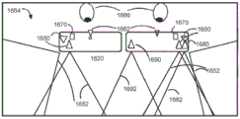
根据一些实施例,提供了一种通过目镜层操控光的方法。该方法包括在具有第一光栅结构的输入耦合光栅处接收来自光源的光,该第一光栅结构以第一组光栅参数为特征。该方法进一步包括在具有第二光栅结构的扩展光栅处接收来自输入耦合光栅的光,该第二光栅结构以第二组光栅参数为特征。该方法进一步包括在具有第三光栅结构的输出耦合光栅处接收来自扩展光栅的光,该第三光栅结构以第三组光栅参数为特征。第一光栅结构、第二光栅结构或第三光栅结构中的至少一个光栅结构具有渐变的占空比。According to some embodiments, a method of manipulating light through an eyepiece layer is provided. The method includes receiving light from a light source at an in-coupling grating having a first grating structure characterized by a first set of grating parameters. The method further includes receiving light from the in-coupling grating at an expansion grating having a second grating structure characterized by a second set of grating parameters. The method further includes receiving light from the expansion grating at an out-coupling grating having a third grating structure characterized by a third set of grating parameters. At least one of the first grating structure, the second grating structure, or the third grating structure has a graded duty cycle.
本发明的一些实施例提供用于抖动可穿戴显示装置的目镜层的方法和系统。Some embodiments of the present invention provide methods and systems for shaking an eyepiece layer of a wearable display device.
根据一些实施例,提供了一种装置。该装置包括具有第一光栅结构的输入耦合光栅,该第一光栅结构以第一组光栅参数为特征。输入耦合光栅被配置为接收来自光源的光。该装置进一步包括具有第二光栅结构的扩展光栅,该第二光栅结构以在至少两个维度上变化的第二组光栅参数为特征。第二光栅结构被配置为接收来自输入耦合光栅的光。该装置进一步包括具有第三光栅结构的输出耦合光栅,该第三光栅结构以第三组光栅参数为特征。输出耦合光栅被配置为接收来自扩展光栅的光并将光输出给观察者。According to some embodiments, an apparatus is provided. The apparatus includes an in-coupling grating having a first grating structure characterized by a first set of grating parameters. The incoupling grating is configured to receive light from the light source. The apparatus further includes an expanded grating having a second grating structure characterized by a second set of grating parameters that vary in at least two dimensions. The second grating structure is configured to receive light from the in-coupling grating. The apparatus further includes an out-coupling grating having a third grating structure characterized by a third set of grating parameters. The outcoupling grating is configured to receive light from the expanding grating and output the light to an observer.
根据一些实施例,提供了一种光学结构。光学结构包括至少部分地位于由第一维度和第二维度限定的平面中的波导层。光学结构进一步包括衍射元件,该衍射元件耦合到波导层并且可操作以在该平面中衍射光。衍射元件以至少在第一维度和第二维度中变化的一组衍射参数为特征。According to some embodiments, an optical structure is provided. The optical structure includes a waveguide layer located at least partially in a plane defined by the first dimension and the second dimension. The optical structure further includes a diffractive element coupled to the waveguide layer and operable to diffract light in the plane. The diffractive element is characterized by a set of diffractive parameters that vary in at least a first dimension and a second dimension.
通过本公开实现了优于传统技术的许多益处。例如,本发明的实施例提供了改善增强现实显示系统的可靠性和性能的方法和系统。描述了高效热扩散和散热装置,其分布和散发由于可穿戴装置的操作而生成的热。描述了用于适配可穿戴装置的显示系统的输出以考虑由不均匀的热分布或热负载的快速增加导致的光学传感器、投影仪和可穿戴显示光学器件的相对定位的变化的方法和系统。Numerous benefits over conventional techniques are realized through the present disclosure. For example, embodiments of the present invention provide methods and systems for improving the reliability and performance of augmented reality display systems. Efficient thermal diffusion and heat dissipation devices are described that distribute and dissipate heat generated due to operation of the wearable device. Methods and systems are described for adapting the output of a display system of a wearable device to account for changes in relative positioning of optical sensors, projectors, and wearable display optics caused by uneven thermal distribution or rapid increases in thermal load .
本公开的其它实施例提供了减少或消除在投影显示系统中包括鬼影图像的伪像的方法和系统。另外,本公开的实施例减少了眼疲劳,减少了由杂散光引起的伪像,并且改善了所显示的图像或视频的分辨率、ANSI对比度和整体信噪比。Other embodiments of the present disclosure provide methods and systems for reducing or eliminating artifacts including ghost images in projection display systems. Additionally, embodiments of the present disclosure reduce eye fatigue, reduce artifacts caused by stray light, and improve the resolution, ANSI contrast, and overall signal-to-noise ratio of the displayed image or video.
例如,本发明的实施例提供了通过减小目镜的尺寸和/或增加用户的视场或改善传递给用户的光的光性质(诸如亮度)来改善目镜的可扩展性以用于增强现实应用的方法和系统。当用户佩戴特定系统时,目镜的较小尺寸通常对于用户舒适性是至关重要的。由于目镜内的光出射点的宽范围和密度,本发明的实施例还使高质量图像能够投影到用户的眼睛。For example, embodiments of the present invention provide improved scalability of eyepieces for augmented reality applications by reducing the size of the eyepiece and/or increasing the user's field of view or improving the light properties (such as brightness) of the light delivered to the user method and system. The smaller size of the eyepiece is often critical for user comfort when a user wears a particular system. Embodiments of the present invention also enable high quality images to be projected onto the user's eyes due to the wide range and density of light exit points within the eyepiece.
本公开的其它实施例提供了用于在目镜层上提供光栅的方法和系统,该光栅改善了光在投影显示系统中的通路。另外,本公开的一些实施例可以提供跨投影到观察者的输出图像的光强度均匀性的增加。在一些实施例中,均匀性可以是平衡的,从而导致改进的可制造性和更大的设计灵活性。结合下文和附图更详细地描述了本公开的这些和其它实施例以及其许多优点和特征。Other embodiments of the present disclosure provide methods and systems for providing gratings on the eyepiece layer that improve the passage of light in projection display systems. Additionally, some embodiments of the present disclosure may provide increased light intensity uniformity across the output image projected to the viewer. In some embodiments, uniformity may be balanced, resulting in improved manufacturability and greater design flexibility. These and other embodiments of the present disclosure, along with its many advantages and features, are described in greater detail below and in the accompanying drawings.
本发明的一些实施例提供了改善亮度均匀性、强度均匀性、衍射效率和/或输出光亮度同时减少图像伪像、波干涉和/或反射的方法和系统。Some embodiments of the present invention provide methods and systems for improving luminance uniformity, intensity uniformity, diffraction efficiency, and/or output light luminance while reducing image artifacts, wave interference, and/or reflections.
应当注意,可以组合本文描述的一个或多个实施例和实施方式以提供由不同实施方式的组合实现的功能。因此,本文描述的实施例可以根据适合于特定应用而独立地或组合地实施。本领域普通技术人员将认识到许多变化、修改和替代。It should be noted that one or more of the embodiments and implementations described herein may be combined to provide functionality achieved by a combination of different implementations. Accordingly, the embodiments described herein may be implemented independently or in combination as is suitable for a particular application. Those of ordinary skill in the art will recognize many variations, modifications, and substitutions.
结合下文和附图更详细地描述了本公开的这些和其它实施例以及其许多优点和特征。These and other embodiments of the present disclosure, along with its many advantages and features, are described in greater detail below and in the accompanying drawings.
附图说明Description of drawings
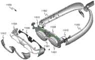
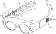
图1是示出根据本文描述的实施例的通过可穿戴增强现实(AR)装置观察的AR场景的图。FIG. 1 is a diagram illustrating an AR scene viewed by a wearable augmented reality (AR) device according to embodiments described herein.
图2A示出了立体三维(3D)显示。Figure 2A shows a stereoscopic three-dimensional (3D) display.
图2B示出了可变深度平面调节(accommodation)距离。Figure 2B shows a variable depth plane accommodation distance.
图3A示出了给定深度平面处的调节-辐辏(vergence)焦点。Figure 3A shows accommodation-vergence focus at a given depth plane.
图3B示出了相对于给定深度平面的调节-辐辏失配。Figure 3B shows accommodation-vergence mismatch with respect to a given depth plane.
图4示出了超出给定深度平面的两个对象之间的比较的调节-辐辏失配。Figure 4 shows a comparative accommodation-vergence mismatch between two subjects beyond a given depth plane.
图5示出了根据一些实施例的深度平面选择和对调节-辐辏失配的影响。Figure 5 illustrates depth plane selection and effect on accommodation-vergence mismatch, according to some embodiments.
图6A-B示出了根据一些实施例的在给定某些深度平面的两个对象之间的比较的调节-辐辏失配。6A-B illustrate a comparative accommodation-vergence mismatch between two subjects given certain depth planes, according to some embodiments.
图7A-B示出了根据一些实施例的通过波导投射到用户眼睛中的光的横截面视图。7A-B illustrate cross-sectional views of light projected through a waveguide into a user's eye, according to some embodiments.
图8示出了根据一些实施例的由波导中的衍射光学元件(DOE)投射到用户眼睛的光场。Figure 8 illustrates the light field projected to a user's eye by a diffractive optical element (DOE) in a waveguide, according to some embodiments.
图9示出了根据一些实施例的由波导中的多个DOE投射到用户眼睛的宽光场。9 illustrates a wide light field projected by multiple DOEs in a waveguide onto a user's eye, according to some embodiments.
图10示出了根据一些实施例的由波导内的DOE外耦合到用户眼睛的聚焦光图案。Figure 10 illustrates a focused light pattern out-coupled from a DOE within a waveguide to a user's eye in accordance with some embodiments.
图11示出了根据一些实施例的注入到用户眼睛的多个子瞳孔中的子束(beamlets)。Figure 11 illustrates beamlets injected into multiple sub-pupils of a user's eye, according to some embodiments.
图12示出了根据一些实施例将某些准直子束聚焦通过子瞳孔,如同聚合子束是较大直径的单束。Figure 12 illustrates focusing certain collimated beamlets through a subpupil, as if the aggregated beamlets were a single larger diameter beam, according to some embodiments.
图13示出了根据一些实施例的将光外耦合到用户的眼睛的波导的堆叠,同时还允许世界光通过该堆叠透射到用户的眼睛。13 shows a stack of waveguides that outcouple light to a user's eye while also allowing world light to transmit through the stack to the user's eye, according to some embodiments.
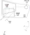
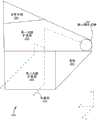
图14示出了根据一些实施例的内耦合DOE、正交DOE和出DOE,它们被配置为将注入的光重定向到多个波导中、穿过多个波导和从多个波导中导出。14 illustrates an in-coupling DOE, a quadrature DOE, and an out-DOE configured to redirect injected light into, through, and out of multiple waveguides, according to some embodiments.
图15示出了根据一些实施例的可穿戴增强现实显示系统。15 illustrates a wearable augmented reality display system according to some embodiments.
图16A示出了根据一些实施例的与真实世界环境交互的增强现实显示系统的用户的交互。16A illustrates user interaction of an augmented reality display system interacting with a real world environment in accordance with some embodiments.
图16B示出了根据一些实施例的观察光学器件组件的部件。Figure 16B illustrates components of a viewing optics assembly in accordance with some embodiments.
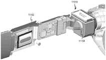
图17示出了根据一些实施例的具有某些部件的头戴式显示器的分解图。17 shows an exploded view of a head mounted display with certain components, according to some embodiments.
图18示出了根据一些实施例的观察光学器件组件的分解图。18 shows an exploded view of a viewing optics assembly in accordance with some embodiments.
图19示出了根据一些实施例的世界相机组件。Figure 19 illustrates a world camera assembly in accordance with some embodiments.
图20示意性地示出了根据本文描述的实施例的可用于向观察者呈现数字或虚拟图像的观察光学器件组件(VOA)中的光路。20 schematically illustrates optical paths in a viewing optics assembly (VOA) that may be used to present a digital or virtual image to a viewer, according to embodiments described herein.
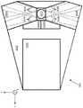
图21示出了根据本发明的实施例的目镜的示例。Figure 21 shows an example of an eyepiece according to an embodiment of the present invention.
图22示出了根据本发明的实施例的用于目镜的波导层的示例。Figure 22 shows an example of a waveguide layer for an eyepiece according to an embodiment of the invention.
图23示出了根据本发明的实施例的内耦合到目镜的波导中的光的单个子束的路径的示例。Figure 23 shows an example of the path of a single beamlet of light in-coupled into a waveguide of an eyepiece according to an embodiment of the present invention.
图24示出了根据本发明的实施例的用于波导的上/下拓扑的示例。Figure 24 shows an example of a top/bottom topology for a waveguide according to an embodiment of the present invention.
图25示出了根据本发明的实施例的用于波导的重叠拓扑的示例。Figure 25 shows an example of an overlapping topology for waveguides in accordance with an embodiment of the present invention.
图26示出了根据本发明的实施例的用于波导的成线(in-line)拓扑的示例。Figure 26 shows an example of an in-line topology for a waveguide according to an embodiment of the present invention.
图27示出了根据本发明的实施例的具有不同衍射效率区域的OPE的示例。Figure 27 shows an example of an OPE with regions of different diffraction efficiencies according to an embodiment of the present invention.
图28示出了根据本发明的实施例的用于波导的尖端和剪切拓扑的示例。Figure 28 shows an example of a tip and shear topology for a waveguide according to an embodiment of the present invention.
图29示出了根据本发明的实施例的用于波导的蝴蝶结拓扑的示例。Figure 29 shows an example of a bowtie topology for a waveguide according to an embodiment of the present invention.
图30A示出了根据本发明的实施例的用于波导的蝴蝶结拓扑的示例。Figure 30A shows an example of a bowtie topology for a waveguide according to an embodiment of the present invention.
图30B示出了根据本发明的实施例的用于波导的衍射光学特征的各种放大视图。30B shows various enlarged views of diffractive optical features for waveguides in accordance with embodiments of the present invention.
图30C示出了根据本发明的实施例的用于波导的OPE区域的光学操作。Figure 30C illustrates the optical operation of the OPE region for a waveguide in accordance with an embodiment of the present invention.
图31A示出了根据本发明的实施例的波导的示例,该波导包括具有两个叠加的衍射光栅的输入耦合器区域。Figure 31A shows an example of a waveguide including an input coupler region with two superimposed diffraction gratings in accordance with an embodiment of the present invention.
图31B示出了根据本发明的实施例的由两个叠加的衍射光栅构成的输入耦合器区域的示例的透视图。31B shows a perspective view of an example of an input coupler region composed of two superimposed diffraction gratings, according to an embodiment of the present invention.
图32A示出了根据本发明的实施例的具有紧凑形状因子的波导的示例。Figure 32A shows an example of a waveguide with a compact form factor in accordance with an embodiment of the present invention.
图32B示出了根据本发明的实施例的波导的输入耦合器区域的衍射光学特征的示例。32B shows an example of diffractive optical characteristics of the input coupler region of a waveguide according to an embodiment of the present invention.
图32C示出了根据本发明的实施例的波导的OPE区域的衍射光学特征的示例。32C shows an example of diffractive optical characteristics of the OPE region of a waveguide according to an embodiment of the present invention.
图33A示出了根据本发明的实施例的具有在单侧配置中的组合OPE/EPE区域的波导的示例。33A shows an example of a waveguide with combined OPE/EPE regions in a single-sided configuration, according to an embodiment of the present invention.
图33B示出了根据本发明的实施例的由SEM捕获的在单侧配置中的组合OPE/EPE区域的示例。33B shows an example of a combined OPE/EPE region in a single-sided configuration captured by SEM, according to an embodiment of the present invention.
图33C示出了根据本发明的实施例的波导内的光路的示例。Figure 33C shows an example of an optical path within a waveguide according to an embodiment of the present invention.
图33D示出了根据本发明的实施例的波导内的光路的示例的侧视图。33D shows a side view of an example of an optical path within a waveguide according to an embodiment of the present invention.
图34A示出了根据本发明的实施例的具有在双侧配置中的组合OPE/EPE区域的波导的示例。34A shows an example of a waveguide with combined OPE/EPE regions in a double-sided configuration, according to an embodiment of the present invention.
图34B示出了根据本发明的实施例的波导和光路的侧视图。Figure 34B shows a side view of a waveguide and optical path according to an embodiment of the present invention.
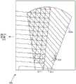
图35A-35J示出了根据本发明的实施例的用于在目镜中实施的波导的各种设计。35A-35J illustrate various designs of waveguides for implementation in eyepieces in accordance with embodiments of the present invention.
图36A是示出根据本发明的实施例的具有周期性变化的折射率的衍射元件的简化平面图。36A is a simplified plan view illustrating a diffractive element having a periodically varying refractive index according to an embodiment of the present invention.
图36B是示出根据本发明的实施例的具有折射率分布变化的衍射元件的简化平面图。36B is a simplified plan view illustrating a diffractive element with a change in refractive index distribution according to an embodiment of the present invention.
图36C是示出根据本发明的实施例的具有变化折射率的一组衍射元件的简化平面图。36C is a simplified plan view illustrating a set of diffractive elements with varying refractive indices in accordance with an embodiment of the present invention.
图36D是示出根据本发明的实施例的具有不同均匀折射率的一组衍射元件的简化平面图。36D is a simplified plan view illustrating a set of diffractive elements having different uniform indices of refraction in accordance with an embodiment of the present invention.
图36E是示出根据本发明的实施例的制造具有变化折射率的衍射元件的方法的简化流程图。36E is a simplified flow diagram illustrating a method of fabricating a diffractive element having a varying index of refraction in accordance with an embodiment of the present invention.
图36F是示出根据本发明的实施例的与平面基板邻接的变化折射率的膜的图像。36F is an image showing a variable index of refraction film adjoining a planar substrate in accordance with an embodiment of the present invention.
图36G是示出根据本发明的实施例的与衍射基板邻接的变化折射率的膜的图像。36G is an image showing a variable index of refraction film adjacent to a diffractive substrate in accordance with an embodiment of the present invention.
图36H是示出根据本发明的实施例的第一衍射元件中的变化折射率的膜的图像。Figure 36H is an image showing a variable refractive index film in a first diffractive element according to an embodiment of the present invention.
图36I是示出根据本发明的实施例的第二衍射元件中的变化折射率的膜的图像。Figure 36I is an image showing a variable refractive index film in a second diffractive element according to an embodiment of the present invention.
图36J是示出根据本发明的实施例的制造具有变化折射率的衍射元件的方法的简化流程图。36J is a simplified flow diagram illustrating a method of fabricating a diffractive element having a varying index of refraction in accordance with an embodiment of the present invention.
图36K是示出根据本发明的实施例的用于衍射元件的可变折射率结构的简化侧视图。36K is a simplified side view illustrating a variable index structure for a diffractive element according to an embodiment of the present invention.
图36L是示出根据本发明的实施例的用于衍射元件的多层可变折射率结构的简化侧视图。36L is a simplified side view illustrating a multilayer variable index structure for a diffractive element in accordance with an embodiment of the present invention.
图37是根据本发明的一些实施例的在基板上使用衍射结构的示例性光学系统的示意图。37 is a schematic diagram of an exemplary optical system using a diffractive structure on a substrate in accordance with some embodiments of the present invention.
图38示出了根据本发明的一些实施例的对于不同视场和不同厚度的波导呈现波干涉的电场强度的照片。38 shows photographs of electric field strengths exhibiting wave interference for different fields of view and waveguides of different thicknesses, in accordance with some embodiments of the present invention.
图39A是示出根据本发明的一些实施例的未抖动OPE及其输出图像的简化图。Figure 39A is a simplified diagram illustrating an undithered OPE and its output image according to some embodiments of the invention.
图39B是示出根据本发明的一些实施例的正弦抖动的OPE及其输出图像的简化图。Figure 39B is a simplified diagram showing an OPE of sinusoidal dither and its output image in accordance with some embodiments of the present invention.
图39C是示出根据本发明的一些实施例的优化的2D抖动OPE及其输出图像的简化图。Figure 39C is a simplified diagram illustrating an optimized 2D dithering OPE and its output image according to some embodiments of the present invention.
图39D示出了根据本发明的一些实施例的将具有许多伪像的图像与具有较少伪像的图像进行比较的照片。Figure 39D shows a photograph comparing an image with many artifacts to an image with fewer artifacts, according to some embodiments of the present invention.
图40A示出了根据本发明的一些实施例的将连续相位变化图案添加到衍射结构的示例。Figure 40A shows an example of adding a continuous phase change pattern to a diffractive structure in accordance with some embodiments of the present invention.
图40B示出了根据本发明的一些实施例的来自具有带有和不带有相位变化的衍射结构的光学系统的输出图像。Figure 40B shows output images from an optical system with diffractive structures with and without phase change, according to some embodiments of the present invention.
图40C示出了根据本发明的一些实施例的将离散相位变化图案添加到衍射结构的示例。Figure 40C shows an example of adding a discrete phase change pattern to a diffractive structure in accordance with some embodiments of the present invention.
图41A示出了说明根据本发明的一些实施例的用于光栅的不同缓慢变化的抖动图案的简化图。41A shows a simplified diagram illustrating different slowly varying dither patterns for gratings in accordance with some embodiments of the present invention.
图41B-C示出了根据本发明的一些实施例的可以在衍射结构中实施的不同类型的离散相位变化图案。41B-C illustrate different types of discrete phase change patterns that may be implemented in diffractive structures in accordance with some embodiments of the present invention.
图42A是示出根据本发明的一些实施例的用于光栅的附加抖动变化图案的简化图。42A is a simplified diagram illustrating additional dither variation patterns for gratings in accordance with some embodiments of the present invention.
图42B示出了根据本发明的一些实施例的制造具有变化的光栅高度的衍射光栅以在衍射光栅中实施相位扰动的示例方法。42B illustrates an example method of fabricating a diffraction grating with varying grating heights to implement phase perturbations in the diffraction grating in accordance with some embodiments of the present invention.
图42C是根据本发明的一些实施例的制造具有相位变化图案的衍射结构的示例性方法的流程图。42C is a flow diagram of an exemplary method of fabricating a diffractive structure with a phase change pattern in accordance with some embodiments of the present invention.
图42D是根据本发明的一些实施例的由抖动的目镜层操控光的示例性方法的流程图。42D is a flowchart of an exemplary method of manipulating light by a dithered eyepiece layer in accordance with some embodiments of the present invention.
图43是根据本发明的一些实施例的在包括波导中的衍射结构的示例装置中衍射的光的示意图。43 is a schematic diagram of light diffracted in an example device including diffractive structures in a waveguide, according to some embodiments of the present invention.
图44A是示出根据本发明的一些实施例的通过光束倍增器的光路的简化图。Figure 44A is a simplified diagram showing the optical path through a beam multiplier according to some embodiments of the present invention.
图44B是示出根据本发明的一些实施例的通过操控波干涉的束倍增器的光路的简化图。44B is a simplified diagram showing the optical path through a beam multiplier for steering wave interference, according to some embodiments of the present invention.
图45A-B是根据本发明的一些实施例的比较通过光栅结构的抖动的光路的简化图。45A-B are simplified diagrams comparing optical paths through dithering of a grating structure in accordance with some embodiments of the present invention.
图46是示出根据本发明的一些实施例的近眼显示装置中的观察光学器件系统的框图。46 is a block diagram illustrating a viewing optics system in a near-eye display device according to some embodiments of the present invention.
图47A是根据本发明的一些实施例的波导显示器的框图。Figure 47A is a block diagram of a waveguide display according to some embodiments of the invention.
图47B是根据本发明的一些实施例的使用波导显示器产生的输出图像。Figure 47B is an output image produced using a waveguide display according to some embodiments of the invention.
图48A是示出根据本发明的一些实施例的进入波导显示器的多个输入的框图。48A is a block diagram illustrating multiple inputs into a waveguide display according to some embodiments of the present invention.
图48B是根据本发明的一些实施例的来自具有多个输入的波导显示器的输出图像。Figure 48B is an output image from a waveguide display with multiple inputs, according to some embodiments of the present invention.
图48C是示出根据本发明的一些实施例的用于使用多个输入光束在波导显示器中生成多个非相干图像的方法的简化流程图。48C is a simplified flow diagram illustrating a method for generating multiple incoherent images in a waveguide display using multiple input beams in accordance with some embodiments of the present invention.
图49A是示出根据本发明的一些实施例的利用衍射分束器进入波导显示器的单个输入的框图。49A is a block diagram illustrating a single input into a waveguide display using a diffractive beamsplitter in accordance with some embodiments of the present invention.
图49B是示出根据本发明的一些实施例的用于使用衍射分束器在波导显示器中生成多个非相干图像的方法的简化流程图。49B is a simplified flow diagram illustrating a method for generating multiple incoherent images in a waveguide display using a diffractive beam splitter according to some embodiments of the present invention.
图50A是示出根据本发明的一些实施例的利用多个衍射分束器进入波导显示器的单个输入的框图。50A is a block diagram illustrating a single input into a waveguide display using multiple diffractive beamsplitters in accordance with some embodiments of the present invention.
图50B是示出根据本发明的一些实施例的用于使用多个衍射分束器在波导显示器中生成多个非相干图像的方法的简化流程图。50B is a simplified flowchart illustrating a method for generating multiple incoherent images in a waveguide display using multiple diffractive beamsplitters in accordance with some embodiments of the present invention.
图51A是示出根据本发明的一些实施例的远心投影仪系统的框图。51A is a block diagram illustrating a telecentric projector system according to some embodiments of the present invention.
图51B是示出根据本发明的一些实施例的非远心投影仪系统的框图。51B is a block diagram illustrating a non-telecentric projector system according to some embodiments of the present invention.
图52是示出根据本发明的一些实施例的用于抑制近眼显示装置中的远心投影仪的反射的系统的框图。52 is a block diagram illustrating a system for suppressing reflections from a telecentric projector in a near-eye display device, according to some embodiments of the present invention.
图53A是示出根据本发明的一些实施例的衍射光学元件上的正方形晶格光栅结构的框图。53A is a block diagram illustrating a square lattice grating structure on a diffractive optical element according to some embodiments of the present invention.
图53B是示出根据本发明的一些实施例的衍射光学元件上的圆形的圆元件光栅结构的照片。53B is a photograph showing a circular circular element grating structure on a diffractive optical element according to some embodiments of the present invention.
图54A是根据本发明的一些实施例的衍射光学元件的二元光栅脊的顶视图。54A is a top view of a binary grating ridge of a diffractive optical element according to some embodiments of the invention.
图54B是根据本发明的一些实施例的衍射光学元件的横切二元光栅脊的顶视图。Figure 54B is a top view across a binary grating ridge of a diffractive optical element according to some embodiments of the invention.
图55是根据本发明的一些实施例的衍射光学元件的横切偏置光栅脊的顶视图。55 is a top view of a diffractive optical element cross-sectioned with an offset grating ridge in accordance with some embodiments of the present invention.
图56是示出根据本发明的一些实施例的衍射光学元件上的三角形元件光栅结构的照片。56 is a photograph showing a triangular element grating structure on a diffractive optical element according to some embodiments of the present invention.
图57是示出根据本发明的一些实施例的衍射光学元件上的椭圆形元件光栅结构的照片。57 is a photograph showing an elliptical element grating structure on a diffractive optical element according to some embodiments of the present invention.
图58是示出根据本发明的一些实施例的抑制近眼显示装置中的远心投影仪的反射的方法的简化流程图。58 is a simplified flowchart illustrating a method of suppressing reflections from a telecentric projector in a near-eye display device, according to some embodiments of the present invention.
图59A是示出根据本发明的一些实施例的以恒定的衍射效率为特征的衍射结构的平面图的简化示意图。59A is a simplified schematic diagram illustrating a plan view of a diffractive structure characterized by constant diffractive efficiency, according to some embodiments of the present invention.
图59B是示出根据本发明的一些实施例的以具有不同衍射效率的区域为特征的衍射结构的平面图的简化示意图。59B is a simplified schematic diagram illustrating a plan view of a diffractive structure featuring regions with different diffractive efficiencies, according to some embodiments of the present invention.
图59C是示出根据本发明的一些实施例的衍射结构的平面图的简化示意图,该衍射结构以具有不同衍射效率的区域为特征。Figure 59C is a simplified schematic diagram showing a plan view of a diffractive structure featuring regions with different diffraction efficiencies in accordance with some embodiments of the present invention.
图60A-H是示出根据本发明的一些实施例的用于使用灰阶光刻来制造可变衍射效率光栅的过程的简化过程流程图。60A-H are simplified process flow diagrams illustrating a process for fabricating variable diffraction efficiency gratings using grayscale lithography in accordance with some embodiments of the present invention.
图61A-C是示出根据本发明的一些实施例的用于制造具有不同表面高度的区域的过程的简化过程流程图。61A-C are simplified process flow diagrams illustrating a process for fabricating regions with different surface heights in accordance with some embodiments of the present invention.
图62A-C是示出根据本发明的一些实施例的用于制造具有不同衍射效率的光栅的区域的过程的简化过程流程图。62A-C are simplified process flow diagrams illustrating a process for fabricating regions of a grating having different diffraction efficiencies, according to some embodiments of the present invention.
图63A-H是示出根据本发明的一些实施例的使用多级蚀刻过程来制造以不同衍射效率为特征的区域的简化过程流程图。63A-H are simplified process flow diagrams illustrating the use of a multi-stage etching process to fabricate regions characterized by different diffraction efficiencies in accordance with some embodiments of the present invention.
图64A-H是示出根据本发明的一些实施例的使用多级蚀刻过程来制造可变衍射效率光栅的简化过程流程图。64A-H are simplified process flow diagrams illustrating the use of a multi-stage etching process to fabricate a variable diffraction efficiency grating in accordance with some embodiments of the present invention.
图65是根据本发明的一些实施例的内耦合光栅的简化横截面视图。65 is a simplified cross-sectional view of an incoupling grating in accordance with some embodiments of the present invention.
图66是示出根据本发明的一些实施例的制造具有变化的衍射效率的衍射结构的方法的简化流程图。66 is a simplified flow diagram illustrating a method of fabricating a diffractive structure with varying diffractive efficiencies in accordance with some embodiments of the present invention.
图67是示出根据本发明的一些实施例的制造以具有不同衍射效率的区域为特征的衍射结构的方法的简化流程图。67 is a simplified flow diagram illustrating a method of fabricating a diffractive structure featuring regions with different diffractive efficiencies in accordance with some embodiments of the present invention.
图68A-D是示出根据本发明的一些实施例的用于使用灰阶光刻来制造可变衍射效率光栅的过程的简化过程流程图。68A-D are simplified process flow diagrams illustrating a process for fabricating variable diffraction efficiency gratings using grayscale lithography in accordance with some embodiments of the present invention.
图69是示出根据本发明的一些实施例的制造具有变化的衍射效率的衍射结构的方法的简化流程图。69 is a simplified flow diagram illustrating a method of fabricating a diffractive structure with varying diffractive efficiencies in accordance with some embodiments of the present invention.
图70示意性地示出了根据一些实施例的目镜的局部横截面视图。70 schematically illustrates a partial cross-sectional view of an eyepiece in accordance with some embodiments.
图71示意性地示出了根据一些实施例的一些波长选择反射器的示例性反射光谱。Figure 71 schematically illustrates exemplary reflection spectra of some wavelength selective reflectors in accordance with some embodiments.
图72示意性地示出了根据一些其它实施例的目镜的局部横截面视图。Figure 72 schematically illustrates a partial cross-sectional view of an eyepiece according to some other embodiments.
图73示意性地示出了根据一些其它实施例的目镜的局部横截面视图。73 schematically illustrates a partial cross-sectional view of an eyepiece according to some other embodiments.
图74示意性地示出了根据一些实施例的长通滤波器和短通滤波器的示例性反射光谱。Figure 74 schematically illustrates exemplary reflectance spectra of long pass filters and short pass filters in accordance with some embodiments.
图75示出了根据一些实施例的超表面的示例。Figure 75 shows an example of a metasurface according to some embodiments.
图76示出了根据一些实施例的用于具有图75中所示的一般结构的超表面的透射和反射光谱的绘图。76 shows plots of transmission and reflection spectra for a metasurface having the general structure shown in FIG. 75, according to some embodiments.
图77A和图77B分别示出了根据一些实施例的由一维纳米束形成的超表面的顶视图和侧视图。77A and 77B illustrate top and side views, respectively, of a metasurface formed from one-dimensional nanobeams, according to some embodiments.
图77C和图77D分别示出了根据一些其它实施例的由一维纳米束形成的超表面的平面图和侧视图。Figures 77C and 77D show plan and side views, respectively, of a metasurface formed from one-dimensional nanobeams, according to some other embodiments.
图78A和图78B分别示出了根据一些实施例的由在基板的表面上形成的多个纳米天线形成的单层二维超表面的顶视图和侧视图。78A and 78B illustrate top and side views, respectively, of a monolayer two-dimensional metasurface formed from multiple nanoantennas formed on the surface of a substrate, according to some embodiments.
图78C和图78D分别示出了根据一些实施例的多层二维超表面的平面图和侧视图。78C and 78D illustrate plan and side views, respectively, of a multilayer two-dimensional metasurface in accordance with some embodiments.
图79示出了根据一些实施例的针对TE偏振、图77C和图77D中所示的超表面的、针对对应于绿色(实线)的波长以及对应于红色(虚线)的波长的、根据入射角的模拟反射率的绘图。Figure 79 shows the metasurfaces shown in Figures 77C and 77D for wavelengths corresponding to green (solid lines) and wavelengths corresponding to red (dotted lines) as a function of incidence for TE polarization, according to some embodiments A plot of the simulated reflectivity of the corners.
图80示出了根据一些实施例的针对TE偏振的、图77C和图77D中所示的超表面的模拟反射光谱(实线)和模拟透射光谱(虚线)的绘图。80 shows plots of simulated reflection spectra (solid lines) and simulated transmission spectra (dashed lines) of the metasurface shown in FIGS. 77C and 77D for TE polarization, according to some embodiments.
图81示出了根据一些实施例的针对TM偏振、图77C和图77D中所示的超表面的、针对对应于绿色(实线)的波长以及对应于红色(虚线)的波长的入射角的函数的模拟反射率的绘图。FIG. 81 shows for TM polarization, for the metasurfaces shown in FIGS. 77C and 77D, for angles of incidence corresponding to wavelengths corresponding to green (solid lines) and wavelengths corresponding to red (dashed lines), according to some embodiments A plot of the simulated reflectance of the function.
图82示出了根据一些实施例的针对TM偏振的、图77C和图77D中所示的超表面的模拟反射光谱(实线)和模拟透射光谱(虚线)的绘图。82 shows plots of simulated reflection spectra (solid lines) and simulated transmission spectra (dashed lines) of the metasurface shown in FIGS. 77C and 77D for TM polarization, according to some embodiments.
图83A-83F示意性地示出了根据一些实施例的如何通过交错的两个子超表面来形成复合超表面。83A-83F schematically illustrate how a composite metasurface is formed by interleaving two sub-metasurfaces, according to some embodiments.
图84A和图84B分别示出了根据一些实施例的超表面的顶视图和侧视图。Figures 84A and 84B show top and side views, respectively, of a metasurface in accordance with some embodiments.
图84C示意性地示出了根据一些实施例的图84A和图84B中所示的超表面的作为入射角函数的反射光谱。Figure 84C schematically illustrates reflectance spectra as a function of angle of incidence for the metasurfaces shown in Figures 84A and 84B, according to some embodiments.
图85A示意性地示出了根据一些实施例的目镜8500的局部侧视图。Figure 85A schematically illustrates a partial side view of an
图85B示意性地示出了根据一些实施例的图85A中所示的波长选择反射器的顶视图。Figure 85B schematically illustrates a top view of the wavelength selective reflector shown in Figure 85A, according to some embodiments.
图86A示意性地示出了根据一些实施例的体积相位全息图的局部横截面视图。86A schematically illustrates a partial cross-sectional view of a volume phase hologram in accordance with some embodiments.
图86B示意性地示出了根据一些实施例的图86A中所示的体积相位全息图的反射光谱。Figure 86B schematically illustrates the reflectance spectrum of the volume phase hologram shown in Figure 86A, according to some embodiments.
图86C示意性地示出了根据一些实施例的体积相位全息图的局部横截面视图。86C schematically illustrates a partial cross-sectional view of a volume phase hologram in accordance with some embodiments.
图86D示意性地示出了根据一些实施例的图86C中所示的体积相位全息图的反射光谱。Figure 86D schematically illustrates the reflectance spectrum of the volume phase hologram shown in Figure 86C, according to some embodiments.
图86E示意性地示出了根据一些实施例的复合体积相位全息图的局部横截面视图。86E schematically illustrates a partial cross-sectional view of a composite volume phase hologram in accordance with some embodiments.
图86F示意性地示出了根据一些实施例的在波导上形成的复合体积相位全息图的侧视图。86F schematically illustrates a side view of a composite volume phase hologram formed on a waveguide in accordance with some embodiments.
图87是示出根据一个实施例的投影仪的示例的示意图。FIG. 87 is a schematic diagram illustrating an example of a projector according to one embodiment.
图88是示出根据一个实施例的投影仪的示例的示意图。88 is a schematic diagram illustrating an example of a projector according to one embodiment.
图89是示出根据一个实施例的使用设置在每个波导中的内耦合光栅将多种颜色的光耦合到对应的波导中的示意图。89 is a schematic diagram illustrating the use of incoupling gratings disposed in each waveguide to couple multiple colors of light into corresponding waveguides, according to one embodiment.
图90A-90C是根据一个实施例的分布式子光瞳架构的顶视图。90A-90C are top views of a distributed sub-pupil architecture according to one embodiment.
图91是示出根据一个实施例的用于多个深度平面的颜色的时序编码的示意图。91 is a schematic diagram illustrating temporal encoding of color for multiple depth planes, according to one embodiment.
图92A是示出根据一个实施例的投影仪组件的示意图。92A is a schematic diagram illustrating a projector assembly according to one embodiment.
图92B是示出图92A中所示的投影仪组件的展开示意图。Figure 92B is an expanded schematic view showing the projector assembly shown in Figure 92A.
图93A是示出根据一个实施例的投影仪组件中的伪像形成的示意图。93A is a schematic diagram illustrating artifact formation in a projector assembly according to one embodiment.
图93B是示出图93A中所示的投影仪组件中的伪像形成的展开示意图。Figure 93B is an expanded schematic view illustrating artifact formation in the projector assembly shown in Figure 93A.
图94示出了图92A中所示的投影仪组件的场景中的伪像的存在。Figure 94 illustrates the presence of artifacts in the scene of the projector assembly shown in Figure 92A.
图95A是示出根据一个实施例的具有伪像防止的投影仪组件的示意图。95A is a schematic diagram illustrating a projector assembly with artifact prevention, according to one embodiment.
图95B是示出根据一个实施例的减少光学伪像的方法的流程图。95B is a flowchart illustrating a method of reducing optical artifacts, according to one embodiment.
图96示出了使用图95A中所示的投影仪组件的伪像强度的减少。Figure 96 shows the reduction in artifact intensity using the projector assembly shown in Figure 95A.
图97A是示出根据一个实施例的由投影显示系统中的内耦合光栅元件的反射产生的伪像形成的示意图。Figure 97A is a schematic diagram illustrating artifact formation resulting from reflection of in-coupling grating elements in a projection display system, according to one embodiment.
图97B是示出由图97A中所示的投影显示系统中的内耦合光栅的反射产生的伪像形成的展开示意图。Figure 97B is an expanded schematic diagram illustrating artifact formation resulting from reflection of the incoupling grating in the projection display system shown in Figure 97A.
图98是示出根据一个实施例的来自内耦合光栅元件的反射的示意图。Figure 98 is a schematic diagram illustrating reflections from incoupling grating elements, according to one embodiment.
图99A是示出根据另一实施例的具有伪像防止的投影仪组件的示意图。99A is a schematic diagram illustrating a projector assembly with artifact prevention according to another embodiment.
图99B是示出根据实施例的减少光学系统中的伪像的方法的流程图。99B is a flowchart illustrating a method of reducing artifacts in an optical system according to an embodiment.
图100示出了在没有反射防止元件的情况下在目镜处的光反射。Figure 100 shows light reflection at the eyepiece without a reflection preventing element.
图101A示出了根据一个实施例的使用伪像防止元件对反射的阻挡。FIG. 101A illustrates blocking of reflections using an artifact prevention element, according to one embodiment.
图101B是示出根据一个实施例的减少光学系统中的伪像的方法的流程图。101B is a flowchart illustrating a method of reducing artifacts in an optical system, according to one embodiment.
图102示出了根据一个实施例的使用替代几何伪像防止元件对反射的阻挡。Figure 102 illustrates the use of alternative geometric artifact prevention elements to block reflections according to one embodiment.
图103是根据一个实施例的具有多个伪像防止元件的投影仪组件的示意图。103 is a schematic diagram of a projector assembly having multiple artifact preventing elements, according to one embodiment.
图104A是示出根据一个实施例的使用滤色器的具有伪像防止的投影仪组件的示意图。104A is a schematic diagram illustrating a projector assembly with artifact prevention using color filters, according to one embodiment.
图104B是示出图104A中所示的投影仪组件的展开示意图。Figure 104B is an expanded schematic view showing the projector assembly shown in Figure 104A.
图104C是根据一个实施例的针对青色和品红色滤色器的透射绘图。Figure 104C is a transmission plot for cyan and magenta color filters, according to one embodiment.
图104D是示出根据一个实施例的滤色器和子光瞳的空间布置的示意图。Figure 104D is a schematic diagram illustrating the spatial arrangement of color filters and sub-pupils according to one embodiment.
图104E是示出根据一个实施例的减少光学系统中的伪像的方法的流程图。Figure 104E is a flowchart illustrating a method of reducing artifacts in an optical system according to one embodiment.
图105是示出根据一个实施例的滤色器系统的示意图。Figure 105 is a schematic diagram illustrating a color filter system according to one embodiment.
图106是示出根据一个实施例的线焊LED的示意图。106 is a schematic diagram illustrating a wire-bonded LED according to one embodiment.
图107是示出根据一个实施例的倒装芯片接合LED的示意图。107 is a schematic diagram illustrating a flip-chip bonded LED according to one embodiment.
图108是示出根据一个实施例的集成有抛物面扩束器的LED的示意图。108 is a schematic diagram illustrating an LED integrated with a parabolic beam expander, according to one embodiment.
图109是示出根据一个实施例的包括投影仪组件和目镜的单光瞳系统的示意图。109 is a schematic diagram illustrating a single pupil system including a projector assembly and an eyepiece, according to one embodiment.
图110A-110B示出了光学装置的透视图;110A-110B show perspective views of an optical device;
图110C示出了具有附接到其上的多个电子部件的光学装置的光学器件框架的透视图;110C shows a perspective view of an optics frame of an optical device with a plurality of electronic components attached thereto;
图110D示出了光学装置的前带和传感器盖的透视图;Figure 110D shows a perspective view of the front strap and sensor cover of the optical device;
图110E示出了光学器件框架和其它相关联部件的分解透视图;Figure 110E shows an exploded perspective view of the optics frame and other associated components;
图111A-111D示出了热如何沿光学装置的各种部件分布;Figures 111A-111D illustrate how heat is distributed along various components of an optical device;
图111E-111G示出了利用与前述实施例中所示的被动对流相反的强制对流的散热系统的透视图和侧横截面视图;111E-111G show perspective and side cross-sectional views of a heat dissipation system utilizing forced convection as opposed to passive convection shown in the previous embodiments;
图112A示出了描绘热通过传导层从PCB到热扩散层的传送的横截面视图;112A shows a cross-sectional view depicting the transfer of heat from the PCB to the thermal diffusion layer through the conductive layer;
图112B示出了列出传导层的材料性质的图表;Figure 112B shows a graph listing the material properties of the conductive layer;
图113A-113D示出了覆盖在光学装置的部件上的各种热图;Figures 113A-113D show various thermal maps overlaid on components of an optical device;
图114A示出了仅一个臂能够相对于框架移动的光学装置的透视图;Figure 114A shows a perspective view of an optical device with only one arm movable relative to the frame;
图114B示出了说明光学装置的哪些部分相对于彼此变形最大的覆盖物;Figure 114B shows a covering illustrating which parts of the optical device are most deformed relative to each other;
图114C示出了示出柔性臂的运动范围的光学装置的顶视图;以及Figure 114C shows a top view of the optical device showing the range of motion of the flexible arm; and
图114D示出了说明其中两个臂弯曲的光学装置的部分如何相对于彼此移动的覆盖物。Figure 114D shows a cover illustrating how the parts of the optical device where the two arms are bent move relative to each other.
图115是示出根据本发明的一些实施例的用于观察光学器件组件的目镜的优化的简化图。115 is a simplified diagram illustrating optimization of an eyepiece for viewing optics assemblies, according to some embodiments of the present invention.
图116A是示出根据本发明的一些实施例的对于EPE中的圆形顶部的总厚度变化(TTV)对场畸变的影响的曲线图。116A is a graph showing the effect of total thickness variation (TTV) on field distortion for a circular top in an EPE, according to some embodiments of the present invention.
图116B是示出根据本发明的一些实施例的对于平坦基板的TTV对场畸变的影响的曲线图。Figure 116B is a graph showing the effect of TTV on field distortion for a flat substrate in accordance with some embodiments of the invention.
图116C是示出根据本发明的一些实施例的测量的TTV的曲线图。Figure 116C is a graph showing measured TTV according to some embodiments of the present invention.
图117A是示出根据本发明的一些实施例的用于闪耀光栅结构的制造过程的简化图。117A is a simplified diagram illustrating a fabrication process for a blazed grating structure in accordance with some embodiments of the present invention.
图117B示出说明根据本发明的一些实施例的闪耀光栅结构的照片。117B shows a photograph illustrating a blazed grating structure according to some embodiments of the present invention.
图117C是根据本发明的一些实施例的将三角形光栅结构的制造过程与闪耀光栅结构进行比较的简化图。117C is a simplified diagram comparing the fabrication process of a triangular grating structure to a blazed grating structure, according to some embodiments of the present invention.
图117D是示出与根据本发明的一些实施例的平顶ICG结构与点顶ICG结构相比较的简化图。Figure 117D is a simplified diagram showing a comparison of a flat-topped ICG structure to a point-topped ICG structure in accordance with some embodiments of the present invention.
图118是示出根据本发明的一些实施例的闪耀光栅结构的制造过程的简化过程流程图。118 is a simplified process flow diagram illustrating a fabrication process for a blazed grating structure in accordance with some embodiments of the present invention.
图119A示出了说明根据本发明的一些实施例的闪耀几何形状看起来如何一次湿法蚀刻的照片。Figure 119A shows a photograph illustrating how a blaze geometry looks like a wet etch in accordance with some embodiments of the present invention.
图119B示出了说明根据本发明的一些实施例的四种不同临界尺寸(CD)的示例性扫描电子显微镜(SEM)图像的照片。Figure 119B shows photographs illustrating exemplary scanning electron microscope (SEM) images of four different critical dimensions (CDs) in accordance with some embodiments of the present invention.
图119C示出了根据本发明的一些实施例的产生高效IC的二氧化硅中的输入耦合器(IC)的CD的控制。119C illustrates control of the CD of an input coupler (IC) in silicon dioxide producing a high efficiency IC according to some embodiments of the present invention.
图120是示出根据本发明的一些实施例的基于压印的制造的简化图。Figure 120 is a simplified diagram illustrating imprint-based manufacturing in accordance with some embodiments of the present invention.
图121A是示出根据本发明的一些实施例的用于波导的图案化光栅结构的制造过程的简化过程流程图。121A is a simplified process flow diagram illustrating a fabrication process for a patterned grating structure for a waveguide in accordance with some embodiments of the present invention.
图121B是示出根据本发明的一些实施例的使用PVD型过程沉积的ZrOx膜的折射率的曲线图。121B is a graph showing the refractive index of ZrOx films deposited using a PVD-type process according to some embodiments of the present invention.
图121C是示出根据本发明的一些实施例的基于沉积参数和蚀刻轮廓沉积的材料的变化轮廓的简化图。Figure 121C is a simplified diagram showing the changing profile of the deposited material based on deposition parameters and etch profile in accordance with some embodiments of the present invention.
图121D示出了根据本发明的一些实施例的在基板上的大区域上图案化的高折射率线的照片。Figure 121D shows a photograph of high index lines patterned over a large area on a substrate in accordance with some embodiments of the present invention.
图122示出了根据本发明一些实施例的多级二元光栅的照片。Figure 122 shows a photograph of a multilevel binary grating according to some embodiments of the invention.
图123是示出根据本发明的一些实施例的使用停止层堆叠的多级二元光栅结构的制造过程的简化过程流程图。123 is a simplified process flow diagram illustrating a fabrication process for a multi-level binary grating structure using stop layer stacking in accordance with some embodiments of the present invention.
图124是示出根据本发明的一些实施例的使用蚀刻掩模的多级二元光栅结构的制造过程的简化过程流程图。124 is a simplified process flow diagram illustrating a fabrication process for a multi-level binary grating structure using an etch mask in accordance with some embodiments of the present invention.
图125示出了说明根据本发明的一些实施例的由于蚀刻掩模的不同沉积角度而导致的不同光栅结构的简化过程流程图。125 shows a simplified process flow diagram illustrating different grating structures due to different deposition angles of the etch mask in accordance with some embodiments of the present invention.
图126A是示出根据本发明的一些实施例的恒定光栅结构的简化平面图。126A is a simplified plan view illustrating a constant grating structure according to some embodiments of the present invention.
图126B是示出根据本发明的一些实施例的通过恒定光栅结构的光强度的曲线图。126B is a graph showing light intensity through a constant grating structure according to some embodiments of the invention.
图127A是示出根据本发明的一些实施例的具有渐变占空比的光栅结构的简化平面图。127A is a simplified plan view illustrating a grating structure with a graded duty cycle in accordance with some embodiments of the present invention.
图127B是示出根据一些实施例的通过具有渐变占空比的光栅结构的光强度的曲线图。127B is a graph showing light intensity through a grating structure with a graded duty cycle, according to some embodiments.
图127C是示出根据本发明的一些实施例的具有渐变占空比的光栅结构的放大简化图。127C is an enlarged simplified diagram illustrating a grating structure with a graded duty cycle in accordance with some embodiments of the present invention.
图128是根据本发明的一些实施例的通过具有渐变占空比的光栅结构的目镜层操控光的示例性方法的流程图。128 is a flowchart of an exemplary method of manipulating light through an eyepiece layer having a grating structure with graded duty cycle, according to some embodiments of the present invention.
具体实施方式Detailed ways
图1是示出根据本文描述的实施例的通过可穿戴增强现实(AR)装置观察的AR场景的图。参考图1,描绘了增强现实场景100,其中AR技术的用户看到以人、树、背景中的建筑物和混凝土平台120为特征的真实世界公园式设置106。除了这些项目之外,AR技术的用户还感知到他“看到”站在真实世界平台(120)上的机器人雕像(110),以及飞过的卡通式头像角色(102),其看起来是大黄蜂的拟人化,即使这些元素(102,110)在真实世界中不存在。由于人类视觉感知和神经系统的极端复杂性,产生促进虚拟图像元素在其它虚拟或真实世界图像元素中的舒适、感觉自然的、丰富的呈现的VR或AR技术是有挑战性的。FIG. 1 is a diagram illustrating an AR scene viewed by a wearable augmented reality (AR) device according to embodiments described herein. Referring to FIG. 1 , an
图2A示出了用于向用户呈现3D图像的传统显示系统。向用户显示两个不同的图像5和7,每只眼睛4和6一个图像。图像5和7沿平行于观察者视线的光学或z轴与眼睛4和6隔开距离10。图像5和7是平的,并且眼睛4和6可以通过呈现单个调节状态、触发辐辏反射以匹配该调节状态而聚焦在图像上。这种系统依赖于人类视觉系统来组合图像5和7以提供组合图像的深度感知。Figure 2A shows a conventional display system for presenting 3D images to a user. The user is shown two
然而,应当理解,人类视觉系统更复杂并且提供真实的深度感知更具挑战性。例如,图2A中描绘的传统3D显示系统的许多观察者发现这种系统是不舒服的或者根本不会感知到深度感,这是由于调节和辐辏的失配,即,在特定深度平面上观察对象的视线可能不是聚焦在同一深度平面的最优调节距离。如图2B中所示,可以在可变的或多个深度平面12处显示内容的系统可以提供更类似于眼睛的自然功能的调节-辐辏状态。However, it should be appreciated that the human visual system is more complex and more challenging to provide true depth perception. For example, many observers of the conventional 3D display system depicted in Figure 2A find such systems uncomfortable or not perceiving depth at all due to a mismatch in accommodation and vergence, ie, viewing at a particular depth plane The subject's line of sight may not be the optimal accommodation distance to focus on the same depth plane. As shown in Figure 2B, a system that can display content at variable or
例如,图3A描绘了在深度平面14处观察内容15的眼睛4和6。如图所示,内容15位于深度平面14处,其中深度平面14可以是具有单个深度平面的给定3D系统(诸如立体系统)的深度平面。调节距离Ad(即,眼睛4和6聚焦的距离)与辐辏距离Vd(即眼睛4和6观察的距离)相同。然而,在图3B中,内容15y旨在比深度平面14更远地被感知,例如立体3D系统被配置用于两米处的深度平面但是内容旨在显现为距用户3m。如图所示,眼睛4和6中的每一个将具有聚焦在深度平面14上的调节距离Ad,但是眼睛4和6中的每一个将在深度平面14上具有相应的辐辏点15a和15b,以及整体辐辏距离Vd1。Vd1与Ad的比率可以被称为“调节-辐辏失配”(AVM),并且在某些AVM处,用户可能不再感知到内容15y的深度或者可能感到不适,因为视觉和神经系统试图校正该大的AVM。For example, FIG. 3A depicts
然后,应当理解,传统的3D立体显示器不利于调节-辐辏反射并且引起调节-辐辏失配。在调节和辐辏之间提供更好匹配的显示系统可以形成更逼真和舒适的3D影像模拟。Then, it should be understood that conventional 3D stereoscopic displays are detrimental to accommodation-verb reflections and cause accommodation-verb mismatches. A display system that provides a better match between adjustment and vergence can result in a more realistic and comfortable 3D image simulation.
图4示出了使用多个深度平面模拟三维影像的益处。参考图4,内容15y和15z被放置在距眼睛4和6的相应辐辏距离Vd2和Vd3处,但是系统仅具有一个深度平面14以产生调节距离Ad2。眼睛4和6呈现特定的调节状态以使15y和15z沿z轴聚焦。因此,为了聚焦于15y,眼睛4和6呈现在深度平面14上的15c和15d的辐辏位置;为了聚焦于15z,眼睛4和6呈现在深度平面14上的15e和15f的辐辏位置。很明显,与观察15y的辐辏姿态15c和15d相比,眼睛4和6具有观察15z的更宽的辐辏姿态15e和15f,并且对于深度平面14,如果15e和15f在深度平面14上并置,则将感觉到自然观察。辐辏姿态中的该差异以及Vd3与Ad2和Vd2与Ad2的比率都是AVM的说明。Figure 4 illustrates the benefits of using multiple depth planes to simulate 3D imagery. Referring to Figure 4,
为了创建尽可能自然的3D体验,一些实施例实施多个深度平面以将AVM限制在给定阈值以下并且减少否则可能由AVM导致的用户不适。例如,图5描绘了容许的AVM被配置为0.333屈光度的实施例。该屈光度距离对应于距用户三米,其中对于在该深度平面处渲染的内容,AVM将为零。由于屈光度与距离是反比关系,随着内容接近光学无穷远,AVM将逐渐接近但绝不会超过0.333屈光度。当内容渲染为比3m更接近用户时,可以实施第二深度平面,使得内容可以在第二深度平面处显示而不会上升到0.333屈光度AVM以上。然后内容将在AVM方面增加,因为它甚至更接近该第二深度平面,就像对象非常接近眼睛自然发生一样。例如,当手指从手臂的长度朝向眼睛时,眼睛将越来越难以保持眼睛上的相同聚焦质量,手指可能显现为在主导和非主导眼睛的焦点或用户的视场之间跳跃或者可能完全分成两个图像。本领域技术人员将理解,附加的AVM阈值是可能的并且将引起在对应于该AVM阈值的不同距离处的深度平面放置,或者在特定AVM阈值内渲染甚至更接近眼睛的内容的甚至更多的深度平面是可能的。图5仅示出了具有0.333和1屈光度的深度平面(分别为3米和1米)以将所有渲染的内容维持在低于0.333屈光度的AVM阈值的七十六厘米之外的一个实施例。In order to create the most natural 3D experience possible, some embodiments implement multiple depth planes to limit the AVM below a given threshold and reduce user discomfort that might otherwise be caused by the AVM. For example, Figure 5 depicts an embodiment where the allowable AVM is configured to be 0.333 diopters. This diopter distance corresponds to three meters from the user, where the AVM will be zero for content rendered at this depth plane. Since diopter is inversely proportional to distance, as the content approaches optical infinity, the AVM will gradually approach but never exceed 0.333 diopters. When the content is rendered closer to the user than 3m, a second depth plane can be implemented so that the content can be displayed at the second depth plane without rising above the 0.333 diopter AVM. Then the content will increase in terms of AVM as it is even closer to this second depth plane, as happens naturally when the object is very close to the eye. For example, as the finger goes from the length of the arm towards the eye, it will become increasingly difficult for the eye to maintain the same quality of focus on the eye, the finger may appear to jump between the focal points of the dominant and non-dominant eyes or the user's field of view or may split entirely two images. Those skilled in the art will understand that additional AVM thresholds are possible and will result in depth plane placement at different distances corresponding to that AVM threshold, or even more rendering of content even closer to the eye within a particular AVM threshold Depth planes are possible. Figure 5 shows only one embodiment with depth planes of 0.333 and 1 diopter (3 meters and 1 meter, respectively) to maintain all rendered content beyond seventy-six centimeters below the AVM threshold of 0.333 diopter.
图6B描绘了多个深度平面的益处。图6A是图4的副本,为了便于与图6B进行比较而重新显示。在图6B中,在距眼睛4和6的调节距离Ad3处添加第二深度平面16。为了聚焦于内容15z,眼睛4和6不再需要呈现如图6A中的15e和15f的辐辏姿态。但是,可以替代地呈现辐辏姿态15g和15h。与图6A的Vd3与Ad2相比较具有低的Vd3与Ad3比率,用户可以在深度平面16处聚焦于更远的内容15z,具有与在深度平面14处聚焦于更近内容15y所需的几乎相同的视觉感知。换句话说,借助于图6B的多深度平面系统,为了观察相同的内容15z,15g和15h的辐辏位置比辐辏位置15e和15f小得多并且更自然。Figure 6B depicts the benefit of multiple depth planes. Figure 6A is a duplicate of Figure 4, redisplayed for ease of comparison with Figure 6B. In Figure 6B, a
图7A描绘了向人眼呈现外部光图案的简化的显示配置,该外部光图案可以被舒适地感知为对物理现实的增强,具有高水平的图像质量和3D感知,并且能够让让真实世界的光和图像被感知。如图所示,单个至少部分透明的波导104接收光图案106,并且波导104内的衍射光栅102将光外耦合到眼睛58。在一些实施例中,衍射光栅102被配置用于特定深度平面,使得当晶状体45通过调节-辐辏反射聚焦于其接收的光图案时,视网膜54将光图案处理为位于配置的深度平面处的图像。在一些实施例中,光图案106被配置用于特定深度平面,使得当晶状体45通过调节-辐辏反射聚焦于其接收的光图案上时,视网膜54将光图案处理为位于配置的深度平面处的图像。Figure 7A depicts a simplified display configuration presenting to the human eye an external light pattern that can be comfortably perceived as an enhancement of physical reality, has a high level of image quality and 3D perception, and enables real-world Light and images are perceived. As shown, a single at least partially
如图所示,仅出于说明性目的,光图案106是进入波导104的基于光子的辐射图案,但是本领域技术人员将理解,光图案106可以容易地是注入波导104中的单个光束,并且在外耦合到眼睛58之前,通过全内反射传播到衍射光栅102。本领域技术人员将进一步理解,可以采用多个衍射光栅102以期望的方式将光图案106引导到眼睛58。As shown, the
为了针对这种系统创建更丰富的视场,图7B描绘了第二至少部分透明的波导204,其被配置为以与图6A中所示的非常相同的方式将光图案206外耦合到眼睛58。第二波导204通过衍射光栅202将光图案206外耦合到眼睛58。眼睛58在视网膜54上接收光图案206,但是晶状体45通过与光图案106所需的不同的调节-辐辏反射来感知不同深度平面处的光206。例如,光图案106以第一深度感知500聚集在视网膜54的一部分中,而光图案206以第二深度感知502聚集在视网膜54的第二部分中。在光图案106和206对应于相同渲染的增强现实内容的情况下,与在图6A中描绘的通过单个深度平面简单产生的图像相比,深度丰富度创建更逼真且更舒适的感知图像。此外,在一些实施例中,光图案106和206的帧序列配置可以以高频率向眼睛58呈现帧序列,其与在单个深度平面处由视网膜54感知的窄投影相比,提供横跨多个深度和更全的视场的单个相干增强现实场景或运动中的增强现实内容的感知。To create a richer field of view for such a system, Figure 7B depicts a second at least partially
图8进一步描绘了平面波导216的简化版本,该平面波导216可以包括至少两个波导,该至少两个波导被配置为传播特定波长的光,但是在相对于眼睛58不同的深度平面处传播。如图所示,可以是衍射光学元件(DOE)的衍射光栅220已嵌入平面波导216的整个垂直长度内,使得随着光图案沿平面波导216全内反射,它在多个位置处与DOE 220相交。随着光外耦合到眼睛58,尽管如此,由于平面波导216内的DOE 220的衍射效率,一部分仍然可以继续传播。随着该部分继续全内反射通过平面波导216,它们可能遇到附加的DOE 220光栅并且外耦合到眼睛,或者其它部分可以沿平面波导216的长度通过全内反射继续传播。FIG. 8 further depicts a simplified version of the
优选地,DOE 220具有相对低的衍射效率,使得仅在平面波导216内传播的光图案的一部分在DOE 220的任何给定相交点处朝向眼睛58衍射,而剩余部分继续经由全内反射移动通过平面波导216。因此,携带任何图像信息的光图案被分成多个相关光束,该多个相关光束在多个位置处离开平面波导216,并且结果是入射到眼睛58上的外耦合光的大图案,以从单个光图案产生丰富的图像感知。Preferably,
图9描绘了多个外耦合的光图案,示出了当光在朝向眼睛58的z方向中外耦合之前在x和y方向二者中传播波导时入射在眼睛58上的甚至更丰富的光场。具有被配置为允许在z方向中外耦合的光图案的部分衍射并允许其它部分在z方向中的外耦合之前在x或y方向中全内反射的一系列DOE 220的实施例产生横跨眼睛58的整个视网膜的影像。FIG. 9 depicts a number of out-coupled light patterns showing an even richer light field incident on the
图10描绘了来自波导106的外耦合的DOE 110的多个外耦合光图案的视网膜图案;如图所示,图10示出了可由单个光图案106激活的多个视网膜区域,使得光图案的更宽视场或时间顺序成帧能够激发视网膜的不同部分以感知所渲染的增强现实内容的运动。本领域技术人员将理解,当与图9中描绘的丰富视场图案组合时,借助于整个波导106中的DOE110,视网膜可以接收大量的光图案。如所描绘的,图10示出了聚焦在眼睛58的晶状体45中的所有光。图11示出了“子瞳孔”系统,其中多个入射光图案子束332在离散的垂直焦点处通过眼睛58的单独的小出射瞳孔330进入眼睛。通过这样做,光图案的较小子束可被聚集以被感知为较大直径的光束,光图案的较小子束可以更容易地投影和衍射通过波导或者可以携带诸如波长的特定光图案性质。例如,尽管图7A的光图案从光图案106产生晶状体45中的焦点;子束332可以非常小并且通过产生多个子瞳孔330仍然产生相同的效应。10 depicts retinal patterns of multiple out-coupled light patterns from an out-coupled
换句话说,可以使用一组多个窄光束来模拟采用较大直径的可变焦点光束进行的操作;如果子束直径保持在约0.5mm的最大值,它们保持相对静态的聚焦水平,并且在需要时产生离焦的感知,可以选择子束角度轨迹以产生就像更大的离焦光束的效应(这种散焦处理可能与对于更大的光束的高斯模糊处理不同,但是将产生多模态点扩散函数,该多模态点扩散函数可以以与高斯模糊类似的方式解释)。In other words, a set of multiple narrow beams can be used to simulate operation with larger diameter variable focus beams; if the beamlet diameter is kept at a maximum of about 0.5mm, they maintain a relatively static level of focus and To create the perception of out-of-focus when needed, the beamlet angle trajectories can be chosen to produce an effect like a larger out-of-focus beam (this defocusing may not be the same as Gaussian blurring for larger beams, but will produce multimode modal point spread function, this multimodal point spread function can be interpreted in a similar way to Gaussian blur).
在一些实施例中,子束未被机械偏转以形成该聚集的焦点效应,而是眼睛接收许多子束的超集,该子束的超集包括多个入射角和子束与光瞳相交的多个位置;为了表示来自特定观察距离的给定像素,来自超集的包括适当的入射角和与光瞳的相交点(如同它们是从空间中的相同共享原点发射的)的子束的子集通过颜色和强度来匹配以表示聚合波前,而超集中的与共享原点不一致的子束与该颜色和强度没有匹配且不会被感知。In some embodiments, beamlets are not mechanically deflected to form the focused focal effect, but rather the eye receives a superset of many beamlets, the superset of beamlets comprising multiple angles of incidence and multiple intersections of beamlets and pupils positions; to represent a given pixel from a particular viewing distance, a subset of beamlets from the superset including the appropriate angle of incidence and intersection with the pupil (as if they were emitted from the same shared origin in space) Matched by color and intensity to represent the aggregated wavefront, sub-beams in the superset that are not aligned with the shared origin do not match that color and intensity and will not be perceived.
图12示出了表示眼睛58的视场中的聚合准直光束334的子束的另一子集。这里,眼睛58被调节到无穷远以考虑准直光束334,因此准直光束334内的子束落在视网膜的同一点上,并且由该子束产生的像素被感知为合焦。类似地,准直光束326落在视网膜的不同部分上以感知视场的该区域中的像素。相反,如果选择作为光线的发散扇到达眼睛的子束的不同子集,则这些子束将不会落在视网膜的相同位置,并且不被感知为合焦,直到眼睛将调节移动到与该光线扇的几何原点相匹配的近点为止。FIG. 12 shows another subset of beamlets representing aggregated collimated
图13描绘了平面波导的堆叠664,每个平面波导通过内耦合DOE 690馈送光图案,该内耦合DOE 690将特定波长的光衍射到堆叠644的平面波导中。每个波导包括多个DOE680、682、684、686和688,其被配置为将光衍射通过相应的平面波导并朝向眼睛58外耦合,以横跨视场或在多个深度平面处产生增强现实内容的感知。图13描绘了仅用于说明目的的堆叠644内的五个波导,优选地,堆叠664包括六个波导,对应于与红色、绿色和蓝色波长的光中的每一个处的深度平面相关联的两个波导。世界光144也可以透过并透射通过堆叠644,因为堆叠644内的每个波导至少部分透明,以允许结合对真实世界环境的自然感知来渲染增强现实内容。13 depicts a stack 664 of planar waveguides each feeding a light pattern through an in-
在一些实施例中,并且如图14中所示,到增强现实显示系统的目镜1200可包括设置在波导上的多个DOE类型,以将具有特定性质的光引导到用户的眼睛。多个光图案1240、1242和1244被注入到包括波导1210、1220和1230的波导堆叠中。在一些实施例中,多个光图案1240、1242和1244从共同光源注入,但表示共同光源内的不同波长。在一些实施例中,光图案1240、1242和1244中的每一个是特定波长的单独光束,例如红色、绿色和蓝色光。在一些实施例中,通过内耦合DOE 1212、1222和1232将光图案1240、1242和1244中的每一个光图案注入到相应的波导1210、1220和1230。每个内耦合DOE 1212、1222和1232将光图案1240、1242或1244的特定波长的至少一部分光衍射到波导1210、1220或1230中的一个波导内,该波导1210、1220或1230被配置为传播内耦合DOE 1212、1222和1232的相同波长的内耦合光。在一些实施例中,在内耦合之后,光图案1240、1242和1244分别传播到OPE 1214、1224和1234中。OPE 1214、1224和1234分别将一部分光衍射到EPE 1250、1252和1254中,其中光图案1240、1242和1244在z方向中朝向用户的眼睛外耦合。In some embodiments, and as shown in FIG. 14, an
在一些实施例中,通过一系列波导和多个DOE衍射并且然后外耦合到用户的眼睛的多个光图案的净效应(net effect)产生由用户舒适地感知的虚拟或增强现实内容的视场渲染和深度平面放置。In some embodiments, the net effect of multiple light patterns diffracted by a series of waveguides and multiple DOEs and then out-coupled to the user's eye produces a field of view of virtual or augmented reality content that is comfortably perceived by the user Rendering and depth plane placement.
图15示出了可穿戴显示系统80的示例。显示系统80包括头戴式显示器62,以及支持该显示器62的功能的各种机械和电子模块和系统。显示器62可以耦合到框架64,该框架64可由显示系统用户或观察者60佩戴并被配置为将头戴式显示器62定位在用户60的眼睛前方。在一些实施例中,扬声器66耦合到框架64并定位在用户耳道附近(在一些实施例中,未示出的另一个扬声器定位在用户的另一个耳道附近,以提供立体声/可成形声音控制)。头戴式显示器62诸如通过有线引线或无线连接可操作地耦合68到本地数据处理模块70,该本地数据处理模块70可以以各种配置安装,诸如固定地附接到框架64,固定地附接到由用户佩戴的头盔或帽子,嵌入耳机中,或以其它方式可移除地附接到用户60(例如,以背包式配置,以带耦合方式配置)。FIG. 15 shows an example of a
本地数据处理模块70可以包括处理器以及数字存储器,诸如非易失性存储器(例如闪存),两者都可以用于辅助数据的处理、高速缓存和存储。数据包括如下数据:a)从传感器(其可以例如可操作地耦合到框架64)捕获的数据或以其它方式附接到用户60,诸如图像捕获装置(诸如相机)、麦克风、惯性测量单元、加速度计、指南针、GPS单元、无线装置和/或陀螺仪;和/或b)使用远程处理模块72和/或远程数据存储库74获取和/或处理的数据,可能在这种处理或取得之后通过显示器62。本地数据处理模块70可以由通信链路76、78(诸如经由有线或无线通信链路)可操作地耦合到远程处理模块72和远程数据存储库74,使得这些远程模块72、74可操作地耦合到彼此并且可用作本地处理和数据模块70的资源。The local
在一些实施例中,本地数据处理模块70可以包括被配置为分析和处理数据和/或图像信息的一个或多个处理器。在一些实施例中,远程数据存储库74可以包括数字数据存储设备,该数字数据存储设备可以通过因特网或“云”资源配置中的其它网络配置获得。在一些实施例中,所有数据被存储在本地处理和数据模块中并且在本地处理和数据模块中执行所有计算,允许从远程模块完全自主使用。In some embodiments, local
在一些实施例中,本地数据处理模块70可操作地耦合到电池82。在一些实施例中,电池82是诸如优于柜台电池的可移除电源。在其它实施例中,电池82是锂离子电池。在一些实施例中,电池82包括在可穿戴显示系统80的非操作时间期间由用户60可充电的内部锂离子电池和可移除电池,使得用户可以在更长时间段内操作可穿戴显示系统80而无需系在电源上为锂离子电池充电或无需关闭可穿戴显示系统来更换电池。In some embodiments, local
图16A描绘了用户1660佩戴着随着用户1660移动通过真实世界环境1600渲染增强现实内容的增强现实显示系统。用户将增强现实显示系统定位在位置1610处,并且增强现实显示系统记录相对于位置1610的可通过世界的环境信息,诸如与映射特征或方向音频输入的姿势关系。位置1610被聚合到数据输入1612并且至少由诸如在图15中描绘的远程处理模块72中的可通过世界模块1620处理。如从输入1612确定的,可通过世界模块1620确定在何处以及如何可将增强现实内容1630放置在真实世界中,诸如放置在固定元素1632(如图16A所示的桌子)上或在尚未在视场1640内或相对于真实世界1642的映射网格模型的结构内。如所描绘的,固定元素1632用作真实世界内的可以存储在可通过世界模块1620中的任何固定元素的代理,使得用户1660可以感知桌子1632上的内容,而不必在每次用户1660看到它时都映射桌子1632。因此,固定内容1632可以是来自先前建模会话的映射网格模型,或者从单独的用户确定,但是仍然存储在可通过世界模块1620上以供将来由多个用户参考。因此,可通过世界模型可以从先前映射的环境识别环境1600并且在没有用户的装置首先映射环境1600的情况下显示增强现实内容,从而节省计算过程和周期并且避免任何渲染的增强现实内容的延迟。16A depicts a
类似地,真实世界1642的映射网格模型可以由增强现实显示系统创建,并且用于交互和显示增强现实内容1630的适当表面和度量可以被映射并存储在可通过世界模块1620中以供用户或其他用户将来取得,而无需重新映射或建模。在一些实施例中,聚合的数据输入1612是诸如地理定位、用户标识和当前活动的输入,以向可通过世界模块1620指示哪些固定元素1632可用、哪个增强现实内容1630最后被放置在固定元素1632上,以及是否显示该相同的内容(这种增强现实内容是“持久的”内容,而不管用户观察特定的可通过世界模型)。Similarly, a mapped mesh model of the
图16B描绘了观察光学器件组件1664和伴随部件的示意图。在一些实施例中,面向用户眼睛1666,两个眼睛跟踪相机1662检测用户眼睛1666的度量,诸如眼睛形状、眼睑遮挡、瞳孔方向和用户眼睛1666上的闪烁。在一些实施例中,深度传感器1690(诸如飞行时间传感器)向世界发射中继信号以确定到给定对象的距离。在一些实施例中,世界相机1650记录大于周边的视图以映射真实世界环境并检测可能影响增强现实内容的输入。相机1680可以进一步捕获用户视场内的真实世界图像的特定时间戳。世界相机1650、相机1680和深度传感器1690中的每一个具有1652、1682和1692的相应视场,以从真实世界场景(诸如图16A中所示的真实世界环境1600)收集数据并记录真实世界场景。Figure 16B depicts a schematic view of the
惯性测量单元1670可以确定观察光学器件组件1664的移动和取向。在一些实施例中,每个部件可操作地耦合到至少一个其它部件;例如,深度传感器1690可操作地耦合到眼睛跟踪相机1662,作为对测量的调节相对用户眼睛1666正在观察的实际距离的确认。
图17描绘了头戴式显示器1700,诸如图15中描绘的头戴式显示器62。观察光学器件组件1702包括刚性框架1708,投影仪1704耦合到该刚性框架1708。在一些实施例中,投影仪1704包括具有LED照射器和空间光调制器的LCOS机构。在一些实施例中,观察光学器件组件1702进一步包括目镜1706。在一些实施例中,目镜1706包括多个波导,该多个波导被配置为将来自投影仪1704的光引导到头戴式显示器1700的用户的眼睛。在一些实施例中,观察光学器件组件1702进一步包括眼睛跟踪相机(未示出),该眼睛跟踪相机被配置为收集头戴式显示器1700的佩戴者的眼睛跟踪数据,诸如眼睑位置或瞳孔方向。FIG. 17 depicts a head mounted
在一些实施例中,观察光学器件组件1702容纳布置在刚性框架1708上的附加传感器和部件,诸如主控制板(PCB)1716。PCB 1716容纳各种处理器和电路以操作组装在观察光学器件组件1702和刚性框架1708内的各种部件。在一些实施例中,世界相机1718在观察光学器件组件1702的任一端附接到刚性框架1708。在一些实施例中,世界相机1718替代地设置在观察光学器件组件1702的目镜1706之间。在一些实施例中,深度传感器1719附接到目镜1706之间的刚性框架1708。在一些实施例中,深度传感器1719是垂直腔表面发射激光器(VCSEL),在一些实施例中,深度传感器1719是边缘发射激光器或其它飞行时间传感器。本领域技术人员将理解,可以容纳在观察光学器件组件1702内并且由主控制板1716可操作地控制的其它传感器和部件,例如IMU或图片相机可以设置在观察光学器件组件1702上或附接到刚性框架1708。In some embodiments,
在一些实施例中,前带1710耦合到观察光学器件组件1702。前带1710既保护观察光学器件组件1702的部件免受外部元件的影响,又用作头戴式显示器1700的用户与观察光学器件之间的热屏障。在一些实施例中,传感器盖1712附接到前带1710以进一步保护观察光学器件组件1702及其上的部件。In some embodiments,
在一些实施例中,臂1714耦合到刚性框架1708并且被配置为横穿头戴式显示系统1700的用户的头部并且将目镜1706保持在用户眼睛的前方。在一些实施例中,臂1714被配置为搁置在用户的耳朵上;在一些实施例中,框架臂1714被配置为保持向内张力以抓住用户的头部以保持在用户头部上的固定位置。在一些实施例中,垫1715附接到臂1714的内侧(内侧是臂1714的与用户接触的一侧)。在一些实施例中,垫1715包括散热器以减轻头戴式显示器1700内的热效应。在一些实施例中,垫1715由软泡沫制成或涂覆有橡胶界面,以当从臂1714的向内张力压缩抵靠用户的头部上时产生半变形,并且仍然为用户产生舒适的感觉。In some embodiments,
在一些实施例中,音频组件1720耦合到刚性框架1708并横穿臂1714中的任一个臂以将扬声器1722放置在头戴式显示系统1700的用户的耳朵附近。在一些实施例中,PCB1716进一步控制到音频组件1720的音频输入和输出。在一些实施例中,音频组件1720包括麦克风,该麦克风记录来自外部世界的声音并将它们中继到主控制板1716。给定这种音频输入的主控制板1716可以执行各种功能。例如,给定来自音频组件1720的麦克风输入,头戴式显示器1700可以存储它们以供将来取得(诸如在图15中描绘的远程数据存储库74中),响应于给定的音频输入改变增强现实内容性能(例如,口头“关闭”命令可以关闭整个系统),或者将音频输入发送给通信装置的其他用户(例如,电话呼叫、用于电子传递的语音消息传递)。电缆1724便于整个头戴式显示器1700的部件之间的通信,以及到本地数据处理模块(诸如图15中描绘的本地数据处理模块70)的通信。In some embodiments,
在一些实施例中,内盖1707可以向用户提供进一步的光学效应。例如,内盖1707可以包括处方透镜,以将增强现实内容的光学性质调节到用户的特定视觉处方。这种处方透镜将设置在用户的眼睛和头戴式显示器1700的目镜1706之间。在一些实施例中,内盖1707可包括可拆卸的光修改器,诸如偏振透镜,以反射或吸收某些光。In some embodiments, the
图18描绘了观察光学器件组件1800的分解视图。刚性框架1808容纳目镜1806,该目镜1806可包括多个波导,用于将光内耦合到头戴式显示器1700(图17中所示)的用户的眼睛中,观察光学器件组件1800是该头戴式显示器1700的一部分。在横截面视图中以1804'描绘为具有偏振分束器和多个透镜的LCOS系统的投影仪1804在内耦合点1805处光学耦合到目镜1806。在一些实施例中,内耦合点1805是用于将光注入到目镜1806和目镜1806内的波导的入口点。FIG. 18 depicts an exploded view of
目镜1806固定到刚性框架1808。刚性框架1808进一步容纳安装结构1811。安装结构1811可以容纳设置在观察光学器件组件1800的世界侧上的盖透镜1809,或观察光学器件组件的用户侧上的图17中所示的内盖1707。在一些实施例中,盖透镜1809可包括抗划伤材料或其它保护性覆盖物,以防止目镜1806与诸如来自指尖的油或来自外部环境的灰尘和碎屑接触。在一些实施例中,盖透镜1809可以包括光修改器,诸如偏振透镜,以反射或吸收某些光。在一些实施例中,除了多个波导之外,目镜1806还包括这种保护性盖透镜。在一些实施例中,眼睛跟踪系统1803耦合到安装结构1811,以将一对眼睛跟踪相机设置在安装结构1811的底部,向上看向用户的眼睛。
图19进一步更详细地描绘了可以附接到头戴式显示系统的观察光学器件组件或刚性框架的各种传感器和部件。深度传感器1903被示出为完全组装为可以附接到观察光学器件组件或刚性框架的深度传感器。深度传感器1903可以进一步由深度传感器壳体组件1905、垂直腔表面发射激光器(VCSEL)1902和深度成像器1904组成。19 further depicts in greater detail the various sensors and components that may be attached to the viewing optics assembly or rigid frame of the head mounted display system.
六自由度(6DoF)传感器1906容纳在6DoF壳体1907内,并通过6DoF折曲物1909可操作地耦合到观察光学器件组件(或如图17所示的主控制板1716)。6DoF传感器1906可向头戴式显示器提供惯性测量单元信息,以向头戴式显示器提供关于用户的位置、姿势和运动的信息。在一些实施例中,惯性测量由耦合到世界相机组件1918的IMU 1926提供。IMU 1926通过加速度计和陀螺仪测量提供位置信息,并且在一些实施例中可操作地耦合到6DoF传感器1909以启动对观察光学组件内的传感器或部件位置的改变。例如,指示用户正在旋转头部姿势以向下看的IMU 1926的测量可以促使6DoF传感器1906重定向深度传感器1902以及时或甚至在IMU 1926测量之前也向下调节深度测量,以避免测量上的延迟。换句话说,如果IMU 1926正在检测运动,则6DoF传感器1906被配置为操控观察光学器件组件内的任何一个或多个传感器和部件,以继续渲染与检测到的运动匹配的准确内容,而没有可由用户检测的增强现实内容中的延迟。观察光学器件显示器可以主控一个或多个6DoF传感器1906或IMU 1926。A six degrees of freedom (6DoF)
图19进一步描绘了世界相机组件1918。在一些实施例中,世界相机组件1918包括四个世界相机,两个设置为相对于用户的视场基本上向外看,并且两个设置为基本上倾斜地看以向观察光学器件组件提供大于外围的视场信息。当然可以使用附加的或更少的世界相机。图片相机1928可以耦合到世界相机组件1918以捕获用户或图片相机1928的视场内的实时图像或视频。世界相机组件1918可以向测量的传感器信息提供视觉信息,或激活某些传感器。例如,世界相机可以对传感器提供约束以仅检测和收集世界相机的视场内的信息,或者可以与投影仪通信以仅使用处理器功率来渲染视场内的内容。例如,如果世界相机将某些对象带入某些视场,则如图15中所示的本地数据处理模块70内的图形处理器单元(GPU)可以仅被激活以渲染增强现实内容;而头戴式显示器或可穿戴显示系统内的深度传感器和加速度计以及地理定位器可以记录相对于渲染增强现实内容的环境输入,GPU可以不被激活,直到世界相机实际将这种输入带入用户的视场中为止。FIG. 19 further depicts the
例如,世界相机组件1918的大于外围的视场可以开始在GPU中处理增强现实内容的成像,即使内容尚未在用户的视场内。在其它实施例中,大于外围的视场可以捕获来自真实世界的数据和图像,并且在世界相机组件1918的视场内但是在用户的视场之外向用户的活动视场显示提示。For example, a larger than peripheral field of view of the
图20示意性地示出了根据一个实施例的可用于向观察者呈现数字或虚拟图像的观察光学器件组件(VOA)中的光路。VOA包括可由观察者佩戴的投影仪2001和目镜2000。在一些实施例中,投影仪2001可包括一组红色LED、一组绿色LED和一组蓝色LED。例如,投影仪2001可以包括两个红色LED、两个绿色LED和两个蓝色LED。目镜2000可包括一个或多个目镜层。在一个实施例中,目镜2000包括三个目镜层,一个目镜层用于三原色(红色、绿色和蓝色)中的每一个。在另一实施例中,目镜2000可包括六个目镜层,一组目镜层用于三原色中的每一个,被配置用于在一个深度平面处形成虚拟图像,并且另一组目镜层用于三原色中的每一个,被配置用于在另一个深度平面处形成虚拟图像。在又一实施例中,目镜2000可以包括用于三原色中的每一个的三个或更多个目镜层,用于三个或更多个不同的深度平面。每个目镜层包括平面波导,并且可以包括内耦合光栅(ICG)2007、正交光瞳扩展器(OPE)区域2008和出射光瞳扩展器(EPE)区域2009。Figure 20 schematically illustrates optical paths in a viewing optics assembly (VOA) that may be used to present a digital or virtual image to a viewer, according to one embodiment. The VOA includes a projector 2001 and an eyepiece 2000 that can be worn by an observer. In some embodiments, projector 2001 may include a set of red LEDs, a set of green LEDs, and a set of blue LEDs. For example, projector 2001 may include two red LEDs, two green LEDs, and two blue LEDs. Eyepiece 2000 may include one or more eyepiece layers. In one embodiment, eyepiece 2000 includes three eyepiece layers, one for each of the three primary colors (red, green, and blue). In another embodiment, eyepiece 2000 may include six eyepiece layers, one set of eyepiece layers for each of the three primary colors configured to form a virtual image at one depth plane, and another set of eyepiece layers for the three primary colors Each is configured to form a virtual image at another depth plane. In yet another embodiment, eyepiece 2000 may include three or more eyepiece layers for each of the three primary colors, for three or more different depth planes. Each eyepiece layer includes a planar waveguide and may include an incoupling grating (ICG) 2007 , an orthogonal pupil expander (OPE) region 2008 and an exit pupil expander (EPE) region 2009 .
投影仪2001将图像光投影到目镜层2000中的ICG 2007上。ICG 2007将来自投影仪2001的图像光耦合到平面波导中,在朝向OPE区域2008的方向中传播。波导在水平方向中通过全内反射(TIR)传播图像光。OPE区域2008还包括衍射元件,该衍射元件使来自ICG 207的图像光倍增(multiply)并将来自ICG 207的图像光重定向为在波导中朝向EPE区域2009传播。换句话说,OPE区域2009在正交方向中使传递到EPE的不同部分的子束倍增。EPE区域2009包括衍射元件,该衍射元件将在波导中传播的图像光的一部分在大致垂直于目镜层2000的平面的方向中朝向观察者的眼睛2002外耦合并引导。以该方式,由投影仪2001投影的图像可以由观察者的眼睛2002观察。The projector 2001 projects the image light onto the ICG 2007 in the eyepiece layer 2000 . The ICG 2007 couples the image light from the projector 2001 into the planar waveguide, propagating in the direction towards the OPE region 2008 . The waveguide propagates the image light by total internal reflection (TIR) in the horizontal direction. The OPE region 2008 also includes diffractive elements that multiply the image light from the ICG 207 and redirect the image light from the ICG 207 to propagate in the waveguide towards the EPE region 2009 . In other words, the OPE region 2009 multiplies the beamlets delivered to different parts of the EPE in orthogonal directions. The EPE region 2009 includes diffractive elements that outcouple and direct a portion of the image light propagating in the waveguide towards the observer's
如上所述,由投影仪2001生成的图像光可以包括三原色中的光,即蓝色(B)、绿色(G)和红色(R)。这种图像光可以被分离成组成颜色,使得每种组成颜色的图像光可以耦合到目镜中的相应波导。本公开的实施例不限于所示投影仪的使用,并且可以在本公开的各种实施例中利用其它类型的投影仪。As described above, the image light generated by the projector 2001 may include light of three primary colors, ie, blue (B), green (G), and red (R). This image light can be separated into component colors so that each component color of image light can be coupled to a corresponding waveguide in the eyepiece. Embodiments of the present disclosure are not limited to the use of the projector shown, and other types of projectors may be utilized in various embodiments of the present disclosure.
尽管投影仪2001包括LED光源2003和硅基液晶(LCOS)空间光调制器(SLM)2004,但是本公开的实施例不限于该投影仪技术并且可以包括其它投影仪技术,包括光纤扫描投影仪、可变形镜装置、微机械扫描仪、激光光源而不是LED的使用、光学器件的其它布置、波导和包括前照灯设计的分束器等。Although the projector 2001 includes an LED light source 2003 and a liquid crystal on silicon (LCOS) spatial light modulator (SLM) 2004, embodiments of the present disclosure are not limited to this projector technology and may include other projector technologies including fiber scanning projectors, Deformable mirror devices, micromachined scanners, use of laser light sources instead of LEDs, other arrangements of optics, waveguides and beam splitters including headlamp designs, etc.
图21示出了根据本发明的实施例的目镜2100的示例。目镜2100可以包括世界侧盖窗2102和眼侧盖窗2106,以保护定位于世界侧盖窗2102和眼侧盖窗2106之间的一个或多个波导2104。在一些实施例中,目镜2100不包括世界侧盖窗2102和眼侧盖窗2106中的一者或二者。一个或多个波导2104可以以分层布置耦合在一起,使得每个单独波导耦合到其相邻波导中的一者或二者。在一些实施例中,该一个或多个波导2104经由边缘密封(诸如图22中所示的边缘密封2208)耦合在一起,使得一个或多个波导2104彼此不直接接触。Figure 21 shows an example of an
图22示出了根据本发明的实施例的用于目镜2200的波导层2204的示例。如可以看出的,每个波导2204可以在彼此顶部上对准,具有空气空间或设置在其间的另一种材料。在一个说明性示例中,世界侧盖窗2202和眼侧盖窗2206可以是0.330mm厚。在这种示例中,每个波导2204可以是0.325mm厚。另外,每层之间可以是0.027mm厚的空气空间。普通技术人员将认识到这些尺寸可以是不同的。图22还示出了每个波导2204可以与颜色和深度平面相关联。例如,目镜2200可以包括用于3米和1米深度平面的红色波导。红色波导可以在指定的深度处中继红光并将红光外耦合到用户的眼睛。目镜可以进一步包括用于3米和1米深度平面的蓝色波导。蓝色波导可以在指定的深度处中继蓝光并将蓝光外耦合到用户的眼睛。目镜可以进一步包括用于3米和1米深度平面的绿色波导。绿色波导可以在指定的深度处中继绿光并将绿光外耦合到用户的眼睛。普通技术人员将认识到,波导可以具有与图22中所示不同的顺序。深度平面涉及相应波导的光学功率,使得从该波导的EPE外耦合的光将发散并且被用户感知为源自距用户一定距离:本领域技术人员将可以理解,可以使用替代的指定深度,并且本文使用的和图22中的3米和1米深度平面仅用于说明目的。FIG. 22 shows an example of a
图23示出了根据本发明的实施例的耦合到目镜2300的波导2312中的光的单个子束的路径的示例。波导2312可以包括ICG 2320、OPE 2330和EPE 2340,每个设置在基板2302上或基板2302内,该基板2302由能够通过全内反射引导光波的材料(通常是具有高介电常数的介电材料)组成。在一些实施例中,目镜2300可包括三个波导2312、2314和2316,每个波导对应于特定波长的光。附加或更少的波导是可能的。与波导2312类似,波导2314和2316中的每一个波导可以包括ICG、OPE和EPE。在一些实施例中,注入光2322可以在与图23的描绘正交的z方向中在ICG 2320处进入目镜2300。注入光2322可以进入ICG 2320,其中ICG 2320内的光栅可以衍射入射光2322内的某些波长的光,并且内耦合光2322的其它波长继续通过目镜2310的后续波导层。在一些实施例中,ICG 2320是特定于特定波长的多个单独光栅。23 shows an example of the path of a single beamlet of light coupled into the
内耦合光2322可以由ICG 2320在波导内的某些方向中衍射,跨越诸如由在大致+x方向中朝向OPE 2330的扇形图案2324描绘的范围,但是也在跨越大致-x方向中远离OPE2330的扇形图案2326的范围内。跨越其它扇形图案的其它光路当然是可能的并且取决于投影光学器件,以及由ICG 2320配置的特定光栅和衍射图案。也就是说,光不作为发散光束衍射到波导中,但是在一些实施例中图像光的部分的渐进分布的采样可以产生跨目镜的逐渐扩展的子束分布图案。在所描绘的扇形图案2324内衍射的内耦合光2322通常可以沿光路2328进入OPE 2330并在+x方向中横穿,随着它撞击构成OPE 2330的衍射光栅,通过OPE2330进行伴随分布式采样,其中,该部分周期性地向下引导到EPE 2340并在朝向用户眼睛的-z方向中外耦合之前在-y方向中横穿。The in-coupled light 2322 may be diffracted by the
如图23所描绘的,与波导2312对应的波长中的许多光可能损失,这是由于方向损失(诸如衍射到扇形图案2326的光)导致;或由于捕获损失导致,该捕获损失由于不充分定位或设定尺寸的OPE 2330来捕获扇形图案2324内的所有光而导致。As depicted in Figure 23, much of the light in the wavelengths corresponding to the
图24示出了根据本发明的实施例的用于波导2400的上/下拓扑的示例。在一些实施例中,光可以与投影图像相关联或者来自投影图像。在一些实施例中,目镜和波导(例如波导2400)可以是至少部分透明的,使得用户可以透过目镜看到。在一些实施例中,波导2400可包括一个或多个区域,每个区域具有特定光栅。例如,波导2400可以包括具有内耦合DOE(例如ICG 2420)的输入区域。如在整个说明书中所描述的,内耦合DOE可以接收来自投影仪中继器的光。光可以进入与波导2400正交的输入区域。ICG 2420可以将光内耦合到波导2400中(即,进入基板2402)。Figure 24 shows an example of a top/bottom topology for a
在一些实施例中,波导2400可进一步包括第一区域,也称为具有第一光栅的波导的一部分(例如正交光瞳扩展器2430)。第一光栅可以设置在波导2400的平面表面内或平面表面上,以在通过ICG 2420衍射或内耦合到平面波导之后操控通过全内反射在波导2400中传播的光。在一些实施例中,第一光栅的周期性结构在整个第一区域中重定向图像光。随着内耦合的光束穿过第一光栅的周期性结构,这种重定向通过内耦合光束的衍射采样而发生。因此,本文描述的光栅可以通过多次衍射包括投影仪光瞳的光束来倍增(或克隆)投影图像的观察光瞳,以产生通过波导传播的多个子束。在许多情况下,每个子束携带图像数据,并且当多个子束最终如下所述从波导2400外耦合时,用户眼睛将出现的多个子束感知为传送图像信息的放大的采样光瞳。在一些实施例中,第一光栅可以将至少一部分光(例如克隆或采样的子束)引导到第二区域(例如EPE 2440)。第二区域或部分可以具有包括周期性结构的第二光栅。在这种实施例中,第一光栅的周期性结构的取向可以使得当子束与其一部分相互作用时采样的子束以标称的直角衍射,同时将子束朝向EPE衍射并进一步横跨OPE引导样本,以继续衍射和采样,并因此在OPE内复制图像光并将附加的子束朝向EPE2440衍射。尽管在一些实施例中光栅被讨论为示例性衍射光学结构,但是应当理解,本发明不限于衍射光栅,并且其它衍射结构(例如以六边形网格布置的多个岛)可以包括在本发明的范围内。In some embodiments, the
因此,应当理解,根据一些实施例,光的任何一部分可以由第一光栅横跨第一区域(例如OPE 2430)多次衍射,例如,并且如下面关于图30C更详细解释的,第一光栅内的周期性结构可以在给定方向中(例如朝向EPE 2440)衍射图像光的一部分,同时在第二方向中传输剩余部分。通过逐渐衍射光,可以将光视为横跨OPE 2430的“阶梯步进(stairstepping)”克隆的子束(即,通过衍射倍增或采样图像光的一部分)。例如,每当光线在大致x方向中行进时被衍射,光的一些部分可以朝向EPE 2440衍射。衍射光的一部分在大致x方向中继续通过OPE 2430,直到它再次在大致y-方向中将一部分朝向EPE 2440衍射,并且剩余部分在大致x方向中继续。在一些实施例中,光的中心光线可以由ICG 2420内耦合到波导中并且朝向OPE 2430引导。当在OPE 2430中行进时,中心光线可以由OPE 2430以直角衍射并且朝向EPE 2440引导(或者,在其它实施例中,以锐角衍射)。Thus, it should be understood that according to some embodiments, any portion of the light may be diffracted multiple times across the first region (eg, OPE 2430) by the first grating, eg, and as explained in more detail below with respect to FIG. 30C, within the first grating The periodic structure of can diffract a portion of the image light in a given direction (eg, towards the EPE 2440), while transmitting the remainder in a second direction. By gradually diffracting light, the light can be viewed as "stairstepping" cloned beamlets across the OPE 2430 (ie, multiplying or sampling a portion of the image light by diffraction). For example, some portion of the light may be diffracted towards EPE 2440 whenever light is diffracted as it travels in approximately the x-direction. A portion of the diffracted light continues through the OPE 2430 in the approximate x-direction until it diffracts a portion towards the EPE 2440 again in the approximate y-direction, and the remainder continues in the approximate x-direction. In some embodiments, a central ray of light may be in-coupled into the waveguide by
在一些实施例中,EPE 2440可以接收来自OPE 2430的光。在一些实施例中,在来自波导2400的光相对于OPE在大致y方向中行进之后,EPE 2440的第二光栅可以外耦合这种光。在这种实施例中,可以将光引导到用户的眼睛,使得内耦合到目镜的原始投影图像在用户的通过眼盒(eyebox)的视场中显现为投影仪的放大光瞳。在一些实施例中,第一区域和第二区域可占据波导2400的单独区域。In some embodiments, EPE 2440 may receive light from OPE 2430. In some embodiments, the second grating of the EPE 2440 may outcouple the light from the
图25示出了根据本发明的实施例的用于波导2500的重叠拓扑的示例。当EPE 2540和OPE 2530可以相对于正交视图共享相似区域时,重叠布置(诸如图25中所示)允许更小的目镜以及更少的采样实例来以分布式方式将光引导到用户的眼盒(这可以减少光干涉)。本领域技术人员将理解其它优点。波导2500可以类似于波导2400执行。例如,在一些实施例中,波导2500可以包括ICG 2520、OPE 2530和EPE 2540,每个都耦合到基板2502。在一些实施例中,OPE 2530的第一区域可以占据波导2500的单独区域而不是EPE 2540的第一区域。此外,OPE 2530的第二区域可以占据波导2500的重叠区域,EPE 2540的第二区域也占据该重叠区域。换句话说,OPE 2530的区域可以共享波导2500的EPE 2540所在的区域。在一些实施例中,OPE 2530和EPE 2540都占据的区域可以在不同的平面上(例如基板2502的不同侧)。在一些实施例中,OPE 2530可以在第一平面上,并且EPE 2540可以在第二平面上。在这种实施例中,光的一些部分可以在重叠区域中传播通过OPE 2530,而光的其它部分由EPE2540在相同的重叠区域中透射出波导2500。Figure 25 shows an example of an overlapping topology for a
在一些实施例中,从波导2500外耦合的光可以沿透射方向传播。OPE 2530可以设置在沿透射方向测量的第一位置处。另外,EPE 2540可以设置在沿透射方向测量的第二位置处。在这种实施例中,沿透射方向测量的第二位置可以比沿透射方向测量的第一位置更靠近用户的眼睛。在一些实施例中,OPE 2530的第一位置可以位于波导2500的后侧,也就是说,更靠近波导2500的世界侧,并且EPE 2540的第二位置可以位于波导2500的前侧上,该前侧靠近用户的眼睛。In some embodiments, light out-coupled from the
在一些实施例中,OPE 2530可以位于波导2500的前侧,并且EPE 2540可以位于波导2500的后侧。例如,从波导2500外耦合的光可以沿透射方向传播。OPE 2530可以设置在沿透射方向测量的第一位置处。另外,EPE 2540可以设置在沿透射方向测量的第二位置处。在这种实施例中,沿透射方向测量的第一位置可以比沿透射方向测量的第二位置更靠近用户的眼睛。In some embodiments, the OPE 2530 can be located on the front side of the
在一些实施例中,平面波导层可包括第一光瞳扩展器(例如OPE)和第二光瞳扩展器(例如EPE)。在这种实施例中,第一光瞳扩展器的第一平面可以在z方向中平行于第二光瞳扩展器的第二平面。在这种实施例中,第一平面的第一区域可以具有设置在第一区域上的第一光栅;并且第二平面的第二区域可以具有设置在第二区域上的第二光栅。在这种实施例中,第一区域被配置为使用第一光栅在x方向和/或y方向中衍射光;并且第二区域被配置为使用第二光栅将光外耦合到用户的眼睛。在这种实施例中,第一区域可以在空间上与第二区域重叠。In some embodiments, the planar waveguide layer may include a first pupil expander (eg, OPE) and a second pupil expander (eg, EPE). In such an embodiment, the first plane of the first pupil expander may be parallel in the z-direction to the second plane of the second pupil expander. In such an embodiment, a first area of the first plane may have a first grating disposed on the first area; and a second area of the second plane may have a second grating disposed on the second area. In such an embodiment, the first region is configured to diffract light in the x-direction and/or the y-direction using the first grating; and the second region is configured to outcouple light to the user's eye using the second grating. In such an embodiment, the first region may spatially overlap the second region.
在前一段中描述的实施例中,外耦合到用户眼睛的光可以沿透射方向传播。在这种示例中,平面波导层的第一区域可以设置在沿透射方向测量的第一位置处。另外,平面波导层的第二区域可以设置在沿透射方向测量的第二位置处。在这种实施例中,如图25中所示,沿透射方向测量的第二位置可以比沿透射方向测量的第一位置更靠近用户的眼睛。在其它实施例中,沿透射方向测量的第一位置可以比沿透射方向测量的第二位置更靠近用户的眼睛。In the embodiment described in the previous paragraph, the light out-coupled to the user's eye may propagate in the transmission direction. In such an example, the first region of the planar waveguide layer may be disposed at a first position measured in the transmission direction. In addition, the second region of the planar waveguide layer may be disposed at a second position measured in the transmission direction. In such an embodiment, as shown in FIG. 25, the second position measured in the transmission direction may be closer to the user's eye than the first position measured in the transmission direction. In other embodiments, the first position measured in the transmission direction may be closer to the user's eye than the second position measured in the transmission direction.
在上述实施例中,ICG 2520、OPE 2530和EPE 2540不成列。例如,OPE 2530在第一方向(例如大致x方向)中从ICG 2520移位,而EPE 2540在与第一方向不同的第二方向(例如大致y方向)中从ICG 2520移位。In the above embodiment, the
图26示出了根据本发明的实施例的用于波导2600的成线拓扑的示例。在成线拓扑中,OPE 2630和EPE 2640都可以在第一方向中从ICG 2620移位。换句话说,不是光最终在OPE上的第一方向和EPE上的第二方向中流动,而是可以构造目镜,使得OPE以与最初由ICG衍射到平面波导(即基板2602)中的光相同的方向馈送EPE。在一些实施例中,如上所述,光仍然可以通过OPE 2630进行阶梯步进。在这种实施例中,EPE 2640可以从与光最初行进的方向相同的方向而不是相对于光如何进入OPE的直角接收光。Figure 26 shows an example of a wire topology for a
在一些实施例中,平面波导层可包括配置为接收内耦合光的内耦合DOE(例如ICG)。平面波导层可进一步包括第一光瞳扩展器和第二光瞳扩展器。第一光瞳扩展器可以配置为接收来自内耦合DOE的光并将光朝向第二光瞳扩展器衍射。第二光瞳扩展器可以被配置为接收来自第一光瞳扩展器的光并且将光外耦合到用户的眼睛。在一些实施例中,平面波导层可被配置为使光在第一方向中从内耦合DOE流到第一光瞳扩展器。在这种实施例中,平面波导层可以进一步被配置为使光在第一方向中从第一光瞳扩展器流到第二光瞳扩展器。In some embodiments, the planar waveguide layer may include an in-coupling DOE (eg, an ICG) configured to receive in-coupled light. The planar waveguide layer may further include a first pupil expander and a second pupil expander. The first pupil expander may be configured to receive light from the in-coupling DOE and diffract the light towards the second pupil expander. The second pupil expander may be configured to receive light from the first pupil expander and outcouple the light to the user's eye. In some embodiments, the planar waveguide layer may be configured to flow light in the first direction from the in-coupling DOE to the first pupil expander. In such an embodiment, the planar waveguide layer may be further configured to flow light in the first direction from the first pupil expander to the second pupil expander.
在一些实施例中,OPE 2630的衍射效率可以被配置为使得光不能仅穿透OPE 2630而没有任何衍射采样(阶梯步进效应),并且被配置为在x方向中产生更均匀的光分布,其在y方向中朝向EPE衍射。在一些实施例中,OPE 2630可以具有基于光栅相对于ICG 2620与OPE2630的接近度的位置的可变衍射效率。例如,OPE 2630的部分的低衍射效率可以更靠近ICG2620使用,以将光的一部分朝向EPE 2640引导,但是,在更远离ICG 2620的更高效率的衍射光栅将光引导到EPE 2640之前,允许大部分在大致x方向中横穿OPE 2630。在这种示例中,然后可以横跨OPE 2630改变衍射效率以确保平衡,并且并非由ICG 2620衍射到平面波导中的所有光都立即被引导到EPE 2640,或者当光通过全内反射到达OPE 2630的远端时,存在由OPE 2630横跨OPE 2630衍射到EPE 2640的大致相同量的光。In some embodiments, the diffraction efficiency of the
图27示出了根据本发明的实施例的具有不同衍射效率区域的OPE 2730的示例。第一区域2732可具有百分之二十的衍射效率。第二区域2734可具有百分之二十五的衍射效率。第三区域2736可具有百分之三十三的衍射效率。第四区域2738可具有百分之五十的衍射效率。第五区域2739可具有百分之九十九的衍射效率。随着光在整个OPE 2730中传播并进入每个区域,衍射效率将在每个区域中朝向EPE 2740衍射大致相等量的光,从而横跨OPE2730产生平衡。如果衍射效率太高,例如,如果第一区域2732和第二区域2734每个具有80%的衍射效率,则非常少的光将在大致x方向中传播,并且与在其宽度上具有较低的衍射效率以允许更多的光在衍射到用于外耦合的EPE之前传播的OPE相比,用户用于观察世界中的内容的所得眼盒将非常窄。本领域技术人员将理解,EPE的类似变化的衍射效率将产生用于从平面波导外耦合光的类似的期望效应。本领域技术人员将进一步理解,所列出的百分比仅是说明性的,并且朝向更接近ICG的OPE端部的衍射效率可能需要更高,因为阶梯步进效应可能在到达EPE之前将继续将光衍射远离ICG。FIG. 27 shows an example of an
图28示出了根据本发明的实施例的用于波导2800的尖端和剪切拓扑的示例。虽然波导2800可以包括与本文描述的波导类似的部件,但是波导2800的拓扑可以是不同的。例如,波导2800的一个或多个部件可以倾斜以遵循进入平面波导(即基板2802)的光的扇形化角度,使得来自内耦合光栅2820的光的扇形化边缘与第一光瞳扩展器2830和和第二光瞳扩展器2840的公共界面对准。为了比较,参见描绘了内耦合光栅2320和所得的扇形图案2324的图23,正交光瞳扩展器2330基本上以其自身形状遵循扇形图案的边缘,但在正交光瞳扩展器2330和出射光瞳扩展器2340之间留下间隙。在图28的尖端和剪切拓扑中,去除了图23的间隙,并且相应的光瞳扩展器可占据较小的空间,从而导致较小的形状因子。在一些实施例中,波导2800的扇形化(由ICG 2820的光栅引起)相对于OPE 2830可以是正或负20度。可以改变波导2800的扇形化,使得扇形化相对于第一光瞳扩展器2830(其可以对应于图24的OPE 2430)可以是正30度和负零度。Figure 28 shows an example of a tip and shear topology for a
第一光瞳扩展器2830可以与图24的OPE 2430类似地执行。在一些实施例中,在与第一光瞳扩展器2830相关联的设置平面波导的平面表面内或之上的第一光栅可以使内耦合到平面波导中的光以锐角(在x-y平面中)衍射,以便在大致y方向中朝向第二光瞳扩展器2840重定向。本领域普通技术人员将认识到,波导2800的拓扑可以使由光瞳扩展器从这种中心光线倍增的多条光线遵循与图28中描绘的光线基本上类似的路径。图28中示出了光路2828,以示出光束的方向,该光束由ICG 2820内耦合到波导2800,随后由第一光瞳扩展器2830倍增,并且然后朝向第二光瞳扩展器2840衍射。The
通过改变波导的部件的拓扑,如图24中所示,波导2800可以消除OPE 2430和EPE2440之间的波导2400中包括的空间。另外,可以去除(与图24的OPE 2430相比)第一光瞳扩展器2830的一部分(即,去除区域2860),以相对于来自被去除区域2860的边际光量最大化目镜的重量和尺寸,否则该光将被衍射到第二光瞳扩展器2840。By changing the topology of the components of the waveguide, as shown in FIG. 24 , the
在一些实施例中,第二光瞳扩展器2840也可以倾斜到某种程度。第二光瞳扩展器2840可以倾斜与ICG 2820和/或第一光瞳扩展器2830倾斜的量无关的量。在一些实施例中,第二光瞳扩展器2840可包括被识别为眼盒的一部分。眼盒可以是用户的相对于用户的特定眼睛的视场应相对于波导定位的位置。如在本说明书中先前所描述的,眼盒在x方向中的尺寸的x轴在很大程度上是OPE和在大致x方向中传播平面波导的光量的函数,并且眼盒在y方向中的尺寸在很大程度上是EPE和在大致y方向中传播平面波导的光量的函数。本领域技术人员将理解当并且如果应用于在整个说明书中的任何所描述的波导中眼盒的相关性和几何形状。In some embodiments, the second pupil expander 2840 may also be tilted to some extent. The second pupil expander 2840 may be tilted by an amount independent of the amount by which the
图29示出了根据本发明的实施例的用于波导2900的蝴蝶结拓扑的示例。波导2900可以通过利用通常会从光瞳扩展器衍射走的光来减轻其它波导设计中存在的损失。通过取向ICG 2920使得所得到的扇形图案与y轴和x轴对准(如图29中所示),波导2900可包括捕获更多衍射的内耦合光的第一光瞳扩展器2930A和第二光瞳扩展器2930B。在一些实施例中,第一光瞳扩展器2930A和第二光瞳扩展器2930B可以是OPE。在一些实施例中,波导2900可进一步包括第三光瞳扩展器2940,诸如EPE。Figure 29 shows an example of a bowtie topology for a
波导2900可以减小单个OPE(诸如上面描述的那些)的尺寸,因为波导2900可以包括两个较小的光瞳扩展器(例如第一光瞳扩展器2930A和第二光瞳扩展器2930B)。在一些实施例中,如上所述,第一光瞳扩展器2930A和第二光瞳扩展器2930B可以类似于具有去除的部分(例如去除区域2932A和2932B)的OPE。第一光瞳扩展器2930A和第二光瞳扩展器2930B可以倍增接收的光并将光引导到第三光瞳扩展器2940(如以上类似地描述的)。在一些实施例中,如上所述,第一光瞳扩展器2930A和第二光瞳扩展器2930B可以在x-y平面中而不是在大致x方向中以一定角度引导光。该角度可以使第一光瞳扩展器2930A和2930B将光发送到第三光瞳扩展器2940,如光路2928所示。在一些实施例中,与在本文所述的其它波导相比,波导2900可以使效率大约加倍。The
在一些实施例中,波导2900可进一步包括一个或多个扩张器(spreader)(例如,扩张器2932A和扩张器2932B)。一个或多个扩张器可以捕获从ICG 2920直接传输到第三光瞳扩展器2940的中心的光。一个或多个扩张器可以包括类似于本文所述的一个或多个OPE的光栅。在一些实施例中,一个或多个扩张器的光栅可以类似地将光阶梯步进到第三光瞳扩展器2940。In some embodiments, the
在一些实施例中,目镜可包括平面波导层。该平面波导层可包括第一光瞳扩展器、第二光瞳扩展器和第三光瞳扩展器。第一光瞳扩展器可以配置为接收来自内耦合DOE(例如ICG)的光。在一些实施例中,第一光瞳扩展器可以具有第一光栅,该第一光栅被配置为朝向第三光瞳扩展器衍射光。第二光瞳扩展器可以被配置为接收来自内耦合DOE的光。在一些实施例中,第二光瞳扩展器可以具有光栅以朝向第三光瞳扩展器衍射光。第二光瞳扩展器可以位于内耦合DOE的与第一光瞳扩展器相对的侧上。在一些实施例中,第三光瞳扩展器可具有第二光栅。第三光瞳扩展器可以配置为接收来自第一光瞳扩展器和第二光瞳扩展器的光。在一些实施例中,第三光瞳扩展器也可以被配置为使用第二光栅将光外耦合到用户的眼睛。在一些实施例中,平面波导层可进一步包括扩张器,该扩张器被配置为接收来自内耦合DOE的光并将光透射到第三光瞳扩展器的眼盒。在一些实施例中,扩张器可以具有第三光栅,该第三光栅被配置为在将光引导到第三光瞳扩展器之前多次衍射光。在一些实施例中,扩张器可以位于内耦合DOE的与第一光瞳扩展器和第二光瞳扩展器不同的一侧上。In some embodiments, the eyepiece may include a planar waveguide layer. The planar waveguide layer may include a first pupil expander, a second pupil expander, and a third pupil expander. The first pupil expander may be configured to receive light from an in-coupling DOE (eg, an ICG). In some embodiments, the first pupil expander may have a first grating configured to diffract light towards the third pupil expander. The second pupil expander may be configured to receive light from the in-coupling DOE. In some embodiments, the second pupil expander may have a grating to diffract light towards the third pupil expander. The second pupil expander may be located on the opposite side of the in-coupling DOE from the first pupil expander. In some embodiments, the third pupil expander may have a second grating. The third pupil expander may be configured to receive light from the first pupil expander and the second pupil expander. In some embodiments, the third pupil expander may also be configured to outcouple light to the user's eye using the second grating. In some embodiments, the planar waveguide layer may further include a dilator configured to receive light from the in-coupling DOE and transmit the light to the eyebox of the third pupil expander. In some embodiments, the dilator may have a third grating configured to diffract the light multiple times before directing the light to the third pupil dilator. In some embodiments, the expander may be located on a different side of the in-coupling DOE than the first pupil expander and the second pupil expander.
图30A示出了根据本发明的实施例的用于波导3000的蝴蝶结拓扑的示例。波导3000可以包括输入耦合器区域3010(包括ICG)、上OPE区域3020A、下OPE区域3020B和EPE区域3030。在一些实施例中,波导3000还可以包括上扩张器区域3040A和下扩张区域3040B。波导3000可以由至少部分透明的基板材料制成。例如,波导3000可以由玻璃、塑料、聚碳酸酯、蓝宝石等基板3002制成。所选择的材料可以具有高于1的折射率,更优选地高于1.4的相对高的折射率,或者更优选地,高于1.6,或最优选高于1.8,以便于光导引。基板3002的厚度可以是例如325微米或更小。可以通过在波导基板3002上或波导基板3002内形成一个或多个衍射结构来制造波导3000的每个所述区域。具体的衍射结构在不同区域之间变化。Figure 30A shows an example of a bowtie topology for a
如图30A中所示,光线3024A和3024B分别示出了路径,沿着该路径,与输入耦合器区域3010的9点钟位置处投影的输入图像的四个角相对应的输入光线朝向上OPE区域3020A和下OPE区域3020B重定向。类似地,光线3026A和3026B分别示出了路径,沿着该路径,与输入耦合器区域3010的3点钟位置处投影的输入影像的四个角相对应的输入光线朝向上OPE区域3020A和下OPE区域3020B重定向。As shown in Figure 30A, rays 3024A and 3024B respectively show paths along which the input rays corresponding to the four corners of the input image projected at the 9 o'clock position of the
图30B示出了根据本发明的实施例的用于波导3000的衍射光学特征的各种放大视图。波导3000的衍射光学特征使得在输入耦合器区域3010处投影到目镜中的影像传播通过波导3000并且从EPE区域3030朝向用户的眼睛投影出来。一般来说,影像经由光线投影到波导3000中,该光线大致沿着所示的z轴行进并且从基板3002的外侧入射到输入耦合器区域3010上。输入耦合器区域3010包括衍射光学特征,该衍射光学特征重定向输入光线使得它们经由全内反射在波导3000的基板3002内侧传播。在一些实施例中,输入耦合器区域3010对称地位于上和下OPE区域3020之间。输入耦合器区域3010可以划分输入光并将输入光朝向这些OPE区域3020的二者重定向。30B shows various enlarged views of diffractive optical features for
OPE区域3020包括衍射光学特征,该衍射光学特征执行至少两个功能:首先,它们将每个输入光线分成多个许多间隔开的平行光线;其次,它们将该多个光线重定向在通常朝向EPE区域3030的路径上。EPE区域3030同样包括衍射光学特征。EPE区域3030的衍射光学特征重定向来自OPE区域3020的光线,使得它们离开波导3000的基板3002并朝向用户的眼睛传播。EPE区域3030的衍射光学特征还可以向出射光束赋予一定程度的光学功率,以使它们看起来好像它们源自所期望的深度平面,如在本文其它地方所讨论的。波导3000具有如下性质:光线由EPE区域3030输出的出射角与输入耦合器区域3010处的对应输入光线的入射角唯一相关,从而允许眼睛忠实地再现输入影像。The OPE region 3020 includes diffractive optical features that perform at least two functions: first, they split each input ray into a plurality of many spaced apart parallel rays; second, they redirect the plurality of rays in a direction generally toward the
现在将更详细地描述波导3000的光学操作。首先,VR/AR/MR影像从一个或多个输入装置在输入耦合器区域3010处投射到波导3000中。输入装置可以是例如空间光调制器投影仪(位于波导3000的相对于用户脸部的前面或后面)、光纤扫描投影仪等。在一些实施例中,输入装置可以使用液晶显示器(LCD)、硅上液晶(LCoS)或光纤扫描显示(FSD)技术,但是也可以使用其它技术。输入装置可以将一条或多条光线投影到输入耦合器区域3010的子部分上。The optical operation of
输入耦合器区域3010的不同子部分可用于输入构成目镜的多个堆叠波导中的每一个堆叠波导的影像。对于每个波导3000,这可以通过在输入耦合器区域3010的子部分处提供适当的衍射光学特征来实现,该输入耦合器区域3010的子部分已经被留出用于将影像输入到目镜的那个波导3000中。这些子部分可以被称为分离的光瞳,用于在特定波长和/或深度平面处内耦合光。例如,一个波导3000可以具有在其输入耦合器区域3010的中心提供的衍射特征,而其它波导3000可以具有例如在3点钟或9点钟的位置处它们相应的输入耦合器区域的外围处提供的衍射特征。因此,投影仪可以在输入耦合器区域3010的对应部分处瞄准用于每个波导3000的输入影像,使得正确的影像被引导到正确的波导3000中而不被引导到其它波导中。Different subsections of the
可以提供投影仪,使得输入光线通常沿所示的z方向接近基板3002的输入耦合器区域3010(尽管通常存在一些角度偏差,假设与输入图像的不同点对应的光线将以不同的角度投射)。任何给定基板3002的输入耦合器区域3010包括衍射光学特征,该衍射光学特征以适当的角度重定向输入光线,以经由全内反射在波导3000的基板3002内传播。如放大视图3012所示,在一些实施例中,输入耦合器区域3010的衍射光学特征可以形成由许多线组成的衍射光栅,这些线在所示出的x方向中水平延伸并且在所示出的y方向中垂直地周期性重复。在一些实施例中,线可以被蚀刻到波导3000的基板3002中和/或它们可以由沉积在基板3002上的材料形成。例如,输入耦合器光栅可以包括蚀刻到基板的后表面(与输入光线进入的一侧相对)中的线,并且然后用溅射的反射材料(诸如金属)覆盖。在这种实施例中,输入耦合器光栅以反射模式起作用,尽管其它设计可以使用透射模式。输入耦合器光栅可以是几种类型中的任何一种,包括表面浮雕光栅、二元表面浮雕结构、体积全息光学元件(VHOE)、可切换聚合物分散液晶光栅等。线的周期、占空比、深度、轮廓等可以基于设计基板/波导所针对的光的波长、光栅的期望衍射效率和其它因素来选择。The projector can be provided such that the input rays generally approach the
入射在该输入耦合器衍射光栅上的输入光分裂并且在+y方向中向上朝向上OPE区域3020A并且在-y方向中向下朝向下OPE区域3020B重定向。具体地,入射在输入耦合器区域3010的衍射光栅上的输入光被分成正和负衍射级,其中正衍射级向上朝向上OPE区域3020A引导,并且负衍射级向下朝向下OPE区域3020B引导,或反之亦然。在一些实施例中,输入耦合器区域3010处的衍射光栅被设计成主要将输入光耦合到+1和-1衍射级。(衍射光栅可以设计成减少或消除第0衍射级和超过第一衍射级的更高衍射级。这可以通过适当地塑造每条线的轮廓来实现)。Input light incident on the input coupler diffraction grating is split and redirected upward in the +y direction towards the
上OPE区域3020A和下OPE区域3020B也包括衍射光学特征。在一些实施例中,这些衍射光学特征是在波导3000的基板3002上或之内形成的线。线的周期、占空比、深度、轮廓等可以基于设计基板/波导所针对的光的波长、光栅的期望衍射效率和其它因素来选择。OPE区域3020A和3020B的具体形状可以变化,但是通常可以基于调节与输入影像的角落对应的光线以及其间的所有光线所需的内容来确定,以便提供输入影像的完整视图。
如前所述,OPE区域3020A和3020B中的这些衍射光栅的一个目的是将每个输入光线分成若干多个间隔开的平行光线。这可以通过将OPE衍射光栅设计成具有相对低的衍射效率来实现,使得每个光栅线仅重定向光线的期望部分,而剩余部分继续在相同方向中传播。(可用于影响光栅衍射效率的一个参数是线的蚀刻深度)。OPE区域3020A、3020B中的衍射光栅的另一个目的是沿通常朝向EPE的路径引导那些光线。也就是说,每当光线入射到OPE衍射光栅的线上,它的一部分将朝向EPE区域3030偏转,而剩余部分将继续在OPE区域内传输到下一条线,其中另一部分朝向EPE区域偏转,依此类推。以该方式,每条输入光线被分成多条平行光线,该多条平行光线沿通常朝向EPE区域3030的路径被引导。这在图30C中示出。As previously mentioned, one purpose of the diffraction gratings in
OPE衍射光栅的取向可以相对于从输入耦合器区域3010到达的光线倾斜,以便将这些光线通常朝向EPE区域3030偏转。倾斜的具体角度可以取决于波导3000的各个区域的布局。在图30B中所示的实施例中,上OPE区域3020A在+y方向中延伸,而下OPE区域3020B在-y方向中延伸,使得它们以180°间隔取向。同时,EPE区域3030相对于OPE区域3020A和3020B的轴线以90°定位。因此,为了将来自OPE区域3020A和3020B的光朝向EPE区域3030重定向,OPE区域的衍射光栅可以相对于所示的x轴以约+/-45°取向。具体地,如放大视图3022A所示,上OPE区域3020A的衍射光栅可以由与x轴大约+45°取向的线组成。同时,如放大视图3022B所示,下OPE区域3020B的衍射光栅可以由与x轴成约-45°取向的线组成。The orientation of the OPE diffraction grating may be inclined relative to the rays arriving from the
图30C示出了根据本发明的实施例的用于波导3000的OPE区域中的阶梯步进效应的光学操作。图30C中所示的OPE区域可以对应于图30A和图30B的OPE区域。如图所示,输入光线3011从输入耦合器区域3010进入上OPE区域3020A。每条输入光线3011经由全内反射传播通过波导3000,在基板3002的顶表面和底表面之间反复反射。当输入光线3011入射在描绘形成在上OPE区域3020A中的衍射光栅的周期性结构的线3028之一上时,一部分光线朝向EPE区域3030引导,而另一部分光线沿着相同的路径继续通过OPE区域3020A。这发生在衍射光栅的每条线上,这导致每条输入光线3011被采样成原始光的多条光线或子束。这些光线中的一些光线的路径在图30C中由箭头指示。Figure 30C illustrates the optical operation for the step-step effect in the OPE region of the
返回参考图30B,在一些实施例中,输入耦合器区域3010位于两个OPE区域之间可能是有利的,因为这允许波导3000有效地利用来自输入耦合器区域3010的正和负衍射级的光,因为一个OPE区域接收正衍射级,而另一个OPE区域从输入耦合器区域3010接收负衍射级。然后,来自正和负衍射级的光可以在EPE区域3030处重新组合并被引导到用户的眼睛。尽管输入耦合器区域3010在上和下OPE区域3020A和3020B之间的位置在这方面是有利的,但是它可能导致输入耦合器区域3010有效地遮蔽EPE区域3030的中心部分。也就是说,因为输入耦合器将输入光线分成正和负衍射级,并且在在+x方向中朝向EPE区域3030重定向之前首先在+y方向或-y方向中引导,所以更少的光线可以到达EPE区域的中心部分,该中心部分直接位于图30A和30B中的输入耦合器区域3010的左侧。这可能是不期望的,因为如果EPE区域3030的中心与用户的眼睛对准,则由于由OPE区域3020之间的输入耦合器区域3010的位置引起的该遮蔽效应,更少的光线最终可以被引导到用户的眼睛。作为该问题的解决方案,波导3000还可以包括上和下扩张器区域3040A和3040B。这些扩张器区域可以重定向来自OPE区域的光线,以便填充EPE区域3030的中心部分。上和下扩展区域3040A和3040B采用图30B中所示的衍射特征完成该任务。Referring back to FIG. 30B , in some embodiments, it may be advantageous for the
如放大视图3042A中所示,上扩张器区域3040A可以包括衍射光栅,其光栅线以与x轴成约-45°形成,与相邻的上OPE区域3020A中的光栅线正交,上扩张器区域3040A主要从该上OPE区域3020A接收光。与OPE光栅一样,可以设计扩张器区域中光栅的效率,使得仅入射在光栅的每条线上的光线的一部分被重定向。由于上扩张器区域3040A中的衍射光栅线的取向,来自上OPE区域3020A的光线在+x方向中朝向EPE区域3030继续之前在-y方向中稍微重定向。因此,上扩张器区域3040A有助于增加到达EPE区域3030的中心部分的光线的数量,尽管由输入耦合器区域3010相对于EPE区域3030的位置引起的任何遮蔽也是如此。类似地,如在放大视图3042B中所示,下扩张器区域3040B可以包括光栅线,该光栅线以与x轴成约+45°形成,与相邻的下OPE区域3020B中的光栅线正交,下扩张器区域3040B主要从该相邻的下OPE区域3020B接收光。下扩张器区域3040B中的衍射光栅线使来自下OPE区域3020B的光线在+x方向中朝向EPE区域3030继续之前在+y方向中稍微重定向。因此,下扩张器区域3040B同样有助于增加到达EPE区域3030的中心部分的光线的数量。As shown in
来自OPE区域3020A和3020B以及扩张器区域3040A和3040B的光线传播通过波导3000的基板3002,直到最终到达EPE区域3030。EPE区域3030可以包括衍射光学特征,该衍射光学特征将光线重定向出波导3000并朝向用户的眼睛重定向。如放大视图3032中所示,EPE区域3030的衍射光学特征可以是垂直光栅线,该垂直光栅线在y方向中延伸并且在x方向中表现出周期性。可替代地,如图31A中所示,EPE区域3030中的衍射光栅的线可以稍微弯曲,以便为图像赋予光学功率。线的周期、占空比、深度、轮廓等可以基于设计基板/波导所针对的光的波长、光栅的期望衍射效率和其它因素来选择。入射在EPE区域3030中的这些光栅线的每一条光栅线上的一部分光线被重定向出波导3000的基板3002。每个输出光线离开波导的EPE区域3030的具体角度3000由输入耦合器区域3010处的对应输入光线的入射角确定。Light rays from
图31A示出了根据本发明的实施例的包括具有两个叠加的衍射光栅的输入耦合器区域3110的波导3100的示例。波导3100形成有基板3102,并且包括输入耦合器区域3110、上OPE区域3120A、下OPE区域3120B和EPE区域3130。除非另有说明,否则波导3100可以与图30A-30C中所示的波导3000类似地起作用。波导3100的设计表示增加朝向EPE区域3130的中心部分(直接位于输入耦合器区域3110的左侧)的光量的另一种方式,不必使用关于图30A-30C讨论的扩张器区域3040A和3040B的类型。Figure 31A shows an example of a
与图30A、30B和30C中的波导3000相比,图31A中的波导3100之间的主要差异是输入耦合器区域3110的设计。在波导3000中,输入耦合器区域3010被设计成将输入光主要重定向到上和下OPE区域3020A和3020B。相反,图31A中所示的输入耦合器区域3110被设计成将输入光既向上和下OPE区域3120A和3120B又直接向EPE区域3130引导。这可以通过在输入耦合器区域3110中将两个衍射光栅彼此叠加来实现。The main difference between the
图31B示出了根据本发明的实施例的由两个叠加的衍射光栅构成的输入耦合器区域3110的示例的透视图。第一衍射光栅3141可以与关于图30A-30C所示的衍射光栅类似地形成。具体地,它可以由在x方向中延伸并在y方向中周期性重复的线组成,使得两个叠加的衍射光栅彼此正交。该第一衍射光栅3141将输入光分成正和负衍射级,其分别朝向上和下OPE区3120A和3120B引导。第一衍射光栅3141可以具有第一衍射效率,以控制其朝向OPE区域3120A和3120B重定向的输入光的比例。FIG. 31B shows a perspective view of an example of an
第二衍射光栅3142可以由在y方向中延伸并在x方向中周期性重复的线组成。换句话说,第二衍射光栅1342可以以与第一衍射光栅大约90°来取向。第二衍射光栅1342的该取向使输入光线朝向EPE区域3130重定向,而不首先穿过OPE区域,在该实施例中,该EPE区域3130位于与OPE区域3120A和3120B相对于输入耦合器区域3110所处的方向基本上成90°的方向上。(在其它实施例中,第二衍射光栅3142也可以具有取决于EPE区域3130所处的方向的其它取向)。第二衍射光栅3142可以被设计为具有可以与第一衍射效率不同的第二衍射效率。在一些实施例中,第二衍射光栅3142可以设计成比第一衍射光栅3141更低的效率。这可以通过例如使第二衍射光栅3142的线比第一衍射光栅的线更浅来实现,如图31B中所示,使大部分输入光由第一衍射光栅3141朝向上和下OPE区域3120A和3120B重定向(分别由光线3112A和3112B表示),而较小部分的输入光由第二衍射光栅3142直接朝向EPE区域3130重定向(由光线3114表示)。因为输入耦合器区域3110将一些输入光朝向EPE区域3130重定向,所以可以减少前述由输入耦合器区域对EPE区域的中心部分的遮蔽。The
图32A示出了根据本发明的实施例的通过使上和下OPE区域朝向EPE区域有倾角而具有紧凑形状因子的波导3200的示例。波导3200形成有基板3202,并且包括输入耦合器区域3210、上OPE区域3220A、下OPE区域3220B和EPE区域3230。除非另有说明,否则图32A中所示的波导3200可以与图30A-30C中所示的波导类似地起作用。Figure 32A shows an example of a
与图30A-30C中的波导3000相比,图32A中的波导3200之间的主要差异在于OPE区域3220A和3220B朝向EPE区域3230有倾角。在图32A中所示的实施例中,每个OPE区域从y轴倾斜约30度。因此,不是像在图30A-30C中所示的实施例中分开约180度,上OPE区域3220A和下OPE区域3220B分开约120度。例如,输入耦合器区域3210可以被配置为在多个方向(包括第一方向(向上,与y轴成30度)、第二方向(向下,与y轴成30度),以及第三方向(在+x方向中))中将与投影图像有关的内耦合光衍射到基板3202中。在一些实施例中,第一方向与第二方向形成120度角。在一些实施例中,第三方向与第一方向和第二方向中的每一个方向形成60度角。虽然OPE区域3220A和3220B朝向EPE区域3230的精确倾角量可以变化,但是通常这种倾角可以允许波导3200实现更紧凑的设计。这可能是有利的,因为它可以使VR/AR/MR系统的头戴式显示器变得不那么笨重。The main difference between the
可以修改输入耦合器区域3210中的衍射特征的设计,以便与输入光线被传输到波导3200的基板3202中的角度相匹配,使得它们对应于OPE区域3220A和3220B相对于输入耦合器区域3210所处的方向。输入耦合器区域3210的衍射特征的示例实施例在图32B中的放大视图3212中示出。The design of the diffractive features in the
图32B示出了根据本发明的实施例的图32A中示出的波导3200的输入耦合器区域3210的衍射光学特征的示例。在所示实施例中,输入耦合器区域3210具有布置在六边形网格3216中的多个岛3214(注意,每个岛3214周围的虚线旨在示出六边形网格,不一定对应于沿虚线的任何物理结构)。衍射特征的六边形网格3216使入射在输入耦合器区域3210上的输入光线以60度间隔在多个方向中传输到波导3200的基板3202中。因此,如图32A中所示,第一组输入光线以与x轴成约60度朝向上OPE区域3220A发射,第二组输入光线以与x轴成约-60度朝向下OPE区域3220B发射,并且第三组输入光线通常沿x轴直接朝向EPE区域3230发射。32B shows an example of diffractive optical characteristics of the
还可以使用其它细分配置,这取决于波导3200的形状和从输入耦合器区域3210到OPE区域3220的方向。岛3214的具体形状确定将光重定向到这些方向中的每一个方向所用的效率。在所示实施例中,岛3214中的每一个岛是菱形,但是其它形状也是可能的(例如圆形、正方形、矩形等)。另外,岛3214可以是单层次或多层次的。在一些实施例中,输入耦合器区域3210的衍射特征通过将岛3214蚀刻到基板3202的后表面中(在输入光线从输入装置进入基板3202的相对侧上)形成。然后在基板3202的后表面上的蚀刻岛可以涂覆有并且然后添加反射材料。以该方式,输入光线进入基板的前表面并从后表面上的蚀刻岛反射/衍射到基板的表面,使得衍射特征以反射模式操作。上OPE区域3220A和下OPE区域3220B可以包括如前所述的衍射光学特征。上OPE区域3220A的衍射特征在图32C中以放大视图3222示出。Other subdivision configurations may also be used, depending on the shape of the
图32C示出了根据本发明的实施例的图32A中示出的波导3200的OPE区域3220A的衍射光学特征的示例。与波导3000的OPE区域的衍射特征的情况一样,图32A中示出的波导3200的OPE区域3220A和3220B的衍射特征同样是形成衍射光栅的线的周期性重复图案。然而,在该情况下,根据OPE区域3220A的倾斜取向,已经调节了线取向的角度,以便仍然将光线朝向EPE区域3230重定向。具体地,上OPE区域3220A中的衍射光栅的线相对于x轴以大约+30度取向。类似地,下OPE区域3220B中的衍射光栅的线相对于x轴以大约-30度取向。Figure 32C shows an example of diffractive optical characteristics of the
图33A示出了根据本发明的实施例的具有在单侧配置中的组合OPE/EPE区域3350的波导3300的示例。组合的OPE/EPE区域3350包括与在x方向和y方向中空间上重叠的OPE和EPE二者对应的光栅。在一些实施例中,与OPE和EPE二者对应的光栅位于基板3302的同一侧上,使得OPE光栅叠加到EPE光栅上,或者EPE光栅叠加到OPE光栅(或二者)上。在其它实施例中,OPE光栅位于基板3302的与EPE光栅相对的一侧上,使得光栅在x方向和y方向中空间上重叠,但在z方向中彼此分离(即,在不同的平面中)。因此,组合的OPE/EPE区域3350可以在单侧配置中或在双侧配置中实施。参考图34A和34B示出了双侧配置的一个实施例。33A shows an example of a
图33B示出了根据本发明的实施例的由扫描电子显微镜(SEM)捕获的在单侧配置中的组合OPE/EPE区域3350的示例。组合的OPE/EPE区域3350可以包括三组光栅:第一OPE光栅3351、第二OPE光栅3352和EPE光栅3353。通过将三组光栅叠加在彼此上,该三组光栅被集成一起形成具有人字形脊的3D光栅纳米结构。图33B中显示的平行线示出了三组光栅的周期性。在一些实施例中,使用干涉光刻技术在基板3302上生成三组光栅。在一些情况下,顺序地生成三组光栅。例如,使用干涉光刻,可以首先生成第一OPE光栅3351。在完成第一OPE光栅3351之后,可以使用干涉光刻直接在完成的第一OPE光栅3351的顶部上生成第二OPE光栅3352。最后,在完成第二OPE光栅3352之后,可以使用干涉光刻生成EPE光栅3353。以该方式,该三组光栅可以叠加在彼此上。在一些实施例中,通过在完成第一OPE光栅3351和第二OPE光栅3352之后生成EPE光栅3353来改善组合的OPE/EPE区域3350的性能,从而保留EPE光栅3353的大部分功能。33B shows an example of a combined OPE/
在一些实施例中,该三组光栅全部在使用干涉光刻的单次处理期间同时生成。例如,在执行干涉光刻之前,可以使用计算装置来计算期望的光栅结构。期望的光栅结构可以包括三组光栅的总和或平均。在计算期望的光栅结构之后,可以使用干涉光刻在基板3302上产生期望的光栅结构。以该方式,该三组光栅可以叠加在彼此上。在一些实施例中,通过首先使用所描述的技术生成第一OPE光栅3351和第二OPE光栅3352的组合,并且然后在组合的OPE光栅完成之后生成EPE光栅3353,来改善组合的OPE/EPE区域3350的性能,从而保留了EPE光栅3353的大部分功能。在一些实施例中,通过将EPE光栅3353的最小值和最大值朝向组合的OPE/EPE区域3350的边缘增加来改善组合的OPE/EPE区域3350的性能,从而增加了沿组合的OPE/EPE区域3350的边缘外耦合光的概率。In some embodiments, the three sets of gratings are all generated simultaneously during a single process using interference lithography. For example, a computing device can be used to calculate the desired grating structure before performing interference lithography. The desired grating structure may comprise the sum or average of three sets of gratings. After calculating the desired grating structure, interference lithography can be used to produce the desired grating structure on the
尽管未在图33B中示出,但是在一些实施例中,组合的OPE/EPE区域3350包括沿组合的OPE/EPE区域3350的边缘(例如沿四个侧边)的衍射镜。衍射镜可以包括一系列非常精细的节距光栅,用于将光向后衍射回到组合的OPE/EPE区域3350中,使得否则将离开波导3300的光继续在波导3300内传播。包括一个或多个衍射镜通过创建更随机的出射光瞳阵列来增加波导效率并改善相干光伪像。对于本领域技术人员显而易见的是,本发明不限于三个光栅结构的叠加,例如可以叠加其它数量的光栅或其它衍射结构。本领域普通技术人员将认识到许多变化、修改和替代。Although not shown in FIG. 33B, in some embodiments, the combined OPE/
图33C示出了根据本发明的实施例的波导3300内的光路3328的示例。光路3328包括在ICG 3320处耦合到基板3302中的入射光(表示为3328A)。内耦合光(表示为3328B)通过全内反射朝向光栅3351、3352和3353传播。当这些光线遇到第一OPE光栅3351时,光在+y方向中(表示为3328C)衍射,并且随后由EPE光栅3353在-z方向中(表示为3328D)朝向用户的眼睛衍射出波导3300。类似地,内耦合光(表示为3328B)可以可替代地遇到第二OPE光栅3352并且在-y方向中(表示为3328E)衍射。在-y方向中(表示为3328E)衍射的光可以由EPE光栅3353朝向用户的眼睛衍射出波导3300。光是在+y方向中(由第一OPE光栅3351)衍射还是在-y方向中(由第二OPE光栅3352)衍射是概率性的并且由光栅结构控制。通常,当内耦合光(表示为3328B)具有在+y方向或-y方向中衍射的50%的机会时,组合的OPE/EPE区域3350的性能得到改善。在一些情况下,这是在第一OPE光栅3351和第二OPE光栅3352彼此垂直时实现的。Figure 33C shows an example of an optical path 3328 within a
尽管波导3300被示出为仅具有单个ICG 3320,但是在一些实施例中,波导3300可以优选地在组合的OPE/EPE区域3350的与ICG 3320相对的一侧包括第二ICG。第二ICG可以在形式和功能上与ICG 3320相同,并且可以是ICG 3320的镜像版本。例如,虽然ICG 3320被配置为将与投影图像相关的内耦合光衍射到基板3302中,但是第二ICG 3320可以被配置为衍射与投影图像的镜像版本(例如,在x方向中翻转)相关的内耦合光。跟与ICG 3320相关联的光路3328相反,与第二ICG相关联的光路可包括在第二ICG处耦合到基板3302中的入射光。耦合光通过全内反射朝向光栅3351、3352和3353传播。当这些光线遇到第一OPE光栅3351时,光在-y方向中衍射,并且随后由EPE光栅3353在-z方向中朝向用户的眼睛衍射出波导3300。类似地,内耦合光可以可替代地遇到第二OPE光栅3352并且在+y方向中衍射。在+y方向中衍射的光可以由EPE光栅3353朝向用户的眼睛衍射出波导3300。Although the
图33D示出了根据本发明的实施例的图33C中示出的波导3300内的光路3328的示例的侧视图。随着内耦合光(表示为3328B)朝向光栅3351、3352和3353传播,它可以从基板3302或其它波导元件的底侧和顶侧中的一者或二者多次反射。Figure 33D shows a side view of an example of an optical path 3328 within the
图34A示出了根据本发明的实施例的具有在双侧配置中的组合OPE/EPE区域3450的波导3400的示例。波导3400可以与参考图33A-33D所示的波导3300不同,不同之处在于组合的OPE/EPE区域3450中的三组光栅(第一OPE光栅3451、第二OPE光栅3452和EPE光栅3453)分布在基板3402的两侧之间。例如在一些实施例中,组合的OPE/EPE区域3450包括OPE部件3450A和EPE部件3450B,使得OPE部件3450A(包括OPE光栅)位于基板3402的一侧,并且EPE部件3450B(包括EPE光栅)位于基板3402的另一侧。可以使用干涉光刻通过顺序地生成两组OPE光栅(第一OPE光栅3451和第二OPE光栅3452)或者通过同时生成两组OPE光栅来生成OPE部件3450A,类似于参考波导3300描述的技术。34A shows an example of a
参考图34A示出了波导3400内的光路3428的示例。光路3428包括在ICG 3420处耦合到基板3402中的入射光(表示为3428A)。内耦合光(表示为3428B)通过全内反射朝向光栅3451、3452和3453传播。当这些光线遇到第一OPE光栅3451时,光在+y方向中(表示为3428C)衍射,并且随后由EPE光栅3453在-z方向中(表示为3428D)朝向用户的眼睛衍射出波导3400。类似地,内耦合光(表示为3428B)可以可替代地或另外地遇到第二OPE光栅3452并且在-y方向中(表示为3428E)衍射。在-y方向中(表示为3428E)衍射的光可以由EPE光栅3453朝向用户的眼睛衍射出波导3400。An example of an optical path 3428 within the
图34B示出了根据本发明的实施例的图34A中示出的波导3400和光路3428的侧视图。在一些实施例中,第一OPE光栅3451和第二OPE光栅3452设置在基板3402的同一侧上或同一侧内,使得它们叠加在彼此上,在基板3402的一侧上形成2D光栅。在一些实施例中,EPE光栅3453设置在基板3402的相对侧上,形成1D光栅。随着内耦合光(表示为3428B)朝向光栅3451、3452和3453传播,它可以从基板3402的底侧和顶侧中的一者或二者多次反射。在一些情况下,当内耦合光的光线由第一OPE光栅3451在+y方向中衍射并且由第二OPE光栅3452在-y方向中衍射时,它们可以在-z方向中横跨基板3402(如分别由路径3428C和3428E所示)传播。Figure 34B shows a side view of the
图35A-35J示出了根据本发明的实施例的用于在目镜中实施的波导3500的各种设计。波导3500中的每一个波导可以类似于本文描述的一个或多个实施例,并且可以包括例如一个或多个ICG 3520、一个或多个OPE 3530、EPE 3540和/或组合的OPE/EPE区域3550。例如,波导3500A、3500B和3500C(分别在图35A、35B和35C中示出)每个包括垂直定位于EPE3540的上方并且定位于EPE 3540的侧面的单个ICG 3520,使得OPE 3530以一定角度朝向EPE 3540衍射光。在波导3500A中,OPE 3530A可以部分地与EPE 3540A重叠,而在波导3500B和350C中OPE可以不与EPE重叠。波导3500D、3500E和3500F(图35D、35E和35F中示出)每个包括垂直地定位在EPE 3540上方并且定位于EPE 3540的两个侧面的每个侧面的两个ICG3520,并且还包括沿EPE 3540的两个侧面定位的两个OPE 3530。OPE 3530可以每个向内朝向EPE 3540衍射内耦合光。波导3500E可以对应于波导3500D的裁剪版本。35A-35J illustrate various designs of waveguides 3500 for implementation in eyepieces according to embodiments of the present invention. Each of the waveguides 3500 may be similar to one or more embodiments described herein, and may include, for example, one or more ICGs 3520, one or more OPEs 3530, EPEs 3540, and/or a combined OPE/EPE region 3550 . For example, waveguides 3500A, 3500B, and 3500C (shown in Figures 35A, 35B, and 35C, respectively) each include a single ICG 3520 positioned vertically above and to the sides of EPE 3540 such that OPE 3530 is angled toward the EPE 3540 diffracted light. In
波导3500G(图35G中所示)可以包括横向位于组合的OPE/EPE区域3550G的侧面的单个ICG 3520G,类似于参考图33A-33D中描述的波导3300和/或参考图34A和34B描述的波导3400。波导3500H和3500I(分别在图35H和35I中示出)每个包括垂直位于EPE 3540上方的单个ICG 3520和垂直位于EPE 3540上方并位于EPE 3540的侧面的两个OPE 3530。波导3500I可对应于波导3500H的裁剪版本。波导3500J(图35J中示出)可以包括垂直定位在组合的OPE/EPE区域3550J上方的单个ICG 3520J,类似于参考图33A-33D描述的波导3300和/或参考图34A和34B描述的波导3400,旋转90度。The
光学系统Optical system
图像投影仪是可以投影图像(或移动图像)供用户观察的光学装置。最近,创新使得头戴式装置(即,近眼显示装置)包括图像投影仪。这种图像投影仪可以将图像投影到佩戴头戴式装置的用户的眼睛。然而,这种头戴式装置可能导致基于波干涉的图像伪像和图案。An image projector is an optical device that can project an image (or move an image) for viewing by a user. More recently, innovations have resulted in head mounted devices (ie, near-eye display devices) including image projectors. Such image projectors can project images onto the eyes of the user wearing the headset. However, such head-mounted devices can lead to image artifacts and patterns based on wave interference.
图37示出了使用衍射结构(例如在基板上或基板中的衍射光栅,例如波导)的示例的光学系统3700。光学系统3700可用于虚拟和增强现实应用。在一些实施方式中,光学系统3700具有目镜,该目镜包括内耦合光栅(ICG)元件3702和衍射光学元件(DOE)3704。该目镜可如2015年5月29日提交的题为“采用虚拟或增强现实设备生成虚拟内容显示的方法和系统(Methods and systems for generating virtual content display with a virtualor augmented reality apparatus)”的美国专利申请No.14/726,424(其全部内容通过引用结合到本文中)中所描述的实施。FIG. 37 shows an example optical system 3700 using a diffractive structure, such as a diffraction grating on or in a substrate, such as a waveguide. Optical system 3700 can be used for virtual and augmented reality applications. In some embodiments, the optical system 3700 has an eyepiece that includes an in-coupling grating (ICG) element 3702 and a diffractive optical element (DOE) 3704 . The eyepiece may be as described in U.S. patent application entitled "Methods and systems for generating virtual content display with a virtualor augmented reality apparatus", filed on May 29, 2015 Implementations described in No. 14/726,424, the entire contents of which are incorporated herein by reference.
ICG 3702和DOE 3704可以在基板3710中或基板3710上实施。基板3710可以由玻璃、聚合物或晶体制成。在一些情况下,基板3710是透明的。在一些情况下,基板3710也可以是半透明的。在一些实施方式中,基板3710包括平板波导。波导可以由折射率在约1.5至4范围内的材料制成。波导可以具有约100nm至1mm的厚度。波导可以具有任何合适的二维顶视图形状,例如矩形、正方形、圆形或椭圆形。ICG 3702 and DOE 3704 may be implemented in or on substrate 3710 . The substrate 3710 may be made of glass, polymer or crystal. In some cases, the substrate 3710 is transparent. In some cases, the substrate 3710 may also be translucent. In some embodiments, the substrate 3710 includes a slab waveguide. The waveguides may be made of materials having an index of refraction in the range of about 1.5 to 4. The waveguide may have a thickness of about 100 nm to 1 mm. The waveguide may have any suitable two-dimensional top view shape, such as rectangular, square, circular or elliptical.
DOE 3704可以具有一个或多个层,并且每个层可以包括正交光瞳扩展(OPE)衍射元件3706和出射光瞳扩展(EPE)衍射元件3708。ICG元件3702被配置为接收例如来自投影仪的输入光束,并将输入光束传输到基板3710中的DOE 3704。如上所述,基板3710可以包括波导,并且ICG元件3702将输入光束传输到耦合到DOE 3704的波导中。The DOE 3704 may have one or more layers, and each layer may include an orthogonal pupil expansion (OPE) diffractive element 3706 and an exit pupil expansion (EPE) diffractive element 3708 . ICG element 3702 is configured to receive an input beam, eg, from a projector, and transmit the input beam to DOE 3704 in substrate 3710. As mentioned above, the substrate 3710 may include a waveguide, and the ICG element 3702 transmits the input beam into the waveguide coupled to the DOE 3704.
在一些示例中,输入光束具有以下性质:1)具有约200nm至2mm的FWHM(半最大全宽)的有限光束;2)在约400nm至2μm的范围内的波长;3)使输入光束在波导内全内反射的入射极角。极角可以在约35至89度的范围内;和/或4)使得输入光束能够在波导中在-30至30度的范围内传播的方位角。In some examples, the input beam has the following properties: 1) a finite beam with a FWHM (full width at half maximum) of about 200 nm to 2 mm; 2) a wavelength in the range of about 400 nm to 2 μm; 3) keeping the input beam in the waveguide The incident polar angle of total internal reflection. The polar angle may be in the range of about 35 to 89 degrees; and/or 4) the azimuth angle that enables the input beam to propagate in the waveguide in the range of -30 to 30 degrees.
输入光束可以通过全内反射(TIR)在波导中行进。层上的OPE衍射元件3706被配置为将一些输入光束偏转到EPE衍射元件3708,该EPE衍射元件3708被配置为进而将一些偏转的光束偏转出基板3710,例如朝向用户的眼睛。为了在用户的眼睛中获得具有均匀亮度的输出图像,来自EPE衍射元件3708的多个输出偏转光束可以具有均匀的强度。The input beam can travel in the waveguide by total internal reflection (TIR). The OPE diffractive element 3706 on the layer is configured to deflect some of the input beams to an EPE diffractive element 3708, which in turn is configured to deflect some of the deflected beams out of the substrate 3710, eg, towards the user's eyes. In order to obtain an output image with uniform brightness in the user's eye, the multiple output deflected beams from the EPE diffractive element 3708 may have uniform intensities.
OPE衍射元件3706和EPE衍射元件3708可以在同一层上共面或并排布置。为了将光束从基板中取出,DOE 3704被配置为例如采用选择性衍射分布将光束横跨DOE 3704衍射。在一些实施例中,衍射光的分布基本上是均匀的。在一些实施例中,衍射光量跨DOE 3704的轮廓是可变的,例如以递增梯度或随机化的方式。例如,随着当光束在DOE 3704中传播并且由OPE衍射元件3706和EPE衍射元件3708逐渐偏转时光束的强度减小,DOE 3704的衍射效率可以被配置为沿光束的传播路径逐渐增加。The OPE diffractive elements 3706 and EPE diffractive elements 3708 may be arranged coplanar or side-by-side on the same layer. To extract the light beam from the substrate, the DOE 3704 is configured to diffract the light beam across the DOE 3704, eg, using a selective diffraction profile. In some embodiments, the distribution of diffracted light is substantially uniform. In some embodiments, the profile of the amount of diffracted light across DOE 3704 is variable, eg, in an incrementally gradient or randomized fashion. For example, the diffraction efficiency of DOE 3704 may be configured to gradually increase along the beam's propagation path as the intensity of the beam decreases as it propagates in DOE 3704 and is gradually deflected by OPE diffractive element 3706 and EPE diffractive element 3708.
在一些实施方式中,OPE衍射元件3706包括沿第一方向(例如从底部到顶部)定位的第一衍射光栅,如图37中所示。EPE衍射元件3708包括沿第二方向(例如从左到右)定位的第二衍射光栅,如图37中所示。第一方向和第二方向之间的角度可以在0到90度的范围内。在一些情况下,该角度在45度和90度之间。在一些情况下,该角度在80度和90度之间。在特定示例中,第二方向垂直于第一方向。第一衍射光栅可以是具有沿第一方向线性变化的深度的衍射光栅,因此第一衍射光栅可以具有沿第一方向逐渐增加的衍射效率。第二衍射光栅可以是具有沿第二方向线性变化的深度的衍射光栅,因此第二衍射光栅可以具有沿第二方向逐渐增加的衍射效率。In some embodiments, the OPE diffractive element 3706 includes a first diffraction grating positioned in a first direction (eg, from bottom to top), as shown in FIG. 37 . EPE diffractive element 3708 includes a second diffraction grating positioned in a second direction (eg, from left to right), as shown in FIG. 37 . The angle between the first direction and the second direction may be in the range of 0 to 90 degrees. In some cases, the angle is between 45 degrees and 90 degrees. In some cases, the angle is between 80 and 90 degrees. In certain examples, the second direction is perpendicular to the first direction. The first diffraction grating may be a diffraction grating having a depth that varies linearly along the first direction, and thus the first diffraction grating may have a gradually increasing diffraction efficiency along the first direction. The second diffraction grating may be a diffraction grating having a depth that varies linearly along the second direction, and thus the second diffraction grating may have a diffraction efficiency that gradually increases along the second direction.
在一些实施方式中,OPE衍射元件3706和EPE衍射元件3708包括线性衍射结构、圆形衍射结构、径向对称衍射结构或其任何组合。OPE衍射元件3706和EPE衍射元件3708可包括线性光栅结构和圆形或径向对称的衍射元件二者,以偏转和聚焦光束。In some embodiments, OPE diffractive elements 3706 and EPE diffractive elements 3708 comprise linear diffractive structures, circular diffractive structures, radially symmetric diffractive structures, or any combination thereof. OPE diffractive elements 3706 and EPE diffractive elements 3708 may include both linear grating structures and circular or radially symmetric diffractive elements to deflect and focus light beams.
DOE 3704中的衍射结构可具有在约50nm至500nm范围内的周期。在一些示例中,衍射结构具有折射率的周期性振荡,该折射率具有介于0.1和3之间的介电指数对比度。在一些示例中,衍射结构可以由具有周期性金属图案的介电材料制成。介电材料可具有约1.5至4的折射率。在一些实施方式中,包括OPE衍射元件3706和EPE衍射元件3708的衍射光学元件(DOE)3704具有约0.1mm2至1m2的区域面积,其可以用于任何合适尺寸的显示系统,诸如较小的显示系统或较大的显示系统。The diffractive structures in DOE 3704 may have periods in the range of about 50 nm to 500 nm. In some examples, the diffractive structures have periodic oscillations of the refractive index with a dielectric index contrast between 0.1 and 3. In some examples, the diffractive structure may be made of a dielectric material with a periodic metallic pattern. The dielectric material may have an index of refraction of about 1.5 to 4. In some embodiments, diffractive optical element (DOE) 3704 including OPE diffractive element 3706 and EPE diffractive element 3708 has an area area of about 0.1 mm2 to 1 m2 , which can be used in any suitable size display system, such as smaller display system or a larger display system.
如上所述,为了在用户的眼睛或其它观察屏幕中获得具有均匀亮度的输出图像,来自EPE衍射元件3708的多个输出偏转光束可能需要具有均匀的强度。OPE衍射元件3706可以包括具有第一周期性结构的第一衍射结构,该第一周期性结构被配置为将在基板3710中传播的输入光束偏转成多个输出光束。输出光束在彼此间隔开的各个位置处偏转出OPE衍射元件3706。每个间隔开的输出光束可以是由输入光束生成并且由第一衍射结构在相应位置处从OPE衍射元件3706偏转出的多个重合光束之间的干涉的结果。来自OPE衍射元件3706的输出光束彼此间隔开,并且因此不会相互干涉。间隔开的输出光束进入EPE衍射元件3708并且由EPE衍射元件3708中的第二衍射结构进一步偏转,并且从也彼此间隔开的相应位置离开基板3710。因此,来自EPE衍射元件908的输出光束也处于空间中的不同位置并且彼此不相干。因此,来自EPE衍射元件3708的这些输出光束之间没有干涉。因此,来自EPE衍射元件3708的输出光束的性质可以基本上取决于来自OPE衍射元件3708的输出光束的性质。As mentioned above, in order to obtain an output image with uniform brightness in the user's eye or other viewing screen, the multiple output deflected beams from the EPE diffractive element 3708 may need to have uniform intensities. The OPE diffractive element 3706 may include a first diffractive structure having a first periodic structure configured to deflect an input beam propagating in the substrate 3710 into a plurality of output beams. The output beams are deflected out of the OPE diffractive element 3706 at various locations spaced apart from each other. Each spaced-apart output beam may be the result of interference between a plurality of coincident beams generated by the input beam and deflected from the OPE diffractive element 3706 at the corresponding location by the first diffractive structure. The output beams from the OPE diffractive element 3706 are spaced apart from each other and therefore do not interfere with each other. The spaced output beams enter the EPE diffractive element 3708 and are further deflected by the second diffractive structure in the EPE diffractive element 3708 and exit the substrate 3710 from respective locations that are also spaced apart from each other. Therefore, the output beams from the EPE diffractive element 908 are also at different locations in space and are incoherent with each other. Therefore, there is no interference between these output beams from the EPE diffractive element 3708. Thus, the properties of the output beam from the EPE diffractive element 3708 may substantially depend on the properties of the output beam from the OPE diffractive element 3708.
在一些实施方式中,OPE衍射元件3706中的衍射结构具有周期性结构,该周期性结构可操控输出衍射光束的振幅,而不操控输出衍射光束的相位,例如如图43和图44A中所示。在这些情况下,对于每个输出光束,在形成输出光束的相应多个重合光束之间可能存在相长干涉或相消干涉。In some embodiments, the diffractive structures in the OPE diffractive element 3706 have a periodic structure that can manipulate the amplitude of the output diffracted beam, but not the phase of the output diffracted beam, such as shown in Figures 43 and 44A . In these cases, for each output beam, there may be constructive or destructive interference between the respective plurality of coincident beams forming the output beam.
抖动jitter
衍射波导可以包括OPE中的均匀光栅。理想的输出图像具有恒定的亮度。然而,因为OPE中的光栅是均匀的,所以实际输出图像可能具有不均匀的亮度。The diffractive waveguide may comprise a uniform grating in the OPE. The ideal output image has constant brightness. However, because the raster in the OPE is uniform, the actual output image may have non-uniform brightness.
图38示出了出射光瞳扩展器(EPE)中的模拟电场强度,其表现出由OPE中的均匀光栅引起的波干涉。由于薄波导和设计用于大视场(例如,40度乘40度)的OPE,观察到电场强度3805。如从电场强度3805可以看出,可以观察到不良的亮度伪像,以及强的波干涉。由于厚波导和设计用于大视场的OPE,观察到电场强度3810。厚波导表现出弱的波干涉。由于薄波导和设计用于小视场(例如,5度乘5度)的OPE,观察到电场强度3815。薄波导表现出强的波干涉。由于厚波导和设计用于小视场的OPE,观察到电场强度3820。厚波导表现出弱的波干涉。Figure 38 shows the simulated electric field strength in the exit pupil expander (EPE), which exhibits wave interference caused by a uniform grating in the OPE. An electric field strength of 3805 was observed due to thin waveguides and OPEs designed for large fields of view (eg, 40 degrees by 40 degrees). As can be seen from the electric field strength 3805, poor brightness artifacts can be observed, as well as strong wave interference. An electric field strength of 3810 was observed due to the thick waveguide and OPE designed for large fields of view. Thick waveguides exhibit weak wave interference. An electric field strength of 3815 was observed due to thin waveguides and OPEs designed for small fields of view (eg, 5 degrees by 5 degrees). Thin waveguides exhibit strong wave interference. An electric field strength of 3820 was observed due to the thick waveguide and OPE designed for small fields of view. Thick waveguides exhibit weak wave interference.
图38中的模拟结果示出使用较薄的波导作为基板比使用较厚的波导引起更强的波干涉。图38中的模拟结果还示出了设计用于较大FOV(例如沿Y轴的较长宽度)的OPE衍射元件比设计用于较小FOV(例如沿Y轴的较小宽度)的OPE衍射元件引起更强的波干涉。具有较薄波导作为基板、设计用于较大FOV的OPE引起图38中所示的四种情况中最强的波干涉。电场强度中的强的波干涉会在观察屏幕(例如用户的眼睛)上引起亮度伪像或不均匀性,这可能影响光学系统的性能。换句话说,在大视场超薄显示器中波干涉问题最严重,大视场超薄显示器对于透视混合现实显示器来说是最期望的。The simulation results in Figure 38 show that using a thinner waveguide as a substrate induces stronger wave interference than using a thicker waveguide. The simulation results in Figure 38 also show that an OPE diffractive element designed for a larger FOV (eg, longer width along the Y-axis) than an OPE designed for a smaller FOV (eg, a smaller width along the Y-axis) diffraction elements cause stronger wave interference. OPEs with thinner waveguides as substrates, designed for larger FOVs, cause the strongest wave interference of the four cases shown in Figure 38. Strong wave interference in electric field strength can cause brightness artifacts or non-uniformities on the viewing screen (eg, the user's eyes), which can affect the performance of the optical system. In other words, the wave interference problem is most severe in large-field ultra-thin displays, which are most desirable for see-through mixed reality displays.
例如通过在波导上的光栅中产生图案可以减小波干涉,并且可以增加输出图像的亮度均匀性。这些图案改善了光的漫射,从而增加了输出图像的均匀性。例如,分束器可用于将激光束分成两个分量光束,同时保持路径长度。如果重新组合两个分量光束,则产生相消干涉,并且两个光束相互抵消。该方法可用于产生亮度调制器。然而,通过甚至使一个激光束相对于另一个激光束的路径长度发生非常细微的变化,两个光束可以进入完美相位,或90度异相,使得它们彼此抵消。Wave interference can be reduced, and brightness uniformity of the output image can be increased, for example by creating a pattern in a grating on the waveguide. These patterns improve light diffusion, thereby increasing the uniformity of the output image. For example, a beam splitter can be used to split a laser beam into two component beams while maintaining the path length. If the two component beams are recombined, destructive interference occurs and the two beams cancel each other out. This method can be used to generate luminance modulators. However, by making even very small changes in the path length of one laser beam relative to the other, the two beams can be brought into perfect phase, or 90 degrees out of phase, so that they cancel each other out.
Mach-Zehnder干涉仪操控一个光束的路径长度以改变输出光束(即,重新组合的光束)的强度。对于均匀的45度光栅,OPE充当Mach-Zehnder结构,因为光线阶梯步进通过OPE并沿OPE传播。换句话说,产生多个克隆光束,它们都具有彼此的相位关系,并且全部来自相同的原始发射器。从OPE向下流入EPE的任意光束实际上是通过独立路径到达该点的多个衍射光束的复合。一些光束阶梯步进通过OPE,它们中的一些已直接横跨OPE并向下发生直角转向。随着向下传播这些光束重新组合。The Mach-Zehnder interferometer manipulates the path length of one beam to change the intensity of the output beam (ie, the recombined beam). For a uniform 45-degree grating, the OPE acts as a Mach-Zehnder structure as the light steps step through and along the OPE. In other words, multiple clone beams are produced, all of which have a phase relationship with each other, and all originate from the same original emitter. Any beam flowing from the OPE down to the EPE is actually a composite of multiple diffracted beams arriving at that point via independent paths. Some of the beams stepped through the OPE, some of them had crossed the OPE directly and turned at right angles downward. These beams recombine as they travel down.
破坏OPE对称性的一种方法是使OPE结构本身抖动。一个示例性抖动是横跨空间的结构的正弦抖动。可以通过改变OPE的蚀刻深度来产生结构化变化,使得在低点处,蚀刻深度将非常窄,并且在高点处,将存在完全蚀刻深度,从而提高分数效率。One way to break the symmetry of the OPE is to dither the OPE structure itself. An exemplary jitter is the sinusoidal jitter of a structure across space. Structural variation can be created by varying the etch depth of the OPE such that at low points, the etch depth will be very narrow, and at high points, there will be a full etch depth, increasing the fractional efficiency.
仅出于说明的目的,在下面,示出了通过向OPE衍射元件的衍射结构(例如衍射光栅)添加相位变化图案的相位扰动方法的示例,以针对光学系统改善亮度均匀性和/或消除亮度伪像。相位变化图案具有基本上大于OPE光栅的周期的周期。例如,在一些实施例中,OPE光栅的周期可以在约50nm至500nm的范围内,并且相位变化图案的周期可以在约100μm至5cm的范围内。For illustrative purposes only, in the following, an example of a phase perturbation method by adding a phase change pattern to a diffractive structure of an OPE diffractive element, such as a diffraction grating, to improve brightness uniformity and/or eliminate brightness for an optical system is shown Artifacts. The phase change pattern has a period substantially larger than that of the OPE grating. For example, in some embodiments, the period of the OPE grating may be in the range of about 50 nm to 500 nm, and the period of the phase change pattern may be in the range of about 100 μm to 5 cm.
图39A示出了未抖动OPE 3905A和来自未抖动OPE 3905A的输出图像3910A。输出图像3910A具有相当大量的不均匀性,包括一些奇数条纹图案。理想情况下,输出图像应该是均匀的。图39B示出了具有正弦抖动3905B的OPE和来自抖动OPE 3905B的输出图像3910B。输出图像3910B具有改善的亮度均匀性。图39C示出了具有半随机化(例如优化的)2D抖动3905C的OPE和来自抖动OPE 3910C的输出图像3910C。输出图像3910C同样具有增加的整体亮度均匀性。图39D示出了如果观察者在眼盒内良好居中,则观察者将不会观察到与抖动相关联的任何或减少数量的伪像。在一些实施例中,可以考虑亮度均匀性和图像的最终清晰度之间的折衷以及对比效率来选择抖动。Figure 39A shows the
图40A示出了将连续相位变化图案添加到OPE衍射元件的衍射结构(例如衍射光栅)(也就是说,OPE光栅4000A)的示例。OPE光栅4000A具有沿第一方向纵向延伸的周期性结构。图案4002A是示例的连续相位变化图案,该示例的连续相位变化图案具有沿第二方向纵向延伸的周期性图案。第一方向和第二方向之间存在角度。当相位变化图案4002A被添加到OPE光栅4000A时,OPE光栅4000A变为光栅4004A,该光栅4004A具有波状光栅形状并且与OPE光栅4000A不同。40A shows an example of adding a continuous phase change pattern to a diffractive structure (eg, a diffraction grating) of an OPE diffractive element (that is, OPE grating 4000A). The OPE grating 4000A has a periodic structure extending longitudinally in the first direction. Pattern 4002A is an exemplary continuous phase change pattern having a periodic pattern extending longitudinally in the second direction. There is an angle between the first direction and the second direction. When the phase change pattern 4002A is added to the OPE grating 4000A, the OPE grating 4000A becomes the grating 4004A, which has a wavy grating shape and is different from the OPE grating 4000A.
图案4006A是另一示例的连续相位变化图案,该另一示例的连续相位变化图案具有沿第三方向纵向延伸的周期性图案。第三方向基本上平行于第一方向。当相位变化图案4006A被添加到OPE光栅4000A时,OPE光栅4000A变为光栅4008A,该光栅4008A具有调制的光栅结构并且与OPE光栅4000A不同。Pattern 4006A is another example continuous phase change pattern having a periodic pattern extending longitudinally in the third direction. The third direction is substantially parallel to the first direction. When the phase change pattern 4006A is added to the OPE grating 4000A, the OPE grating 4000A becomes the grating 4008A, which has a modulated grating structure and is different from the OPE grating 4000A.
图40B在顶部示出了未抖动OPE 4005B和来自未抖动OPE 4005B的输出图像4010B。未抖动OPE 4005B可以具有例如二元多级光栅。输出图像4010B具有强的低频伪像和/或亮度不均匀性。Figure 40B shows the undithered OPE 4005B and the output image 4010B from the undithered OPE 4005B at the top. The undithered OPE 4005B can have, for example, a binary multilevel grating. The output image 4010B has strong low frequency artifacts and/or brightness non-uniformities.
图40B在底部示出了抖动OPE 4015B和来自抖动OPE 4015B的输出图像4020B。抖动OPE 4015B具有光栅角度(即,光栅的与倾斜相对的旋转)和节距的低频空间变化。因此,当在光学系统中实施相位调制的抖动OPE 4015B时,输出图像4020B具有较少的低频伪像并且亮度均匀性显著改善。Figure 40B shows the dithered OPE 4015B and the output image 4020B from the dithered OPE 4015B at the bottom. The dithering OPE 4015B has low frequency spatial variation of grating angle (ie, rotation of the grating as opposed to tilt) and pitch. Therefore, when the phase modulated dither OPE 4015B is implemented in the optical system, the output image 4020B has less low frequency artifacts and significantly improved luminance uniformity.
图40C示出了将离散相位变化图案4002C添加到OPE衍射元件的衍射结构(例如衍射光栅)(也就是说,OPE光栅)的示例。当离散相位变化图案4002C被添加到OPE光栅时,OPE光栅变为光栅4004C,该光栅4004C具有改变的结构并且与OPE光栅4000A的周期性结构不同。Figure 40C shows an example of adding a discrete phase change pattern 4002C to a diffractive structure (eg, a diffraction grating) of an OPE diffractive element (that is, an OPE grating). When the discrete phase change pattern 4002C is added to the OPE grating, the OPE grating becomes the grating 4004C, which has an altered structure and is different from the periodic structure of the OPE grating 4000A.
图像4006C示出来自具有没有相位变化的OPE光栅的光学系统的输出图像,而图像4008C示出来自具有带有相位变化的调制OPE光栅4004C的光学系统的输出图像。这两个图像示出,通过向OPE光栅的周期性结构添加相位变化,可以基本上去除或消除低频伪像,并且还可以显著改善亮度均匀性。Image 4006C shows the output image from an optical system with an OPE grating with no phase change, while image 4008C shows the output image from an optical system with a modulated OPE grating 4004C with a phase change. These two images show that by adding a phase change to the periodic structure of the OPE grating, low frequency artifacts can be substantially removed or eliminated, and brightness uniformity can also be significantly improved.
在一些实施方式中,OPE衍射元件包括相位抖动光栅。EPE衍射元件也可以包括相位抖动光栅。在一些实施方式中,相位扰动或变化方法(例如,用于OPE衍射元件的那些相位扰动或变化方法)也在EPE衍射元件的衍射结构中实施,以针对光学系统改善亮度均匀性和/或消除亮度伪像。In some embodiments, the OPE diffractive element includes a phase dither grating. The EPE diffractive element may also include a phase dither grating. In some embodiments, phase perturbation or variation methods (eg, those used for OPE diffractive elements) are also implemented in the diffractive structure of the EPE diffractive element to improve brightness uniformity and/or cancellation for the optical system Brightness artifacts.
示例性相位变化图案Exemplary Phase Change Pattern
衍射结构(例如衍射光束倍增器或衍射光栅)的衍射区域(例如周期性结构)内的相位变化(或扰动)可以通过将相位变化图案实施到衍射结构的衍射区域中来实现。如本文进一步详细讨论的,可以基于衍射结构的性质和/或性能来设计或确定相位变化图案。相位变化图案可以具有比衍射结构的周期大得多的周期。在一些示例中,衍射光栅具有在约50nm至500nm范围内的光栅周期,而相位变化图案具有在约100pm至5cm范围内的周期。Phase changes (or perturbations) within diffractive regions (eg periodic structures) of diffractive structures (eg diffractive beam multipliers or diffraction gratings) can be achieved by implementing a phase change pattern into the diffractive regions of the diffractive structure. As discussed in further detail herein, the phase change pattern may be designed or determined based on the properties and/or performance of the diffractive structure. The phase change pattern may have a period much larger than that of the diffractive structure. In some examples, the diffraction grating has a grating period in the range of about 50 nm to 500 nm, and the phase change pattern has a period in the range of about 100 pm to 5 cm.
图41A示出了根据本发明的一些实施例的可用于在光栅结构中产生抖动的缓慢变化图案。缓慢变化可以是例如在1mm上的20nm变化,或小于0.02%的变化。变化图案4105A示出了光栅结构中的周期性抖动,该光栅结构包括交替的第一和第二部分对,其引起周期性结构上的不同相位变化或扰动。每对都有相同的周期。第一和第二部分可以具有相同的宽度和/或长度。变化图案4110A示出了光栅结构中的渐变周期性抖动。与变化图案4105A相比,变化图案4110A中的相位变化具有沿例如从左到右的方向增加的周期。变化图案4115A示出了光栅结构中的计算优化的抖动。图案的不同部分可能在周期性结构上引起不同的相位变化或扰动。可以通过相位归属算法或计算全息术来设计和/或生成该图案。在一些示例中,优化的相位变化图案是计算全息图。变化图案4120A示出了光栅结构中的随机抖动。可以通过随机算法设计和/或生成随机图案。随机图案可以充当漫射器。Figure 41A illustrates a slowly varying pattern that can be used to generate dither in a grating structure in accordance with some embodiments of the present invention. Slow changes can be, for example, 20 nm changes over 1 mm, or less than 0.02% changes.
图41B-C示出了不同类型的离散相位变化图案,该离散相位变化图案可以在衍射结构中实施,以在衍射结构的周期性结构的一部分上引起相位变化或扰动,从而影响由周期性结构的该部分衍射的光束的相移。与连续相位变化图案不同,离散相位变化图案包括在周期性结构的一些部分上不引起相位变化或扰动的部分以及在周期性结构的另一部分上引起相位扰动的部分。Figures 41B-C illustrate different types of discrete phase change patterns that can be implemented in diffractive structures to induce phase changes or perturbations on a portion of the periodic structure of the diffractive structure, thereby affecting the The phase shift of this part of the diffracted beam. Unlike continuous phase change patterns, discrete phase change patterns include portions that do not cause phase changes or perturbations on some portions of the periodic structure and portions that cause phase perturbations on another portion of the periodic structure.
图41B示出了示例的离散相位变化图案4100B,该示例的离散相位变化图案4100B包括第一图案部分4102B和第二图案部分4104B以及空白部分4106B。第一图案部分4102B和第二图案部分4104B可以在周期性结构上引起相位扰动,而空白部分4106B在周期性结构上不引起相位扰动。第一图案部分4102B中的每一个第一图案部分4102B可以彼此离散或彼此分离,第二图案部分4104B中的每一个第二图案部分4104B可以彼此离散或彼此分离。第一图案部分4102B中的每一个第一图案部分4102B可以与第二图案部分4104B中的每一个第二图案部分4104B分离。41B shows an example discrete
图41C示出了另一示例的离散相位变化图案4150C,该另一示例的离散相位变化图案4150C包括多个离散图案部分4152C和一个或多个空白部分4154C。离散图案部分4152C可包括不同或相同尺寸的圆或其它形状,其可引起周期性结构上的相位扰动。Figure 41C shows another example discrete
除了将相位变化图案实施到衍射结构的周期性结构之外,衍射结构的周期性结构内的相位变化或扰动也可以通过其它相位变化方法来实现。这些方法可以单独使用或以任何合适的彼此组合和/或与任何合适的相位变化图案一起使用,以在衍射结构的周期性结构上实施相位变化或扰动。In addition to implementing a phase change pattern into the periodic structure of the diffractive structure, phase changes or perturbations within the periodic structure of the diffractive structure can also be achieved by other phase change methods. These methods may be used alone or in any suitable combination with each other and/or with any suitable phase change pattern to implement phase changes or perturbations on the periodic structure of the diffractive structure.
在一些实施方式中,自由形式衍射透镜用于衍射结构,例如定位在衍射结构之前和/或之后或在衍射结构内。衍射透镜可以包括小的角度变化,例如至多±1/3度,和/或小的节距变化,例如至多±1%,这可能引起由衍射结构的周期性结构衍射的光束上的相位扰动。In some embodiments, free-form diffractive lenses are used in diffractive structures, eg, positioned before and/or after or within diffractive structures. Diffractive lenses may include small angular changes, eg up to ±1/3 degree, and/or small pitch variations, eg up to ±1%, which may cause phase perturbations in the beam diffracted by the periodic structure of the diffractive structure.
在一些实施方式中,衍射结构的周期性结构的直接修改用于在周期性结构上生成相位扰动。图42A示出了通过改变示例的衍射光栅的周期性结构的各种相位变化方法。由4205A、4210A、4215A、4220A和4225A表示的衍射光栅可以是二元光栅,并且由4230A表示的衍射光栅可以是非二元光栅。In some embodiments, direct modification of the periodic structure of the diffractive structure is used to generate phase perturbations on the periodic structure. FIG. 42A shows various phase change methods by changing the periodic structure of the example diffraction grating. The diffraction gratings represented by 4205A, 4210A, 4215A, 4220A, and 4225A may be binary gratings, and the diffraction grating represented by 4230A may be a non-binary grating.
变化图案4205A示出了光栅占空比的变化。例如,可以根据几何文件产生变化图案4205A,在该几何文件中每条线被视为多边形。在一些实施例中,占空比的变化可以在1%至99%内。变化图案4210A示出了光栅高度的变化。在一些实施例中,光栅高度可以从10至200nm变化。例如,可以通过在光栅顶部使用可变蚀刻速率、可变掺杂和/或可变抗蚀剂高度来产生变化图案4210A。变化图案4215A示出了光栅内的折射率的变化。在一些实施例中,折射率可以从1.5至4变化。例如,可以通过连续沉积具有不同折射率的材料来产生变化图案4215A。变化图案4220A示出了基板上的底层薄膜厚度变化。可以在衍射光栅和基板之间布置(定位或制造)底层薄膜。薄膜可以具有例如在1.5至4的范围内的折射率。在一些实施例中,沿衍射光栅的薄膜厚度可以在1nm至10μm内变化。变化图案4225A示出了基板背面上的薄膜变化,在该基板中正面上的光栅是均匀的。薄膜可以具有例如在1.5至4的范围内的折射率。在一些实施例中,沿衍射光栅的薄膜厚度可以在1nm至10μm内变化。变化图案4220A和/或变化图案4225A可以例如通过在晶片上喷墨沉积聚合物来产生。变化图案4230A示出了光栅的闪耀角或顶角(即倾斜光栅)、节距和/或宽度的变化。变化图案4230A可以是非二元光栅。变化图案4230A可以例如通过掩蔽晶片的一些部分并横跨晶片以各种角度蚀刻剩余部分来产生。在一些示例中,衍射光栅包括周期性结构,并且衍射光栅的相位变化图案可以基于周期性结构的节距的变化或周期性结构的光栅矢量角的变化。The
图42B示出了制造具有变化的光栅高度的衍射光栅以在衍射光栅的周期性结构中实施相位变化或扰动的示例方法。在一些示例中,制造方法包括多高度水平制造方法。衍射光栅中的大量(N)高度水平(N)可以用有限数量(n)的光刻步骤实现,其中N=2n。其它方法也可用于产生多个高度水平。42B illustrates an example method of fabricating a diffraction grating with varying grating heights to implement phase changes or perturbations in the periodic structure of the diffraction grating. In some examples, the fabrication method includes a multi-level fabrication method. A large number (N) of height levels (N) in a diffraction grating can be achieved with a finite number (n) of lithographic steps, where N=2n . Other methods can also be used to generate multiple height levels.
如图42B中所示,采用2个光刻步骤可以实现光栅中4种不同的高度水平:首先,在基板上形成第一图案化保护层;第二,将第一层材料选择性地沉积在基板上的未保护区域上,以形成光栅结构;第三,去除第一图案化保护层;第四,在基板和光栅结构上形成第二图案化保护层;第五,将第二层材料选择性地沉积在未受保护的区域上;第六,去除第二图案化保护层以获得具有4个高度水平的衍射光栅。As shown in Figure 42B, 4 different height levels in the grating can be achieved using 2 photolithography steps: first, a first patterned protective layer is formed on the substrate; second, a first layer of material is selectively deposited on the on the unprotected area on the substrate to form a grating structure; third, remove the first patterned protective layer; fourth, form a second patterned protective layer on the substrate and the grating structure; fifth, select the material of the second layer are selectively deposited on the unprotected areas; sixth, the second patterned protective layer is removed to obtain a diffraction grating with 4 height levels.
图42C是制造具有相位变化图案的衍射结构的示例方法的流程图4200C。衍射结构可以是衍射光栅或衍射光束倍增器。衍射结构可以应用于显示系统或光学系统。相位变化图案可以类似于本文示出和描述的相位变化图案。42C is a flowchart 4200C of an example method of fabricating a diffractive structure with a phase change pattern. The diffractive structure may be a diffraction grating or a diffractive beam multiplier. Diffractive structures can be applied to display systems or optical systems. The phase change pattern may be similar to the phase change pattern shown and described herein.
该方法包括确定用于衍射结构的相位变化图案(4202C)。衍射结构可以具有周期性结构,该周期性结构被配置为将输入光束偏转成多个输出光束。每个输出光束可以是从输入光束生成并由衍射结构偏转的多个重合光束之间的干涉的结果。相位变化图案可以具有基本上大于周期性结构的周期的周期。相位变化图案可以被配置为在周期性结构上引起相位扰动,使得对于输出光束中的每一个输出光束,可以利用多个重合光束之间的干涉并且至少可以调节输出光束的光学功率或相位。The method includes determining a phase change pattern for the diffractive structure (4202C). The diffractive structure may have a periodic structure configured to deflect the input beam into a plurality of output beams. Each output beam may be the result of interference between multiple coincident beams generated from the input beam and deflected by the diffractive structure. The phase change pattern may have a period substantially larger than that of the periodic structure. The phase change pattern can be configured to induce phase perturbations on the periodic structure such that, for each of the output beams, interference between multiple coincident beams can be exploited and at least the optical power or phase of the output beams can be adjusted.
在一些实施方式中,确定用于衍射结构的相位变化图案可以包括基于衍射结构的一个或多个性质设计相位变化图案。衍射结构的一个或多个性质可以包括周期性结构的周期、占空比、周期性结构的高度、闪耀角或顶角,和/或来自周期性结构的输出光束的干涉图案。通过相位归属算法或计算全息术,可以设计或确定图案变化图案,使得可以减轻或消除干涉图案中的波中的伪像,例如低频伪像。In some embodiments, determining the phase change pattern for the diffractive structure may include designing the phase change pattern based on one or more properties of the diffractive structure. One or more properties of the diffractive structure may include the period of the periodic structure, the duty cycle, the height of the periodic structure, the blaze angle or apex angle, and/or the interference pattern of the output beam from the periodic structure. Through phase-attribution algorithms or computational holography, pattern variation patterns can be designed or determined such that artifacts in waves in interference patterns, such as low frequency artifacts, can be mitigated or eliminated.
在一些实施方式中,衍射结构可以包括第一衍射部分和与第一衍射部分相邻的第二衍射部分。第一衍射部分可以被配置为使第一光束在第一衍射级处以第一相移衍射,并且第二衍射部分被配置为使第二光束在第二衍射级处以第二相移衍射。第二衍射级可以与第一衍射级相同,但是第二相移与第一相移不同。第一相移和第二相移之间的差可以与相位变化图案相关联。In some embodiments, the diffractive structure may include a first diffractive portion and a second diffractive portion adjacent to the first diffractive portion. The first diffractive portion may be configured to diffract the first beam at the first diffraction order with a first phase shift, and the second diffractive portion may be configured to diffract the second beam at the second diffraction order with a second phase shift. The second diffraction order may be the same as the first diffraction order, but the second phase shift is different from the first phase shift. The difference between the first phase shift and the second phase shift may be associated with a phase change pattern.
在一些实施方式中,第一衍射部分可被配置为将第一光束偏转成在第一衍射级处的第一衍射光束。第二衍射部分可以被配置为将第一衍射光束偏转成在第二衍射级的负级处的第二衍射光束,并且第二衍射光束可以具有与第一光束相比的相位变化,该相位变化是第一相移减去第二相移。In some embodiments, the first diffractive portion may be configured to deflect the first beam into a first diffracted beam at a first diffraction order. The second diffractive portion may be configured to deflect the first diffracted light beam into a second diffracted light beam at a negative order of the second diffracted light beam, and the second diffracted light beam may have a phase change compared to the first light beam, the phase change is the first phase shift minus the second phase shift.
在一些示例中,周期性结构的周期可以在50nm至500nm的范围内,并且相位变化图案的周期可以在100μm至5cm的范围内。In some examples, the period of the periodic structure may be in the range of 50 nm to 500 nm, and the period of the phase change pattern may be in the range of 100 μm to 5 cm.
在一些示例中,相位变化图案可以被设计为连续相位变化图案。连续相位变化图案可以包括以下中的至少一个:周期性或渐变周期性图案、启发式图案、计算全息图或类似漫射器的随机图案。In some examples, the phase change pattern may be designed as a continuous phase change pattern. The continuous phase change pattern may comprise at least one of: periodic or graded periodic patterns, heuristic patterns, computational holograms, or diffuser-like random patterns.
在一些示例中,相位变化图案可以被设计为离散相位变化图案。离散相位变化图案可以包括至少第一部分和第二部分。第一部分可以被配置为在周期性结构上引起相位扰动,并且第二部分可以被配置为在周期性结构上不引起相位扰动。In some examples, the phase change patterns may be designed as discrete phase change patterns. The discrete phase change pattern may include at least a first portion and a second portion. The first portion may be configured to induce phase perturbations on the periodic structure, and the second portion may be configured to not induce phase perturbations on the periodic structure.
在一些示例中,相位变化图案可以被设计为基于以下中的至少一个:周期性结构的节距的变化、周期性结构的光栅矢量角的变化、周期性结构的占空比的变化、周期性结构的高度变化、周期性结构的折射率变化,或周期性结构的闪耀角或顶角变化。In some examples, the phase change pattern may be designed based on at least one of: a change in the pitch of the periodic structure, a change in the grating vector angle of the periodic structure, a change in the duty cycle of the periodic structure, periodicity Changes in height of structures, changes in refractive index of periodic structures, or changes in blaze angle or apex angle of periodic structures.
该方法进一步包括在基板中或基板上制造具有确定的相位变化图案的衍射结构(4204C)。制造方法可以包括光刻、全息术、纳米压印和/或其它合适的方法。The method further includes fabricating a diffractive structure having a defined phase change pattern in or on the substrate (4204C). Fabrication methods may include photolithography, holography, nanoimprinting, and/or other suitable methods.
在一些实施例中,可以测试制造的衍射结构。例如,可以将输入光注入到制造的衍射结构上,并且可以在观察屏幕上显示输出光束。基于输出光束的干涉图案的性质,例如,是否存在低频伪像,可以重新设计相位变化图案。在一些实施例中,该过程可以返回到步骤4202C。In some embodiments, the fabricated diffractive structures can be tested. For example, the input light can be injected onto the fabricated diffractive structure and the output beam can be displayed on the viewing screen. Based on the nature of the interference pattern of the output beam, eg, the presence or absence of low frequency artifacts, the phase change pattern can be redesigned. In some embodiments, the process may return to step 4202C.
在一些实施方式中,该方法可包括作为基板的波导。波导可以被配置为经由全内反射将输入光束引导到衍射结构中。波导可以是平板波导,并且可以具有100nm至1mm范围内的厚度。波导可以由透明玻璃、聚合物或晶体制成。In some embodiments, the method can include a waveguide as a substrate. The waveguide may be configured to direct the input beam into the diffractive structure via total internal reflection. The waveguide may be a slab waveguide and may have a thickness in the range of 100 nm to 1 mm. Waveguides can be made of transparent glass, polymers or crystals.
在一些实施方式中,该方法可进一步包括在基板中或基板上制造具有第二周期性结构的第二衍射结构。第二衍射结构被配置为将来自衍射结构的多个输出光束偏转出基板。衍射结构可以是OPE衍射元件,并且第二衍射结构可以是EPE衍射元件。可以设计或确定衍射结构的相位变化图案,使得来自衍射结构并因此从第二衍射结构输出的多个输出光束具有相等的光学功率。In some embodiments, the method may further include fabricating a second diffractive structure having a second periodic structure in or on the substrate. The second diffractive structure is configured to deflect the plurality of output beams from the diffractive structure out of the substrate. The diffractive structure may be an OPE diffractive element and the second diffractive structure may be an EPE diffractive element. The phase change pattern of the diffractive structure can be designed or determined such that the multiple output beams from the diffractive structure and thus from the second diffractive structure have equal optical power.
在一些情况下,可以测试包括制造的第一衍射结构和制造的第二衍射结构的基板,以确定因此从第二衍射结构输出的输出光束的实际性质。可以基于实际输出光束的一个或多个性质针对衍射结构确定新的相位变化图案。In some cases, the substrate comprising the fabricated first diffractive structure and the fabricated second diffractive structure may be tested to determine the actual properties of the output beam thus output from the second diffractive structure. A new phase change pattern can be determined for the diffractive structure based on one or more properties of the actual output beam.
图42D是根据本发明的一些实施例的由抖动的目镜层操控光的示例性方法的流程图4200D。该方法包括在具有第一光栅结构的输入耦合光栅处接收来自光源的光(4210D),该第一光栅结构以在输入耦合光栅处的第一组光栅参数为特征。42D is a flowchart 4200D of an exemplary method of manipulating light by a dithered eyepiece layer in accordance with some embodiments of the present invention. The method includes receiving (4210D) light from a light source at an in-coupling grating having a first grating structure characterized by a first set of grating parameters at the in-coupling grating.
该方法进一步包括在具有第二光栅结构的扩展光栅处接收来自输入耦合光栅的光(4220D),该第二光栅结构以在至少两个维度中变化的第二组光栅参数为特征。在一些实施例中,该至少两个维度包括节距、顶角、折射率、高度和占空比中的至少两个。在一些实施例中,第二光栅结构具有相位变化图案。在一些实施例中,相位变化图案的周期在100μm至5cm的范围内。在一些实施例中,相位变化图案包括连续相位变化图案,该连续相位变化图案包括周期性或渐变周期性图案、启发式图案、计算全息图和随机图案中的至少一个。在一些实施例中,第二光栅结构具有周期性结构。在一些实施方式中,周期性结构的周期在50nm至500nm的范围内。在一些实施例中,第二光栅结构包括相位抖动光栅。The method further includes receiving (4220D) light from the in-coupling grating at an expansion grating having a second grating structure characterized by a second set of grating parameters that vary in at least two dimensions. In some embodiments, the at least two dimensions include at least two of pitch, vertex angle, index of refraction, height, and duty cycle. In some embodiments, the second grating structure has a phase change pattern. In some embodiments, the period of the phase change pattern is in the range of 100 μm to 5 cm. In some embodiments, the phase change pattern comprises a continuous phase change pattern comprising at least one of a periodic or graded periodic pattern, a heuristic pattern, a computational hologram, and a random pattern. In some embodiments, the second grating structure has a periodic structure. In some embodiments, the period of the periodic structure is in the range of 50 nm to 500 nm. In some embodiments, the second grating structure includes a phase dither grating.
在一些实施例中,第二光栅结构包括第一衍射部分和与第一衍射部分相邻的第二衍射部分,其中第一衍射部分被配置为使第一光束在第一衍射级处以第一相移衍射,其中第二衍射部分被配置为使第二光束在第二衍射级处以第二相移衍射,其中第二衍射级类似于第一衍射级,并且其中第二相移与第一相移不同,并且其中第一相移和第二相移之间的差与相位变化图案相关联。在一些实施例中,第一衍射部分被配置为将第一光束偏转成在第一衍射级处的第一衍射光束,其中第二衍射部分被配置为将第一衍射光束偏转成在第二衍射级的负级处的第二衍射光束,并且其中第二衍射光束与第一光束相比具有相位变化,该相位变化是第一相移减去第二相移。In some embodiments, the second grating structure includes a first diffractive portion and a second diffractive portion adjacent to the first diffractive portion, wherein the first diffractive portion is configured to cause the first light beam to have a first phase at the first diffraction order shift diffraction, wherein the second diffractive portion is configured to diffract the second beam at a second diffraction order with a second phase shift, wherein the second diffraction order is similar to the first diffraction order, and wherein the second phase shift is the same as the first phase shift different, and wherein the difference between the first phase shift and the second phase shift is associated with a phase change pattern. In some embodiments, the first diffractive portion is configured to deflect the first beam into a first diffracted beam at a first diffraction order, wherein the second diffractive portion is configured to deflect the first diffracted beam into a second diffracted beam the second diffracted beam at the minus order of the order, and wherein the second diffracted beam has a phase change compared to the first beam, the phase change being the first phase shift minus the second phase shift.
该方法进一步包括在具有第三光栅结构的输出耦合光栅处接收来自扩展光栅的光(4230D),该第三光栅结构以第三组光栅参数为特征。该方法进一步包括向观察者输出光(4240D)。The method further includes receiving (4230D) light from the expansion grating at an out-coupling grating having a third grating structure characterized by a third set of grating parameters. The method further includes outputting light to a viewer (4240D).
图43-45进一步从高层次解释了本发明的实施例。图43是示出波导中的衍射光束倍增器的简化图。光4310作为准直光束输入,该准直光束在波导内侧全内反射。输入光4310进入衍射结构4320,并作为输入光束的多个副本输出4330。存在输入角度与输出角度的1:1传递函数。Figures 43-45 further explain embodiments of the present invention at a high level. Figure 43 is a simplified diagram showing a diffractive beam multiplier in a waveguide.
衍射结构4320具有周期性结构,该周期性结构限定了相邻在一起的多个部分P1,P2,...,Pn。部分S1-Sn可以在衍射光栅4320的纵向方向上具有倾斜角度。在一些实施方式中,波导由具有比空气折射率(例如,n=1)高的折射率(例如,n=1.5至4)的材料制成。波导可以具有100nm至1mm的厚度。衍射光栅4320可以具有50nm至500nm的周期。The
图43的装置可以在空气中操作。输入光束4310(例如来自激光源的准直光束)可以从空气传播到波导中。输入光束4310可以在波导内例如经由全内反射(TIR)行进。当输入光束4310行进通过衍射光栅4320时,输入光束4310可以被衍射光栅4320的部分P1,P2,...,Pn偏转(例如,分裂和衍射)。在每个部分处,输入光束4310可以分裂并衍射成不同级的衍射光束,例如0,+1,+2。输入光4310的0级衍射光束可以由沿纵向方向的后续部分进一步偏转。输入光束的更高级(例如+1或-1级)衍射光束可以衍射出衍射光栅4320的周期性结构。The device of Figure 43 can be operated in air. An input beam 4310 (eg, a collimated beam from a laser source) may propagate from air into the waveguide. The
图44A是示出通过操控衍射效率的光束倍增器的光的路径的简化图。输入光4410A通过操控振幅的衍射部件4420A发送,产生包括输入光4410A的多个副本的输出光4430A。44A is a simplified diagram showing the path of light through a beam multiplier that manipulates diffraction efficiency. The
图44A示出了具有周期性结构的衍射光栅4420A如何操控衍射光束的振幅。输入光4410A在衍射光栅4420A的部分处偏转。如图44A示出了对于每个单元基元,例如在每个部分处,假设输入光Ein的电场振幅为1并且光栅的部分具有衍射效率d,则高级衍射光束具有振幅Eout=d,并且0级衍射光束具有振幅Eout=1-d。在像这样的系统中,在产生输入光束4410A的输出副本中没有波干涉效应。Figure 44A shows how a
在本公开中,提出了一种衍射结构,其可以操控输入光的振幅和相位,从而操控输出光束的波干涉。衍射结构可以在衍射结构的周期性结构上具有相位变化图案。相位变化图案可以具有基本上大于周期性结构的周期的周期,使得周期性结构的性质没有或具有微小的变化,但是可以显著减少或消除波干涉图案中的伪像或不均匀性。In the present disclosure, a diffractive structure is proposed that can manipulate the amplitude and phase of the input light and thus the wave interference of the output light beam. The diffractive structure may have a phase change pattern on the periodic structure of the diffractive structure. The phase change pattern may have a period substantially larger than the period of the periodic structure, such that the properties of the periodic structure have no or slight changes, but artifacts or inhomogeneities in the wave interference pattern may be significantly reduced or eliminated.
图44B是示出根据本发明的一些实施例的光通过操控波干涉的光束倍增器的路径的简化图。输入光4410B通过操控振幅和相位的衍射部件4420B发送,产生包括输入光的多个副本的输出光4430B。44B is a simplified diagram showing the path of light through a beam multiplier for steering wave interference in accordance with some embodiments of the present invention. Input light 4410B is sent through diffractive components 4420B that manipulate amplitude and phase, producing output light 4430B that includes multiple copies of the input light.
图44B示出了衍射光栅4420B如何操控衍射光束的振幅和相位二者。如图44B中所示,输入光束4410B可以在衍射光栅4420B的第一子部分处沿第一方向偏转(例如分裂和衍射)成第一偏转(或衍射)光束。第一子部分被配置为在第一偏转光束之间引起不同的相移。然后,每个第一子部分处的第一偏转光束可以在衍射光栅的第二子部分处沿第二方向进一步偏转成第二偏转光束。第二子部分被配置为在第二偏转光束之间引起不同的相移。第二方向可以垂直于第一方向。第二偏转光束可以在衍射光栅4420B的其它子部分处进一步偏转。最终,多个输出光束4430B从彼此间隔开的各个位置偏转出衍射结构4420B。每个输出光束4430B可以是从输入光束4410B生成并由衍射光栅4420B偏转的多个重合光束之间的干涉的结果。也就是说,每个输出光束4430B可以是来自通过光栅4420B中的重复衍射事件的多个路径的多个重合光束的叠加。Figure 44B shows how diffraction grating 4420B manipulates both the amplitude and phase of the diffracted beam. As shown in Figure 44B, input beam 4410B may be deflected (eg, split and diffracted) into a first deflected (or diffracted) beam in a first direction at a first subsection of diffraction grating 4420B. The first subsection is configured to induce different phase shifts between the first deflected beams. The first deflected beam at each first subsection can then be further deflected in the second direction at the second subsection of the diffraction grating into a second deflected beam. The second subsection is configured to induce different phase shifts between the second deflected beams. The second direction may be perpendicular to the first direction. The second deflected beam may be further deflected at other subsections of the diffraction grating 4420B. Ultimately, the plurality of output beams 4430B are deflected out of the diffractive structure 4420B from various locations spaced apart from each other. Each output beam 4430B may be the result of interference between multiple coincident beams generated from input beam 4410B and deflected by diffraction grating 4420B. That is, each output beam 4430B may be a superposition of multiple coincident beams from multiple paths through repeating diffraction events in grating 4420B.
图44B示出了类似Mach-Zender干涉的一个单元基元的光学变换函数,其可以在数学上描述光学相位如何影响输出光束振幅。作为图44B中所示的示例,衍射光栅的每个单元基元包括四个子部分S11、S12、S21和S22。每个子部分可以具有相同的光栅节距和角度,但是衍射具有不同振幅和相移的光。Figure 44B shows the optical transformation function of a unit cell like Mach-Zender interference, which can mathematically describe how the optical phase affects the output beam amplitude. As an example shown in FIG. 44B, each unit cell of the diffraction grating includes four subsections S11, S12, S21, and S22. Each subsection may have the same grating pitch and angle, but diffract light with different amplitudes and phase shifts.
输入光束在四个子部分S11、S12、S21和S22处被偏转成四个光束。两个光束重合并形成输出光束,例如该输出光束。每个光束经历不同的光路。例如,输入光束首先在子部分S11处偏转成第一0级光束和第一高级衍射光束。第一0级光束在子部分S12处进一步偏转,以形成第二高级衍射光束,该第二高级衍射光束在子部分S22处进一步偏转成第三高级衍射光束和第三0级光束。第一高级衍射光束在子部分S21处进一步偏转,以形成第四高级衍射光束,其在子部分S22处进一步偏转成第五0级光束352和第五高级衍射光束。The input beam is deflected into four beams at four subsections S11, S12, S21 and S22. The two beams overlap and form an output beam, eg, the output beam. Each beam goes through a different optical path. For example, the input beam is first deflected at subsection S11 into a first 0th order beam and a first order diffracted beam. The first 0th order beam is further deflected at subsection S12 to form a second order diffracted beam which is further deflected at subsection S22 into a third order diffracted beam and a third 0th order beam. The first order diffracted beam is further deflected at subsection S21 to form a fourth order diffracted beam, which is further deflected at subsection S22 into a fifth 0th order beam 352 and a fifth order diffracted beam.
假设输入光的电场具有输入振幅Ein=1且输入相位φ0=0,则四个输出光束的电场可以分别是E1eiφl、E2eiφ2、E3eiφ3和E4eiφ4,其中El、E2、E3和E4是输出光束的振幅,并且φ1、φ2、φ3和φ4是输出光束的相位,其也是四种不同光路的相位变化。包括两个衍射光束的第一输出光具有电场Eout=E1eiφl+E2eiφ2,并且包括另外两个衍射光束的第二输出光具有电场Eout=E3eiφ3+E4eiφ4。因此,例如通过设计衍射光栅的周期性结构的相位变化来控制衍射光栅内的子部分的相移,能够控制衍射光束的振幅和相位,并因此可以利用重合的多个衍射光束之间的干涉,并且可以控制或调节输出光的光学功率和/或相位。Assuming that the electric field of the input light has an input amplitude Ein = 1 and an input phase φ0 =0, the electric fields of the four output beams can be E1 eiφl , E2 eiφ2 , E3 eiφ3 and E4 eiφ4 , respectively, where E1,E2 , E3, and E4 are the amplitudesof the output beams, andΦ1 ,Φ2 ,Φ3 , andΦ4 are the phasesof the output beams, which are also the phase changes for thefour different optical paths. The first output light comprising the two diffracted light beams has an electric field Eout =E1 eiφ1 +E2 eiφ2 and the second output light comprising the other two diffracted light beams has an electric field Eout =E3 eiφ3 +E4 eiφ4 . Thus, for example by controlling the phase shift of the subsections within the diffraction grating by designing the phase change of the periodic structure of the diffraction grating, the amplitude and phase of the diffracted beams can be controlled, and thus the interference between the coincident multiple diffracted beams can be exploited, And the optical power and/or phase of the output light can be controlled or adjusted.
图45A-B示出了一个单元基元中的简单相位变化图案的示例。图45A示出了在重合输出光束之间产生零相对相位差的示例的相位变化图案。图45B示出了在彼此干涉的两个重合输出光束之间产生不同的非零相位的示例的相位变化图案。因此,图45B示出了光栅结构的相位变化如何可以可控制地操控输出光束的振幅。Figures 45A-B show an example of a simple phase change pattern in one unit cell. Figure 45A shows an example phase change pattern that produces zero relative phase difference between the coincident output beams. Figure 45B shows an example phase change pattern that produces different non-zero phases between two coincident output beams that interfere with each other. Thus, Figure 45B shows how the phase change of the grating structure can controllably manipulate the amplitude of the output beam.
相位抖动光栅对于具有0级的衍射光不会引起相移,对于具有正级的衍射光引起正相移,并且对于具有负级的衍射光引起负相移。例如,如图45A所示,光栅的一个单元基元4500A可包括第一光栅部分4510A和与第一光栅部分4510A相邻的第二光栅部分4520A。第一光栅部分4510A内的子部分被配置为分别引起针对0级、正级和负级的0、+φ1、-φ1相移。第二光栅部分4520A内的子部分被配置为分别引起针对0级、正级和负级的0、+φ2、-φ2相移。由于抖动,第一光栅部分4510A和第二光栅部分4520A具有相位变化,其中相移φ1与相移φ2不相同。The phase dither grating causes no phase shift for diffracted light having the 0th order, a positive phase shift for diffracted light having a positive order, and a negative phase shift for diffracted light having a negative order. For example, as shown in FIG. 45A, one
输入光4501A可以正入射在单元基元4500A上,并且可以由第一光栅部分4510A中的子部分偏转成在0级处具有零相位变化的衍射光束4502A,以及在正级处具有+φ1相位变化的衍射光束4505A。衍射光束4502A在第一光栅部分4510A中的子部分处进一步偏转,以获得具有+φ1相位变化的衍射光束4503A。衍射光束4503A在第二光栅部分4510A中的子部分处进一步偏转,以获得具有φ2相位变化的衍射光束404。假设输入光4501A具有为0的输入相位,则衍射光束4504A与输入光4501A相比具有相位变化φ1-φ2,因此具有输出相位φ1-φ2。类似地,衍射光束4505A由第二光栅部分4520A中的子部分偏转,以获得具有φ2相位变化的衍射光束4506A。衍射光束4506A由子部分偏转,以获得具有零相位变化的衍射光束4507A。因此,衍射光束4507A与输入光4501A相比也具有相位变化φ1-φ2,因此具有与衍射光束4505A相同的输出相位φ1-φ2。也就是说,衍射光束4504A和4507A之间的相位差Δφ是0。
图45B是示出根据本发明的一些实施例的光通过正确抖动的光栅结构的路径的简化图。在图45B中,对称性被破坏并且输出被改变。输出是非零的且可控。在该实施例中,衍射区域内的设计的相位扰动允许可控制的相长干涉或相消干涉,其控制输出端口的输出亮度。45B is a simplified diagram showing the path of light through a properly dithered grating structure in accordance with some embodiments of the present invention. In Figure 45B, the symmetry is broken and the output is changed. The output is non-zero and controllable. In this embodiment, the designed phase perturbation within the diffractive region allows for controllable constructive or destructive interference, which controls the output brightness of the output port.
图45B示出了相位抖动光栅的另一单元基元4550B。单元基元4550B包括两个第一光栅部分4510B和一个第二光栅部分4520B。第二光栅部分4520B由两个第一光栅部分4510B夹持(或位于两个第一光栅部分4510B之间)。第一光栅部分4510B内的子部分被配置为分别引起针对0级、正级和负级的0、φ1、φ2相移。第二光栅部分4520B内的子部分被配置为分别引起针对0级、正级和负级的0、+φ2、-φ2相移。Figure 45B shows another unit cell 4550B of the phase dither grating. The unit cell 4550B includes two first grating portions 4510B and one second grating portion 4520B. The second grating portion 4520B is sandwiched by (or located between) the two first grating portions 4510B. The subsections within the first grating section 4510B are configured to cause 0, φ1 , φ2 phase shifts for the 0, positive and negative orders, respectively. The subsections within the second grating section 4520B are configured to cause 0, +[phi]2 , -[phi]2 phase shifts for the 0, positive and negative orders, respectively.
输入光4551B可以以倾斜角度入射在单元基元4550B上。输入光4551B可以由第一光栅部分4510B中的子部分偏转成在0级处具有零相位变化的衍射光束4552B和在正级处具有+φ1相位变化的衍射光束4555B。衍射光束4552B在第二光栅部分4520B中的子部分处进一步偏转,以获得具有+φ2相位变化的衍射光束4553B。衍射光束4553B在另一个第一光栅部分4510B中的子部分处进一步偏转,以获得具有-fit相位变化的衍射光束4554B。假设输入光4551B具有为0的输入相位,则衍射光束4554B与输入光4551B相比具有相位变化φ2-φ1,因此衍射光束4554B具有输出相位φ2-φ1。Input light 4551B may be incident on unit cell 4550B at an oblique angle. Input light 4551B may be deflected by subsections in first grating section 4510B into diffracted beam 4552B with zero phase change at the 0th order and diffracted beam 4555B with +[phi]1 phase change at the positive order. Diffracted beam 4552B is further deflected at subsections in second grating section 4520B to obtain diffracted beam 4553B with a +[phi]2 phase change. Diffracted beam 4553B is further deflected at a subsection in another first grating section 4510B to obtain diffracted beam 4554B with a -fit phase change. Assuming that the input light 4551B has an input phase of 0, the diffracted beam 4554B has a phase change φ2 -φ1 compared to the input light 4551B, and thus the diffracted beam 4554B has an output phase φ2 -φ1 .
类似地,衍射光束4555B由第二光栅部分4520B中的子部分偏转,以获得具有-φ2相位变化的衍射光束4556B。衍射光束4556B由子部分偏转,以获得具有零相位变化的衍射光束4557B。因此,与输入光4551B相比,衍射光束4557B具有相位变化φ1-φ2,因此具有输出相位φ1-φ2。结果,衍射光束4554B和4557B之间的相位差是Δφ=2(φ2-φ1)。由于光栅抖动,也就是说,第一光栅部分4510B引起与第二光栅部分4520B的不同相移。也就是说,φ1≠φ2。因此,输出衍射光束4554B和4557B之间存在非零相位差。Similarly, diffracted beam 4555B is deflected by subsections insecond grating section 4520B to obtain diffracted beam 4556B with a -φ2 phase change. Diffracted beam 4556B is deflected by the subsections to obtain diffracted beam 4557B with zero phase change. Therefore, diffracted beam 4557B has a phase change of φ1 -φ2 compared to input light 4551B, and thus has an output phase of φ1 -φ2 . As a result, the phase difference between the diffracted beams 4554B and 4557B is Δφ=2(φ2 −φ1 ). Due to grating jitter, that is, the first grating portion 4510B induces a different phase shift than the second grating portion 4520B. That is, φ1 ≠φ2 . Therefore, there is a non-zero phase difference between the output diffracted beams 4554B and 4557B.
如果可以控制φ1和φ2之间的相位变化,则输出衍射光束4554B和4557B之间的相位差是可控制的,因此输出衍射光束4554B和4557B之间的干涉也可以是可控制的。也就是说,衍射结构的衍射区域内的设计的相位变化(或扰动)允许可控制的相长干涉或相消干涉,从而可控制输出亮度。If the phase change between φ1 and φ2 can be controlled, then the phase difference between the output diffracted beams4554B and4557B is controllable, and therefore the interference between the output diffracted beams 4554B and 4557B can also be controllable. That is, the designed phase changes (or perturbations) within the diffractive regions of the diffractive structure allow for controllable constructive or destructive interference and thus controllable output brightness.
本发明的实施例进一步提供了产生用于由指定的连续相位函数扰动的光栅图案的GDS文件的方法。具有光栅矢量
等式1:
对于50%占空比线性光栅,光栅线内的点由下式定义:For a 50% duty cycle linear grating, the points within the grating lines are defined by:
等式2:

对于一般扰动的光栅,线由以下定义:For a generally perturbed grating, the lines are defined by:
等式3:
其中

出射光瞳扩展器(EPE)中的深度函数通过以下形式的偶数非球面透镜函数扰动来实施:The depth function in the exit pupil expander (EPE) is implemented with an even aspheric lens function perturbation of the form:
等式4:
其中
正弦抖动函数通过以下等式实施:The sinusoidal jitter function is implemented by the following equation:
等式5:
其中a是抖动函数的振幅,p是正弦曲线的周期,并且
与上述类似,对于啁啾正弦曲线,某些原型中使用的函数是:Similar to above, for chirped sinusoids, the function used in some prototypes is:
等式6:
其中x是本地坐标系的x坐标,该本地坐标系的原点位于距离ICG最远的OPE的角部处,并且最接近OPE,以毫米为单位。where x is the x-coordinate of the local coordinate system whose origin is at the corner of the OPE farthest from the ICG and closest to the OPE, in millimeters.
对于任意函数,类似于上述,我们允许
等式7:
其中F表示傅立叶变换,并且pmin是允许的空间频率的最小周期。where F represents the Fourier transform and pmin is the minimum period of allowed spatial frequencies.
由于光栅脊区域被定义为函数的等值面轮廓,因此不能使用直接的图案生成方法。因为假设


在采样中,可以将大的常数线性项分解出来,并且可以通过几次牛顿迭代来快速确定来自周期性的扰动。此外,这可以从相邻扰动热启动,因为假设这些扰动的空间变化是缓慢的。In sampling, large constant linear terms can be factored out, and perturbations from periodicity can be quickly determined with a few Newton iterations. Furthermore, this can be hot-started from adjacent perturbations, since the spatial variation of these perturbations is assumed to be slow.
多个非相干图像的生成Generation of multiple incoherent images
本发明的一些实施例涉及用于在基于波导的近眼显示器中生成多个非相干图像的系统和方法。基于波导的显示器可以叠加多个非相干光学图像以减少基于波干涉的图像伪像,该图像伪像不利地影响波导显示器的性能。波导显示器通常产生分散注意力的干涉图案。然而,根据本发明的一些实施例,提供了投影许多输出图像的波导显示器,其中每个单独的输出图像具有独特的干涉图案,并且所有图案的总和表现为具有更高亮度均匀性的图像。这可以通过如下实现:(A)具有多个内耦合元件的波导显示器,每个内耦合元件用期望的输出图像的副本照射,和/或(B)具有单个内耦合元件的波导显示器,该单个内耦合元件在波导本身内生成多个非相干副本。Some embodiments of the present invention relate to systems and methods for generating multiple incoherent images in a waveguide-based near-eye display. Waveguide-based displays can overlay multiple incoherent optical images to reduce wave interference-based image artifacts that adversely affect the performance of waveguide displays. Waveguide displays often produce distracting interference patterns. However, according to some embodiments of the present invention, there is provided a waveguide display that projects a number of output images, wherein each individual output image has a unique interference pattern, and the sum of all patterns appears as an image with higher brightness uniformity. This can be achieved by (A) a waveguide display with multiple in-coupling elements, each in-coupling element being illuminated with a copy of the desired output image, and/or (B) a waveguide display with a single in-coupling element that is The incoupling element creates multiple incoherent copies within the waveguide itself.
通过本发明实现了优于传统技术的许多益处。例如,本发明的实施例提供了一种用于减少波导显示器中的基于波干涉的图像伪像,同时在薄波导中实现大视场、高清晰度图像的方法。减少基于波干涉的图像伪像的其它方法可能与其它重要的近眼显示器度量具有苛刻的折衷。基于严重波干涉的图像伪像可以从执行正交光瞳扩展器(OPE)的功能的衍射结构内的光的自干涉而发生。通常,波干涉的大小与OPE子元件相对于波导显示器内的光的反弹间距的尺寸成比例。存在减小相对于反弹间距的OPE尺寸的若干方法:(1)增加波导厚度,这会导致近眼显示器太重而不能舒适佩戴并降低显示器亮度;(2)减小OPE的空间二维足迹,这减小了由波导显示器支持的最大视场;和/或(3)显著增加折射率,这在普通透明玻璃、聚合物和晶体中是不可能的。由于这些折衷,一些衍射波导显示器可能很厚并且仅支持低视场图像。Numerous benefits over conventional techniques are realized through the present invention. For example, embodiments of the present invention provide a method for reducing wave interference-based image artifacts in waveguide displays while enabling large field of view, high definition images in thin waveguides. Other approaches to reducing wave interference-based image artifacts may have harsh tradeoffs with other important near-eye display metrics. Image artifacts based on severe wave interference can arise from self-interference of light within diffractive structures that perform the function of an orthogonal pupil expander (OPE). In general, the magnitude of the wave interference is proportional to the size of the bounce pitch of the OPE sub-elements relative to the light within the waveguide display. There are several ways to reduce the size of the OPE relative to the bounce spacing: (1) increase the waveguide thickness, which results in a near-eye display that is too heavy to fit comfortably and reduces display brightness; (2) reduces the spatial 2D footprint of the OPE, which reduces the maximum field of view supported by the waveguide display; and/or (3) significantly increases the refractive index, which is not possible in ordinary transparent glasses, polymers and crystals. Due to these tradeoffs, some diffractive waveguide displays may be thick and only support low field images.
即使在支持高视场图像的薄波导显示器中,减少基于波干涉的图像伪像的更复杂的方法是向衍射结构增加扰动,通常以OPE中的空间变化的相位或振幅扰动的形式,以努力扰乱干涉图案。该方法可以成功地去除基于波干涉的伪像,但是衍射结构中的扰动也可能导致在波导显示器内侧传播的光束的失真和波前像差。因此,衍射扰动方法与图像清晰度具有苛刻的折衷,并且使用该技术可通过近眼显示器观察的数字对象对于用户来说可能看起来模糊。Even in thin waveguide displays that support high-field images, a more sophisticated approach to reducing wave interference-based image artifacts is to add perturbations to the diffractive structures, usually in the form of spatially varying phase or amplitude perturbations in the OPE, in an effort to Disturb the interference pattern. The method can successfully remove wave interference-based artifacts, but perturbations in the diffractive structure can also cause distortion and wavefront aberrations of the beam propagating inside the waveguide display. Therefore, the diffractive perturbation method has a harsh tradeoff with image clarity, and digital objects that can be viewed through a near-eye display using this technique may appear blurry to the user.
本发明的实施例可以不进行其它技术的折衷。与波干涉干涉的先前技术必然扰乱光,导致其它不期望的图像伪像。本发明的实施例使用许多输出图像的叠加,其中每个单独的图像表现出强烈的无扰动波干涉,但是用户眼睛对这些图像的非相干求和伪装位于其中的亮度伪像。本公开的一些实施例不仅描述了叠加许多非相干输出图像的一般策略,而且描述了在单个波导显示器内产生非相干输出图像的具体方法。Embodiments of the present invention may not make other technical compromises. Prior techniques for interfering with waves necessarily disturb the light, resulting in other undesirable image artifacts. Embodiments of the present invention use a superposition of many output images, where each individual image exhibits strong disturbance-free wave interference, but the incoherent summation of these images by the user's eye disguise the luminance artifacts located therein. Some embodiments of the present disclosure describe not only general strategies for stacking many incoherent output images, but also specific methods for producing incoherent output images within a single waveguide display.
图46是示出根据一些实施例的VOA系统4600的框图。系统4600可以包括投影仪4601和波导显示元件。如本文进一步描述的,波导显示元件可以包括衍射光学元件4640、正交光瞳扩展器(OPE)4608和出射光瞳扩展器(EPE)4609。在一些实施例中,OPE 4608和/或EPE 4609也可以被认为是衍射光学元件。在一些实施例中,投影仪4601和波导显示元件可以包括在近眼显示装置中。关于图20提供与VOA相关的附加描述。46 is a block diagram illustrating a
图47A是波导显示器4700A的框图。波导显示器4700A可以包括OPE 4708和EPE4709,它们一起形成光瞳扩展装置。波导显示器4700A中的光瞳扩展通常可以经由多次克隆输入光束4715(例如,直径100μm至10mm)来执行,以便产生输出光束4720的二维阵列(例如覆盖许多平方厘米)来将图像朝向用户的眼睛投影。47A is a block diagram of a waveguide display 4700A. Waveguide display 4700A may include OPE 4708 and EPE 4709, which together form a pupil expansion device. Pupil expansion in waveguide display 4700A can typically be performed via multiple clones of input beam 4715 (eg, 100 μm to 10 mm in diameter) to produce a two-dimensional array (eg, covering many square centimeters) of
发明人已经确定,在诸如波导显示器4700A的波导显示器中,输出光束4720的阵列可能不具有均匀的亮度。此外,由于波导显示器4700A内的干涉效应,输出光束4720的阵列可具有类似于随机干涉图案的混沌亮度分布。该类型的示例性干涉图案在图47B中示出,示出了对于光的单个特定投影角度离开EPE的光的空间分布。该空间分布在本文可称为“近场图案”。图47B是不均匀的并且包括多个条纹,该多个条纹的特征为在水平方向(即,基本上沿传播到OPE中的光的方向的方向)中的强度调制。The inventors have determined that in a waveguide display such as waveguide display 4700A, the array of
为了提供大视场,波导显示器4700A上的衍射区域可能需要更大的面积。然而,这可能导致投影光与波导显示器4700A内的衍射部件之间的更多相互作用。与衍射部件的更多相互作用可能导致干涉效应的增加。In order to provide a large field of view, the diffractive regions on the waveguide display 4700A may require a larger area. However, this may result in more interaction between the projected light and diffractive components within the waveguide display 4700A. More interactions with diffractive components may lead to increased interference effects.
在小视场波导显示器(例如,20×20度)中可能不需要减轻来自波干涉的图像质量问题,但是在大视场波导显示器(例如,40×40度或更大)中可能是至关重要的。因此,可用于减轻衍射波导显示器(诸如波导显示器4700A)中的干涉效应的一种方法包括减小视场。减轻干涉的另一种方法包括增加波导厚度。然而,在混合现实和/或增强现实的近眼显示器应用中,可能期望与低重量相结合或除了低重量之外实现大视场。因此,这些方法可能是不期望的。Mitigation of image quality issues from wave interference may not be required in small field of view waveguide displays (eg, 20x20 degrees), but may be critical in large field of view waveguide displays (eg, 40x40 degrees or larger) of. Accordingly, one approach that can be used to mitigate interference effects in diffractive waveguide displays, such as waveguide display 4700A, includes reducing the field of view. Another method of mitigating interference involves increasing the thickness of the waveguide. However, in mixed reality and/or augmented reality near-eye display applications, it may be desirable to achieve a large field of view in combination with or in addition to low weight. Therefore, these methods may be undesirable.
减轻干涉的另一种方法包括向衍射区域添加相位变化,这必然导致跨光束的波前的相位误差。这种相位变化可以“扰动”干涉图案并消除干涉效应。但是,图像清晰度可能会降低,导致输出图像显得模糊或失焦。Another approach to mitigating interference involves adding phase variations to diffractive regions, which necessarily result in phase errors across the beam's wavefront. This phase change can "perturb" the interference pattern and remove the interference effect. However, image sharpness may be reduced, causing the output image to appear blurry or out of focus.
本发明的一些实施例的目的不是扰动干涉图案,而是用多个非相干输入馈送波导显示器。与每个输入相关联的输出图像仍然可以在输出图像中产生干涉图案。然而,随着输入数量增加,许多独特干涉图案的叠加可以看起来越来越均匀。Rather than perturbing the interference pattern, some embodiments of the present invention aim to feed a waveguide display with multiple incoherent inputs. The output image associated with each input can still produce interference patterns in the output image. However, as the number of inputs increases, the superposition of many unique interference patterns can appear increasingly uniform.
图48A是示出根据一些实施例的进入波导显示器4800A的多个输入的框图。波导显示器4800A可以包括OPE 4808A和EPE 4809A,它们一起形成光瞳扩展装置。尽管示出为仅具有OPE 4808A和EPE 4809A,但是可以预期波导显示器4800A可以包括任何数量的内耦合元件(例如衍射光栅),诸如在两个和二十个之间。波导显示器4800A可以接收多个光束4810A、4815A、4820A作为输入。光束4810A、4815A、4820A可以从多个光源(例如多个投影仪)接收。此外,光束4810A、4815A、4820A可以在空间上移位,并且可以具有不同的近场图案。48A is a block diagram illustrating multiple inputs into a
波导显示器4800A中的光瞳扩展可以经由多次克隆输入光束4810A、4815A、4820A来执行,以便产生许多输出光束4825A以将图像朝向用户的眼睛投影。输出光束4825A可以在输出图像中产生干涉图案。然而,由许多输出光束4825A产生的大量独特干涉图案的叠加可以看起来基本上均匀。图48B是根据一些实施例的来自具有多个输入光束的波导显示器的输出图像。与图47B相比,图48B更均匀并且表现出更少的条纹。Pupil expansion in
图48C是示出根据一些实施例的用于使用多个输入光束在波导显示器中生成多个非相干图像的方法4800C的简化流程图。该方法包括从投影仪投影多个光束(4810C)。在一些实施例中,多个光束替代地从多个投影仪投影。在一些实施例中,多个光束从单个投影仪内的多个光源投影。Figure 48C is a simplified flowchart illustrating a method 4800C for generating multiple incoherent images in a waveguide display using multiple input beams in accordance with some embodiments. The method includes projecting a plurality of light beams from a projector (4810C). In some embodiments, multiple light beams are instead projected from multiple projectors. In some embodiments, multiple light beams are projected from multiple light sources within a single projector.
该方法还包括在衍射光学元件处接收来自投影仪的多个光束(4820C)。衍射光学元件可以是图46的衍射光学元件4640。衍射光学元件可以包括光栅(例如内耦合光栅),该光栅将多个光束朝向OPE(例如OPE 4608)衍射。在一些实施例中,光栅可以进一步引起多个光束的克隆,将更多数量的光束发送到OPE中。The method also includes receiving at the diffractive optical element a plurality of light beams from the projector (4820C). The diffractive optical element may be the diffractive
该方法进一步包括在OPE处接收来自衍射光学元件的多个光束(4830C)。OPE还可以包括将多个光束朝向EPE(例如EPE4609)衍射的光栅。光栅可以进一步引起多个光束的克隆,从而将更多数量的光束发送到EPE中。另外,该方法包括在EPE处接收来自OPE的多个光束(4840C)。The method further includes receiving at the OPE a plurality of light beams from the diffractive optical element (4830C). The OPE may also include a grating that diffracts the multiple beams towards the EPE (eg EPE4609). The grating can further induce cloning of multiple beams, thereby sending a greater number of beams into the EPE. Additionally, the method includes receiving at the EPE a plurality of light beams from the OPE (4840C).
该方法还包括将多个光束的至少一部分投影为投影图像(4850C)。多个光束(也可以称为输出光束)可以在投影图像中产生干涉图案。然而,由许多输出光束产生的大量独特干涉图案的叠加可以看起来基本上是均匀的。许多输出光束可以是多个输入光束和多个输入光束的克隆的结果。The method also includes projecting at least a portion of the plurality of light beams as a projected image (4850C). Multiple beams (also referred to as output beams) can create interference patterns in the projected image. However, the superposition of a large number of unique interference patterns produced by many output beams can appear substantially uniform. Many output beams can be the result of multiple input beams and clones of multiple input beams.
应该理解,图48C中所示的具体步骤提供了根据本发明的实施例的在近眼显示装置中生成多个非相干图像的特定方法。根据替代实施例,还可以执行其它步骤序列。例如,本发明的替代实施例可以以不同的顺序执行上面概述的步骤。此外,图48C中所示的各个步骤可以包括多个子步骤,该多个子步骤可以以适合于各个步骤的各种顺序执行。此外,取决于特定应用,可以添加或移除附加步骤。本领域普通技术人员将认识到许多变化、修改和替代。It should be understood that the specific steps shown in FIG. 48C provide a specific method of generating multiple incoherent images in a near-eye display device according to an embodiment of the present invention. According to alternative embodiments, other sequences of steps may also be performed. For example, alternative embodiments of the present invention may perform the steps outlined above in a different order. Furthermore, the various steps shown in FIG. 48C may include multiple sub-steps, which may be performed in various orders suitable for the respective steps. Furthermore, depending on the particular application, additional steps may be added or removed. Those of ordinary skill in the art will recognize many variations, modifications, and substitutions.
图49A是示出根据一些实施例的利用衍射分束器4915A输入到波导显示器4900A中的单个光束4910A的框图。波导显示器4900A可以包括OPE 4908A和EPE 4909A,它们一起形成光瞳扩展装置。尽管示出为仅具有OPE 4908A和EPE 4909A,但是可以预期波导显示器4900A可以包括任何数量的内耦合元件。波导显示器4900A可以接收单个光束4910A作为输入。可以从单个投影仪(未示出)接收光束4910A作为输入。49A is a block diagram illustrating a
衍射分束器4915A可以放置在内耦合元件4907A的下游,并且可以将单个光束4910A分成多个副本。衍射分束器4915A可以产生在空间上分离的单个光束4910A的非相干副本。因此,单个光束4910A的非相干副本可以产生可以非相干地加在一起的独特干涉图案。在一些实施例中,衍射分束器4915A可以包括节距为50nm至500nm的周期性图案。A diffractive beam splitter 4915A can be placed downstream of the in-
图49B是示出根据一些实施例的使用衍射分束器在波导显示器中生成多个非相干图像的方法的简化流程图4900B。该方法包括从投影仪(例如投影仪4601)投影光输入(4910B)。在一些实施例中,光输入可包括来自单个投影仪的单个光束。49B is a simplified flowchart 4900B illustrating a method of generating multiple incoherent images in a waveguide display using a diffractive beam splitter, according to some embodiments. The method includes projecting a light input (4910B) from a projector (eg, projector 4601). In some embodiments, the light input may comprise a single light beam from a single projector.
该方法进一步包括在衍射分束器(例如衍射分束器4915A)处接收来自投影仪的光输入(4920B)。该方法进一步包括在衍射分束器处将光输入分成多个光束(4930B)。具体地,衍射分束器可以产生在空间上分离的光束的非相干副本。因此,光束的非相干副本可以产生可以非相干地加在一起的独特干涉图案。The method further includes receiving the light input from the projector at a diffractive beam splitter (eg, diffractive beam splitter 4915A) (4920B). The method further includes splitting the light input into a plurality of beams at a diffractive beam splitter (4930B). In particular, diffractive beamsplitters can produce incoherent copies of spatially separated beams. Thus, incoherent copies of the beam can produce unique interference patterns that can be added together incoherently.
该方法进一步包括在OPE(例如OPE 4608)处接收来自衍射分束器的多个光束(4940B)。OPE可以包括将多个光束朝向EPE(例如,EPE4609)衍射的光栅。光栅可以进一步引起多个光束的克隆,从而将更多数量的光束发送到EPE中。该方法进一步包括在EPE处接收来自OPE的多个光束(4950B)。The method further includes receiving at an OPE (eg, OPE 4608) a plurality of light beams (4940B) from a diffractive beam splitter. The OPE may include a grating that diffracts the multiple beams towards the EPE (eg, EPE4609). The grating can further induce cloning of multiple beams, thereby sending a greater number of beams into the EPE. The method further includes receiving at the EPE a plurality of light beams from the OPE (4950B).
该方法进一步包括将多个光束的至少一部分投影为投影图像(4960B)。输出光束可以在投影图像中产生干涉图案。然而,由许多输出光束产生的大量独特干涉图案的叠加可以看起来基本上是均匀的。许多输出光束可以是单个输入光束的分裂和克隆的结果。The method further includes projecting at least a portion of the plurality of light beams as a projected image (4960B). The output beam can create an interference pattern in the projected image. However, the superposition of a large number of unique interference patterns produced by many output beams can appear substantially uniform. Many output beams can be the result of splitting and cloning of a single input beam.
应该理解,图49B中所示的具体步骤提供了根据本发明的实施例的在近眼显示装置中生成多个非相干图像的特定方法。根据替代实施例,还可以执行其它步骤序列。例如,本发明的替代实施例可以以不同的顺序执行上面概述的步骤。此外,图49B中所示的各个步骤可以包括多个子步骤,该多个子步骤可以以适合于各个步骤的各种顺序执行。此外,取决于特定应用,可以添加或移除附加步骤。本领域普通技术人员将认识到许多变化、修改和替代。It should be understood that the specific steps shown in FIG. 49B provide a specific method of generating multiple incoherent images in a near-eye display device according to an embodiment of the present invention. According to alternative embodiments, other sequences of steps may also be performed. For example, alternative embodiments of the present invention may perform the steps outlined above in a different order. Furthermore, the various steps shown in FIG. 49B may include multiple sub-steps, which may be performed in various orders suitable for the respective steps. Furthermore, depending on the particular application, additional steps may be added or removed. Those of ordinary skill in the art will recognize many variations, modifications, and substitutions.
在一些实施例中,波导显示器可包括多个衍射元件以分裂输入光束。图50A是示出根据一些实施例的利用两个衍射分束器5015A、5020A输入到波导显示器5000A中的单个光束5010A的框图。尽管示出并描述为具有两个衍射分束器5015A、5020A,但是根据在本文所讨论的实施例,可以预期可以使用任何数量的衍射分束器。波导显示器5000A可以包括OPE5008A和EPE 5009A,它们一起形成光瞳扩展装置。尽管示出为仅具有OPE 5008A和EPE5009A,但是可以预期波导显示器5000A可以包括任何数量的内耦合元件。波导显示器5000A可以接收单个光束5010A作为输入。可以从单个投影仪(未示出)接收光束5010A作为输入。In some embodiments, the waveguide display may include multiple diffractive elements to split the input beam. Figure 50A is a block diagram illustrating a
两个衍射分束器5015A、5020A可以放置在内耦合元件5007A的下游,并且可以各自将单个光束5010A分成多个副本。衍射分束器5015A、5020A可以产生在空间上分离的单个光束5010A的非相干副本。因此,光束5010A的非相干副本可以产生可以非相干地加在一起的独特干涉图案。在一些实施例中,衍射分束器5015A、5020A可包括节距为50nm至500nm的周期性图案。Two
图50B是示出根据一些实施例的使用多个衍射分束器在波导显示器中产生多个非相干图像的方法的简化流程图5000B。该方法包括从投影仪(例如投影仪4601)投影光输入(5010B)。在一些实施例中,光输入可包括来自单个投影仪的单个光束。Figure 50B is a simplified flow diagram 5000B illustrating a method of generating multiple incoherent images in a waveguide display using multiple diffractive beam splitters in accordance with some embodiments. The method includes projecting a light input (5010B) from a projector (eg, projector 4601). In some embodiments, the light input may comprise a single light beam from a single projector.
该方法进一步包括在第一衍射分束器(例如衍射分束器5015A)处接收来自投影仪的光输入(5020B)。该方法进一步包括在第一衍射分束器处将光输入分成多个第一光束(5030B)。具体地,第一衍射分束器可以产生在空间上分离的光束的非相干副本。因此,光束的非相干副本可以产生可以非相干地加在一起的独特干涉图案。The method further includes receiving a light input from the projector at a first diffractive beam splitter (eg,
该方法进一步包括在第二衍射分束器(例如衍射分束器5020A)处接收来自投影仪的光输入(5040B)。该方法进一步包括在第二衍射分束器处将光输入分成多个第二光束(950)。具体地,第二衍射分束器可以产生在空间上分离的光束的非相干副本。因此,光束的非相干副本可以产生可以非相干地加在一起的独特干涉图案。The method further includes receiving the light input from the projector at a second diffractive beam splitter (eg, diffractive beam splitter 5020A) (5040B). The method further includes splitting the light input into a plurality of second beams at a second diffractive beam splitter (950). In particular, the second diffractive beam splitter can produce incoherent copies of the spatially separated beams. Thus, incoherent copies of the beam can produce unique interference patterns that can be added together incoherently.
该方法进一步包括在OPE(例如OPE 5008A)处分别从第一和第二衍射分束器接收多个第一光束和多个第二光束(5060B)。OPE可以包括将多个第一光束和多个第二光束朝向EPE(例如EPE 5009A)衍射的光栅。光栅可以进一步引起多个第一光束和多个第二光束的克隆,从而将更多数量的光束发送到EPE中。该方法进一步包括在EPE处接收来自OPE的多个第一光束和多个第二光束(5070B)。The method further includes receiving at an OPE (eg, OPE 5008A) a plurality of first light beams and a plurality of second light beams from the first and second diffractive beam splitters, respectively (5060B). The OPE may include a grating that diffracts the plurality of first beams and the plurality of second beams towards an EPE (eg, EPE 5009A). The grating can further induce cloning of multiple first beams and multiple second beams, thereby sending a greater number of beams into the EPE. The method further includes receiving, at the EPE, the plurality of first light beams and the plurality of second light beams from the OPE (5070B).
该方法进一步包括将多个第一光束和多个第二光束的至少一部分投影为投影图像(5080B)。输出光束可以在投影图像中产生干涉图案。然而,由许多输出光束产生的大量独特干涉图案的叠加可以看起来基本上是均匀的。许多输出光束可以是单个输入光束的分裂和克隆的结果。The method further includes projecting at least a portion of the plurality of first light beams and the plurality of second light beams as a projection image (5080B). The output beam can create an interference pattern in the projected image. However, the superposition of a large number of unique interference patterns produced by many output beams can appear substantially uniform. Many output beams can be the result of splitting and cloning of a single input beam.
应该理解,图50B中所示的具体步骤提供了根据本发明的实施例的在近眼显示装置中生成多个非相干图像的特定方法。根据替代实施例,还可以执行其它步骤序列。例如,本发明的替代实施例可以以不同的顺序执行上面概述的步骤。此外,图50B中所示的各个步骤可以包括多个子步骤,该多个子步骤可以以适合于各个步骤的各种顺序执行。此外,取决于特定应用,可以添加或移除附加步骤。本领域普通技术人员将认识到许多变化、修改和替代。It should be understood that the specific steps shown in FIG. 50B provide a specific method of generating multiple incoherent images in a near-eye display device according to an embodiment of the present invention. According to alternative embodiments, other sequences of steps may also be performed. For example, alternative embodiments of the present invention may perform the steps outlined above in a different order. Furthermore, the various steps shown in FIG. 50B may include multiple sub-steps, which may be performed in various orders suitable for the respective steps. Furthermore, depending on the particular application, additional steps may be added or removed. Those of ordinary skill in the art will recognize many variations, modifications, and substitutions.
可以预期上述各种实施方式可以单独实施或以任何组合实施。例如,可以预期,多个输入光束可以与一个或多个衍射分束器结合用于波导显示器中。此外,尽管在本文描述为可应用于近眼显示器(例如,混合现实、虚拟现实和/或增强现实可穿戴装置),但是可以预期本发明的实施例可以用于远眼显示器(例如汽车挡风玻璃)、用于眼睛跟踪的红外照射器、三维深度感测和/或其它计算机视觉系统。It is contemplated that the various embodiments described above may be implemented individually or in any combination. For example, it is contemplated that multiple input beams may be used in a waveguide display in combination with one or more diffractive beam splitters. Furthermore, although described herein as being applicable to near-eye displays (eg, mixed reality, virtual reality, and/or augmented reality wearables), it is contemplated that embodiments of the present invention may be applicable to far-eye displays (eg, automotive windshields). ), infrared illuminators for eye tracking, 3D depth sensing and/or other computer vision systems.
抑制远心投影仪的反射Suppresses reflections from telecentric projectors
根据一些实施例,提供了用于抑制近眼显示装置中的远心投影仪的反射的系统和方法。衍射光学元件可用于将来自远心投影仪的光耦合到基于波导的近眼显示装置中。通过多种技术中的一种或多种,诸如通过在衍射光学元件上实施光栅,可以防止反射传播回远心投影仪。According to some embodiments, systems and methods are provided for suppressing reflections from telecentric projectors in near-eye display devices. Diffractive optical elements can be used to couple light from telecentric projectors into waveguide-based near-eye display devices. Reflections can be prevented from propagating back to the telecentric projector by one or more of a variety of techniques, such as by implementing a grating on the diffractive optical element.
远心投影仪是期望的,以能够实现近眼显示器的大视场,但通常受到由投影仪和波导显示器之间的前后反射产生的“鬼影”图像伪像的困扰。在其它光学系统中,有两种传统技术可以去除反射,其在近眼显示器中是较差的选择。首先,可以使用非远心投影仪,但是这可能增加显示组件的尺寸和重量并且显著地限制显示器的最大视场。其次,可以基于圆偏振器使用光学隔离器。圆偏振器可以很好地防止没有纳米图案化的装置的后向反射,像来自裸玻璃或部分镜子的光的反射。然而,包括圆偏振器的光隔离器可能与像在传统近眼显示器中使用的1D光栅的衍射光学元件的偏振响应不相容。通常在波导显示器中使用的像1D光栅的衍射部件表现出高偏振灵敏度,与没有纳米图案化的裸玻璃的偏振响应非常不同。本发明的实施例可以使用具有对称偏振响应的衍射光学元件,以模仿裸玻璃的偏振响应,该裸玻璃与圆偏振器一起可以成功地去除波导显示器和投影仪之间的反射。此外,在本发明的实施例中使用的独特衍射光学元件具有不对称的内耦合效率,以实现与波导显示器内的后续光学元件的光学耦合的高效率。Telecentric projectors are desirable to enable large fields of view for near-eye displays, but typically suffer from "ghost" image artifacts created by front and rear reflections between the projector and the waveguide display. Among other optical systems, there are two conventional techniques for removing reflections, which are poor choices in near-eye displays. First, non-telecentric projectors can be used, but this can increase the size and weight of the display assembly and significantly limit the maximum field of view of the display. Second, optical isolators can be used based on circular polarizers. Circular polarizers are good at preventing retroreflection in devices without nanopatterning, like the reflection of light from bare glass or partial mirrors. However, optical isolators including circular polarizers may be incompatible with the polarization response of diffractive optical elements like 1D gratings used in conventional near-eye displays. Diffractive components like 1D gratings commonly used in waveguide displays exhibit high polarization sensitivity, very different from the polarization response of bare glass without nanopatterning. Embodiments of the present invention can use diffractive optical elements with symmetric polarization responses to mimic the polarization response of bare glass, which in conjunction with circular polarizers can successfully remove reflections between waveguide displays and projectors. Furthermore, the unique diffractive optical elements used in embodiments of the present invention have asymmetric in-coupling efficiencies to achieve high efficiency of optical coupling with subsequent optical elements within the waveguide display.
图51A是示出根据一些实施例的远心投影仪系统5100A的框图。远心投影仪系统5100A可以包括投影仪5101和波导显示元件5150。波导显示元件5150可以包括内耦合光栅、OPE区域和EPE区域,如本文进一步描述的。在一些实施例中,投影仪5101和波导显示元件5150可以包括在近眼显示装置中。51A is a block diagram illustrating a
图51A的投影仪5101是远心的,因为投影仪5101的光轴与后续光操控装置(例如波导显示元件5150)的光轴一致。例如,在图51A中,投影仪5101可以垂直于波导显示元件5150的平面投影光5107A。由于远心取向,光5107A的反射5107B可以从波导显示元件5150传播回投影仪5101。当反射5107B再次离开投影仪5101时这可能引起图像伪像。这些图像伪像可以表现为“鬼影”图像,该“鬼影”图像可以表现为覆盖在预期图像上的预期图像的移位、镜像或副本。这些图像伪像可能会分散注意力并降低整个显示系统的对比度。The projector 5101 of FIG. 51A is telecentric because the optical axis of the projector 5101 coincides with the optical axis of the subsequent light manipulation device (eg, the waveguide display element 5150). For example, in FIG. 51A, projector 5101 may project light 5107A perpendicular to the plane of waveguide display element 5150. Due to the telecentric orientation, reflection 5107B of light 5107A can propagate from waveguide display element 5150 back to projector 5101. This can cause image artifacts when reflection 5107B leaves projector 5101 again. These image artifacts can appear as "ghost" images, which can appear as shifts, mirrors, or copies of the intended image overlaid on the intended image. These image artifacts can be distracting and reduce the contrast of the entire display system.
解决与图像伪像相关联的问题的一种方法涉及使用非远心配置。图51B是示出根据一些实施例的非远心投影仪系统5110B的框图。非远心投影仪系统5110B可以包括投影仪5101和波导显示元件5150。在一些实施例中,投影仪5101和波导显示元件5150可以包括在近眼显示装置中。One approach to addressing the problems associated with image artifacts involves the use of non-telecentric configurations. 51B is a block diagram illustrating a non-telecentric projector system 5110B in accordance with some embodiments. Non-telecentric projector system 5110B may include projector 5101 and waveguide display element 5150. In some embodiments, projector 5101 and waveguide display element 5150 may be included in a near-eye display device.
图51B的投影仪5101是非远心的,因为投影仪5101的光轴与后续光操控装置(例如波导显示元件5150)的光轴没有对准。例如,在图51B中,投影仪5101可以相对于与波导显示元件5150垂直的方向成一定角度取向。由于非远心取向,光5107A的反射5107B可以由波导显示元件5150部分地或完全地远离投影仪5101传播。然而,非远心配置可能使投影仪5101的设计更复杂,因为诸如色散和场曲的像差可能变得更加明显。另外,非远心配置中的投影仪5101可能需要比远心配置中的投影仪大,并且可能限制目镜的视场。The projector 5101 of Figure 51B is non-telecentric because the optical axis of the projector 5101 is not aligned with the optical axis of the subsequent light manipulation device (eg, the waveguide display element 5150). For example, in FIG. 51B, projector 5101 may be oriented at an angle relative to a direction perpendicular to waveguide display element 5150. Due to the non-telecentric orientation, the reflection 5107B of the light 5107A may propagate partially or completely away from the projector 5101 by the waveguide display element 5150. However, a non-telecentric configuration may complicate the design of projector 5101 as aberrations such as dispersion and field curvature may become more pronounced. Additionally, projector 5101 in a non-telecentric configuration may need to be larger than a projector in a telecentric configuration, and may limit the field of view of the eyepiece.
因此,需要用于抑制近眼显示装置中的远心投影仪的反射的系统和方法。本发明的实施例通过在远心投影仪和随后的光操控装置(例如衍射内耦合元件、波导光瞳扩展器等)之间实施圆偏振器来满足该需求和其它需求。此外,本发明的实施例可以实施衍射内耦合元件,该衍射内耦合元件以在相同方向中具有极低的效率表现出以特定的偏振旋向性(例如,右旋或顺时针,左旋或逆时针)的圆偏振的反射。Accordingly, there is a need for systems and methods for suppressing reflections from telecentric projectors in near-eye display devices. Embodiments of the present invention meet this and other needs by implementing a circular polarizer between the telecentric projector and subsequent light manipulation devices (eg, diffractive in-coupling elements, waveguide pupil expanders, etc.). Furthermore, embodiments of the present invention may implement diffractive in-coupling elements that exhibit a specific polarization handedness (eg, right-handed or clockwise, left-handed or inverse) with very low efficiency in the same direction. hour hand) circularly polarized reflection.
图52是示出根据一些实施例的用于抑制来自近眼显示装置中的远心投影仪5201的反射的系统5200的框图。系统5200可以包括投影仪5201、圆偏振器5210、衍射光学元件5240、正交光瞳扩展器5208和出射光瞳扩展器5209。衍射光学元件5240可以包括内耦合光栅,如本文进一步描述的。在一些实施例中,系统5200可以包括在近眼显示装置中,诸如头戴式装置。尽管示出并描述为在投影仪5201外部,但是在一些实施例中可以预期圆偏振器5210可以定位在投影仪5201的内部。在一些实施例中,投影仪5201可包括基于偏振旋转的空间光调制器。52 is a block diagram illustrating a
系统5200可以包括投影仪5201,该投影仪5201被设计为远心地投影,并经由位于正交光瞳扩展器5208和出射光瞳扩展器5209的一个或多个表面的衍射光学元件5240与正交光瞳扩展器5208和出射光瞳扩展器5209耦合。如本文进一步描述的,这些元件可以是波导显示元件的元件。尽管示出为仅位于图52中的正交光瞳扩展器5208和出射光瞳扩展器5209的一个表面上,但是可以预期衍射光学元件5240可以位于正交光瞳扩展器5208和出射光瞳扩展器5209的两个或更多个表面上。此外,尽管示出为完全覆盖正交光瞳扩展器5208和出射光瞳扩展器5209的一个表面,但是可以预期衍射光学元件5240可以可替代地或另外地覆盖正交光瞳扩展器5208和出射光瞳扩展器5209的一个或多个表面的部分。
投影仪5201的光轴可以与垂直于衍射光学元件5240和/或正交光瞳扩展器5208和出射光瞳扩展器5209的表面对准。圆偏振器5210可以插入在衍射光学元件5240和投影仪5201之间。投影仪5201可以将光5207投影到圆偏振器5210上。圆偏振器5210可以接收光5207,将光5207圆偏振成圆偏振光,并且发射以特定旋向性(例如,右旋或顺时针,左旋或逆时针)圆偏振的光5215。在一些实施例中,圆偏振光5215可以针对多个视场方向被圆偏振。衍射光学元件5240可以被设计为将该圆偏振光5215耦合成正交光瞳扩展器5208和出射光瞳扩展器5209的全内反射模式。The optical axis of projector 5201 may be aligned perpendicular to the surfaces of diffractive optical element 5240 and/or
圆偏振器5210可以由具有高消光比并且可以包括透明和/或吸收材料的各种部件中的任何一种部件实施。例如,圆偏振器5210可以包括线偏振器和四分之一波片。在另一示例中,圆偏振器5210可以包括零级或更高级二向色偏振器。在另一示例中,圆偏振器可以包括双折射材料的薄膜堆叠。假设说,如果正交光瞳扩展器5208、出射光瞳扩展器5209和衍射光学元件5240被完美的平面镜取代,该平面镜取向为其表面法线与投影仪5201的轴线对准,则从圆偏振器5210出射的圆偏振光5215将从镜子反射并传播回投影仪5201,其中反射具有与圆偏振光5215相反的偏振旋向性(例如,顺时针和逆时针)。因此,可以选择或配置圆偏振器5210以吸收具有相反偏振旋向性的入射光。The circular polarizer 5210 can be implemented from any of a variety of components that have a high extinction ratio and can include transparent and/or absorbing materials. For example, the circular polarizer 5210 may include a linear polarizer and a quarter wave plate. In another example, circular polarizer 5210 may comprise a zero-order or higher-order dichroic polarizer. In another example, the circular polarizer may comprise a thin film stack of birefringent materials. Assume that, if the
衍射光学元件5240可以被设计成使得从圆偏振器5210出射的圆偏振光5215以低效率反射成相同的偏振旋向性,使得如果存在任何反射,则其以相反的偏振旋向性为特征,并且在从衍射光学元件5240、正交光瞳扩展器5208和/或出射光瞳扩展器5209反射之后,可以由圆偏振器5210吸收。可以设计衍射光学元件5240的几何结构以实现期望的偏振特性。在一些实施例中,衍射光学元件5240可以包括光栅。例如,具有平坦顶部或底部或交叉光栅结构的闪耀光栅可以在衍射光学元件5240上实施,如本文进一步描述的。具有一维周期性的二元层状或闪耀光栅可以相对于沿着或垂直于光栅槽的线偏振光是偏振选择性的。The diffractive optical element 5240 can be designed such that the circularly polarized light 5215 exiting the circular polarizer 5210 is reflected with low efficiency into the same polarization handedness, such that if there is any reflection, it is characterized by the opposite polarization handedness, And may be absorbed by circular polarizer 5210 after reflection from diffractive optical element 5240,
在一些实施例中,衍射光学元件5240可以包括偏振不敏感的晶格对称。通过具有高度对称性的光栅可以实现完全的偏振不敏感度。这些光栅可以包括具有正方形或三角形对称的晶格,其中单元基元是正方形或正六边形。每个单元基元内的散射元件可以由正方形、十字形、八边形或在正方形晶格示例中具有C4对称性的任何其它形状形成。在三角形晶格示例中,散射元件可具有C6对称性。这些光栅可以具有与平坦平面界面的反射特性类似的反射特性。与圆偏振器的使用相关的附加描述在图95A和相关联描述中提供。In some embodiments, diffractive optical element 5240 may include polarization-insensitive lattice symmetry. Complete polarization insensitivity can be achieved by gratings with a high degree of symmetry. These gratings may comprise lattices with square or triangular symmetry, where the cells are square or regular hexagons. The scattering elements within each unit cell can be formed from squares, crosses, octagons, or any other shape with C4 symmetry in the square lattice example. In the triangular lattice example, the scattering elements may have C6 symmetry. These gratings can have reflective properties similar to those of flat planar interfaces. Additional description related to the use of circular polarizers is provided in Figure 95A and the associated description.
图53A是示出根据一些实施例的衍射光学元件上的正方形晶格光栅结构的框图。正方形晶格光栅结构可包括多个正方形晶格元件5300A。正方形晶格元件5300A可以具有C4对称性。此外,正方形晶格元件5300A可以在箭头方向(例如水平和垂直)中基本均等地衍射光。53A is a block diagram illustrating a square lattice grating structure on a diffractive optical element according to some embodiments. The square lattice grating structure may include a plurality of square lattice elements 5300A. Square lattice element 5300A may have C4 symmetry. Furthermore, the square lattice element 5300A can diffract light substantially equally in the directions of the arrows (eg, horizontal and vertical).
图53B是示出根据一些实施例的衍射光学元件上的圆形的圆元件光栅结构的照片。圆形的圆元件光栅结构可包括多个圆形晶格元件5300B。圆形晶格元件5300B可以具有C4对称性。此外,圆形晶格元件5300B可以在箭头方向(例如,水平和垂直)上基本均等地衍射光。53B is a photograph showing a circular circular element grating structure on a diffractive optical element according to some embodiments. A circular circular element grating structure may include a plurality of circular lattice elements 5300B. The circular lattice element 5300B may have C4 symmetry. Furthermore, the circular lattice element 5300B can diffract light substantially equally in the directions of the arrows (eg, horizontal and vertical).
在一些实施例中,衍射光学元件可包括二元、多级或闪耀光栅。光栅可以“交叉”或“横切”。例如,闪耀光栅可以具有垂直于闪耀沟槽蚀刻的沟槽。为了优化衍射效率,垂直沟槽的周期可以低于光的波长,以抑制沿垂直方向的衍射。周期的精确值可以取决于近眼显示装置的设计视场,但是可以小于主要光栅节距。In some embodiments, diffractive optical elements may comprise binary, multi-level or blazed gratings. Rasters can be "crossed" or "cross-cut". For example, a blazed grating may have trenches etched perpendicular to the blazed trenches. To optimize diffraction efficiency, the period of the vertical grooves can be lower than the wavelength of light to suppress diffraction in the vertical direction. The exact value of the period may depend on the design field of view of the near-eye display device, but may be smaller than the primary grating pitch.
图54A是根据一些实施例的衍射光学元件5410A的二元光栅脊5420A的顶视图。二元光栅脊5420A可以在箭头方向中均等地衍射光5430A。图54B是根据一些实施例的衍射光学元件5410B的横切二元光栅脊5420B的顶视图。图54B的横切二元光栅脊5420B可以通过将细线切割成图54A的二元光栅脊5420A来产生。横切二元光栅脊5420B可以具有降低的偏振灵敏度,但仍然在箭头方向中均等地衍射光5430B。此外,横切二元光栅脊5420B可以抑制衍射,同时将反射减少到与注入光相同的偏振态。图54A和图54B中所示的光栅仅可以均等地衍射到两个方向中,而不是对于具有高对称性的晶格的四个或六个方向。54A is a top view of a binary grating ridge 5420A of a diffractive optical element 5410A in accordance with some embodiments. Binary grating ridges 5420A can diffract light 5430A equally in the direction of the arrow. 54B is a top view of a cross-sectional binary grating ridge 5420B of diffractive optical element 5410B, according to some embodiments. The cross-cut binary grating ridges 5420B of Figure 54B can be produced by cutting thin lines into the binary grating ridges 5420A of Figure 54A. Cross-cutting binary grating ridges 5420B may have reduced polarization sensitivity, but still diffract light 5430B equally in the direction of the arrow. Furthermore, transversal binary grating ridges 5420B can suppress diffraction while reducing reflections to the same polarization state as the injected light. The gratings shown in Figures 54A and 54B can only diffract equally into two directions, rather than four or six directions for lattices with high symmetry.
在一些实施例中,衍射光学元件可以具有被设计成在一个方向上比其它方向更强地衍射的光栅。这可能妨碍具有高度晶格对称性的光栅的使用,因为存在大量的光被衍射到不希望的方向中而损失。图55是根据一些实施例的衍射光学元件5510的横切偏置光栅脊5520的顶视图。在图55中,通过优化构成光栅的散射元件的形状,光栅5520已被细化以朝向两个方向中的一个方向(例如,左方向5530A而不是右方向5530B)引入偏置。例如,图54B的矩形元件可以用三角形元件代替,以产生在一个方向中更强烈地衍射的光栅。图56是示出根据一些实施例的衍射光学元件5610上的三角形元件光栅结构5620的照片。图56可以表示如制造的图55中所示的光栅结构。图57是示出根据一些实施例的衍射光学元件5710上的椭圆形元件光栅结构5720的照片。In some embodiments, the diffractive optical element may have a grating designed to diffract more strongly in one direction than in other directions. This can hinder the use of gratings with a high degree of lattice symmetry, since there is a large amount of light that is diffracted into undesired directions and lost. 55 is a top view of a cross-cut offset grating
可以使用各种过程来制造本文所述的光栅。例如,可以使用电子束光刻。根据电子束光刻,电子束抗蚀剂被旋涂在晶片上,在图案区域上扫描电子束,显影抗蚀剂,然后可以使用蚀刻过程将图案转印到晶片。可替代地,抗蚀剂可以直接用作表面浮雕图案。抗蚀剂可以是正的或负的(即,暴露的区域可以是凹坑或台面)。蚀刻过程可以是干式(例如,反应离子蚀刻、化学辅助离子束蚀刻等)或湿式(例如,氢氧化钾浴)。该过程可以产生高分辨率图案,因此可以产生清晰的几何特征(例如低至20nm的分辨率)。Various processes can be used to fabricate the gratings described herein. For example, electron beam lithography can be used. According to electron beam lithography, electron beam resist is spin-coated on a wafer, an electron beam is scanned over the patterned area, the resist is developed, and the pattern can then be transferred to the wafer using an etching process. Alternatively, the resist can be directly used as the surface relief pattern. The resist can be positive or negative (ie, the exposed areas can be pits or mesas). The etching process can be dry (eg, reactive ion etching, chemically assisted ion beam etching, etc.) or wet (eg, potassium hydroxide bath). This process can produce high-resolution patterns, and thus sharp geometric features (for example, down to 20nm resolution).
在另一示例中,可以使用采用分划版光掩模扫描紫外(UV)光刻。分划版光掩模可以由周期性光栅图案制成,并且在一些实施例中,可以以放大因子(例如,四倍或五倍)制成。分划版可以用作UV光刻系统中的掩模,以曝光已经旋涂在晶片上的光致抗蚀剂。可以显影抗蚀剂,并且可以经由诸如上面已经描述的蚀刻过程将图案转印到晶片。该过程可以限制在几十纳米的分辨率。如本文进一步描述的,还可以采用多次曝光。In another example, scanning ultraviolet (UV) lithography using a reticle photomask may be used. The reticle photomask can be made of a periodic grating pattern, and in some embodiments, can be made with a magnification factor (eg, four or five times). The reticle can be used as a mask in a UV lithography system to expose photoresist that has been spin-coated on a wafer. The resist can be developed and the pattern transferred to the wafer via an etching process such as has been described above. The process can be limited to a resolution of tens of nanometers. Multiple exposures may also be employed, as described further herein.
在另一示例中,可以使用两种光子聚合。可以将液相抗蚀剂旋涂到基板上,并且将两束非共线低能量(即,低于聚合阈值能量的一半的能量)光子引导到图案位置处。在光束相交的情况下,双光子化学过程聚合抗蚀剂,将其转变为交联固体。可以显影抗蚀剂并且可以保留聚合的图案化区域。可以使用诸如上面描述的蚀刻过程将图案直接用到或转印到基板。该过程可能很慢,但能够达到很高的分辨率。In another example, two types of photonic polymerization can be used. A liquid phase resist can be spin-coated onto the substrate and two non-collinear low energy (ie, energy below half the polymerization threshold energy) photons directed at the pattern locations. Where the beams intersect, a two-photon chemical process polymerizes the resist, turning it into a cross-linked solid. The resist can be developed and the polymerized patterned regions can remain. The pattern can be applied or transferred directly to the substrate using an etching process such as that described above. The process can be slow, but it is capable of very high resolutions.
在另一示例中,可以使用多次曝光干涉光刻。两束非共线相干光可以被引导到涂有抗蚀剂的基板。在光束相长干涉的情况下,可以曝光抗蚀剂,并且在光束相消干涉的情况下,可以不曝光抗蚀剂。光束可以是在相同方向中偏振的近似平面波,从而产生由周期性线阵列组成的干涉图案。该过程可用于由线组成的一维周期光栅。可以通过执行多次曝光来扩展该过程,其中这些线彼此不垂直,以例如定义具有正方形或六边形单元基元的二维周期性光栅。In another example, multiple exposure interference lithography can be used. Two non-collinear coherent beams of light can be directed to a resist-coated substrate. Where the beams interfere constructively, the resist may be exposed, and where the beams interfere destructively, the resist may not be exposed. The beams can be approximately plane waves polarized in the same direction, resulting in an interference pattern consisting of a periodic array of lines. This process can be used for one-dimensional periodic gratings composed of lines. This process can be extended by performing multiple exposures, where the lines are not perpendicular to each other, to define, for example, a two-dimensional periodic grating with square or hexagonal cell primitives.
在另一示例中,可以使用聚焦离子束铣削。例如,可以加速镓离子束以撞击基板并物理地溅射或烧蚀掉材料。可以从基板“挖出”图案。该过程可能很慢,但分辨率很高。然而,烧蚀的材料可能倾向于再沉积。In another example, focused ion beam milling may be used. For example, a beam of gallium ions can be accelerated to strike the substrate and physically sputter or ablate material away. The pattern can be "scored" from the substrate. The process can be slow, but the resolution is high. However, ablated material may tend to redeposit.
在另一示例中,可以使用自组装掩模。可以将悬浮液中的一组(例如聚苯乙烯)的珠粒或颗粒置于基板上。通过蒸发,颗粒可能由于表面张力而倾向于自组装成规则的周期性阵列。这些自组装图案可具有正确的周期性,以充当衍射结构本身,或用于图案转印的物理蚀刻掩模。这些自组装结构也可能需要加固以防止它们分散。In another example, a self-assembled mask can be used. A group of beads or particles (eg polystyrene) in suspension can be placed on the substrate. Through evaporation, particles tend to self-assemble into regular periodic arrays, possibly due to surface tension. These self-assembled patterns can have the correct periodicity to act as the diffractive structures themselves, or as physical etch masks for pattern transfer. These self-assembled structures may also require reinforcement to prevent them from dispersing.
光栅也可以批量生产。可以使用各种技术来批量生产光栅。例如,可以使用纳米压印光刻。主模板表面浮雕图案可用于印制复制品。该主模板可以是刚性的(诸如直接使用蚀刻的硅晶片来印制附加的晶片),或者是柔性的(诸如聚合物基板卷轮上的表面浮雕图案)。另外,可以照射一些衍射结构以产生近场或空中衍射图案,其可以用于光刻曝光新图案。Gratings can also be mass produced. Various techniques can be used to mass produce gratings. For example, nanoimprint lithography can be used. The master stencil surface relief pattern can be used to print replicas. The master template may be rigid (such as directly using an etched silicon wafer to print additional wafers), or flexible (such as a surface relief pattern on a polymer substrate roll). Additionally, some diffractive structures can be illuminated to generate near-field or airborne diffraction patterns, which can be used to lithographically expose new patterns.
图58是示出根据本发明的实施例的抑制近眼显示装置中的远心投影仪的反射的方法的简化流程图5800。该方法包括从投影仪投影光(5810)。例如,投影仪可以是本文描述的任何投影仪。投影仪可以被配置为垂直于衍射光学元件投影光。投影仪可包括基于偏振旋转的空间光调制器。58 is a
该方法进一步包括在圆偏振器处接收投影光(5820)。在一些实施例中,圆偏振器可包括线偏振器和四分之一波片。在一些实施例中,圆偏振器可包括零阶级更高级二向色偏振器。在一些实施例中,圆偏振器可包括薄膜叠层或双折射材料。圆偏振器可以是例如本文所述的任何圆偏振器。The method further includes receiving the projected light at the circular polarizer (5820). In some embodiments, the circular polarizer may include a linear polarizer and a quarter wave plate. In some embodiments, the circular polarizer may comprise a zero-order higher order dichroic polarizer. In some embodiments, the circular polarizer may comprise a thin film stack or birefringent material. The circular polarizer can be, for example, any of the circular polarizers described herein.
该方法进一步包括将投影的光圆偏振成以第一偏振旋向性为特征的圆偏振光(5830)。第一偏振旋向性可以是右旋(即,顺时针)或左旋(即,逆时针)。圆偏振光可以是对于多个视场方向圆偏振的。The method further includes circularly polarizing the projected light into circularly polarized light characterized by the first polarization handedness (5830). The first polarization handedness can be right-handed (ie, clockwise) or left-handed (ie, counterclockwise). Circularly polarized light may be circularly polarized for multiple field directions.
该方法进一步包括在衍射光学元件处接收来自圆偏振器的圆偏振光(5840)。衍射光学元件可以是例如本文所述的任何衍射光学元件。衍射光学元件可以包括光栅,诸如例如内耦合光栅。光栅可以包括二元光栅、多级光栅或闪耀光栅中的至少一种。光栅可以包括偏振不敏感的晶格对称性。偏振不敏感的晶格对称性可以包括正方晶格对称或三角晶格对称中的至少一种。The method further includes receiving at the diffractive optical element the circularly polarized light from the circular polarizer (5840). The diffractive optical element may be, for example, any of the diffractive optical elements described herein. The diffractive optical element may comprise a grating, such as, for example, an in-coupling grating. The grating may include at least one of a binary grating, a multilevel grating, or a blazed grating. The grating may include polarization-insensitive lattice symmetry. The polarization-insensitive lattice symmetry may include at least one of square lattice symmetry or triangular lattice symmetry.
该方法进一步包括在正交光瞳扩展器处接收来自衍射光学元件的圆偏振光(5850)。正交光瞳扩展器可以是例如本文所述的任何OPE。在一些实施例中,衍射光学元件和/或正交光瞳扩展器可以以与第一偏振旋向性相反的第二偏振旋向性(即,第一旋向性可以是右旋,而第二旋向性可以是左旋,反之亦然)反射圆偏振光的反射。衍射光学元件可以被配置为抑制第一偏振旋向性中的圆偏振光的任何反射,同时使第二偏振旋向性中的圆偏振光的反射传递到圆偏振器。在这些实施例中,圆偏振器可以吸收第二偏振旋向性的圆偏振光的反射。该方法进一步包括在出射光瞳扩展器处接收来自正交光瞳扩展器的圆偏振光(5860)。该方法进一步包括将至少一部分圆偏振光投影为投影图像(5870)。The method further includes receiving the circularly polarized light from the diffractive optical element at the orthogonal pupil expander (5850). The orthogonal pupil expander can be, for example, any of the OPEs described herein. In some embodiments, the diffractive optical element and/or the orthogonal pupil expander may operate with a second polarization handedness opposite to the first polarization handedness (ie, the first handedness may be right-handed, while the first The dihedral can be left-handed or vice versa) to reflect the reflection of circularly polarized light. The diffractive optical element may be configured to suppress any reflection of circularly polarized light in the first polarization handedness, while passing reflections of circularly polarized light in the second polarization handedness to the circular polarizer. In these embodiments, the circular polarizer may absorb reflections of circularly polarized light of the second polarization handedness. The method further includes receiving the circularly polarized light from the orthogonal pupil expander at the exit pupil expander (5860). The method further includes projecting at least a portion of the circularly polarized light into a projected image (5870).
应该理解,图58中所示的具体步骤提供了根据本发明的实施例的抑制近眼显示装置中的远心投影仪的反射的特定方法。根据替代实施例,还可以执行其它步骤序列。例如,本发明的替代实施例可以以不同的顺序执行上面概述的步骤。此外,图58中所示的各个步骤可以包括多个子步骤,该多个子步骤可以以适合于各个步骤的各种顺序执行。此外,取决于特定应用,可以添加或移除附加步骤。本领域普通技术人员将认识到许多变化、修改和替代。It should be appreciated that the specific steps shown in FIG. 58 provide a specific method of suppressing reflections from telecentric projectors in a near-eye display device according to embodiments of the present invention. According to alternative embodiments, other sequences of steps may also be performed. For example, alternative embodiments of the present invention may perform the steps outlined above in a different order. Furthermore, the various steps shown in FIG. 58 may include multiple sub-steps, which may be performed in various orders suitable for the respective steps. Furthermore, depending on the particular application, additional steps may be added or removed. Those of ordinary skill in the art will recognize many variations, modifications, and substitutions.
可变几何衍射光学元件Variable Geometry Diffractive Optical Elements
根据本发明的一些实施例,提供了通过经由二元光栅高度的空间调制来调制衍射结构(例如衍射光栅区域)的衍射效率和/或光学相位来改善光场波导显示器的图像质量的方法和系统。利用光栅高度调制,本发明的实施例减轻了对性能波导显示器产生不利影响的一个或多个图像伪像:A)基于干涉的图像伪像,其通常在输出图像中表现为暗带或条纹,以及B)相对于眼睛位置的图像亮度上的变化。如本文所描述的,制造光学结构的方法可包括使用灰阶光刻、使用多次光刻曝光和蚀刻过程等。According to some embodiments of the present invention, methods and systems are provided for improving the image quality of light field waveguide displays by modulating the diffraction efficiency and/or optical phase of diffractive structures (eg, diffraction grating regions) via spatial modulation of binary grating heights . Using grating height modulation, embodiments of the present invention mitigate one or more image artifacts that adversely affect the performance of waveguide displays: A) interference-based image artifacts, which typically appear as dark bands or fringes in the output image, and B) changes in image brightness relative to eye position. As described herein, methods of fabricating optical structures may include the use of grayscale lithography, the use of multiple lithographic exposure and etching processes, and the like.
通过本发明实现了优于传统技术的许多益处。例如,本发明的实施例提供了通过经由光栅高度的空间调制来调制光栅区域的衍射效率和/或光学相位来改善光场波导显示器的图像质量的方法和系统。在用于光栅的典型自顶向下制造过程中,光栅高度不能在光刻中指定,因此,本发明的实施例提供适合于产生光栅高度的空间变化的改进的后处理技术。因此,利用光栅的典型光场波导显示器在设计上受限于仅具有一个或少量光栅高度。需要改变波导显示器中不同光栅区域之间的衍射效率和/或光学相位,以产生具有高亮度、高亮度均匀性、高色彩均匀性、高清晰度和低的基于干涉的图像伪像的图像。与本文描述的实施例相反,典型的波导显示器仅通过改变光栅占空比、节距和角度来操控不同光栅区域之间的衍射效率和/或光学相位。可变光栅占空比允许非常小的衍射效率和光学相位的调谐范围。改变光栅节距和角度允许光学相位的大调谐范围,但是以波导显示器中的失真和模糊为代价。改变光栅高度允许衍射效率和光学相位的大调谐范围,具有可忽略的失真和模糊。Numerous benefits over conventional techniques are realized through the present invention. For example, embodiments of the present invention provide methods and systems for improving the image quality of light field waveguide displays by modulating the diffraction efficiency and/or optical phase of the grating regions via spatial modulation of the grating height. In a typical top-down fabrication process for gratings, the grating height cannot be specified in lithography, therefore, embodiments of the present invention provide improved post-processing techniques suitable for producing spatial variations in grating height. Thus, typical light field waveguide displays utilizing gratings are limited in design to having only one or a small number of grating heights. There is a need to vary the diffraction efficiency and/or optical phase between different grating regions in a waveguide display to produce images with high brightness, high brightness uniformity, high color uniformity, high definition, and low interference-based image artifacts. In contrast to the embodiments described herein, typical waveguide displays manipulate the diffraction efficiency and/or optical phase between different grating regions only by changing the grating duty cycle, pitch and angle. Variable grating duty cycle allows very small diffraction efficiency and tuning range of optical phase. Varying the grating pitch and angle allows a large tuning range of the optical phase, but at the expense of distortion and blurring in the waveguide display. Varying the grating height allows a large tuning range of diffraction efficiency and optical phase with negligible distortion and blur.
本发明的一些实施例通过调制衍射效率和/或随机化多个传播路径的相对相位来减少或消除这些干涉效应,从而减少图像伪像。如本文所描述的,可以通过根据位置调制光栅高度来实现随机化,这导致所期望的衍射效率的变化。例如,OPE的每个区域或子区域中的光栅高度的可变分布将扰乱光学相位并且减少输出图像的基于干涉的图像伪像,因为OPE中所有可能的光路之间的相干性降低。此外,EPE中光栅高度的渐变变化将增加输出图像中跨视场的亮度均匀性和跨不同眼睛位置的亮度均匀性。Some embodiments of the present invention reduce or eliminate these interference effects by modulating the diffraction efficiency and/or randomizing the relative phases of the multiple propagation paths, thereby reducing image artifacts. As described herein, randomization can be achieved by modulating the grating height as a function of position, which results in a variation in the desired diffraction efficiency. For example, a variable distribution of grating heights in each region or sub-region of the OPE will perturb the optical phase and reduce interference-based image artifacts of the output image due to reduced coherence between all possible optical paths in the OPE. In addition, gradual changes in grating height in the EPE will increase the brightness uniformity across the field of view and across different eye positions in the output image.
图59A是示出根据本发明的实施例的以恒定的衍射效率为特征的衍射结构的平面图的简化示意图。在图59A中,衍射结构5930根据横向(即平行于目镜层的平面)位置在衍射效率上是均匀的,该衍射结构可以是如本文所述的OPE或EPE的元件,或将来自投影仪的光耦合到目镜层中的耦合光栅(ICG)。作为示例,具有根据位置的均匀光栅深度的OPE可以横跨OPE产生恒定的衍射效率。59A is a simplified schematic diagram illustrating a plan view of a diffractive structure characterized by constant diffraction efficiency, according to an embodiment of the present invention. In Figure 59A,
图59B是示出根据本发明的实施例的以不同衍射效率的区域为特征衍射结构的平面图的简化示意图。与图59A中所示的根据位置的恒定衍射效率相反,图59B示出了根据位置的不同衍射效率。在图59B中所示的示例中,由四种不同灰阶(即,白色(5942)、浅灰色(5944)、深灰色(5946)和黑色(5948))表示的区域示出了四种不同的衍射效率。作为示例,白色区域5942可以表示最低的衍射效率,并且黑色区域5948可以表示最高的衍射效率,浅灰色5944和深灰色5946区域表示中间衍射效率。59B is a simplified schematic diagram illustrating a plan view of a diffractive structure featuring regions of different diffraction efficiencies in accordance with an embodiment of the present invention. In contrast to the constant diffraction efficiency according to position shown in FIG. 59A , FIG. 59B shows different diffraction efficiencies according to position. In the example shown in Figure 59B, the regions represented by four different grayscales (ie, white (5942), light gray (5944), dark gray (5946), and black (5948)) show four different diffraction efficiency. As an example, the white area 5942 may represent the lowest diffraction efficiency, and the black area 5948 may represent the highest diffraction efficiency, with the light gray 5944 and dark gray 5946 areas representing intermediate diffraction efficiencies.
取决于特定应用,区域之间的衍射效率的差异可以是恒定的或变化的。此外,尽管图59B中示出了以不同衍射效率为特征的四个区域,但是这不是本发明的一些实施例所要求的,并且可以利用更多数量的区域或更少数量的区域。如在此更全面描述的,在特定实施例中,第一区域(例如白色区域5942)具有第一光栅深度,并且第二区域(例如黑色区域5948)具有大于第一光栅深度的第二光栅深度,从而为黑色区域提供比白色区域实现的衍射效率更高的衍射效率。本领域普通技术人员将认识到许多变化、修改和替代。Depending on the particular application, the difference in diffraction efficiency between regions can be constant or variable. Furthermore, although four regions characterized by different diffraction efficiencies are shown in FIG. 59B, this is not required by some embodiments of the present invention, and a greater number of regions or a lesser number of regions may be utilized. As described more fully herein, in certain embodiments, a first region (eg, white region 5942 ) has a first raster depth, and a second region (eg, black region 5948 ) has a second raster depth that is greater than the first raster depth , thereby providing the black area with a higher diffraction efficiency than that achieved by the white area. Those of ordinary skill in the art will recognize many variations, modifications, and substitutions.
在图59B中所示的实施例中,在每个区域中,衍射效率是恒定的。区域的尺寸可以取决于特定应用而变化,例如,尺寸在10μm至毫米的量级。作为示例,如果OPE的尺寸在一侧为3mm的量级,并且区域的尺寸在一侧为0.3mm的量级,则OPE可以包括约100个区域。在图59B中所示的示例中,以不同衍射效率为特征的区域是随机分布的,尽管这不是本发明所要求的。在其它实施方式中,相邻区域之间的衍射效率的差异可以设定为低于预定阈值、遵循正弦曲线图案、单调增加或减少、施加在单调增加或减少函数上的随机性、通过计算全息图设计确定、通过自由形状透镜设计等确定。In the embodiment shown in FIG. 59B, the diffraction efficiency is constant in each region. The size of the regions can vary depending on the specific application, eg, sizes are on the order of 10 μm to millimeters. As an example, if the size of the OPE is on the order of 3 mm on one side, and the size of the regions is on the order of 0.3 mm on one side, the OPE may include about 100 regions. In the example shown in Figure 59B, the regions characterized by different diffraction efficiencies are randomly distributed, although this is not required by the present invention. In other embodiments, the difference in diffraction efficiency between adjacent regions may be set below a predetermined threshold, following a sinusoidal pattern, monotonically increasing or decreasing, randomness imposed on a monotonically increasing or decreasing function, by computational holography Figure design is determined, determined by free-form lens design, etc.
因此,如图59B中所示,本发明的一些实施例根据横向位置在空间上改变光栅结构的高度水平,以修改根据位置的衍射效率。可以使用几种不同的制造方法来空间上控制衍射效率和/或光学相位,以改善波导显示器的图像质量,如本文更全面描述的。作为示例,在波导显示器中,OPE和/或EPE光栅区域可以被分成许多区域,每个区域具有与构成OPE和/或EPE的一个或多个其它区域不同的光栅高度。Thus, as shown in FIG. 59B, some embodiments of the present invention spatially vary the height level of the grating structure as a function of lateral position to modify the diffraction efficiency as a function of position. Several different fabrication methods can be used to spatially control diffraction efficiency and/or optical phase to improve the image quality of waveguide displays, as described more fully herein. As an example, in a waveguide display, the OPE and/or EPE grating region may be divided into a number of regions, each region having a different grating height than one or more other regions that make up the OPE and/or EPE.
图59C是示出根据本发明另一实施例的以不同衍射效率的区域为特征衍射结构的平面图的简化示意图。在图59C中所示的实施例中,区域尺寸小于图59B中所示的尺寸,从而导致区域数量增加。例如,对于一侧上为3mm量级的OPE以及0.1mm量级的区域大小,OPE可包括约900个区域。如将对于本领域技术人员显而易见的,可以取决于具体应用选择特定的区域尺寸。不同衍射效率的数量可以是四种不同的衍射效率,如图59B中所示,或者可以更大或更小。在图59C中所示的实施例中,衍射效率在每个区域中是恒定的,区域之间的差异提供根据位置的衍射效率的变化。本领域普通技术人员将认识到许多变化、修改和替代。59C is a simplified schematic diagram illustrating a plan view of a diffractive structure featuring regions of different diffraction efficiencies according to another embodiment of the present invention. In the embodiment shown in FIG. 59C, the area size is smaller than that shown in FIG. 59B, resulting in an increase in the number of areas. For example, for an OPE on one side of the order of 3 mm and an area size of the order of 0.1 mm, the OPE may include about 900 areas. As will be apparent to those skilled in the art, specific area sizes may be selected depending on the specific application. The number of different diffraction efficiencies may be four different diffraction efficiencies, as shown in Figure 59B, or may be larger or smaller. In the embodiment shown in FIG. 59C, the diffraction efficiency is constant in each region, and the difference between regions provides a variation of the diffraction efficiency as a function of position. Those of ordinary skill in the art will recognize many variations, modifications, and substitutions.
图60A-H是示出根据本发明的一些实施例的使用灰阶光刻制造可变衍射效率光栅的过程的简化过程流程图。60A-H are simplified process flow diagrams illustrating a process for fabricating variable diffraction efficiency gratings using grayscale lithography in accordance with some embodiments of the present invention.
如图60A-H中所示,利用灰阶光刻来形成衍射结构(例如衍射光栅),该衍射结构具有根据位置的变化的衍射效率。如将对于本领域技术人员显而易见的,灰阶光刻是在显影后的光致抗蚀剂(即抗蚀剂)的厚度由局部曝光剂量决定的一种光刻技术。剂量的空间分布可以通过光掩模实现,其中透射率在不同区域中变化。参考图60A,掩模6007曝光于入射光6005。掩模6007具有根据位置的渐变透射率,例如第一侧(例如左侧)上的高透射率和第二侧(例如右侧)上的低透射率。透射率可以线性或非线性地渐变。除了灰阶光刻之外,其它直接写入技术(诸如电子束光刻或激光写入)可用于空间控制剂量分布,并且适用于本发明的实施例。As shown in Figures 60A-H, grayscale lithography is used to form diffractive structures (eg, diffraction gratings) having varying diffraction efficiencies as a function of position. As will be apparent to those skilled in the art, grayscale lithography is a lithography technique in which the thickness of the photoresist (ie, resist) after development is determined by the local exposure dose. The spatial distribution of the dose can be achieved by a photomask, where the transmittance varies in different regions. Referring to FIG. 60A, mask 6007 is exposed to
基板6010(例如硅、二氧化硅等)涂覆有硬掩模层6012和抗蚀剂层6014。在实施例中,使用SiO2或其它合适的材料形成硬掩模层。在一些实施例中,可以使用氧化过程形成硬掩模层,因此,术语“涂覆”的使用包括除沉积之外的过程。在使用掩模6007曝光时,与具有高透射率的掩模部分(例如左侧)相邻的抗蚀剂接收比具有较低透射率的掩模部分(例如右侧)相邻的抗蚀剂更高的剂量。A substrate 6010 (eg, silicon, silicon dioxide, etc.) is coated with a
图60B示出了曝光和显影后的抗蚀剂轮廓。由于在具有高透射率的掩模部分相邻接收的较高剂量,抗蚀剂层6014的高度根据位置从薄值到较厚值拉锥(taper)。然后执行抗蚀剂/硬掩模层的蚀刻。Figure 60B shows the resist profile after exposure and development. The height of the resist
图60C示出了使用图60B中所示的抗蚀剂轮廓进行蚀刻之后的蚀刻轮廓。在该实施例中,通过“比例RIE”将抗蚀剂轮廓转印到硬掩模层。在该过程中,抗蚀剂将延迟底层材料的蚀刻,并且延迟与蚀刻厚度成比例。抗蚀剂的蚀刻速率与底层材料的蚀刻速率之间的比率确定了抗蚀剂轮廓和蚀刻轮廓之间的垂直比例。如图60C中所示,抗蚀剂轮廓中存在的高度差已经转印到硬掩模层6025,导致随着硬掩模层的厚度根据位置变化,硬掩模层具有锥形轮廓。图60D示出了在锥形硬掩模层6025上的抗蚀剂层6030中限定的衍射结构的形成。例如,图案化的抗蚀剂层可以通过旋涂和图案化抗蚀剂形成,这对于本领域技术人员来说是显而易见的。应注意,可使用包括UV、EBL或纳米压印的光刻过程来图案化具有期望衍射结构的硬掩模层。Figure 60C shows the etch profile after etching using the resist profile shown in Figure 60B. In this example, the resist profile is transferred to the hardmask layer by "scale RIE". In this process, the resist will retard the etching of the underlying material, and the retardation is proportional to the etch thickness. The ratio between the etch rate of the resist and the etch rate of the underlying material determines the vertical ratio between the resist profile and the etch profile. As shown in FIG. 60C, the height differences present in the resist profile have been transferred to the
图60E示出了在硬掩模层中的衍射结构的形成,该硬掩模层将提供随后用于在基板中形成光栅结构的锥形蚀刻掩模。在图60E中,利用蚀刻过程,该蚀刻过程以硬掩模材料(例如SiO2)中的高蚀刻速率和基板材料(例如硅)的低蚀刻速率为特征。该蚀刻过程形成锥形蚀刻掩模,该锥形蚀刻掩模包括锥形蚀刻掩模材料中的光栅结构的周期性,该锥形蚀刻掩模材料根据位置在厚度上变化。Figure 60E illustrates the formation of diffractive structures in a hard mask layer that will provide a tapered etch mask that is subsequently used to form grating structures in the substrate. In FIG. 60E, an etch process is utilized that is characterized by high etch rates in hardmask materials (eg,SiO2 ) and low etch rates in substrate materials (eg, silicon). The etching process forms a tapered etch mask that includes the periodicity of the grating structure in a tapered etch mask material that varies in thickness according to position.
图60F示出了使用锥形蚀刻掩模和比例蚀刻过程去除抗蚀剂层6030和初始蚀刻基板。图60G示出了使用图60F中所示的锥形蚀刻掩模进行蚀刻之后的母版6045和蚀刻轮廓。如图60G中所示,锥形蚀刻掩模中存在的高度差已经转印到基板,在区域6050(与灰阶掩模的较高透射率区域相关联)中具有较浅的蚀刻(即较低的光栅高度)和在区域6052中具有较深的蚀刻(即较高的光栅高度)。例如,光栅齿之间的高度变化可以在预定范围内(例如从5nm至500nm)变化。因此,如图60G中所示,本发明的实施例利用灰阶光刻过程来形成具有衍射结构的母版,该衍射结构具有根据位置的变化的光栅高度,以及因此变化的衍射效率。尽管在图60G中示出了由于灰阶掩模中的线性透射率变化导致的光栅高度上的线性增加,但是本发明不限于该线性轮廓,并且具有预定高度变化的其它轮廓也包括在本发明的范围内。应该注意,尽管图60G中示出了单个可变高度区域,但是应根据图59B考虑该单个区域,该图59B示出了具有不同衍射效率的多个区域。因此,光栅高度的拉锥可以和与特定区域相关联的预定光栅高度组合,以在区域内和区域间提供衍射效率上的变化。此外,如本文所讨论的,在比图60G中所示的可变高度区域的尺寸更小的长度尺度上的透射率上变化的灰阶掩模的使用,使能在光栅齿的周期性尺度上通过不同量的光的灰阶掩模的使用,从而导致光栅高度轮廓逐齿变化。因此,除了离散区域之外,本发明的实施例包括连续变化实施方式。本领域普通技术人员将认识到许多变化、修改和替代。Figure 60F shows the removal of the resist
图60H示出了使用母版6045制造的子母版6060,其可以在复制过程中用于压印附加的副本。如子母版6060所示,将具有母版中存在的预定图案化结构的补充。例如,由于图60G中所示的母版具有与光栅结构的底部对准的平坦表面6062,子母版6060具有与平的表面6064对准的光栅结构的顶部。Figure 60H shows a sub-master 6060 made using the master 6045, which can be used to imprint additional copies during the replication process. As shown in sub-master 6060, there will be a complement of predetermined patterned structures present in the master. For example, since the master shown in FIG. 60G has a
在图60H中所示的实施例中,衍射光学元件以平的顶表面6062为特征,衍射结构在基板中延伸到不同的距离。换句话说,光栅线的顶部是共面的。相反,在图62C中所示的实施例中,衍射光学元件在基板中延伸到恒定的深度,并且衍射效率中的差异由衍射元件高度相对于恒定深度平面的差异产生。换句话说,光栅线的底部是共面的。In the embodiment shown in Figure 60H, the diffractive optical element features a flat
应当注意,复制过程可以将光栅顶部是共面的衍射结构转换成光栅底部是共面的衍射结构。附加的复制过程可以提供相反的转换。参考图60G和60H,在图60G中,光栅线的底部与平面6061共面。如果复制60G中所示的结构,则产生60H中所示的结构,其中光栅线的顶部与顶表面6062共面。对于本领域技术人员显而易见的是,图60H中所示的结构的复制将导致图60G中所示结构的产生。因此,两个复制过程可以产生原始模具的副本。It should be noted that the replication process can convert diffractive structures that are coplanar at the top of the grating to diffractive structures that are coplanar at the bottom of the grating. An additional copying process can provide the opposite transformation. Referring to Figures 60G and 60H, in Figure 60G the bottoms of the grating lines are coplanar with plane 6061. If the structure shown in 60G is replicated, the structure shown in 60H results in which the tops of the grating lines are coplanar with the
图61A-C是示出根据本发明的实施例的制造具有不同表面高度的区域的过程的简化过程流程图。如本文所述,可以利用灰阶光刻来形成具有不同表面高度的区域。参考图61A,掩模6110曝光于入射光6105。掩模6110具有以第一透射率为特征的第一区域6112和以大于第一透射率的第二透射率为特征的第二区域6114。基板6120涂覆有抗蚀剂层6122。在使用掩模6110曝光时,与第二区域6114相邻的抗蚀剂接收比与第一区域6112相邻的抗蚀剂更高的剂量。61A-C are simplified process flow diagrams illustrating a process of fabricating regions with different surface heights in accordance with embodiments of the present invention. As described herein, grayscale lithography can be utilized to form regions with different surface heights. Referring to FIG. 61A, mask 6110 is exposed to
图61B示出曝光和显影后的抗蚀剂轮廓。由于邻近第二区域6114接收的剂量较高,区域6132中的抗蚀剂的高度小于区域6130中的抗蚀剂的高度。Figure 61B shows the resist profile after exposure and development. The height of the resist in
图61C示出了使用图61B中所示的抗蚀剂轮廓进行蚀刻之后的蚀刻轮廓。如图61C中所示,抗蚀剂轮廓中存在的高度差已经转印到基板,在区域6142中具有较深的蚀刻(即,较低的表面高度)并且在区域6140中具有较浅的蚀刻(即,较高的表面高度)。因此,本发明的实施例利用灰阶光刻过程来形成具有根据灰阶掩模中存在的灰度图案的变化高度的表面轮廓。Figure 61C shows the etch profile after etching using the resist profile shown in Figure 61B. As shown in FIG. 61C, the height difference present in the resist profile has been transferred to the substrate, with a deeper etch (ie, lower surface height) in
图62A-C是示出根据本发明的实施例的用于制造具有不同衍射效率的光栅的区域的过程的简化过程流程图。在图62A-C中所示的实施例中,基板6210包括被处理以形成衍射光学元件的一部分的光栅结构6215。62A-C are simplified process flow diagrams illustrating a process for fabricating regions of a grating with different diffraction efficiencies in accordance with an embodiment of the present invention. In the embodiment shown in Figures 62A-C, the
在图62A中,制造过程开始于基板,该基板以平的并且平行的顶表面和底表面,即顶表面相对于底表面不倾斜。将衍射结构蚀刻到基板中,使得光栅线的顶部是平面的,并且光栅高度的变化与光栅元件延伸到基板中的距离的差异相关联。In Figure 62A, the fabrication process begins with a substrate with top and bottom surfaces that are flat and parallel, ie, the top surface is not inclined relative to the bottom surface. The diffractive structures are etched into the substrate such that the tops of the grating lines are planar and variations in grating height correlate with differences in the distances that the grating elements extend into the substrate.
基板6210包括支持表面6201和与支持表面相对的光栅表面6203。光栅表面6203与光栅结构的顶部对准,在该实施例中光栅结构以均匀的光栅高度为特征。尽管光栅结构6215被示出为在图62A中的基板材料中制造,但是这不是本发明所要求的,并且光栅结构可以由与图63A和图64A中所示的基板不同的材料制成,并且在一些实施例中,用作掩模。
参考图62A,掩模6207曝光于入射光6205。掩模6207具有以第一透射率为特征的第一区域6212和以大于第一透射率的第二透射率为特征的第二区域6214。基板6210涂覆有抗蚀剂层6220。在使用掩模6207曝光时,与第二区域6214相邻的抗蚀剂接收比与第一区域6212相邻的抗蚀剂更高的剂量。Referring to FIG. 62A, mask 6207 is exposed to incident light 6205. Mask 6207 has a
图62B示出了曝光和显影后的抗蚀剂轮廓。由于邻近第二区域6214接收的剂量较高,区域6232中的抗蚀剂的高度小于区域6230中的抗蚀剂的高度。Figure 62B shows the resist profile after exposure and development. The height of the resist in region 6232 is less than the height of the resist in region 6230 due to the higher dose received adjacent the second region 6214.
图62C示出了使用图62B中所示的抗蚀剂轮廓进行蚀刻之后的蚀刻轮廓。如图62C中所示,抗蚀剂轮廓中存在的高度差已经转印到光栅结构6215,在区域6242中去除了一部分光栅结构,并且在区域6240中保留了原始光栅结构。光栅齿之间的抗蚀剂的存在使得能够蚀刻光栅结构的顶部同时防止蚀刻光栅结构的底部。因此,如图62C中所示,区域6242中的光栅的高度小于区域6240中的光栅的高度,从而导致光栅具有不同衍射效率的区域。Figure 62C shows the etch profile after etching using the resist profile shown in Figure 62B. As shown in FIG. 62C, the height differences present in the resist profile have been transferred to the grating structure 6215, a portion of the grating structure has been removed in region 6242, and the original grating structure has remained in
在图62C中所示的实施例中,示出了具有不同光栅高度的两个区域6240和6242,但是本发明不限于两个区域,并且可以制造具有不同高度的附加区域。参考图59B,四个不同类型的区域被示为跨衍射结构随机分布。在一些实施例中,利用比四个不同区域更少或更多的区域。使用单次曝光,可以实现具有根据位置的变化高度的抗蚀剂区域的形成,然后将抗蚀剂变化转印到具有不同高度和对应衍射效率的光栅中。如本文所讨论的,区域之间的衍射效率的变化可以是随机的、单调增加或减少、在单调增加或减少的函数上施加的随机性、正弦图案、通过计算全息图设计确定、通过自由形式透镜设计确定等等。In the embodiment shown in Figure 62C, two
应该注意的是,尽管图62C中所示的区域在每个区域6240和6242内具有均匀的光栅高度,但是这不是本发明所要求的。利用在小于区域尺寸的长度尺度上变化的灰阶掩模,可以实施区域内光栅高度上的变化,以及区域之间的光栅高度上的变化。在最一般的情况下,可以使用在光栅齿的周期性的尺度上通过不同量的光的灰阶掩模,从而导致光栅高度轮廓逐齿变化。因此,除了离散区域之外,本发明的实施例包括连续变化实施方式。本领域普通技术人员将认识到许多变化、修改和替代。It should be noted that although the regions shown in Figure 62C have uniform grating heights within each
图63A-H是示出根据本发明的实施例的使用多级蚀刻过程来制造以不同衍射效率为特征的区域的简化过程流程图。参考图63A,制造过程从基板6302开始,在基板6302上存在图案化硬掩模6304(例如SiO2硬掩模)。作为示例,图案化硬掩模6304可以具有与衍射光学元件相关联的图案,该衍射光学元件可以是具有预定周期性(例如,在200nm至400nm的量级上)和高度(例如,在10μm至500μm的量级上)的衍射光栅。如下所述,具有不同性质(包括蚀刻速率)的材料的使用使得能够使用图案化硬掩模作为掩模材料。基板6302和图案化硬掩模6304的组合可以称为基板结构6306。图63B示出了采用抗蚀剂层6310涂覆基板结构6306。第一光刻过程在图63C中示出,限定了由抗蚀剂层6310覆盖的区域6312和去除了抗蚀剂的区域6314,暴露了图案化硬掩模6304的部分。应当理解,尽管图63C中仅示出了两个区域,但是本发明不仅限于两个区域,并且可以根据需要将附加区域提供给特定应用。本领域普通技术人员将认识到许多变化、修改和替代。63A-H are simplified process flow diagrams illustrating the use of a multi-stage etching process to fabricate regions characterized by different diffraction efficiencies in accordance with embodiments of the present invention. Referring to Figure 63A, the fabrication process begins with a
图63D示出了用于将暴露部分中的光栅特征延伸到基板中达第一距离D1的第一蚀刻过程(1级蚀刻)。如本文所示,由于多个蚀刻过程步骤,通常希望使用选择性蚀刻过程,该选择性蚀刻过程在图案化硬掩模和基板之间提供选择性。Figure 63D shows a first etch process (stage1 etch) for extending the grating features in the exposed portion into the substrate by a first distance D1. As shown herein, due to the multiple etch process steps, it is often desirable to use a selective etch process that provides selectivity between the patterned hardmask and the substrate.
图63E中示出了第二光刻过程,其限定由抗蚀剂覆盖的区域6322(用于该第二光刻过程的抗蚀剂的涂层为了方便起见未示出)和去除抗蚀剂的区域6324,暴露了图案化硬掩模6304的与第一光刻过程期间暴露的部分不同的部分。图63F示出了用于将暴露部分中的光栅特征延伸到基板中达第二距离D2的第二蚀刻过程(2级蚀刻)。参考图63C和63F,在第一和第二蚀刻过程中蚀刻区域6314和6324重叠的基板区域,从而导致延伸到D1+D2的距离的光栅特征。A second lithography process is shown in FIG. 63E, which defines a
图63G示出了抗蚀剂的去除,并且图63H示出了图案化硬掩模的去除以提供具有预定图案化结构的母版。Figure 63G shows the removal of the resist, and Figure 63H shows the removal of the patterned hardmask to provide a master having a predetermined patterned structure.
本发明的实施例能够使用初始均匀的光栅结构来转印预定的轮廓,以便形成包括预定的高度变化和由此导致的衍射效率的光栅轮廓。该过程可以在布尔逻辑术语中被视为有效地执行“与(AND)”操作,其中与灰阶掩模相关联的轮廓与光栅结构组合为“与”操作。Embodiments of the present invention enable the transfer of a predetermined profile using an initially uniform grating structure to form a grating profile that includes predetermined height variations and resulting diffraction efficiencies. This process can be seen in Boolean logic terms as effectively performing an "AND" operation, where the contours and grating structures associated with the grayscale mask are combined as an "AND" operation.
在一些实施例中,执行附加的蚀刻过程,形成光栅特征,该光栅特征在已经执行抗蚀剂涂覆(未示出)和N个附加光刻过程(未示出)之后将N个附加距离(即,D3,D4,…,DN)延伸到基板中。在这些实施例中,N可以大于或等于3。因此,本发明的实施例提供N级蚀刻过程,其中光栅特征的深度根据蚀刻级数和用于限定蚀刻区域的光刻过程而变化。In some embodiments, additional etching processes are performed to form grating features that are separated by N additional distances after resist coating (not shown) and N additional lithography processes (not shown) have been performed (ie, D3 , D4 , . . . ,DN ) extend into the substrate. In these embodiments, N may be greater than or equal to three. Accordingly, embodiments of the present invention provide an N-stage etch process in which the depth of the grating features varies according to the number of etch levels and the lithography process used to define the etched regions.
母版可以在复制过程中用于压印副本。副本将具有预定图案结构的补充。例如,由于图63H中所示的母版具有与图案化结构的顶部对准的平表面,该副本将使图案化结构的底部对准。Masters can be used to imprint copies during the duplication process. The copy will have a complement of predetermined pattern structures. For example, since the master shown in Figure 63H has a flat surface aligned with the top of the patterned structure, the replica will align the bottom of the patterned structure.
作为示例,可以使用复制过程来产生子母版(具有互补的图案化结构),然后可以使用该子母版来产生从母版再现预定图案化结构的副本。As an example, a replication process may be used to produce a sub-master (with complementary patterned structures), which may then be used to produce copies that reproduce predetermined patterned structures from the master.
图64A-H是示出根据本发明的实施例的使用多级蚀刻过程来制造可变衍射效率光栅的简化过程流程图。64A-H are simplified process flow diagrams illustrating the use of a multistage etching process to fabricate a variable diffraction efficiency grating in accordance with an embodiment of the present invention.
参考图64A,制造过程从基板6402开始,在该基板6402上存在图案化硬掩模6404(例如SiO2硬掩模)。作为示例,图案化硬掩模6404可以具有与衍射光学元件相关联的图案,该衍射光学元件可以是具有预定周期性(例如在200nm至400nm的量级上)和高度(例如在10μm至500μm的量级上)的衍射光栅。如下所述,使用具有不同性质(包括蚀刻速率)的材料使得能够使用图案化硬掩模作为掩模材料。基板6402和图案化硬掩模6404的组合可以称为基板结构6406。图64B示出了用抗蚀剂层6410对基板结构6406的涂覆。第一光刻过程在图64C中示出,限定了由抗蚀剂层6410覆盖的区域6412和去除了抗蚀剂的区域6414,从而暴露图案化硬掩模6404的部分。Referring to Figure 64A, the fabrication process begins with a
图64D示出了用于将暴露部分中的光栅特征延伸到基板中达第一距离D1的第一蚀刻过程(1级蚀刻)。如本文所示,由于多个蚀刻过程步骤,通常希望使用在图案化硬掩模和基板之间提供选择性的选择性蚀刻过程。第二光刻过程在图64E中示出,图64E限定由抗蚀剂覆盖的区域6422(用于该第二光刻过程的抗蚀剂的涂覆为了方便起见未示出)和去除抗蚀剂的区域6424,暴露图案化硬掩模6404的与第一光刻过程期间暴露的部分不同的部分。图64F示出了用于将暴露部分中的光栅特征延伸到基板中达第二距离D2的第二蚀刻过程(2级蚀刻)。参考图64F,在第一和第二蚀刻过程中蚀刻区域6414和6424重叠的基板区域,从而导致延伸到D1+D2的距离的光栅特征。Figure 64D shows a first etch process (stage1 etch) for extending the grating features in the exposed portion into the substrate by a first distance D1. As shown herein, due to the multiple etch process steps, it is often desirable to use a selective etch process that provides selectivity between the patterned hardmask and the substrate. A second lithography process is shown in Figure 64E, which defines a
图64G示出了在已经执行抗蚀剂涂覆(未示出)和第三光刻过程(3级蚀刻,未示出)之后,完成第三蚀刻过程,形成在基板中延伸附加距离D3的光栅特征。图64H示出去除图案化硬掩模6404以提供具有预定图案化结构的母版。因此,本发明的实施例提供N级蚀刻过程,其中光栅特征的深度根据蚀刻级数和用于限定蚀刻区域的光刻过程而变化。64G shows that after resist coating (not shown) and a third photolithography process (3-stage etch, not shown) have been performed, a third etching process is completed, forming an additional distance D3 extending in the substrate raster features. Figure 64H shows removal of the patterned hard mask 6404 to provide a master having a predetermined patterned structure. Accordingly, embodiments of the present invention provide an N-stage etch process in which the depth of the grating features varies according to the number of etch levels and the lithography process used to define the etched regions.
母版可用于复制过程以压印副本。副本将具有预定图案化结构的补充。例如,由于图64H中所示的母版具有与图案化结构的顶部对准的平表面,该副本将使图案化结构的底部对准。Masters can be used in the duplication process to imprint copies. The replica will have a complement of predetermined patterned structures. For example, since the master shown in Figure 64H has a flat surface aligned with the top of the patterned structure, the replica will align the bottom of the patterned structure.
作为示例,复制过程可以用于产生子母版(具有互补的图案化结构),然后可以使用该子母版来产生从母版再现预定图案化结构的副本。As an example, a replication process may be used to generate a sub-master (with complementary patterned structures), which may then be used to generate copies that reproduce predetermined patterned structures from the master.
为了均匀的衍射效率,衍射光学元件在空间上是不变的。本发明的实施例通过引入根据横向位置的不同衍射效率来打破空间不变性。因此,可以减少可导致不期望的效应的空间相干性。换句话说,通过引入空间上非均匀的衍射效率,光经历的干涉效应将在不同区域中不同,从而改变干涉效应并降低空间相干性。For uniform diffraction efficiency, diffractive optical elements are spatially invariant. Embodiments of the present invention break the spatial invariance by introducing different diffraction efficiencies according to lateral position. Thus, spatial coherence, which can lead to undesired effects, can be reduced. In other words, by introducing a spatially non-uniform diffraction efficiency, the interference effect experienced by light will be different in different regions, thereby changing the interference effect and reducing the spatial coherence.
通过调节光栅的深度,可以调节衍射效率并产生衍射光学元件,该衍射光学元件以根据位置以预定方式变化的衍射效率为特征。本发明的实施例可以利用振幅变化或相位变化来产生衍射效率上的差异。By adjusting the depth of the grating, the diffractive efficiency can be adjusted and a diffractive optical element can be produced, which is characterized by a diffractive efficiency that varies in a predetermined manner according to position. Embodiments of the present invention may utilize amplitude changes or phase changes to create differences in diffraction efficiency.
在实施例中,根据位置的衍射效率是单调变化的,例如,随着光进一步传播到衍射光学元件中提高衍射效率。在该实施例中,因为在衍射光学元件中传播的光的强度由于光被衍射光学元件衍射而根据位置减小,所以衍射效率上的增加可以导致输出均匀性上的改善。因此,取决于特定应用,本发明的实施例提供单调变化或非单调变化。作为特定的示例,可以在单调增加的衍射效率分布上施加随机变化。因此,尽管随着光传播到衍射光学元件中,衍射效率通常会增加,但随机变化将导致非单调的衍射效率分布。本领域普通技术人员将认识到许多变化、修改和替代。In an embodiment, the diffraction efficiency varies monotonically as a function of position, eg, the diffraction efficiency increases as the light propagates further into the diffractive optical element. In this embodiment, since the intensity of light propagating in the diffractive optical element decreases according to the position due to the diffracting of the light by the diffractive optical element, an increase in diffraction efficiency can lead to an improvement in output uniformity. Thus, depending on the particular application, embodiments of the present invention provide monotonic or non-monotonic changes. As a specific example, random variations may be imposed on the monotonically increasing diffraction efficiency profile. Therefore, although the diffraction efficiency generally increases as light propagates into the diffractive optical element, random variations will result in a non-monotonic diffraction efficiency distribution. Those of ordinary skill in the art will recognize many variations, modifications, and substitutions.
在一些实施例中,衍射效率上的变化以预定方式实施,使得衍射效率上的变化(例如,区域尺寸)在平面波导中传播的光的反弹间距的量级上。因此,在一些实施例中,对于0.3mm量级的波导厚度,反弹间距将在0.6mm的量级上。因此,如果区域尺寸在0.6mm的量级上,则在传播大约两个反弹间距的距离之后光将经历不同的衍射效率。随着光传播通过平面波导,在传播期间部分地衍射出衍射光学元件,随着传播发生,变化的衍射效率将导致由结构衍射的不同的强度。使用本发明的实施例产生的空间非均匀性(其可以是随机的)因此减少了不希望的相干效应。In some embodiments, the change in diffraction efficiency is implemented in a predetermined manner such that the change in diffraction efficiency (eg, domain size) is on the order of the bounce spacing of light propagating in the planar waveguide. Thus, in some embodiments, for waveguide thicknesses on the order of 0.3 mm, the bounce spacing will be on the order of 0.6 mm. Therefore, if the area size is on the order of 0.6 mm, the light will experience different diffraction efficiencies after traveling a distance of about two bounce intervals. As light propagates through the planar waveguide, diffracting partially out of the diffractive optical element during propagation, varying diffraction efficiencies will result in different intensities diffracted by the structure as propagation occurs. The spatial inhomogeneity (which may be random) produced using embodiments of the present invention thus reduces unwanted coherence effects.
图65是根据本发明的实施例的内耦合光栅的简化横截面图。如本文所讨论的,ICG将来自投影仪的图像光耦合到平面波导中。在图65中所示的实施例中,光从ICG朝向OPE传播。如图65中所示,用于ICG的光栅结构以根据位置变化的衍射效率为特征,例如区域6520中的较低衍射效率和区域6522中的较高衍射效率,从而为ICG提供了跨ICG的渐变衍射效率。65 is a simplified cross-sectional view of an incoupling grating in accordance with an embodiment of the present invention. As discussed herein, the ICG optically couples the image from the projector into the planar waveguide. In the embodiment shown in Figure 65, light propagates from the ICG towards the OPE. As shown in Figure 65, the grating structure for the ICG is characterized by diffraction efficiencies that vary according to position, such as a lower diffraction efficiency in region 6520 and a higher diffraction efficiency in region 6522, thereby providing the ICG with Gradient diffraction efficiency.
参考图65,考虑入射在距离OPE最远的ICG侧(即区域6522)上的光。在该区域中入射的光在离开光栅区域之前多次重新遇到ICG,如波导光线6530所示。每当该光重新遇到ICG时,一些部分光由ICG衍射并离开波导,如光线6532所示。该效应将减少朝向OPE传播并最终传播给用户的光量。Referring to Figure 65, consider light incident on the side of the ICG that is furthest from the OPE (ie, region 6522). Light incident in this region re-encounters the ICG multiple times before exiting the grating region, as shown by waveguide ray 6530. Whenever this light re-encounters the ICG, some portion of the light is diffracted by the ICG and exits the waveguide, as shown by
因此,本发明的实施例利用具有变化的衍射效率的ICG,例如在ICG的接近OPE的一侧(即,区域6520)具有较低的衍射效率,以及在ICG的最远离OPE的一侧(即区域6522)具有较高的衍射效率。随着光在波导中从区域6522朝向OPE传播,随着光接近区域6520,ICG的降低的衍射效率将导致较少的光被衍射出光栅区域。除了对OPE的更高产量之外,随着某些入射角将经历更高的净内耦合效率,一些实施例还可以提供增加的均匀性。随着内耦合根据入射角变化,ICG的总体均匀性将得到改善。在一个实施方式中,光栅高度(或深度)将渐变,其中,在OPE附近的区域6520中具有较低光栅高度,并且在更远离OPE的区域6522中具有较高光栅深度。Accordingly, embodiments of the present invention utilize ICGs with varying diffraction efficiencies, such as lower diffraction efficiencies on the side of the ICG close to the OPE (ie, region 6520), and on the side of the ICG farthest from the OPE (ie, the region 6520). region 6522) has higher diffraction efficiency. As light propagates in the waveguide from region 6522 towards the OPE, the reduced diffraction efficiency of the ICG will cause less light to be diffracted out of the grating region as the light approaches region 6520. In addition to higher yields to OPE, some embodiments may also provide increased uniformity as certain angles of incidence will experience higher net incoupling efficiencies. The overall uniformity of the ICG will be improved as the incoupling varies according to the angle of incidence. In one embodiment, the raster height (or depth) will be graded with lower raster heights in regions 6520 near the OPE and higher raster depths in regions 6522 further from the OPE.
图66是示出根据本发明的实施例的制造具有变化的衍射效率的衍射结构的方法的简化流程图。该方法与涂覆有硬掩模层和抗蚀剂层的基板结合使用。方法6600包括通过渐变透射率掩模将抗蚀剂层曝光于入射光(6610)。掩模具有根据位置的渐变透射率,例如在第一侧(例如左侧)上的高透射率和在第二侧(例如右侧)上的低透射率。透射率可以线性或非线性地渐变。66 is a simplified flow diagram illustrating a method of fabricating a diffractive structure with varying diffractive efficiencies in accordance with an embodiment of the present invention. This method is used in conjunction with a substrate coated with a hard mask layer and a resist layer. Method 6600 includes exposing the resist layer to incident light through a graded transmittance mask (6610). The mask has a graded transmittance according to position, eg, high transmittance on a first side (eg, left side) and low transmittance on a second side (eg, right side). The transmittance can be graded linearly or non-linearly.
应当注意,除了灰阶光刻之外,其它直接写入技术(诸如电子束光刻或激光写入)可以用于空间控制剂量分布,并且适用于本发明的实施例。在这些替代方法中,6610可以用适当的技术代替,以为抗蚀剂层提供渐变轮廓。It should be noted that in addition to grayscale lithography, other direct writing techniques, such as electron beam lithography or laser writing, can be used to spatially control the dose distribution and are suitable for embodiments of the present invention. In these alternatives, 6610 can be replaced with an appropriate technique to provide a graded profile for the resist layer.
该方法还包括显影抗蚀剂层(6612)。由于使用渐变透射率掩模的曝光,曝光和显影后的抗蚀剂轮廓的以如下高度为特征:该高度根据位置从较薄值到较厚值拉锥。该方法进一步包括抗蚀剂/硬掩模层的蚀刻(6614)。在该实施例中,通过“比例RIE”将锥形抗蚀剂轮廓转印到硬掩模层。在该过程中,抗蚀剂将延迟底层材料的蚀刻,并且延迟与蚀刻厚度成比例。抗蚀剂的蚀刻速率与底层材料的蚀刻速率之间的比率确定了抗蚀剂轮廓和蚀刻轮廓之间的垂直比例。因此,抗蚀剂轮廓中存在的高度差将转印到硬掩模层,随着硬掩模层的厚度根据位置变化,导致具有锥形轮廓的硬掩模层。The method also includes developing the resist layer (6612). As a result of exposure using a graded transmittance mask, the exposed and developed resist profile is characterized by a height that tapers from a thinner value to a thicker value depending on position. The method further includes etching of the resist/hardmask layer (6614). In this example, the tapered resist profile is transferred to the hardmask layer by "scale RIE". In this process, the resist will retard the etching of the underlying material, and the retardation is proportional to the etch thickness. The ratio between the etch rate of the resist and the etch rate of the underlying material determines the vertical ratio between the resist profile and the etch profile. Therefore, the height differences present in the resist profile will be transferred to the hardmask layer, as the thickness of the hardmask layer varies according to position, resulting in a hardmask layer with a tapered profile.
该方法还包括形成限定在沉积在锥形硬掩模层上的第二抗蚀剂层中的衍射结构(6616)。该方法进一步包括形成包括光栅结构的周期性的锥形蚀刻掩模(6618)。该锥形蚀刻掩模材料将根据位置在厚度上变化。该方法包括使用锥形蚀刻掩模蚀刻基板(6620)。对于本领域技术人员显而易见的是,可以在蚀刻基板之前去除抗蚀剂层。因此,使用本发明的实施例,通过将锥形蚀刻掩模中存在的高度差转印到基板来形成母版,在一个区域中(例如与灰阶掩模的较高的透射率区域相关联)具有较浅的蚀刻(即较低的光栅高度),并且在第二区域中(与灰阶掩模的较低透射率区域相关联)具有较深的蚀刻(即较高的光栅高度)。The method also includes forming diffractive structures defined in the second resist layer deposited on the tapered hardmask layer (6616). The method further includes forming a periodic tapered etch mask including the grating structure (6618). The tapered etch mask material will vary in thickness depending on location. The method includes etching the substrate using a tapered etch mask (6620). It will be apparent to those skilled in the art that the resist layer can be removed prior to etching the substrate. Thus, using embodiments of the present invention, a master is formed by transferring the height differences present in the tapered etch mask to the substrate, in one area (eg, associated with higher transmittance areas of the grayscale mask) ) has a shallower etch (ie lower grating height) and a deeper etch (ie higher grating height) in the second region (associated with the lower transmittance regions of the grayscale mask).
因此,如图所示,例如在图60G中,本发明的实施例利用灰阶光刻过程来形成具有衍射结构的母版,该衍射结构具有根据位置的变化的光栅高度,以及因此变化的衍射效率。Thus, as shown, for example in FIG. 60G, embodiments of the present invention utilize a grayscale lithography process to form a master having diffractive structures with varying grating heights as a function of position, and thus varying diffractions efficiency.
在替代实施例中,母版用于制造子母版(6622),该子母版可以在复制过程中用于压印副本。In an alternate embodiment, the master is used to make a sub-master (6622), which can be used to imprint copies during the replication process.
应该理解,图66中所示的具体步骤提供了根据本发明的实施例的制造具有变化的衍射效率的衍射结构的特定方法。根据替代实施例,还可以执行其它步骤序列。例如,本发明的替代实施例可以以不同的顺序执行上面概述的步骤。此外,图66中所示的各个步骤可以包括多个子步骤,该多个子步骤可以以适合于各个步骤的各种顺序执行。此外,取决于特定应用,可以添加或移除附加步骤。本领域普通技术人员将认识到许多变化、修改和替代。It should be appreciated that the specific steps shown in FIG. 66 provide a specific method of fabricating diffractive structures with varying diffractive efficiencies in accordance with embodiments of the present invention. According to alternative embodiments, other sequences of steps may also be performed. For example, alternative embodiments of the present invention may perform the steps outlined above in a different order. Furthermore, the various steps shown in FIG. 66 may include multiple sub-steps, which may be performed in various orders suitable for the respective steps. Furthermore, depending on the particular application, additional steps may be added or removed. Those of ordinary skill in the art will recognize many variations, modifications, and substitutions.
图67是示出根据本发明的实施例的制造以不同衍射效率的区域为特征的衍射结构的方法的简化流程图。方法6700包括提供具有图案化硬掩模的基板(6710),其可被称为基板结构。作为示例,图案化硬掩模可以具有与衍射光学元件相关联的图案,该衍射光学元件可以是具有预定周期性(例如,在200nm至400nm的量级上)和高度(例如,在10μm至500μm的量级上)的衍射光栅。在实施例中,图案化硬掩模包括SiO2。该方法还包括执行第一光刻过程,该第一光刻过程包括用抗蚀剂层涂覆基板结构,并去除抗蚀剂层的至少一部分以形成图案化硬掩模的暴露部分(6712)。67 is a simplified flow diagram illustrating a method of fabricating a diffractive structure featuring regions of different diffraction efficiencies in accordance with an embodiment of the present invention.
该方法进一步包括执行第一蚀刻过程以将光栅特征延伸到基板的暴露部分中第一预定距离(6714)。通常希望使用选择性蚀刻过程,该选择性蚀刻过程由于如下所述利用的多个蚀刻过程步骤而提供图案化硬掩模和基板之间的选择性。The method further includes performing a first etching process to extend the grating features into the exposed portion of the substrate a first predetermined distance (6714). It is generally desirable to use a selective etch process that provides selectivity between the patterned hardmask and the substrate due to the multiple etch process steps utilized as described below.
该方法包括执行第二光刻过程以暴露图案化硬掩模的与第一光刻过程期间暴露的部分不同的部分(6716)。暴露的部分不同,但可以共享公共区域。该方法还包括执行第二蚀刻过程,以将光栅特征延伸到基板的暴露部分中第二预定距离(6718)。在基板的在第一光刻过程中暴露的部分和在第二光刻过程中暴露的部分重叠的区域中,光栅特征延伸到等于第一预定距离和第二预定距离之和的距离。The method includes performing a second photolithography process to expose portions of the patterned hardmask that are different from the portions exposed during the first photolithography process (6716). The exposed parts are different, but common areas can be shared. The method also includes performing a second etching process to extend the grating features into the exposed portion of the substrate a second predetermined distance (6718). The grating features extend to a distance equal to the sum of the first predetermined distance and the second predetermined distance in a region of the substrate where the portion of the substrate exposed in the first lithographic process and the portion exposed in the second lithographic process overlap.
在一些实施例中,该方法进一步包括执行第三光刻过程以暴露图案化硬掩模的与第二光刻过程(和/或第一光刻过程)期间暴露的部分不同的部分(6720),并且执行第三蚀刻过程,以将光栅特征延伸到基板的暴露部分中第三预定距离(6722)。In some embodiments, the method further includes performing a third lithography process to expose portions of the patterned hardmask that are different from the portions exposed during the second lithography process (and/or the first lithography process) (6720) , and a third etching process is performed to extend the grating features into the exposed portion of the substrate a third predetermined distance (6722).
去除图案化硬掩模提供具有预定的图案化结构的母版(6724)。因此,本发明的实施例提供N级蚀刻过程,其中光栅特征的深度根据蚀刻级数和用于限定蚀刻区域的光刻过程而变化。Removing the patterned hardmask provides a master with a predetermined patterned structure (6724). Accordingly, embodiments of the present invention provide an N-stage etch process in which the depth of the grating features varies according to the number of etch levels and the lithography process used to define the etched regions.
应该理解,图67中所示的具体步骤提供了根据本发明的实施例的制造以具有不同衍射效率的区域为特征的衍射结构的特定方法。根据替代实施例,还可以执行其它步骤序列。例如,本发明的替代实施例可以以不同的顺序执行上面概述的步骤。此外,图67中所示的各个步骤可以包括多个子步骤,该多个子步骤可以以适合于各个步骤的各种顺序执行。此外,取决于特定应用,可以添加或移除附加步骤。本领域普通技术人员将认识到许多变化、修改和替代。It should be understood that the specific steps shown in FIG. 67 provide a particular method of fabricating diffractive structures characterized by regions with different diffractive efficiencies in accordance with embodiments of the present invention. According to alternative embodiments, other sequences of steps may also be performed. For example, alternative embodiments of the present invention may perform the steps outlined above in a different order. Furthermore, the various steps shown in FIG. 67 may include multiple sub-steps, which may be performed in various orders suitable for the respective steps. Furthermore, depending on the particular application, additional steps may be added or removed. Those of ordinary skill in the art will recognize many variations, modifications, and substitutions.
图68A-D是示出根据本发明另一实施例的使用灰阶光刻制造可变衍射效率光栅的过程的简化过程流程图。如图68A-D中所示,利用灰阶光刻来形成衍射结构(例如衍射光栅),该衍射结构具有根据位置变化的衍射效率。参考图68A,掩模6807曝光于入射光6805。掩模6807具有根据位置的渐变透射率,例如第一侧(例如左侧)上具有高透射率和第二侧(例如右侧)上具有低透射率。透射率可以线性或非线性地渐变。除了灰阶光刻之外,其它直接写入技术(诸如电子束光刻或激光写入)可用于空间上控制剂量分布,并且适用于本发明的实施例。68A-D are simplified process flow diagrams illustrating a process for fabricating variable diffraction efficiency gratings using grayscale lithography in accordance with another embodiment of the present invention. As shown in Figures 68A-D, grayscale lithography is used to form diffractive structures (eg, diffraction gratings) having diffractive efficiencies that vary according to position. Referring to Figure 68A, mask 6807 is exposed to
参考图68A,基板6810和图案化硬掩模6820(例如SiO2硬掩模)形成基板结构。作为示例,图案化硬掩模6820可以具有与衍射光学元件相关联的图案,该衍射光学元件可以是具有预定周期性(例如,在200nm至400nm的量级上)和高度(例如,在10μm至500μm的量级上)的衍射光栅。如下所述,使用具有不同性质(包括蚀刻速率)的材料使得能够使用图案化硬掩模作为掩模材料。基板结构涂覆有抗蚀剂层6814。Referring to Figure 68A, a substrate 6810 and a patterned hardmask 6820 (eg, aSiO2 hardmask) form a substrate structure. As an example, patterned
在使用掩模6807曝光时,与具有高透射率(例如左侧)的掩模部分相邻的抗蚀剂接收比与具有较低透射率(例如右侧)的掩模部分相邻的抗蚀剂更高的剂量。图68B示出了曝光和显影后的抗蚀剂轮廓6816。由于在具有高透射率的掩模部分相邻接收的较高剂量,抗蚀剂层6816的高度根据位置从薄值到较厚值拉锥。然后执行抗蚀剂/图案化硬掩模层的蚀刻。When exposed using mask 6807, the resist adjacent to the mask portion with high transmittance (eg, the left side) accepts more resist than the resist adjacent to the mask portion with lower transmittance (eg, the right side) higher doses. Figure 68B shows the resist
图68C示出了使用图68B中所示的抗蚀剂轮廓进行蚀刻之后的蚀刻轮廓。在该实施例中,通过“比例RIE”将抗蚀剂轮廓转印到图案化硬掩模层。在该过程中,抗蚀剂将延迟底层材料的蚀刻,并且延迟与蚀刻厚度成比例。抗蚀剂的蚀刻速率与底层材料的蚀刻速率之间的比率确定了抗蚀剂轮廓和蚀刻轮廓之间的垂直比例。如图68C中所示,抗蚀剂轮廓中存在的高度差已经转印到图案化硬掩模层,产生锥形硬掩模6830,即,随着硬掩模层的厚度根据位置变化,具有锥形轮廓的硬掩模层。Figure 68C shows the etch profile after etching using the resist profile shown in Figure 68B. In this example, the resist profile is transferred to the patterned hardmask layer by "scale RIE". In this process, the resist will retard the etching of the underlying material, and the retardation is proportional to the etch thickness. The ratio between the etch rate of the resist and the etch rate of the underlying material determines the vertical ratio between the resist profile and the etch profile. As shown in Figure 68C, the height differences present in the resist profile have been transferred to the patterned hardmask layer, resulting in a tapered
图68D示出了使用锥形硬掩模层通过比例蚀刻过程在基板6845中形成衍射结构。该蚀刻过程形成锥形蚀刻掩模,该锥形蚀刻掩模包括锥形蚀刻掩模材料中的光栅结构的周期性,该锥形蚀刻掩模材料根据位置在厚度上变化。如图68D中所示,锥形硬掩模层中存在的高度差已经转印到基板,在区域6850中(与灰阶掩模的较高透射率区域相关联)具有较浅的蚀刻(即,较低的光栅高度)并且在区域6852中具有较深的蚀刻(即,较高的光栅高度)。作为示例,光栅齿之间的高度上的变化可以在预定范围内(例如从5nm至500nm)变化。因此,如图68D中所示,本发明的实施例利用灰阶光刻过程来形成具有衍射结构的母版,该衍射结构具有根据位置变化的光栅高度以及因此变化的衍射效率。尽管由于灰阶掩模中的线性透射率变化,在图68D中示出了光栅高度上的线性增加,但是本发明不限于该线性轮廓,并且具有预定高度变化的其它轮廓也包括在本发明的范围内。Figure 68D shows the formation of diffractive structures in substrate 6845 by a scaled etch process using a tapered hardmask layer. The etching process forms a tapered etch mask that includes the periodicity of the grating structure in a tapered etch mask material that varies in thickness according to position. As shown in Figure 68D, the height difference present in the tapered hardmask layer has been transferred to the substrate, with a shallower etch in region 6850 (associated with the higher transmittance regions of the grayscale mask) (ie , lower grating height) and has a deeper etch (ie, higher grating height) in
应该注意,尽管图68D中示出了单个可变高度区域,但是应根据示出了不同衍射效率的多个区域的图59B来考虑该单个区域。因此,光栅高度的拉锥可以和与特定区域相关联的预定光栅高度组合,以在区域内和区域间提供衍射效率的变化。本领域普通技术人员将认识到许多变化、修改和替代。It should be noted that although a single variable height region is shown in Figure 68D, this single region should be considered in light of Figure 59B showing multiple regions of different diffraction efficiencies. Thus, a taper of grating height can be combined with a predetermined grating height associated with a particular region to provide variation in diffraction efficiency within and between regions. Those of ordinary skill in the art will recognize many variations, modifications, and substitutions.
参考图68D,光栅线的底部与平面6861共面。因此,子母版可以使用图68D中所示的母版制造,并且将具有母版中存在的光栅线的补充。因此,可以产生具有与光栅结构的顶部对准的平面表面的子母版。Referring to Figure 68D, the bottoms of the grating lines are coplanar with plane 6861. Thus, a sub-master can be made using the master shown in Figure 68D and will have a complement of raster lines present in the master. Thus, a sub-master can be produced with a planar surface aligned with the top of the grating structure.
图69是示出根据本发明另一实施例的制造具有变化的衍射效率的衍射结构的方法的简化流程图。方法6900包括提供具有图案化硬掩模的基板(6910),其可被称为基板结构。作为示例,图案化硬掩模可以具有与衍射光学元件相关联的图案,该衍射光学元件可以是具有预定周期性(例如,在200nm至400nm的量级上)和高度(例如,在10μm至500μm的量级上)的衍射光栅。在实施例中,图案化硬掩模包括SiO2。69 is a simplified flow diagram illustrating a method of fabricating a diffractive structure with varying diffractive efficiencies according to another embodiment of the present invention.
该方法还包括通过渐变透射掩模将抗蚀剂层曝光于入射光(6912)。掩模具有根据位置的渐变透射率,例如在第一侧(例如左侧)上具有高透射率和在第二侧(例如右侧)上具有低透射率。透射率可以线性或非线性地渐变。The method also includes exposing the resist layer to incident light through a graded transmission mask (6912). The mask has a graded transmittance according to position, eg, high transmittance on a first side (eg, left side) and low transmittance on a second side (eg, right side). The transmittance can be graded linearly or non-linearly.
应当注意,除了灰阶光刻之外,其它直接写入技术(诸如电子束光刻或激光写入)可以用于在空间上控制剂量分布,并且适用于本发明的实施例。在这些替代方法中,6912可以用适当的技术代替,以提供具有渐变轮廓的抗蚀剂层。It should be noted that in addition to grayscale lithography, other direct writing techniques, such as electron beam lithography or laser writing, can be used to spatially control the dose distribution and are suitable for embodiments of the present invention. In these alternatives, 6912 can be replaced with a suitable technique to provide a resist layer with a graded profile.
该方法还包括显影抗蚀剂层(6914)。由于使用渐变透射率掩模的曝光,曝光和显影后的抗蚀剂轮廓以根据位置从较薄值到较厚值拉锥的高度为特征。该方法进一步包括蚀刻抗蚀剂/图案化硬掩模层(6916)。在该实施例中,通过“比例RIE”将锥形抗蚀剂轮廓转印到图案化硬掩模层。在该过程中,抗蚀剂将延迟底层材料的蚀刻,并且延迟与蚀刻厚度成比例。抗蚀剂的蚀刻速率与底层材料的蚀刻速率之间的比率确定抗蚀剂轮廓和蚀刻轮廓之间的垂直比例。因此,抗蚀剂轮廓中存在的高度差将被转印到合作的硬掩模层,导致随着硬掩模层的厚度根据位置的变化具有锥形轮廓的图案化硬掩模层。The method also includes developing the resist layer (6914). As a result of exposure using a graded transmittance mask, the exposed and developed resist profile is characterized by the height of the taper from a thinner value to a thicker value depending on location. The method further includes etching the resist/patterning hard mask layer (6916). In this example, the tapered resist profile is transferred to the patterned hardmask layer by "scale RIE". In this process, the resist will retard the etching of the underlying material, and the retardation is proportional to the etch thickness. The ratio between the etch rate of the resist and the etch rate of the underlying material determines the vertical ratio between the resist profile and the etch profile. Thus, the height differences present in the resist profile will be transferred to the cooperating hardmask layer, resulting in a patterned hardmask layer having a tapered profile as the thickness of the hardmask layer varies according to position.
该方法进一步包括使用锥形硬掩模层蚀刻基板(6918)。因此,使用本发明的实施例,通过将锥形图案化硬掩模层中存在的高度差转印到基板上来形成母版,其中,在一个区域中(例如,与灰阶掩模的较高透射率区域相关联)具有较浅的蚀刻(即,较低的光栅高度)并且在第二区域中(与灰阶掩模的较低透射率区域相关联)具有较深的蚀刻(即,较高的光栅高度)。The method further includes etching the substrate using the tapered hard mask layer (6918). Thus, using embodiments of the present invention, a master is formed by transferring the height differences present in the tapered patterned hardmask layer onto the substrate, where in one area (eg, higher than the grayscale mask) The transmittance region is associated with a shallower etch (ie, lower grating height) and in the second region (associated with the lower transmittance region of the grayscale mask) has a deeper etch (ie, a lower high grating height).
因此,如图所示,例如在图68D中,本发明的实施例利用灰阶光刻过程来形成具有衍射结构的母版,该衍射结构具有根据位置的变化的光栅高度,以及因此变化的衍射效率。Thus, as shown, for example in FIG. 68D, embodiments of the present invention utilize a grayscale lithography process to form a master having diffractive structures with varying grating heights as a function of position, and thus varying diffractions efficiency.
在替代实施例中,母版用于制造子母版(6920),该子母版可以在复制过程中用于压印副本。In an alternate embodiment, the master is used to make a sub-master (6920), which can be used to imprint copies during the replication process.
应该理解,图69中所示的具体步骤提供了根据本发明另一实施例的制造具有变化的衍射效率的衍射结构的特定方法。根据替代实施例,还可以执行其它步骤序列。例如,本发明的替代实施例可以以不同的顺序执行上面概述的步骤。此外,图69中所示的各个步骤可以包括多个子步骤,该多个子步骤可以以适合于各个步骤的各种顺序执行。此外,取决于特定应用,可以添加或移除附加步骤。本领域普通技术人员将认识到许多变化、修改和替代。It should be understood that the specific steps shown in FIG. 69 provide a specific method of fabricating diffractive structures with varying diffractive efficiencies according to another embodiment of the present invention. According to alternative embodiments, other sequences of steps may also be performed. For example, alternative embodiments of the present invention may perform the steps outlined above in a different order. Furthermore, the various steps shown in FIG. 69 may include multiple sub-steps, which may be performed in various orders suitable for the respective steps. Furthermore, depending on the particular application, additional steps may be added or removed. Those of ordinary skill in the art will recognize many variations, modifications, and substitutions.
变化的折射率changing refractive index
根据本发明的一些实施例,具有变化折射率的膜(其适用于如本文所述的衍射元件)使用按需滴液过程(例如液体(诸如UV可固化有机聚合物)的喷墨印刷)、例如使用喷射和闪印光刻(J-FIL)过程来形成。具有变化折射率的这些膜可以通过以2D阵列的形式在空间上分配液体,然后用衍射结构(例如衍射光栅结构,其可以被称为浮雕特征)图案化来形成。本文公开的实施例通过利用具有变化折射率和受控体积的压印材料与期望的波导衍射结构图案相结合来提供调制传播通过衍射结构的光的振幅和相位的灵活性,该波导衍射结构图案可以由主模板限定。According to some embodiments of the present invention, films having a varying index of refraction (which are suitable for diffractive elements as described herein) use a drop-on-demand process (eg inkjet printing of liquids such as UV-curable organic polymers), For example, it is formed using a jet and flash lithography (J-FIL) process. These films with varying refractive indices can be formed by spatially distributing the liquid in a 2D array and then patterning with diffractive structures, such as diffraction grating structures, which may be referred to as relief features. Embodiments disclosed herein provide flexibility in modulating the amplitude and phase of light propagating through a diffractive structure by utilizing an imprint material having a varying index of refraction and controlled volume in combination with a desired pattern of waveguide diffractive structures Can be defined by the main template.
在一个实施例中,液体以液滴形式分配,通常具有2-100微微升的体积并且直径范围为约10μm至约500μm。然后将这些液滴扩散到几百微米的面积并产生具有在约5nm至约5μm范围内的厚度的膜。在一些实施例中,可以将多于一种的液体选择性地滴在基板上。例如,如本文将进一步详细描述的,可以使用具有不同折射率的多种不同液体。随着光行进通过具有因此形成的变化折射率的膜,与衍射结构的相互作用(例如,在TIR通过高折射率波导层期间)可以使光经受振幅和相位上的调制,如本文所讨论的。折射率的该抖动便于随着光耦合出衍射结构之外光的扩散,从而可控制地形成具有增加的相干性的虚拟图像。应当注意,本文描述的用于实现具有变化折射率的膜的方法和系统能够实现对折射率的空间控制。选择性地改变不同区域上的折射率可以减小相位和振幅调制对衍射结构的其它光学性质的潜在负面影响,包括显示的图像的对比度,同时改善整体均匀性和亮度。In one embodiment, the liquid is dispensed in droplets, typically having a volume of 2-100 picoliters and a diameter ranging from about 10 μm to about 500 μm. These droplets are then spread over an area of several hundred microns and produce films with thicknesses in the range of about 5 nm to about 5 μm. In some embodiments, more than one liquid may be selectively dropped on the substrate. For example, as will be described in further detail herein, a variety of different liquids with different refractive indices can be used. Interaction with diffractive structures (eg, during TIR through a high-index waveguide layer) can subject the light to modulation in amplitude and phase as it travels through the film with the resulting varying index of refraction, as discussed herein . This dithering of the index of refraction facilitates the controllable formation of virtual images with increased coherence as the light is coupled out of the diffractive structure to spread the light. It should be noted that the methods and systems described herein for implementing films with varying refractive indices enable spatial control of the refractive index. Selectively varying the refractive index over different regions can reduce the potential negative effects of phase and amplitude modulation on other optical properties of the diffractive structure, including the contrast of the displayed image, while improving overall uniformity and brightness.
图36A是示出根据本发明的实施例的具有周期性变化的折射率的衍射元件的简化平面图。在图36A中,衍射元件3602可以是包括ICG 3601和EPE 3603的目镜的OPE。如图36A中所示,衍射元件3602的不同区域的以不同的折射率为特征,导致通过衍射元件3602的光的调制的振幅。区域3605高折射率(例如,n=1.65)为特征,并且区域3606以低折射率(例如,n=1.52)为特征。这些区域可以通过在2D空间图案中分散具有高和低折射率的材料的受控体积液滴来形成,以形成随后用诸如衍射光栅图案的衍射结构压印的层。在压印时,变化折射率的层将具有预定的残留层厚度(RLT),在一些实施例中,其范围为约5nm至约5μm。36A is a simplified plan view illustrating a diffractive element having a periodically varying refractive index according to an embodiment of the present invention. In FIG. 36A,
在图36A中,区域3605可以通过使用按需滴液过程放置高折射率材料的液滴来形成,使得在压印之后,区域3605的边界形成为大致矩形的布局。区域3606可以通过以类似方式使用按需滴液过程放置低折射率材料的液滴来形成。由较高折射率材料(例如,n=1.65)组成的液滴阵列可具有直径约10μm至约100μm的量级的液滴尺寸,并且可排列成使得区域3605具有0.5mm至5mm的量级的尺寸。低折射率材料区域(例如,n=1.52)的阵列以类似的方式形成。当压印时,阵列组中的液滴扩散并粘合到相邻阵列的边界,以形成具有变化折射率的区域的连续膜。按需滴液过程使得能够控制压印衍射结构的体积和膜厚度。尽管根据在变化折射率膜中压印衍射结构来讨论本发明的实施例,但应该注意的是,本发明不限于该设计,并且平的表面可以邻接变化的折射率膜,如关于图36E所讨论的。衍射结构可以包括纳米特征,该纳米特征包括光栅、孔、柱等。In Figure 36A, regions 3605 may be formed by placing droplets of high refractive index material using a drop-on-demand process such that after imprinting, the boundaries of regions 3605 are formed into a generally rectangular layout. Region 3606 may be formed by placing droplets of low refractive index material in a similar manner using a drop-on-demand process. Droplet arrays composed of higher refractive index materials (eg, n=1.65) can have droplet sizes on the order of about 10 μm to about 100 μm in diameter, and can be arranged such that regions 3605 have diameters on the order of 0.5 mm to 5 mm. size. Arrays of low index material regions (eg, n=1.52) are formed in a similar manner. When imprinted, droplets in an array group spread and adhere to the boundaries of adjacent arrays to form a continuous film with regions of varying index of refraction. The drop-on-demand process enables control of the volume and film thickness of the imprinted diffractive structures. Although embodiments of the present invention are discussed in terms of imprinting diffractive structures in a varying index film, it should be noted that the present invention is not limited to this design, and a flat surface may abut the varying index film, as discussed with respect to Figure 36E discussed. Diffractive structures may include nanofeatures including gratings, holes, pillars, and the like.
尽管衍射元件3602的示例是OPE,但是折射率的变化可以用在构成目镜的附加衍射元件中,包括ICG和EPE或其它衍射元件。例如,在OPE中,变化可以是随机的,而在EPE中,可以指定用于折射的变化的具体区域。本领域普通技术人员将认识到许多变化、修改和替代。此外,尽管在该实施例和其它实施例中仅示出了两种折射率材料,但是本发明不限于仅使用两种材料,而是可以使用具有变化折射率的附加数量的材料。作为示例,在一些实施例中可以利用三种或四种不同的材料。通常,所使用的利用材料的实施例具有范围从约1.49至约1.7的折射率。Although an example of
图36K是示出根据本发明的实施例的衍射元件的可变折射率结构的简化侧视图。如图36K中所示,多个高折射率区域3605散布在基板3609上,该基板3609具有相对于高折射率区域的多个低折射率区域3606。可包括例如多个衍射元件3608(例如光栅元件)的衍射结构3607邻近区域3605和3606设置。在一些实施例中,用于压印衍射结构的模板平坦化区域3605和3606以在基板上提供根据位置的均匀厚度的膜T,该膜在几纳米到数千纳米(例如5nm至1000nm,例如10nm至100nm)的量级上,如关于图36A所讨论的。36K is a simplified side view illustrating a variable index structure of a diffractive element according to an embodiment of the present invention. As shown in Figure 36K, a plurality of high refractive index regions 3605 are interspersed on a substrate 3609 having a plurality of low refractive index regions 3606 relative to the high refractive index regions. A diffractive structure 3607 , which may include, for example, a plurality of diffractive elements 3608 (eg, grating elements) is disposed adjacent to regions 3605 and 3606 . In some embodiments, template planarization regions 3605 and 3606 are used to imprint diffractive structures to provide a film T of uniform thickness depending on location on the substrate, the film being between a few nanometers to several thousand nanometers (eg, 5 nm to 1000 nm, eg 10 nm to 100 nm), as discussed with respect to Figure 36A.
对于本领域技术人员显而易见的是,附图未按比例绘制,因为区域3605和3606的宽度W可以在0.5mm至5mm的量级上,而光栅元件3608的节距可以在300nm至1500nm的量级上。另外,对于本领域技术人员显而易见的是,本发明的实施例不限于两种不同的折射率,并且不同折射率的区域可以由三种或更多种不同的折射率构成。此外,尽管衍射结构压印在不同折射率的区域上,但衍射结构可以用平面结构代替。在两种实施方式中,本发明的实施例提供具有可控膜厚度的变化折射率的预定几何形状。如在本发明的其它实施例中所讨论的,衍射结构的节距可以根据位置而变化。It will be apparent to those skilled in the art that the figures are not drawn to scale as the width W of the regions 3605 and 3606 may be on the order of 0.5mm to 5mm, while the pitch of the grating elements 3608 may be on the order of 300nm to 1500nm superior. Additionally, it will be apparent to those skilled in the art that embodiments of the present invention are not limited to two different indices of refraction, and that regions of different indices of refraction may consist of three or more different indices of refraction. Furthermore, although the diffractive structures are imprinted on regions of different refractive indices, the diffractive structures can be replaced by planar structures. In both embodiments, embodiments of the present invention provide predetermined geometries of varying refractive index with controllable film thickness. As discussed in other embodiments of the invention, the pitch of the diffractive structures may vary according to position.
图36B是示出根据本发明的实施例的具有折射率分布变化的衍射元件的简化平面图。与图36A中的阵列区域相反,所示实施例包括具有散布在低折射率材料3612的背景内的一组高折射率岛3611的衍射元件3610。如上所述,该组高折射率岛3611和周围的低折射率材料3612可以以根据位置的均匀厚度为特征,从而提供均匀厚度但具有根据位置的变化折射率的膜。折射率的变化可以以如下为特征:一致的分布(例如,通过均匀地间隔高折射率岛3611)或不一致的分布(例如,通过随机或半随机间隔高折射率岛)。如上所述,尽管在该实施例中仅示出了两种折射率材料,但是本发明不限于仅使用两种材料,而是可以利用具有变化折射率的附加数量的材料。例如,可以利用两种或更多种不同的材料来形成分散在周围材料中的岛。36B is a simplified plan view illustrating a diffractive element with a change in refractive index distribution according to an embodiment of the present invention. In contrast to the array region in FIG. 36A, the illustrated embodiment includes a
根据一些实施例,在图的平面中测量的高折射率岛3611的横向尺寸在数十微米到数千微米(例如0.5mm-5mm)的量级上。如关于图36K所讨论的,高折射率岛3611和周围的低折射率材料3612的厚度T为几纳米至几千纳米(例如5nm至1000nm,例如10nm至100nm)的量级。According to some embodiments, the lateral dimensions of the high
图36C是示出根据本发明的实施例的变化折射率的一组衍射元件的简化平面图。以类似于图36B中所示的方式,衍射元件3610包括一组高折射率岛3611,其散布有周围的低折射率材料3612。除了衍射元件3610中存在的折射率的变化之外,附加衍射元件3615可以包括具有不同折射率的区域。例如,图36C示出了附加衍射元件2615,该附加衍射元件2615包括低折射率中心区域3616和一组高折射率外围区域3617。作为示例,衍射元件3610可以是OPE,并且附加衍射元件3615可以是目镜的EPE。36C is a simplified plan view illustrating a set of diffractive elements of varying refractive index according to an embodiment of the present invention. In a manner similar to that shown in Figure 36B,
在一些衍射元件设计中,在元件的边缘或拐角处外耦合的光的强度可以小于在元件的中心部分处外耦合的强度,从而影响图像质量。该组外围区域3617(其以高折射率为特征)增加了衍射结构相对于中心部分的耦合系数,导致这些外围区域3617中的外耦合增加,这可以改善图像均匀性。在一些实施例中,具有高指数或折射率的区域可以是不对称的。例如,在一些实施例中,可以使用在距光源最远的衍射元件的区域中具有高折射率的较大或不同形状的区域。In some diffractive element designs, the intensity of out-coupled light at the edges or corners of the element may be less than the intensity of out-coupled at the central portion of the element, affecting image quality. The set of peripheral regions 3617, which are characterized by a high refractive index, increases the coupling coefficient of the diffractive structure relative to the central portion, resulting in increased outcoupling in these peripheral regions 3617, which can improve image uniformity. In some embodiments, regions of high index or refractive index may be asymmetric. For example, in some embodiments, larger or differently shaped regions with high refractive index in the region of the diffractive element furthest from the light source may be used.
衍射元件3610和附加衍射元件3615可以同时压印并且可以具有不同的衍射结构,例如具有不同周期性和取向的衍射光栅。本领域普通技术人员将认识到许多变化、修改和替代。The
图36D是示出根据本发明的实施例的具有不同的均匀折射率的一组衍射元件的简化平面图。在该实施例中,第一衍射元件3620(例如,ICG)可以具有均匀的高折射率,而第二和第三衍射元件3621和3622(例如,分别为OPE和EPE)具有均匀的低折射率。在该设计中,包括这三个衍射元件的目镜将在同一平面中具有带有不同折射率并且因此带有不同的耦合系数的衍射元件。在该示例中,ICG中的高折射率材料将提供从投影仪到目镜的高耦合效率以及对于OPE和EPE的不同(例如,更低)耦合效率。由于可以同时压印所有三个衍射元件,因此膜厚度根据位置可以是均匀,从而提供独特的益处,包括由于不同折射率的高亮度,这使用传统技术是不可获得的。36D is a simplified plan view illustrating a set of diffractive elements having different uniform indices of refraction in accordance with an embodiment of the present invention. In this embodiment, the first diffractive element 3620 (eg, ICG) may have a uniform high refractive index, while the second and third
应注意,本发明的实施例提供本文描述的技术的组合。作为示例,可以在ICG中提供具有根据位置的均匀空间轮廓的高折射率材料以增加衍射耦合,可以在OPE中提供根据位置的变化的折射率空间轮廓,以提供抖动效应,并且可以在EPE中提供根据位置的均匀空间轮廓。其它组合也包括在本发明的范围内。因此,使用本发明的实施例,可以针对其特定功能优化目镜的每个元件。It should be noted that embodiments of the present invention provide a combination of the techniques described herein. As examples, a high refractive index material with a uniform spatial profile as a function of position can be provided in an ICG to increase diffractive coupling, a varying spatial profile of refractive index as a function of position can be provided in an OPE to provide dithering effects, and an EPE can be provided Provides a uniform spatial profile according to location. Other combinations are also included within the scope of the present invention. Thus, using embodiments of the present invention, each element of the eyepiece can be optimized for its specific function.
图36E是示出了根据本发明的实施例的制造具有变化折射率的衍射元件的方法的简化流程图3630。该方法包括提供基板(3632)。该方法进一步包括在基板上限定至少一个第一区域和至少一个第二区域(3634)。36E is a simplified flow diagram 3630 illustrating a method of fabricating a diffractive element having a varying index of refraction in accordance with an embodiment of the present invention. The method includes providing a substrate (3632). The method further includes defining at least one first region and at least one second region on the substrate (3634).
该方法进一步包括将第一材料滴到第一区域上(3636)。该方法进一步包括将第二材料滴到第二区域上(3638)。在一些实施例中,第一材料和第二材料可以作为受控体积液滴滴落。第二材料可以具有比第一材料低的折射率。例如,第一材料可以具有n=1.65的折射率,而第二材料可以具有n=1.52的折射率。在一些实施例中,第一材料和第二材料可具有比基板低的折射率。The method further includes dropping the first material onto the first region (3636). The method further includes dropping a second material onto the second region (3638). In some embodiments, the first material and the second material may be dropped as controlled volume droplets. The second material may have a lower refractive index than the first material. For example, the first material may have an index of refraction of n=1.65, while the second material may have an index of refraction of n=1.52. In some embodiments, the first material and the second material may have a lower refractive index than the substrate.
该方法进一步包括用衍射结构压印第一材料和第二材料以形成衍射元件(3639)。衍射元件可以是或包括例如OPE、EPE和/或ICG。然而,对于不同的衍射元件,折射率的变化可以不同。例如,在OPE中,变化可以是随机的,而在EPE中,可以指定用于折射的变化的具体区域。在一些实施例中,可以在单个过程中制造多于一个的衍射元件。The method further includes imprinting the first material and the second material with a diffractive structure to form diffractive elements (3639). The diffractive element may be or include, for example, OPE, EPE and/or ICG. However, the change in refractive index can be different for different diffractive elements. For example, in OPE, the variation can be random, while in EPE, a specific area of variation for refraction can be specified. In some embodiments, more than one diffractive element may be fabricated in a single process.
衍射结构可以包括例如一个或多个光栅图案、孔和/或柱图案(即,恒定、变化或随机图案)。当压印时,第一材料的液滴和第二材料的液滴可以扩散并粘合到相邻液滴的边界,以形成具有变化折射率的区域的连续膜。在压印时,第一材料和第二材料可具有预定的残留层厚度(RLT),在一些实施例中,其范围为约5nm至约5μm。The diffractive structure may comprise, for example, one or more grating patterns, hole and/or column patterns (ie, constant, varying or random patterns). When imprinted, the droplets of the first material and the droplets of the second material can spread and adhere to the boundaries of adjacent droplets to form a continuous film with regions of varying refractive index. Upon imprinting, the first material and the second material may have a predetermined residual layer thickness (RLT), in some embodiments, ranging from about 5 nm to about 5 μm.
根据关于流程图3630描述的方法,可以获得具有变化的折射率的衍射元件。通过实施变化的折射率,可以获得通过衍射元件的光的更均匀扩散,使得能够控制期望的视场上的图像相干性。此外,与接触纳米压印光刻过程相比,该制造方法可以更便宜并且耗时更少。According to the method described with respect to
应该理解,图36E中所示的具体步骤提供了根据本发明的实施例的制造具有变化折射率的衍射元件的特定方法。根据替代实施例,还可以执行其它步骤序列。例如,本发明的替代实施例可以以不同的顺序执行上面概述的步骤。此外,图36E中所示的各个步骤可以包括多个子步骤,该各个子步骤可以以适合于各个步骤的各种顺序执行。此外,取决于特定应用,可以添加或移除附加步骤。本领域普通技术人员将认识到许多变化、修改和替代。It should be understood that the specific steps shown in Figure 36E provide a specific method of fabricating diffractive elements with varying refractive indices in accordance with embodiments of the present invention. According to alternative embodiments, other sequences of steps may also be performed. For example, alternative embodiments of the present invention may perform the steps outlined above in a different order. Furthermore, the various steps shown in FIG. 36E may include multiple sub-steps, which may be performed in various orders suitable for the various steps. Furthermore, depending on the particular application, additional steps may be added or removed. Those of ordinary skill in the art will recognize many variations, modifications, and substitutions.
本文公开了另一种形成可变折射率膜的方法。其中具有纳米颗粒的液体抗蚀剂可以滴在基板上。抗蚀剂的液体组分可以具有比纳米颗粒组分更低的粘度,从而在压制发生时允许抗蚀剂组分之间的不同扩散速率。Another method of forming a variable index film is disclosed herein. A liquid resist with nanoparticles in it can be dropped on the substrate. The liquid component of the resist may have a lower viscosity than the nanoparticulate component, thereby allowing for different diffusion rates between the resist components when compression occurs.
图36F是示出根据本发明的实施例的与平面基板邻接的变化折射率的膜的图像。图36F中所示的膜包括多个高折射率材料和低折射率材料的区域。为了制造该膜,提供了包括变化折射率的组分的高折射率液体。作为示例,可以使用包括纳米颗粒(例如氧化钛、氧化锆等)的流体(例如光致抗蚀剂),纳米颗粒具有高于流体折射率的折射率。例如,流体可以是折射率为1.50的光致抗蚀剂,并且流体中的纳米颗粒可以具有2.0的折射率。高折射率纳米颗粒优选以最小附聚均匀地分布在流体中,以促进喷墨分散和随后用衍射结构压印。高折射率纳米颗粒的存在导致流体/纳米颗粒混合物具有比单独的流体组分更高的折射率。可替代地,可以使用具有不同成分的流体。在一些实施方式中,成分可包括具有高折射率的长分子链聚合物或高度官能化聚合物,并且可利用具有较低折射率的较短分子链聚合物或轻度官能化聚合物。在一些实施方式中,改变材料的表面张力以产生不同的折射率。本领域普通技术人员将认识到许多变化、修改和替代。36F is an image showing a variable index of refraction film adjoining a planar substrate in accordance with an embodiment of the present invention. The film shown in Figure 36F includes a plurality of regions of high refractive index material and low refractive index material. To make the film, a high refractive index liquid is provided that includes a component that varies in refractive index. As an example, a fluid (eg, photoresist) that includes nanoparticles (eg, titania, zirconia, etc.) having an index of refraction higher than that of the fluid may be used. For example, the fluid can be a photoresist with an index of refraction of 1.50, and the nanoparticles in the fluid can have an index of refraction of 2.0. The high refractive index nanoparticles are preferably uniformly distributed in the fluid with minimal agglomeration to facilitate ink jet dispersion and subsequent imprinting with diffractive structures. The presence of high refractive index nanoparticles results in the fluid/nanoparticle mixture having a higher refractive index than the individual fluid components. Alternatively, fluids with different compositions can be used. In some embodiments, the ingredients may include long molecular chain polymers or highly functionalized polymers with high refractive indices, and shorter molecular chain polymers or lightly functionalized polymers with lower refractive indices may be utilized. In some embodiments, the surface tension of the material is altered to produce different indices of refraction. Those of ordinary skill in the art will recognize many variations, modifications, and substitutions.
在通过按需滴液过程进行的初始沉积之后,最初可具有10μm-100μm直径的液滴将扩散以形成具有数百纳米或更小范围的膜。随着液滴扩散,产生折射率变化,在不限制本发明的情况下,其可以与液相色谱过程相似的液相扩散过程相关。换句话说,随着液滴扩散到具有与横向尺寸(例如在微米尺度下)相比较小(例如在纳米尺度下)的厚度的薄膜,发生材料的相分离使得初始液滴的中心以纳米颗粒的浓度高于扩散后液滴的外围部分为特征。因此,外围部分以较低浓度的纳米颗粒为特征。纳米颗粒作为体积分数的不均匀分布导致扩散后根据液滴中位置的不均匀折射率。当膜中的材料固化时,因此形成变化折射率的固体图案化膜。如本文所述,可以将衍射结构压印在固体图案化膜上。After initial deposition by a drop-on-demand process, droplets, which may initially have diameters of 10 μm to 100 μm, will spread to form films with ranges of hundreds of nanometers or less. As the droplet spreads, a change in refractive index occurs, which, without limiting the invention, can be related to a liquid phase diffusion process similar to that of liquid chromatography. In other words, as the droplet spreads to a thin film with a thickness that is small (eg, at the nanoscale) compared to the lateral dimension (eg, at the nanoscale), phase separation of the material occurs such that the center of the initial droplet is formed by nanoparticles The concentration is higher than that in the peripheral part of the droplet after diffusion. Therefore, the peripheral part is characterized by a lower concentration of nanoparticles. The non-uniform distribution of nanoparticles as volume fraction results in non-uniform refractive index according to the position in the droplet after diffusion. When the material in the film cures, a solid patterned film of varying refractive index is thus formed. As described herein, diffractive structures can be imprinted on solid patterned films.
参考图36F,图像与厚度为90nm的膜相关联。中心部分3642与最初沉积液滴的位置相关联,并且外围部分3644与液滴扩散的位置相关联。由于液相扩散过程,包括较高浓度的纳米颗粒的中心部分3642中的折射率是1.69,而在相邻液滴合并并且纳米颗粒的浓度较低的外围部分3644中,折射率是1.61。最初,液滴的折射率为1.64。邻接变化的折射率膜的平面基板导致液滴的大致均匀的扩散,该液滴在扩散后通常是圆形的。对于本领域技术人员显而易见的是,压印在膜顶部的衍射结构在图像尺度上是不可见的,因为衍射结构上的周期性是亚微米尺度。Referring to Figure 36F, the image is associated with a film having a thickness of 90 nm. The central portion 3642 is associated with the location where the droplet was initially deposited, and the peripheral portion 3644 is associated with the location where the droplet spread. Due to the liquid phase diffusion process, the refractive index in the central portion 3642 containing the higher concentration of nanoparticles is 1.69, while in the peripheral portion 3644 where adjacent droplets merge and the concentration of nanoparticles is lower, the refractive index is 1.61. Initially, the refractive index of the droplet was 1.64. The flat substrate adjoining the varying refractive index film results in a substantially uniform spreading of the droplets, which are generally circular after spreading. It will be apparent to those skilled in the art that the diffractive structures imprinted on top of the film are not visible on the image scale because the periodicity on the diffractive structures is sub-micron scale.
通过受控体积的液滴的预定放置来提供对变化折射率的区域的位置的控制。这些位置可以均匀排列或者以适合于特定应用的随机或半随机方式变化。在一些实施方式中,可以组合均匀阵列和随机或半随机分布,以提供根据位置的折射率的期望变化。彼此接近的液滴的放置可以导致合并的区域,其中几个液滴被组合,从而能够实现预定尺寸的区域。本领域普通技术人员将认识到许多变化、修改和替代。Control over the location of the region of varying index of refraction is provided by predetermined placement of droplets of controlled volume. These positions can be uniformly arranged or varied in a random or semi-random manner suitable for a particular application. In some embodiments, uniform arrays and random or semi-random distributions can be combined to provide the desired variation in index of refraction as a function of location. The placement of droplets in close proximity to each other can result in a merged area, where several droplets are combined, enabling an area of predetermined size to be achieved. Those of ordinary skill in the art will recognize many variations, modifications, and substitutions.
图36G是示出根据本发明的实施例的与衍射基板邻接的变化折射率的膜的图像。在图36G中,示出了ICG,其具有在一侧上已经扩散到几百微米的区域中的液滴。与最初沉积液滴的位置相关联的中心部分3646以高折射率为特征,并且与液滴扩散和相邻液滴合并的位置相关联的外围部分3648以较低的折射率为特征。压印在膜顶部上的衍射结构在图像尺度上是不可见的,因为衍射结构上的周期性是亚微米尺度。然而,衍射结构的存在通过扩散后的液滴的大致椭圆形状来示出,因为衍射元件(例如光栅线)优选地相对于垂直于衍射元件(例如光栅线)的流体流动支持平行于衍射元件(例如光栅线)的方向的流体流动。在所示实施例中,衍射结构具有在大致垂直方向中排列的衍射元件,从而使能在垂直方向中比在水平方向中更高的流体流动。36G is an image showing a variable index of refraction film adjacent to a diffractive substrate in accordance with an embodiment of the present invention. In Figure 36G, an ICG is shown with droplets that have spread into an area of a few hundred microns on one side. The
图36H是示出根据本发明的实施例的第一衍射元件中的变化折射率的膜的图像。在图36H中,示出了OPE,其具有在一侧上已经扩散到几百微米的区域中的液滴。与最初沉积液滴的位置相关联的中心部分3652以高折射率为特征,并且与液滴扩散和相邻液滴合并的位置相关联的外围部分3654以较低的折射率为特征。衍射结构的存在由扩散后的液滴的大致椭圆形状来示出,因为衍射元件(例如光栅线)优选地相对于垂直于光栅线的流体流动支持平行于光栅线的方向的流体流动。在所示的实施例中,衍射结构具有以与垂直方向成约45度的角度排列的衍射元件,从而使能沿与垂直方向成约45度的方向更高的流体流动。Figure 36H is an image showing a variable refractive index film in a first diffractive element according to an embodiment of the present invention. In Figure 36H, an OPE is shown with droplets that have spread into an area of a few hundred microns on one side. The central portion 3652 associated with the location where the droplet was initially deposited is characterized by a high index of refraction, and the
图36I是示出根据本发明的实施例的第二衍射元件中的变化折射率的膜的图像。在图36H中,示出了EPE,其具有在一侧上扩散到几百微米的区域中的液滴。与最初沉积液滴的位置相关联的中心部分3656以高折射率为特征,并且与液滴扩散和相邻液滴合并的位置相关联的外围部分3658以较低的折射率为特征。衍射结构的存在由扩散后的液滴的大致椭圆形状来示出,因为衍射元件(例如光栅线)优选相对于垂直于光栅线的流体流动支持平行于光栅线方向的流体流动。在所示实施例中,衍射结构具有在大致水平方向中排列的衍射元件,从而使能在水平方向中比在垂直方向中更高的流体流动。Figure 36I is an image showing a variable refractive index film in a second diffractive element according to an embodiment of the present invention. In Figure 36H, an EPE is shown with droplets spreading into an area of several hundred microns on one side. The
图36J是示出根据本发明的实施例的制造具有变化折射率的衍射元件的方法的简化流程图3660。该方法包括提供基板(3662)。在一些实施例中,基板可具有高或低的折射率(例如,n=1.8或n=1.5)。该方法进一步包括在基板上限定至少一个区域(3664)。Figure 36J is a simplified flowchart 3660 illustrating a method of fabricating a diffractive element having a varying index of refraction in accordance with an embodiment of the present invention. The method includes providing a substrate (3662). In some embodiments, the substrate may have a high or low refractive index (eg, n=1.8 or n=1.5). The method further includes defining at least one region on the substrate (3664).
该方法进一步包括提供液体抗蚀剂材料(3666)。该方法进一步包括将颗粒分散到液体抗蚀剂材料中以形成溶液(3668)。颗粒可以均匀地分布在液体抗蚀剂材料中,并且可以不在液体抗蚀剂材料内聚集。在一些实施例中,溶液可具有n=1.65或更高的折射率。颗粒可以是例如纳米颗粒,诸如氧化钛纳米颗粒。The method further includes providing a liquid resist material (3666). The method further includes dispersing the particles into the liquid resist material to form a solution (3668). The particles may be uniformly distributed in the liquid resist material and may not aggregate within the liquid resist material. In some embodiments, the solution may have a refractive index of n=1.65 or higher. The particles can be, for example, nanoparticles, such as titanium oxide nanoparticles.
该方法进一步包括将溶液滴在基板上的至少一个区域中(3670)。在一些实施例中,溶液可以作为受控体积液滴而滴落。液滴可以是例如4pL(约10μm直径)液滴。在一些实施例中,溶液可具有比基板更高的折射率。The method further includes dropping the solution in at least one area on the substrate (3670). In some embodiments, the solution may be dropped as controlled volume droplets. The droplets can be, for example, 4 pL (about 10 μm diameter) droplets. In some embodiments, the solution may have a higher refractive index than the substrate.
该方法进一步包括用衍射结构压印溶液以形成衍射元件(3672)。在一些实施例中,可以将溶液液滴压印至某一残留层厚度(例如100nm),从而引起相分离。该压印过程可以使溶液经历液相色谱,使得溶液分离成单独的区域。由于每个液滴在扩散时的折射率变化,因此各个区域可以比其它区域在纳米颗粒上更富集。The method further includes imprinting the solution with the diffractive structure to form diffractive elements (3672). In some embodiments, the solution droplets can be imprinted to a certain residual layer thickness (eg, 100 nm), thereby causing phase separation. The imprinting process can subject the solution to liquid chromatography, causing the solution to separate into separate regions. Due to the change in refractive index of each droplet as it diffuses, each region can be more enriched on the nanoparticle than others.
衍射元件可以是或包括例如OPE、EPE和/或ICG。然而,对于不同的衍射元件,折射率的变化可能不同。例如,在OPE中,变化可以是随机的,而在EPE中,可以指定用于折射的变化的特定区域。在一些实施例中,可以在单个过程中制造多于一个的衍射元件。The diffractive element may be or include, for example, OPE, EPE and/or ICG. However, the change in refractive index may be different for different diffractive elements. For example, in OPE, the variation can be random, while in EPE, a specific area of variation for refraction can be specified. In some embodiments, more than one diffractive element may be fabricated in a single process.
衍射结构可以包括例如一个或多个光栅图案(即,恒定的、变化的或随机的光栅图案)。当压印时,溶液的液滴可以扩散并粘合到相邻液滴的边界,以形成具有变化折射率的区域的连续膜。The diffractive structure may comprise, for example, one or more grating patterns (ie, constant, varying or random grating patterns). When imprinted, droplets of the solution can spread and adhere to the boundaries of adjacent droplets to form a continuous film with regions of varying refractive index.
根据关于流程图3660描述的方法,可以获得具有变化的折射率的衍射元件。可以针对在衍射元件的表面处离开或相互作用的光产生相位变化图案。通过实施变化的折射率,可以获得通过衍射元件的光的更均匀扩散,使得能够控制期望的视场上的图像相干性。此外,与接触纳米压印光刻过程相比,该制造方法可以更便宜并且耗时更少。According to the method described with respect to flowchart 3660, diffractive elements with varying refractive indices can be obtained. Phase change patterns can be generated for light exiting or interacting at the surface of the diffractive element. By implementing a varying refractive index, a more uniform diffusion of light through the diffractive element can be obtained, enabling control of image coherence over the desired field of view. Furthermore, the fabrication method can be cheaper and less time consuming than contact nanoimprint lithography processes.
应该理解,图36J中所示的具体步骤提供了根据本发明的实施例的制造具有变化折射率的衍射元件的特定方法。根据替代实施例,还可以执行其它步骤序列。例如,本发明的替代实施例可以以不同的顺序执行上面概述的步骤。此外,图36J中所示的各个步骤可以包括多个子步骤,该各个子步骤可以以适合于各个步骤的各种顺序执行。此外,取决于特定应用,可以添加或移除附加步骤。本领域普通技术人员将认识到许多变化、修改和替代。It should be understood that the specific steps shown in Figure 36J provide a specific method of fabricating diffractive elements with varying refractive indices in accordance with embodiments of the present invention. According to alternative embodiments, other sequences of steps may also be performed. For example, alternative embodiments of the present invention may perform the steps outlined above in a different order. Furthermore, the various steps shown in FIG. 36J may include multiple sub-steps, which may be performed in various orders suitable for the various steps. Furthermore, depending on the particular application, additional steps may be added or removed. Those of ordinary skill in the art will recognize many variations, modifications, and substitutions.
图36L是示出根据本发明的实施例的衍射元件的多层可变折射率结构的简化侧视图。参考图36L,多个高折射率材料区域3682设置在基板3680上。可以使用本文讨论的按需滴液过程形成多个高折射率材料区域。在多个高折射率材料区域3682上沉积低折射率材料的附加层3684。衍射结构3686压印在低折射率材料的附加层中。在一些实施例中,例如,通过使用邻接液滴的平的表面扩散初始液滴以形成膜,将多个高折射率材料区域的厚度控制到预定厚度。在其它实施例中,使用单个压印过程来控制多个高折射率材料区域和低折射率材料的附加层的厚度。本领域普通技术人员将认识到许多变化、修改和替代。36L is a simplified side view illustrating a multilayer variable index structure of a diffractive element according to an embodiment of the present invention. Referring to FIG. 36L, a plurality of regions 3682 of high refractive index material are disposed on a substrate 3680. Multiple regions of high refractive index material can be formed using the drop-on-demand process discussed herein. An additional layer 3684 of low index material is deposited over the plurality of regions 3682 of high index material. The diffractive structure 3686 is imprinted in an additional layer of low refractive index material. In some embodiments, the thickness of the plurality of regions of high refractive index material is controlled to a predetermined thickness, for example, by spreading the initial droplet using a flat surface adjacent to the droplet to form a film. In other embodiments, a single imprint process is used to control the thickness of multiple regions of high index material and additional layers of low index material. Those of ordinary skill in the art will recognize many variations, modifications, and substitutions.
图70示意性地示出了根据本发明的一些实施例的目镜7000的结构的局部横截面视图。横截面视图中所示的区域对应于如图20中所示的目镜2000的EPE区域2009。如图70中所示,目镜7000可以包括第一平面波导7020、第二平面波导7030和第三平面波导7040。每个波导7020、7030或7040可以位于笛卡尔坐标系中的X-Y平面中,如图70中所示(Y轴指向纸面)。每个波导7020、7030或7040具有面向观察者眼睛7002的后表面和面向相反方向的前表面。目镜7000还可包括后盖7010和前盖7050。Figure 70 schematically illustrates a partial cross-sectional view of the structure of an
目镜7000还可以包括设置在第一波导7020的后表面上的第一光栅7024、设置在第二波导7030的后表面上的第二光栅7034,以及设置在第三波导7040的后表面上的第三光栅7044。第一光栅7024可以被配置为将在第一波导7020中传播的光的第一部分朝向观察者的眼睛7002衍射(例如,基本上沿正Z轴)。类似地,第二光栅7034可以被配置为将在第二波导7030中传播的光的第一部分朝向观察者的眼睛7002衍射,并且第三光栅7044可以被配置为将在第三波导7040中传播的光的第一部分朝向观察者的眼睛7002衍射。在该配置中,第一光栅7024、第二光栅7034和第三光栅7044中的每一个光栅可以说是以透射模式操作,因为它是指向观察者眼睛的透射衍射级。The
第一光栅7024还可以将在第一波导7020中传播的光的第二部分(即,反射衍射级)衍射远离观察者的眼睛7002(例如,基本上沿负Z轴)。类似地,第二光栅7034可以将在第二波导7030中传播的光的第二部分衍射远离观察者的眼睛7002,并且第三光栅7044可以将在第三波导7040中传播的光的第二部分衍射远离观察者的眼睛7002。The
虽然图70示出了分别形成在波导7020、7030和7040的后表面上的光栅7024、7034和7044,但是这不是本发明所要求的。在一些实施例中,包括衍射光学元件的光栅或其它衍射结构形成在后表面的内侧、后表面的外侧上,或者设置在波导内侧并且定位在距后表面预定距离处。因此,当参考形成在后表面上的衍射结构时,应该理解为包括与后表面相邻的波导内侧形成的衍射结构。本领域普通技术人员将认识到许多变化、修改和替代。Although FIG. 70 shows
在一些实施例中,每个波导7020、7030或7040以及每个光栅7024、7034或7044可以是波长选择性的,使得其选择性地传播或衍射给定波长范围内的光。在一些实施例中,波导7020、7030和7040中的每一个波导可以被配置用于相应的原色。例如,第一波导7020可以被配置用于传播红色(R)光,第二波导7030可以被配置用于传播绿色(G)光,并且第三波导7040可以被配置用于传播蓝色(B)光。应当理解,如上所述,针对不同深度,平面目镜7000可以包括用于红光的两个或更多个波导,用于绿光的两个或更多个波导,以及用于蓝光的两个或更多个波导。在一些其它实施例中,除了红色、绿色或蓝色中的一种或多种之外,可以使用其它颜色,包括品红色和青色,或者可以替换红色、绿色或蓝色中的一种或多种。本领域技术人员还将理解波导7020、7030和7040的替代排序。In some embodiments, each
应当理解,本公开中对给定颜色的光的参考将被理解为包括由观察者感知为该给定颜色的波长范围内的一个或多个波长的光。例如,红光可包括波长范围为约620-780nm的光;绿光可包括波长范围为约492-577nm的光,并且蓝光可包括波长范围为约435-493nm的光。It should be understood that references in this disclosure to light of a given color will be understood to include light of one or more wavelengths within the range of wavelengths perceived by an observer as that given color. For example, red light may include light in the wavelength range of about 620-780 nm; green light may include light in the wavelength range of about 492-577 nm, and blue light may include light in the wavelength range of about 435-493 nm.
在一些实施例中,每个光栅7024、7034或7044可包括表面浮雕光栅,诸如二元或两级超表面相位光栅等。对于两级相位光栅,透射级中的衍射效率可以与反射级中的衍射效率基本上相同。因此,大约等量的虚拟图像光可以从每个波导7020、7030或7040朝向观察者的眼睛7002以及远离观察者的眼睛7002外耦合。即使对于闪耀光栅(例如三级超表面相位光栅),大量虚拟图像光仍然可以远离观察者的眼睛7002外耦合。因此,可能希望将远离观察者的眼睛7002引导的至少一些虚拟图像光朝向观察者的眼睛7002重定向,以便增强虚拟图像的亮度。同时,可能希望将来自世界的尽可能多的自然光朝向观察者的眼睛7002透射。In some embodiments, each grating 7024, 7034, or 7044 may comprise a surface relief grating, such as a binary or two-level metasurface phase grating, or the like. For a two-stage phase grating, the diffraction efficiency in the transmission order may be substantially the same as the diffraction efficiency in the reflection order. Thus, approximately equal amounts of virtual image light can be outcoupled from each
根据一些实施例,目镜7000可以包括设置在第一波导7020的前表面处的第一波长选择反射器7026,用于将由第一光栅7024远离观察者的眼睛7002衍射的虚拟图像光的至少一部分反射回观察者的眼睛。类似地,目镜7000可以包括设置在第二波导7030的前表面处的第二波长选择反射器7036,以及设置在第三波导7040的前表面处的第三波长选择反射器7046。According to some embodiments, the
每个波长选择反射器7026、7036或7046可以配置为反射给定颜色的光并透射其它波长的光。例如,第一波长选择反射器7026可以配置为反射红光;第二波长选择反射器7036可以配置为反射绿光;并且第三波长选择反射器7046可以配置为反射蓝光。这样,由第一光栅7024远离观察者的眼睛7002(即,基本上在负Z轴中)衍射的红光中的虚拟图像的部分可由第一波长选择反射器7026反射回观察者的眼睛7002(即,基本上在正Z轴中)。类似地,由第二光栅7034远离观察者的眼睛7002衍射的绿光中的虚拟图像的部分可由第二波长选择反射器7036反射回观察者的眼睛7002,并且由第三光栅7044远离观察者的眼睛7002衍射的蓝光中的虚拟图像的部分可以由第三波长选择反射器7046反射回观察者的眼睛7002。Each wavelength
如上所述,如果波长选择反射器7026、7036和7046相对于光栅7024、7034和7044正确对准(如果每个波导7020、7030和7040的前表面和后表面彼此平行,则可以实现),可以避免鬼影图像并且可以增强虚拟图像的亮度。As mentioned above, if the wavelength
图71示意性地示出了根据本发明的一些实施例的第一波长选择反射器7026、第二波长选择反射器7036和第三波长选择反射器7046的一些示例性反射光谱。如图所示,第一波长选择反射器7026可以以具有红色波长区域中的反射峰的第一反射光谱7122为特征,第二波长选择反射器7036可以以具有绿色波长区域中的反射峰的第二反射光谱7132为特征,并且第三波长选择反射器7046可以以具有蓝色波长区域中的反射峰的第三反射光谱7142为特征。Figure 71 schematically illustrates some exemplary reflection spectra of first wavelength
由于波长选择反射器7026、7036和7046的反射带相对较窄,目镜7000可以强烈地反射所选波长范围内的虚拟图像光,并透射所有其它波长范围内的光。因此,来自世界的在波长选择反射器的反射带之外的自然光仍然可以到达观察者的眼睛。例如,第一波长选择反射器7026可以强烈地反射红色波长范围内的虚拟图像光,并透射其它波长内的光,包括来自世界的其它波长内的自然光以及分别由第二光栅7034和第三光栅7044衍射的绿色和蓝色虚拟图像光。类似地,第二波长选择反射器7036可以强烈反射绿色波长范围内的虚拟图像光并透射其它波长内的光,包括来自世界的其它波长内的自然光以及由第三光栅7044衍射的蓝色虚拟图像光;并且第三波长选择反射器7046可以强烈地反射蓝色波长范围内的虚拟图像光,并透射其它波长内的光,包括来自世界的其它波长内的自然光。Due to the relatively narrow reflection bands of wavelength
在一些实施例中,可以在所选的光谱带内实现高达100%的反射率。因此,可以使不具有反射器的虚拟图像的强度几乎加倍。另外,由于虚拟图像的波长范围内的世界光被反射远离观察者的眼睛7002,观察者可以以更高的对比度感知虚拟图像。In some embodiments, reflectivity of up to 100% can be achieved within selected spectral bands. Thus, the intensity of the virtual image without the reflector can be almost doubled. Additionally, since world light in the wavelength range of the virtual image is reflected away from the viewer's
在一些实施例中,可以有利地设计每个波长选择反射器7026、7036或7046,使得其反射光谱的带宽基本上匹配图20中所示的投影仪2001中的对应LED的光谱宽度。在一些其它实施例中,投影仪2001可以使用激光源代替LED。激光源可具有比LED的发射带窄得多的发射带。在那些情况下,每个波长选择反射器7026、7036或7046可以被配置为具有更窄的带宽,诸如由图71中所示的反射曲线7124、7134或7144表示的带宽。In some embodiments, each wavelength
因为波长选择反射器的反射光谱可以根据入射角偏移,所以在波长光谱宽度和角光谱宽度之间可以存在折衷。在一些实施例中,每个波长选择反射器7026、7036或7046可以被配置为具有更宽的带宽,以便适应更宽的视场。Because the reflection spectrum of a wavelength selective reflector can be shifted according to the angle of incidence, there can be a tradeoff between wavelength spectral width and angular spectral width. In some embodiments, each wavelength
图72示意性地示出了根据本发明的一些其它实施例的目镜7200的结构的局部横截面视图。类似于目镜7000,目镜7200可包括第一波导7220、第二波导7230和第三波导7240,以及后盖7210和前盖7250。Figure 72 schematically illustrates a partial cross-sectional view of the structure of an
目镜7200进一步包括设置在第一波导7220的前表面上的第一光栅7224、设置在第二波导7230的前表面上的第二光栅7234,以及设置在第三波导7240的前表面上的第三光栅7244。在该配置中,第一光栅7224、第二光栅7234和第三光栅7244中的每一个光栅可以说是以反射模式操作,因为它是朝向观察者的眼睛引导的反射衍射级。The
目镜7200可以进一步包括设置在第二波导7230的后表面上的第一波长选择反射器7226。第一波长选择反射器7226可以针对红光进行优化,使得由第一光栅7224远离观察者的眼睛7202衍射的红光中的虚拟图像的部分可以由第一波长选择反射器7226反射回观察者的眼睛7202。类似地,目镜7200可以进一步包括设置在第三波导7240的后表面上的针对绿光进行优化的第二波长选择反射器7236,以及设置在前盖7250的后表面上的针对蓝光进行优化的第三波长选择反射器7246。本领域技术人员将理解特定波导或盖上的波长选择反射器的替代配对或组合。The
在该配置中,确保波长选择反射器7226、7236和7246分别相对于光栅7224、7234和7244适当地对准可能是更重要的,以便避免鬼影图像。In this configuration, it may be more important to ensure that the wavelength
图73示意性地示出了根据本发明的一些其它实施例的目镜7300的结构的横截面视图。类似于目镜7000,目镜7300可以包括第一波导7320、第二波导7330和第三波导7340,以及后盖7310和前盖。目镜7300可进一步包括:设置在第一波导7320的后表面上的第一光栅7324;设置在第二波导7330的后表面上的第二光栅7334;以及设置在第三波导7340的后表面上的第三光栅7344。Figure 73 schematically illustrates a cross-sectional view of the structure of an
这里,目镜7300可以包括设置在前盖7350的后表面处的波长选择反射器7356,而不是在波导7320、7330和7340中的每个波导上具有波长选择反射器。波长选择反射器7356可以被配置为具有反射光谱,该反射光谱呈现如图71中所示的在与红光、绿光和蓝光对应的波长范围内的三个反射峰。可替代地,波长选择反射器7356可以设置在第三波导7340的前表面上。Here, instead of having a wavelength selective reflector on each of the
在一些其它实施例中,可以使用长通滤波器和短通滤波器来代替窄带反射器。图74示意性地示出了长通滤波器和短通滤波器的示例性反射光谱。反射曲线7450表示长通滤波器,该长通滤波器反射约470nm以下的大部分光,并透射约470nm以上的大部分光。因此,长通滤波器可以反射蓝光并透射绿光和红光。反射曲线7452表示短通滤波器,该短通滤波器反射约590nm以上的大部分光,并透射约590nm以下的大部分光。因此,短通滤波器可以反射红光并透射绿光和蓝光。长通滤波器和短通滤波器可以设置在适当的波导7320、7330和7340和/或前盖7350上,以实现期望的波长选择性。本领域普通技术人员将理解用于反射或透射通过长通或短通滤波器的各种组合或替代波长阈值。In some other embodiments, long pass filters and short pass filters may be used instead of narrowband reflectors. Figure 74 schematically shows exemplary reflectance spectra for long pass filters and short pass filters.
在一些实施例中,每个波长选择反射器7026、7036或7046(如图70中所示)、7226、7236或7246(如图72中所示)或7356(如图73中所示)可以表现出偏振相关的反射光谱。在由投影仪2001中的LED或激光器提供的光基本上线偏振或圆偏振的情况下,波长选择反射器可以被设计为对于该偏振态的光具有高反射率,并且透射正交偏振态的光,因此允许来自世界的正交偏振态的自然光通过目镜7000、7200或7300。In some embodiments, each wavelength
根据各种实施例,图70、72和73中示出的每个波长选择反射器都包括多层薄膜或超表面。多层薄膜可包括由两种材料组成的周期性层系统,一种材料具有高折射率,并且另一种材料具有低折射率。该周期性系统可以被设计为显著增强期望波长范围内的反射率,该期望波长范围的宽度仅由两个折射率的比率确定,而最大反射率可随着堆叠中层数的增加而增加至接近100%。层的厚度通常为四分之一波,被设计成使得反射光束彼此相长干涉,以最大化反射并最小化透射。According to various embodiments, each wavelength selective reflector shown in Figures 70, 72, and 73 includes a multilayer thin film or metasurface. Multilayer films may include periodic layer systems consisting of two materials, one material having a high refractive index and the other having a low refractive index. The periodic system can be designed to significantly enhance reflectivity over a desired wavelength range, the width of which is determined only by the ratio of the two indices of refraction, while the maximum reflectivity can increase with the number of layers in the stack up to close to 100%. The layers are typically quarter-wave thick and designed such that the reflected beams constructively interfere with each other to maximize reflection and minimize transmission.
超表面是光学上薄的亚波长结构化界面。通常通过组装微型各向异性光散射体阵列(即,诸如光学天线的谐振器)来产生超表面。天线之间的间距及其尺寸远小于波长。由于惠更斯原理(Huygens principle),该超表面能够通过引入光散射体的光学响应中的空间变化将光学波前模塑成具有亚波长分辨率的任意形状。超表面可以允许控制光的偏振、相位和振幅。可用于操控光的波前的因素包括纳米结构的材料、尺寸、几何形状和取向。Metasurfaces are optically thin subwavelength structured interfaces. Metasurfaces are typically created by assembling arrays of miniature anisotropic light scatterers (ie, resonators such as optical antennas). The spacing between the antennas and their size is much smaller than the wavelength. Due to the Huygens principle, this metasurface is capable of molding optical wavefronts into arbitrary shapes with subwavelength resolution by introducing spatial variation in the optical response of the light scatterers. Metasurfaces can allow control of the polarization, phase and amplitude of light. Factors that can be used to manipulate the wavefront of light include the material, size, geometry and orientation of the nanostructures.
可以通过改变其组成纳米结构的几何尺寸来设计超表面的谐振波长,从而提供波长选择性。例如,可以将超表面设计成在重定向光中的高度波长选择性。因此,超表面可以用作波长选择性内耦合光学元件和外耦合光学元件。类似地,超表面也可以被设计成具有在可见波长区域中表现出尖锐反射峰的反射光谱。The resonant wavelength of the metasurface can be engineered by changing the geometric dimensions of its constituent nanostructures, thereby providing wavelength selectivity. For example, metasurfaces can be designed to be highly wavelength-selective in redirected light. Therefore, metasurfaces can be used as wavelength-selective in-coupling and out-coupling optical elements. Similarly, metasurfaces can also be designed to have reflectance spectra that exhibit sharp reflectance peaks in the visible wavelength region.
在诸如透镜和波片的传统光学元件中,经由比波长厚得多的介质中的传播相位来控制波前。与传统的光学元件不同,使用亚波长尺寸的谐振器作为相移元件,超表面反而引起光的相位变化。由于超表面由厚度相对薄且均匀的特征形成,因此可以使用诸如半导体处理技术的薄膜处理技术以及诸如纳米压印技术的直接印刷技术横跨表面来图案化它们。In traditional optical elements such as lenses and waveplates, the wavefront is controlled via the phase of propagation in a medium that is much thicker than the wavelength. Unlike conventional optical elements, using subwavelength-sized resonators as phase-shifting elements, metasurfaces instead induce phase changes in light. Because metasurfaces are formed from features that are relatively thin and uniform in thickness, they can be patterned across the surface using thin film processing techniques such as semiconductor processing techniques and direct printing techniques such as nanoimprinting.
图75示出了根据一些实施例的超表面的示例,如在美国专利申请No.2017/0131460中更详细描述的,其内容为了所有目的以其整体并入本文。基板7500具有表面7500a,在该表面7500a上设置有超表面7510。超表面7510包括多层级光学透射材料。如图所示,在一些实施例中,超表面是具有第一层级7512和第二层级7514的双层级结构。第一层级7512包括由第一光学透射材料形成的多个突起7520和突起之间的第二光学透射材料的块7530a。第二层级7514位于突起上(被间隔开并通过第一层级与基板分离),并包括形成在突起7520上的第二光学透射材料的第二层次块7530b。突起7520可以是脊(或纳米线),其横向伸入和伸出页面并在相邻突起之间限定沟槽。如图所示,在第二层级7514上,第二光学透射材料的块7530b可以位于突起7520的表面上,形成与第二光学透射材料的其它局部沉积物(或平台)间隔开的材料平台。75 shows an example of a metasurface, as described in more detail in US Patent Application No. 2017/0131460, the contents of which are incorporated herein in its entirety for all purposes, according to some embodiments. The
优选地,形成块7530a、7530b的第二光学透射材料的折射率高于形成突起7520的第一光学透过材料和形成基板7500的材料的折射率。在一些实施例中,第一光学透过材料的折射率小于或类似于形成基板7500的材料的折射率。应当理解,基板7500可以是波导,并且可以对应于波导7020、7030、7040(图70)、7220、7230、7240(图72),和/或波导7320、7330和7340(图73)。在这种应用中,基板优选地具有相对高的折射率,例如,高于1.5、1.6、1.7、1.8或1.9,其可以提供用于增加从该基板7500输出光以形成图像的显示器的视场的益处。在一些实施例中,基板7500由玻璃(例如掺杂玻璃)、铌酸锂、塑料、聚合物、蓝宝石或其它光学透射材料形成。优选地,玻璃、塑料、聚合物、蓝宝石或其它光学透射材料具有高折射率,例如高于1.5、1.6、1.7、1.8或1.9的折射率。Preferably, the refractive index of the second optically transmissive material forming the
继续参考图75,突起7520的第一光学透射材料优选地是例如可以通过光刻和蚀刻过程图案化的材料。更优选地,第一光学透射材料是纳米压印抗蚀剂,该纳米压印抗蚀剂可以通过纳米压印来图案化。如本文所讨论的,形成块7530a、7530b的第二光学透射材料具有比突起7520的第一光学透射材料和形成基板7500的材料更高的折射率。在一些实施例中,第二光学透射材料的折射率高于1.6、1.7、1.8或1.9。用于第二光学透射材料的材料的示例包括半导体材料,包括含硅材料和氧化物。含硅材料的示例包括氮化硅和碳化硅。氧化物的示例包括氧化钛、氧化锆和氧化锌。在一些实施例中,第二光学透射材料可具有较低的光学透明度。例如,第二光学透射材料可以是硅或其衍生物。在一些实施例中,第一和第二光学透射材料7520、7530是无定形固态材料或结晶固态材料。在一些应用中可能需要无定形材料,因为它们可以比一些结晶材料在更低的温度下和更宽的表面范围内形成。在一些实施例中,形成特征7520、7530a、7530b的第一和第二光学透射材料中的每一种光学透射材料可以是无定形或结晶半导体材料中的一种。With continued reference to Figure 75, the first optically transmissive material of the
继续参考图75,突起具有节距7540。如本文所使用的,节距是指两个紧邻的结构上的类似点之间的距离。应当理解,类似点是类似的,在于它们处于基本上相同的结构的类似部分(例如左边缘或右边缘)处。例如,突起7520的节距等于由突起7520以及该突起与紧邻的类似突起7520之间的紧邻的间隔限定的总宽度。换句话说,节距可以被理解为与由那些突起7520形成的特征阵列的重复单元的宽度(例如,突起7520和块7530a的宽度之和)对应的周期。With continued reference to FIG. 75 , the protrusions have a
如图所示,不同波长(对应于不同的颜色)的光可以照射在超表面上,并且如本文所讨论的,该超表面在重定向具体波长的光上具有高选择性。如本文所讨论的,可以基于第一和第二层级7512、7514的特征的节距和物理参数来实现该选择性。在一些实施例中,突起7520的节距小于零级反射的光重定向所需的光波长。在一些实施例中,随着波长变长,几何尺寸和周期增加,并且突起7520和块7530a、7530b中的一者或二者的高度或厚度也随着波长变长而增加。在一些实施例中,所示出的光线7550a、7550b和7550c对应于不同波长和颜色的光。在所示实施例中,超表面具有使光线7550b被反射的节距,而光线7550a和7550c传播通过基板7500和超表面7510。As shown, different wavelengths (corresponding to different colors) of light can be impinged on the metasurface, and as discussed herein, the metasurface has high selectivity in redirecting specific wavelengths of light. This selectivity may be achieved based on the pitch and physical parameters of the features of the first and
有利地,多层级超表面对特定波长的光具有高选择性。图76示出了根据一些实施例的用于具有图75中所示的一般结构的超表面的透射和反射光谱的绘图。在该示例中,突起7520具有125nm的宽度、25nm的厚度,并且由抗蚀剂形成;材料块7530a和7530b具有75nm的厚度,并且由氮化硅形成;节距为340nm;并且气隙将块7530b间隔开。横轴指示波长,并且纵轴指示垂直入射(即零入射角下)的透射率(从无反射到完全反射0-1.00的尺度)。值得注意的是,对于窄波长带,可以看到反射R0(在517nm下)的尖锐峰以及伴随的透射率T0的降低,而其它波长被透射。当波长与谐振波长(在该示例中约为517nm)匹配时,光被反射。突起7520和覆盖结构7530以亚波长间距布置,并且仅存在零级反射和透射。如图76中所示,反射光谱示出跨可见波长区域的尖锐峰,这是光学谐振的特征。Advantageously, the multilevel metasurface has high selectivity for specific wavelengths of light. 76 shows plots of transmission and reflection spectra for a metasurface having the general structure shown in FIG. 75, according to some embodiments. In this example,
超表面可以在一维(1D)纳米结构或二维(2D)纳米结构中形成。图77A和77B分别示出了根据一些实施例的由一维纳米束7714形成的超表面7710的顶视图和侧视图。如图所示,多个纳米束7714形成在基板7712(例如波导)的表面上。每个纳米束7714沿Y轴横向延伸并且沿负Z方向从基板7712的表面突出。多个纳米束7714布置为沿X轴的周期性阵列。在一些实施例中,纳米束7714可包括硅(例如非晶硅)、TiO2、Si3N4等。超表面7710可以被称为单层超表面,因为它包括在基板7712上形成的单层纳米结构。Metasurfaces can be formed in one-dimensional (1D) nanostructures or two-dimensional (2D) nanostructures. Figures 77A and 77B illustrate top and side views, respectively, of a
图77C和图77D分别示出了根据一些其它实施例的由一维纳米束7724形成的超表面7720的平面图和侧视图。多个纳米束7724形成在基板7722(例如波导)的表面上。每个纳米束7724沿Y轴横向延伸并且沿负Z方向从基板7722的表面突出。多个纳米束7724布置为沿X轴的周期性阵列。在一些实施例中,纳米束7724可包括硅(例如非晶硅)、TiO2、Si3N4等。Figures 77C and 77D illustrate plan and side views, respectively, of a
超表面7720可进一步包括填充纳米束7724之间的区域并覆盖纳米束7724的第一介电层7725、设置在第一介电层7725上方的第二介电层7726、设置在第二介电层7726上方的第三介电层7727,以及设置在第三介电层7727上的第四介电层7728。在一些实施例中,纳米束7724可以包括硅(例如非晶硅);第一介电层7725和第三介电层7727可以包括光致抗蚀剂等;第二介电层7726和第四介电层7728可以包括TiO2等。在一些实施例中,第一介电层7725和第三介电层7727可以包括具有在1.4和1.5之间范围内的折射率的材料。第二介电层7726和第四介电层7728可用于增加超表面7720的反射率。在一些实施例中,第二介电层7726和第四介电层7728中的每一个介电层可具有约160nm的厚度;第一介电层7725可具有约60nm的厚度。超表面7720可以被称为多层超表面,因为它包括在基板7722上形成的多个层。The
图78A和图78B分别示出了根据一些实施例的由在基板7812(例如波导)的表面上形成的多个纳米天线7814形成的单层二维超表面7810的顶视图和侧视图。多个纳米天线7814被布置为X-Y平面中的二维阵列。在一些实施例中,每个纳米天线7814可以具有如图78A中所示的矩形形状。根据各种其它实施例,纳米天线7814可以具有其它形状,诸如圆形、椭圆形等。Figures 78A and 78B illustrate top and side views, respectively, of a monolayer two-
图78C和图78D分别示出了根据一些实施例的多层二维超表面7820的平面图和侧视图。多个纳米天线7824在基板7822(例如波导)的表面上布置为X-Y平面中的二维阵列。超表面7820可进一步包括填充纳米天线7824之间的区域并覆盖纳米天线7824的第一介电层7825、设置在第一介电层7825上方的第二介电层7826、设置在第二介电层7826上方的第三介电层7827,以及设置在第三介电层7827上方的第四介电层7828。在一些实施例中,纳米天线7824可以包括硅(例如非晶硅);第一介电层7825和第三介电层7827可包括光致抗蚀剂等;第二介电层7826和第四介电层7828可以包括TiO2等。第二介电层7826和第四介电层7828可用于增加超表面7820的反射率。Figures 78C and 78D illustrate plan and side views, respectively, of a multilayer two-
图77A和图77B中示出的单层一维超表面7710对于给定的入射角可以表现出在特定波长处的尖锐的反射峰,类似于图76中所示的情况。然而,随着入射角变化,峰值波长可以偏移。该角度相关性可以限制有效角度视场。在纳米结构的顶部添加介电材料的附加层可以提供另一个自由度来调谐反射光谱。例如,如下面进一步讨论的,图77C和图77D中所示的多层一维超表面7720可以被配置为具有对于入射角范围基本上角度不敏感的反射光谱。图78C和图78D中示出的多层二维超表面7820还可以提供附加的自由度来调谐反射光谱。The single-layer one-
图79示出了根据一些实施例的针对TE偏振的、图77C和图77D中所示的多层一维超表面7720的、针对对应于绿色(例如在约520nm处)(实线)的波长以及对应于红色(例如在约650nm处)(虚线)的波长的、根据入射角的模拟反射率的绘图。如图所示,对于约-30度至约30度的角度范围,绿色波长的反射率保持相当平坦(例如,在大约70%)。在相同的角度范围内,红色波长的反射率保持相当低(例如,低于约10%)。79 illustrates the multilayer one-
图80示出了根据一些实施例的针对TE偏振的图77C和图77D中所示的多层一维超表面7720的模拟反射光谱(实线)和模拟透射光谱(虚线)的绘图。如图所示,反射光谱显示出约480nm至约570nm的宽峰。相应地,透射光谱显示出在相同波长范围内的宽谷。因此,可以以反射光谱中更宽的带宽为代价来实现角度不灵敏度。对于增强现实系统,更宽的反射带宽意味着来自世界的更多自然光可以被波长选择反射器反射,并且因此可能无法到达观察者的眼睛。80 shows plots of simulated reflection spectra (solid lines) and simulated transmission spectra (dashed lines) of the multilayer one-
图81示出了根据一些实施例的针对TM偏振、图77C和图77D中所示的多层一维超表面7720的、针对对应于绿色(例如,在约520nm下)(实线)的波长以及对应于红色(例如,在约650nm下)(虚线)的波长的、根据入射角的模拟反射率的绘图。如图所示,对于约-30度至约30度的角度范围,绿色波长的反射率保持相当平坦(例如,在大约75%)。在相同的角度范围内,红色波长的反射率保持相当低(例如,低于约5%)。与图79相比,对于TM偏振,绿色波长的峰反射率值(例如,约75%)略高于对于TE偏振(例如,约70%)的其对应物。Figure 81 shows the multi-layer one-
图82示出了根据一些实施例的针对TM偏振的、图77C和图77D中所示的多层一维超表面7720的模拟反射光谱(实线)和模拟透射光谱(虚线)的绘图。如图所示,反射光谱显示出约480nm至约570nm的宽峰。相应地,透射光谱显示出相同波长范围内的宽谷。与图80相比,对于TM偏振,反射光谱表现出比对于TE偏振的其对应物更圆的峰。此外,与对于TE偏振的对应物相比,对于TM偏振的透射光谱表现出在反射带之外的更高的值。通常,谐振波长(例如,发生反射峰的波长)可以偏移到更长的波长,以增加纳米结构的几何尺寸。为了降低纳米结构的纵横比,可以增加反射光谱的带宽和角度光谱的角宽度。82 shows plots of simulated reflection spectra (solid lines) and simulated transmission spectra (dashed lines) of the multilayer one-
在一些实施例中,可以交错多个超表面以形成复合超表面以实现期望的光谱性质。图83A-83F示意性地示出了根据一些实施例的如何通过交错两个子超表面来形成复合超表面。In some embodiments, multiple metasurfaces can be interleaved to form composite metasurfaces to achieve desired spectral properties. 83A-83F schematically illustrate how a composite metasurface is formed by interleaving two sub-metasurfaces, according to some embodiments.
图83A示出第一子超表面8310的顶视图,该第一子超表面8310包括形成于基板8302上的多个第一纳米天线8314。每个第一纳米天线8314具有带有第一纵横比的矩形形状。图83B示意性地示出了第一子超表面8310的根据入射角的反射光谱。如图所示,第一纳米天线8314的几何形状可以设计成使得反射光谱表现出在第一入射角处的峰。83A shows a top view of a first sub-metasurface 8310 that includes a plurality of first nano-
图83C示出第二子超表面8320的顶视图,该第二子超表面8320包括形成于基板8304上的多个第二纳米天线8324。每个第二纳米天线8324具有矩形形状,其具有大于第一纵横比的第二纵横比(例如,它更加细长)。图83D示意性地示出了第二子超表面8320的根据入射角的反射光谱。如图所示,第二纳米天线8324的几何形状可以设计成使得反射光谱表现出在与第一入射角不同的第二入射角处的峰。83C shows a top view of a second sub-metasurface 8320 that includes a plurality of second nano-
图83E示出复合超表面8330的顶视图,该复合超表面8330包括形成在基板8306上的多个第一纳米天线8314、多个第二纳米天线8324,以及多个第三纳米天线8334、多个第四纳米天线8344,以及多个第五纳米天线8354。复合超表面8330可以被视为第一子超表面8310、第二子超表面8320等的复合。每个子超表面的纳米天线可以彼此随机交错。图83F示意性地示出了复合超表面8330的根据入射角的反射光谱。如图所示,复合超表面8330以多个入射角处的多个反射峰8316、8326、8336、8346和8356为特征,每个反射峰对应于相应的组成子超表面。根据各种实施例,复合超表面8330可包括多于或少于五个的子超表面。在一些实施例中,对于每个子超表面的根据波长的反射光谱可以表现出具有相对窄带宽的反射峰,并且多个子超表面可以被配置为表现出在大约相同的波长范围处的反射峰。83E shows a top view of a composite metasurface 8330 including a plurality of
多个超表面可以被复用以形成具有期望光谱特性的复合超表面。图84A和图84B分别示出了根据一些实施例的超表面8400的顶视图和侧视图。超表面8400可以包括布置在基板8402的表面上的第一横向区域中的第一纳米天线8410的第一阵列、布置在紧邻第一横向区域的第二横向区域中的第二纳米天线8420的第二阵列、布置在紧邻第二横向区域的第三横向区域中的第三纳米天线8430的第三阵列、布置在紧邻第三横向区域的第四横向区域中的第四纳米天线8440的第四阵列、布置在紧邻第四横向区域的第五横向区域中的第五纳米天线8450的第五阵列,以及布置在紧邻第五横向区域的第六横向区域中的第六纳米天线8460的第六阵列。Multiple metasurfaces can be multiplexed to form composite metasurfaces with desired spectral properties. Figures 84A and 84B illustrate top and side views, respectively, of a metasurface 8400 in accordance with some embodiments. The metasurface 8400 can include a first array of first nano-
每个第一纳米天线8410可以具有带有第一纵横比的矩形形状,该第一纵横比被设计成使得第一纳米天线8410的第一阵列以具有在第一入射角8412处的峰的第一反射光谱8412为特征,每个第二纳米天线8420可以具有带有第二纵横比的矩形形状,该第二纵横比被设计成使得第一纳米天线8420的第二阵列以具有在第二入射角8422处的峰的第二反射光谱8422为特征,依此类推,如图84C中所示。以该方式,纳米天线8410、8420、8430、8440、8450或8460的每个阵列针对可以到达观察者的眼睛8401的光线进行优化,如图84B中所示。Each
图85A示意性地示出了根据一些实施例的目镜8500的局部侧视图。目镜包括波导8510、形成在波导8510的后表面上的光栅8520,以及形成在波导8510的前表面上的波长选择反射器8530。图85B示意性地示出了根据一些实施例的波长选择反射器8530的顶视图。波长选择反射器8530可以包括多个重叠区域8532。每个区域8532可以包括超表面,该超表面被横向地(例如,沿着Y轴)和垂直地(例如,沿着X轴,如图85A中所示)优化以在与可以到达观察者的眼睛8501的光线对应的相应入射角处具有反射峰。例如,每个区域8532可以包括具有相应纵横比的纳米天线阵列,类似于如图84A中所示的第一天线8410的第一阵列、第二天线8420的第二阵列、第三天线8430的第三阵列、第四天线8440的第四阵列、第五天线8450的第五阵列或第六天线8460的第六阵列。在一些实施例中,每个区域8532的尺寸可以有利地设计成匹配观察者的眼睛8501的瞳孔的直径加上预定的余裕。Figure 85A schematically illustrates a partial side view of an
在一些实施例中,波长选择反射器可包括体积相位全息图(也可称为体积相位光栅)。体积相位全息图是在透射介质(通常是二色明胶或全息光聚合物)层中形成的周期性相位结构,在二色明胶的情况下,其通常密封在两层透明玻璃或熔融二氧化硅之间。随着入射光穿过具有周期性折射率的光学厚膜,入射光的相位被调制,因此称为“体积相位”。这是与传统光栅形成对比,在该传统光栅中,表面浮雕图案的深度调制入射光的相位。通过调节介质的折射率调制周期和折射率调制深度(即高和低折射率值之间的差值),可以将体积相位全息图设计成在不同波长下工作。反射体积相位全息图的周期由记录激光的波长和记录几何形状确定。调制深度(其影响衍射效率和有效光谱带宽)可以由记录介质的材料性质和总曝光(通常表示为mJ/cm2)来确定。体积相位全息图的光谱和角度选择性可以由记录介质的厚度确定。所有这些参数之间的关系由Kogelnik的耦合波方程表示,其可从文献中获得(参见例如H.Kogelnik,Bell Syst.Tech.J.48,2909,1969)。体积相位全息图的角度和波长性质在文献中通常称为“布拉格选择性(bragg selectivity)”。由于布拉格选择性,可以将体积相位全息图设计成在期望入射角下对期望波长具有高反射效率。在美国临时专利申请No.62/384,552中提供了关于可用于增强现实系统的目镜中的体积相位全息图的更多细节,其内容为了所有目的整体并入本文。In some embodiments, the wavelength selective reflector may comprise a volume phase hologram (which may also be referred to as a volume phase grating). A volume phase hologram is a periodic phase structure formed in a layer of a transmissive medium (usually dichroic gelatin or holographic photopolymer), which in the case of dichroic gelatin is usually sealed in two layers of clear glass or fused silica between. As the incident light passes through an optically thick film with a periodic index of refraction, the phase of the incident light is modulated, hence the term "bulk phase". This is in contrast to conventional gratings in which the depth of the surface relief pattern modulates the phase of incident light. By adjusting the refractive index modulation period and refractive index modulation depth of the medium (ie, the difference between high and low refractive index values), volume phase holograms can be designed to operate at different wavelengths. The period of the reflected volume phase hologram is determined by the wavelength of the recording laser and the recording geometry. The modulation depth (which affects diffraction efficiency and effective spectral bandwidth) can be determined by the material properties of the recording medium and the total exposure (usually expressed as mJ/cm2 ). The spectral and angular selectivity of the volume phase hologram can be determined by the thickness of the recording medium. The relationship between all these parameters is represented by Kogelnik's coupled wave equation, which is available in the literature (see eg H. Kogelnik, Bell Syst. Tech. J. 48, 2909, 1969). The angular and wavelength properties of volume phase holograms are commonly referred to in the literature as "bragg selectivity". Due to Bragg selectivity, volume phase holograms can be designed to have high reflection efficiencies for desired wavelengths at desired angles of incidence. More details regarding volume phase holograms useful in eyepieces for augmented reality systems are provided in US Provisional Patent Application No. 62/384,552, the contents of which are incorporated herein in its entirety for all purposes.
图86A示意性地示出了根据一些实施例的形成在基板8602(例如波导)上的第一体积相位全息图8610的局部横截面视图。第一体积相位全息图8610可以具有第一调制指数图案8612,其被设计为在第一入射角处产生高反射峰,如图86B中示意性所示。例如,第一调制指数图案8612可以包括相对于Z轴以第一倾斜角度倾斜的周期性指数条带,以便反射特定波长范围内的光并且在预定角度范围内朝向观察者反射光。在该情况下,反射光的角度范围与指数调制平面的倾斜有关。通过选择合适的材料厚度,可以使体积相位全息图非常有选择性。在一些实施例中,介质厚度可以在约8微米至约50微米的范围内,以实现期望的角度和光谱选择性。86A schematically illustrates a partial cross-sectional view of a first
图86C示意性地示出了根据一些实施例的第二体积相位全息图8620的局部横截面视图。第二体积相位全息图8620可以具有第二调制的指数图案8622,其被设计为在与第一入射角不同的第二入射角处产生高反射峰,如图86D中示意性所示。例如,第二调制指数图案8622可以包括以相对于Z轴的第二倾斜角度倾斜的周期性指数条带,该第二倾斜角度大于图86A和86C中所示的第一倾斜角度。86C schematically illustrates a partial cross-sectional view of a second
图86E示意性地示出了根据一些实施例的复合体积相位全息图8630的局部横截面视图。图86F示意性地示出了根据一些实施例的形成在波导8602的表面上的复合体积相位全息图8630的侧视图(注意,图86E和图86F沿Z轴具有不同的比例)。复合体积相位全息图8630可包括多个区域8631-8637。每个区域8631-8637可以针对与可以到达观察者的眼睛8601的光线对应的相应入射角进行优化,如图86F中所示。例如,每个区域8631-8637可以包括相对于Z轴以相应的倾斜角度倾斜的周期性指数条带,其中多个区域8631-8637的倾斜角度彼此不同,如图86E中所示。86E schematically illustrates a partial cross-sectional view of a composite
在一些实施例中,还可以在相同体积相位全息图内复用多个指数调制轮廓。通过选择适当的曝光波长,可以将每个单独的调制轮廓设计成在全息图记录期间反射窄波长范围内的光。优选地,对应的曝光同时进行(使用单独的激光)。也可以顺序记录光栅。这种复用体积相位全息图可以用于图73中所示的波长选择反射器7356。In some embodiments, multiple exponential modulation profiles may also be multiplexed within the same volume phase hologram. By choosing an appropriate exposure wavelength, each individual modulation profile can be designed to reflect light within a narrow wavelength range during hologram recording. Preferably, the corresponding exposures are performed simultaneously (using separate lasers). Rasters can also be recorded sequentially. Such a multiplexed volume phase hologram can be used for the wavelength
类似于图85A和85B中所示的超表面,在一些实施例中,复合体积相位全息图可包括布置为二维阵列的重叠区域。每个区域可以被横向地(例如,沿Y轴)和垂直地(例如,沿X轴)优化,以具有表现出在与到达观察者的眼睛的光线对应的相应入射角处的峰反射光谱。Similar to the metasurfaces shown in Figures 85A and 85B, in some embodiments, a composite volume phase hologram may include overlapping regions arranged in a two-dimensional array. Each region may be optimized laterally (eg, along the Y-axis) and vertically (eg, along the X-axis) to have a peak reflectance spectrum exhibiting a corresponding angle of incidence corresponding to light reaching the observer's eye.
图87是示出根据一个实施例的投影仪8700的示意图。投影仪8700包括一组空间移位的光源8705(例如,LED、激光器等),如下面结合图90A-90C所讨论的,该组光源以预定的分布定位在特定的取向中。光源8705可以单独使用或者与形成收集光学器件的子光瞳一起使用,诸如例如光管或镜子,以收集更多的光并在光管或收集镜的端部形成子光瞳。为清楚起见,仅示出了三个光源。在一些实施例中,准准直光学器件8725用于对从光源8705发射的光进行准准直,使得光以更准直类的方式进入偏振分束器(PBS)8710,使得更多的光进入显示面板8707。在其它实施例中,利用准直元件(未示出)来在光源发射的光传播通过PBS8710的部分之后准直该从光源发射的光。在一些实施例中,预偏振器可以在准准直光学器件8725和PBS 8710之间,以使进入PBS 8710的光偏振。预偏振器也可用于再循环一些光。进入PBS 8710的光反射入射到显示面板8707上,在那里形成场景。在一些实施例中,时序彩色显示器可用于形成彩色图像。87 is a schematic diagram illustrating a
从显示面板8707反射的光穿过PBS 8710并使用投影仪透镜8715(也称为成像光学器件或成像光学器件组)成像,以在远场中形成场景的图像。投影仪透镜8715将显示面板8707的大致傅立叶变换形成到目镜8720上或目镜8720中。投影仪8700提供在目镜中的子光瞳,其是由光源8705和收集光学器件形成的子光瞳的反转图像。如图87中所示,目镜8720包括多个层。例如,目镜8720包括六个层或波导,每一层或每个波导与颜色(例如,三种颜色)和深度平面(例如,对于每种颜色的两个深度平面)相关联。通过切换哪个光源被打开来执行颜色和深度层的“切换”。结果,在所示系统中没有使用快门或开关来在颜色和深度平面之间切换。Light reflected from the
本文讨论了与投影仪8700有关的附加讨论以及投影仪8700的架构的变化。This article discusses additional discussions related to
图88是示出根据另一实施例的投影仪8800的示意图。在图88中所示的实施例中,显示面板8820是LCOS面板,但是本公开不限于该实施方式。在其它实施例中,可以利用其它显示面板,包括前照式LCOS(FLCOS)、DLP等。在一些实施例中,如关于图91所讨论的时序编码所讨论的,利用颜色顺序LCOS设计,尽管可以实施同时显示所有颜色(例如RGB)的其它设计。由于滤色器在性能上提高并且像素尺寸减小,系统性能将得到改善,并且本公开的实施例将受益于这些改善。因此,可以结合本文公开的分布式子光瞳架构利用多个反射或透射显示面板。本领域普通技术人员将认识到许多变化、修改和替代。FIG. 88 is a schematic diagram illustrating a
由光源8810(在一些实施例中包括收集光学器件)发射并且由预偏振器8825偏振的光传播通过偏振分束器(PBS)8830,穿过四分之一波片8827,并照射在准直器8832上,该准直器8832可以例如实施为镜面透镜、反射透镜或曲面反射器。光源8810之间的空间分离使得分布式子光瞳架构成为可能。准直器8832(在一些实施例中是反射准直器)准准直或收集由光源8810发射的光束,并且将准直光束再次引导通过四分之一波片8827进入PBS8830,其中偏振态改变以将光引导到显示面板8820上。Light emitted by the light source 8810 (including collection optics in some embodiments) and polarized by the pre-polarizer 8825 propagates through a polarizing beam splitter (PBS) 8830, passes through a
随着准直光束传播通过PBS 8830,它们在界面8831处被反射并被朝向显示面板8820引导。显示面板8820形成随后可被成像到目镜上的一个场景或一系列场景。在一些实施例中,通过结合显示面板的操作顺序地操作光源8810来实现不同颜色和深度平面的时间顺序图像形成。在一些实施例中,补偿元件放置在PBS 8830处或附接到显示面板8820以改善显示面板8820的性能。在从显示面板8820反射之后,光传播通过界面8831并在侧面8804处离开PBS 8830。然后利用光学透镜8840(也称为投影仪透镜8840)形成显示器的傅立叶变换,并结合准直器8832在目镜处或目镜中形成光源8810的子光瞳的反转图像。界面8831可以使用偏振膜、线栅偏振器、介电堆叠涂层、它们的组合等来实施。As the collimated beams propagate through
根据一些实施例,提供了一种投影仪组件。投影仪组件包括PBS(例如PBS 8830)。投影仪组件还包括与PBS 8830相邻的一组空间移位的光源(例如光源8810)。光源8810可以是不同颜色的LED、激光器等。在一些实施例中,空间移位的光源8810与PBS 8830的第一侧8801相邻。PBS 8830在第一次通过期间使光源8810发射的光通过。According to some embodiments, a projector assembly is provided. The projector assembly includes a PBS (eg, PBS 8830). The projector assembly also includes a set of spatially displaced light sources adjacent to PBS 8830 (eg, light source 8810). The
准直器8832(其可以是反射镜)与PBS 8830相邻设置并且接收第一次通过PBS8830的光。准直器8832与PBS 8830的第二侧8802相邻,该第二侧跟与邻近空间位移的光源8810的第一侧8801相对。准直器8832准直并收集发射的光并将准直的光引导回到PBS 8830的第二侧8802。A collimator 8832 (which may be a mirror) is positioned adjacent to the
投影仪组件还包括与位于第一侧8801和第二侧8802之间的PBS 8830的第三侧8803相邻的显示面板8820。显示面板可以是LCOS面板。在第二次通过PBS 8830期间,由于两次通过四分之一波片8827引起的偏振态上的变化,准直光从PBS 8830中的内部界面反射并且朝向显示面板引导。The projector assembly also includes a
投影仪组件进一步包括与PBS 8830的第四侧8804相邻的投影仪透镜8840,该第四侧8804位于第一侧8801和第二侧8802之间并且与第三侧8803相对。投影仪透镜8840在PBS8830和由投影显示组件形成的最终图像之间的位置表示所示出的系统在投影仪组件的背面利用PBS 8830。The projector assembly further includes a
投影仪组件在图像位置处形成子光瞳的图像和显示面板8820的傅立叶变换。与到镜的内耦合界面位于图像位置附近。因为由空间移位的光源8810发射的光传播通过投影仪组件中的不同路径,所以与光源8810的每个光源相关联的图像在系统的图像平面处空间上移位,使得能够耦合到构成该目镜的不同波导中。The projector assembly forms the image of the sub-pupil and the Fourier transform of the
图89是示出根据一个实施例的使用设置在每个波导中的内耦合元件将多种颜色的光耦合到对应波导中的示意图。第一波导8910、第二波导8920和第三波导8930以平行布置彼此相邻定位。在示例中,第一波导8910可以被设计为接收和传播第一波长范围8901(例如红色波长)内的光,第二波导8920可以被设计为接收和传播第二波长范围8902(例如绿色波长)内的光,并且第三波导8930可以被设计为接收和传播第三波长范围8903(例如蓝色波长)内的光。89 is a schematic diagram illustrating the use of in-coupling elements disposed in each waveguide to couple multiple colors of light into corresponding waveguides, according to one embodiment. The
所有三个波长范围8901、8902和8903中的光由于投影仪透镜8940的傅里叶变换功率而聚焦在大致相同的平面上,但是在该平面中大致以光模块中的子光瞳的间距和光学系统(如果有的话)的放大率显示。各个层8910、8920和8930的内耦合光栅8912、8922和8932被放置在与正确颜色子光瞳对应的路径中,以便捕获一部分光束并使一部分光束耦合到各个波导层中。Light in all three wavelength ranges 8901, 8902 and 8903 is focused on approximately the same plane due to the Fourier transform power of the
可以是内耦合光栅的内耦合元件可以是内耦合衍射光学元件(DOE)的元件。当打开给定光源时,来自该光源的光在对应的平面处成像(例如,红色LED#1,第一深度平面处的第一波导8910)。这使得仅通过关闭和打开光源就能够在颜色之间切换。The in-coupling element, which may be an in-coupling grating, may be an element of an in-coupling diffractive optical element (DOE). When a given light source is turned on, the light from that light source is imaged at the corresponding plane (eg,
为了减少伪像(也称为鬼影图像)或其它反射的发生和/或影响,本公开的实施例利用某些偏振滤光器和/或滤色器。滤光器可用于单光瞳系统。To reduce the occurrence and/or effect of artifacts (also known as ghost images) or other reflections, embodiments of the present disclosure utilize certain polarizing filters and/or color filters. Filters are available for single pupil systems.
图90A-90C是根据一些实施例的分布式子光瞳架构的顶视图。分布式子光瞳可以与不同的子光瞳相关联,并且与在不同波长和不同位置操作的不同光源(例如LED或激光器)相关联。参考图90A,该第一实施例或布置具有与两个深度平面和每个深度平面的三个颜色相关联的六个子光瞳。例如,与第一颜色相关联的两个子光瞳9010和9012(例如红色子光瞳)、与第二颜色相关联的两个子光瞳9020和9022(例如绿色子光瞳),以及与第三颜色相关联的两个子光瞳9030和9032(例如蓝色子光瞳)。这些子光瞳对应于在发射平面中在空间上偏移的六个光源。所示的六个子光瞳实施例可以适用于三种颜色、两个深度平面的架构。在2016年11月10日公布的美国专利申请公开No.2016/0327789中提供了与分布式子光瞳架构相关的附加描述,其公开内容出于所有目的通过引用整体并入本文。90A-90C are top views of a distributed sub-pupil architecture in accordance with some embodiments. Distributed sub-pupils may be associated with different sub-pupils and with different light sources (eg LEDs or lasers) operating at different wavelengths and at different locations. Referring to Figure 90A, this first embodiment or arrangement has six sub-pupils associated with two depth planes and three colors for each depth plane. For example, two sub-pupils 9010 and 9012 associated with a first color (eg, red sub-pupils), two sub-pupils 9020 and 9022 associated with a second color (eg, green sub-pupils), and a third Two sub-pupils 9030 and 9032 that are color associated (eg, blue sub-pupils). These sub-pupils correspond to six light sources that are spatially offset in the emission plane. The six sub-pupil embodiments shown can be adapted for a three-color, two-depth-plane architecture. Additional description related to the distributed sub-pupil architecture is provided in US Patent Application Publication No. 2016/0327789, published Nov. 10, 2016, the disclosure of which is incorporated herein by reference in its entirety for all purposes.
作为示例,如果两个光源相对于光轴彼此相对地定位,则来自光源之一(即第一光源)的光可以传播通过光学系统,反射离开目镜(例如目镜的内耦合光栅或其它表面),并且然后通过光学系统传播回来,并且然后再次在显示板上反射,以再次出现在该位置。出现在另一个子光瞳的位置中的这种双重反射将产生鬼影图像,因为光最初是由第一光源发射的。在图90A中所示的布置中,由于子光瞳9010/9012、9020/9022和9030/9032相对于光轴的中心和子光瞳分布彼此相对地定位,来自子光瞳9010的光可以耦合到子光瞳9012,从9020到9022,以及从9030到9032。在该情况下,可以在光学系统中形成伪像,也称为鬼影图像。应当注意,在替代布置中,光源可以定位成使得不同颜色的子光瞳相对于光轴彼此相对地定位。As an example, if two light sources are positioned opposite each other with respect to the optical axis, light from one of the light sources (ie, the first light source) may propagate through the optical system, reflect off the eyepiece (eg, an incoupling grating or other surface of the eyepiece), And then propagates back through the optical system and then reflects off the display panel again to reappear in that location. This double reflection occurring in the position of the other sub-pupil will produce a ghost image because the light was originally emitted by the first light source. In the arrangement shown in Figure 90A, since the sub-pupils 9010/9012, 9020/9022 and 9030/9032 are positioned relative to each other with respect to the center of the optical axis and the sub-pupil distribution, light from the sub-pupil 9010 can be coupled to Sub-pupil 9012, from 9020 to 9022, and from 9030 to 9032. In this case, artifacts, also known as ghost images, can be formed in the optical system. It should be noted that in alternative arrangements, the light sources may be positioned such that the sub-pupils of different colors are positioned opposite each other with respect to the optical axis.
参考图90B,示出了九个子光瞳实施例,其适用于三种颜色、三个深度平面的架构。在该实施例中,包括与第一颜色相关联的子光瞳9040、9042和9044的第一组子光瞳(例如红色子光瞳)相对于彼此以120°定位。包括与第二颜色(例如绿色)相关联的子光瞳9050、9052和9054的第二组子光瞳相对于彼此以120°定位,并且分布从第一颜色旋转60°。因此,如果来自子光瞳9040的光在系统中反射并再次出现在与子光瞳9040相对的子光瞳9054处,则不会出现颜色重叠。包括与第三颜色(例如蓝色)相关联的子光瞳9060、9062和9064的第三组子光瞳定位在第一和第二子光瞳的分布的内侧并且相对于彼此以120°定位。Referring to Figure 90B, a nine sub-pupil embodiment is shown, which is suitable for a three-color, three-depth-plane architecture. In this embodiment, a first set of sub-pupils (eg, red sub-pupils) comprising sub-pupils 9040, 9042 and 9044 associated with the first color are positioned at 120° relative to each other. A second set of sub-pupils comprising sub-pupils 9050, 9052 and 9054 associated with a second color (eg green) are positioned 120° relative to each other and the distribution is rotated 60° from the first color. Thus, if light from sub-pupil 9040 is reflected in the system and reappears at sub-pupil 9054 opposite sub-pupil 9040, no color overlap will occur. A third set of sub-pupils comprising sub-pupils 9060, 9062 and 9064 associated with a third color (eg blue) are positioned inside the distribution of the first and second sub-pupils and are positioned at 120° relative to each other .
图90C示出了六个子光瞳布置,其中与第一颜色(例如红色)相关联的子光瞳9070和9072位于子光瞳分布的两个拐角处,与第二颜色(例如绿色)相关联的子光瞳9080和9082位于子光瞳分布的另外两个拐角处,并且与第三颜色(例如蓝色)相关联的子光瞳9090和9092沿矩形子光瞳分布的侧面定位。因此,可以利用如图90B-90C中所示的子光瞳布置来减少鬼影图像的影响。也可以利用替代的子光瞳布置,诸如例如不同颜色的子光瞳横跨光轴彼此相对的子光瞳布置。通过在每个相应的内耦合光栅处使用颜色选择元件(例如颜色选择旋转器)或滤色器,可以减少鬼影。Figure 90C shows a six sub-pupil arrangement with sub-pupils 9070 and 9072 associated with a first color (eg, red) at the two corners of the sub-pupil distribution, associated with a second color (eg, green) The sub-pupils 9080 and 9082 of are located at the other two corners of the sub-pupil distribution, and the sub-pupils 9090 and 9092 associated with a third color (eg, blue) are positioned along the sides of the rectangular sub-pupil distribution. Thus, the effects of ghost images can be reduced with the sub-pupil arrangement as shown in Figures 90B-90C. Alternative sub-pupil arrangements may also be utilized, such as, for example, sub-pupil arrangements of different colours opposite each other across the optical axis. Ghosting can be reduced by using color selection elements (eg, color selection rotators) or color filters at each respective in-coupling grating.
图91是示出根据一个实施例的用于多个深度平面的颜色时间顺序编码的示意图。如图91中所示,经由着色器将深度平面(在该图示中为三个)编码为每个像素的最低有效位(LSB)。本文讨论的投影仪组件提供了在期望的深度平面中每种颜色的像素的精确放置。对于每个深度平面顺序编码三种颜色-(对于平面0的R0,G0,B0)9102、(对于平面1的R1,G1,B1)9104,以及(对于平面2的R2,G2,B2)9106。每种颜色1.39ms的照射提供720Hz的照射帧速率9108和80Hz的所有三种颜色和三个深度平面的帧速率9110(基于12.5ms刷新所有颜色和平面)。在一些实施例中,可以通过仅使用与该特定深度平面的该特定颜色相关联的光源来使用每帧单个深度平面的单个颜色。Figure 91 is a schematic diagram illustrating color temporal sequential encoding for multiple depth planes, according to one embodiment. As shown in Figure 91, the depth planes (three in this illustration) are encoded as the least significant bit (LSB) of each pixel via the shader. The projector assembly discussed herein provides precise placement of pixels of each color in the desired depth plane. Three colors are sequentially encoded for each depth plane - (R0, G0, B0 for plane 0) 9102, (R1, G1, B1 for plane 1) 9104, and (R2, G2, B2 for plane 2) 9106 . Illumination of 1.39ms per color provides an illumination frame rate of 9108 at 720Hz and a frame rate of 9110 for all three colors and three depth planes at 80Hz (based on 12.5ms refresh for all colors and planes). In some embodiments, a single color of a single depth plane per frame may be used by using only the light source associated with that particular color of that particular depth plane.
在一些实施例中,可以通过使用接收顺序编码颜色的可变焦距透镜来实施多个深度平面。本领域普通技术人员将认识到许多变化、修改和替代。In some embodiments, multiple depth planes may be implemented using variable focal length lenses that receive sequentially encoded colors. Those of ordinary skill in the art will recognize many variations, modifications, and substitutions.
图92A是示出根据一个实施例的投影仪组件的示意图。图92B是示出图92A中所示的投影仪组件的展开示意图。如图92A中所示,投影仪架构9200包括照射源9210,该照射源9210可以发射准直的一组光束,诸如例如激光。在该实施例中,由于光系统已经准直,因此可以从光学设计中省略准直器。照射源9210可以发射偏振的、非偏振的或部分偏振的光。在所示实施例中,照射源9210发射以p偏振偏振的光9212。对准第一光学元件9215(例如预偏振器)以将具有p偏振的光传递到偏振分束器(PBS)9220。最初,光穿过PBS 9220的界面9222(例如偏振界面),并入射在空间光调制器(SLM)9230上。SLM 9230对信号施加空间调制以提供图像。在导通状态下,SLM 9230将输入光从第一偏振态(例如,p偏振态)调制到第二偏振态(例如,s偏振态),使得显示出亮状态(例如,白色像素)。第二偏振态可以是调制(例如偏移)90°的第一偏振态。在导通状态下,具有第二偏振态的光由界面9222反射并在下游行进到投影仪透镜9240。在关闭状态下,SLM 9230不使输入光从第一偏振态旋转,因此显示出暗状态(例如黑色像素)。在关闭状态下,具有第一偏振态的光透射通过界面9222并在上游行进到照射源9210。在中间状态下,SLM 9230将输入光从第一偏振调制到某个椭圆偏振态。在中间状态下,具有椭圆偏振态(例如p偏振态)的一些光由界面9222反射并在上游行进到照射源9210,并且具有椭圆偏振态(例如s偏振态)的一些光透射通过界面9222在下游行进到投影仪透镜9240。92A is a schematic diagram illustrating a projector assembly according to one embodiment. Figure 92B is an expanded schematic view showing the projector assembly shown in Figure 92A. As shown in Figure 92A, the
在从SLM 9230反射之后,反射光9214从界面9222反射并离开PBS 9220。发射的光穿过投影仪透镜9240并被成像到目镜(未示出)的内耦合光栅9250上。After reflection from
图92B示出了与照射源9210的第一子光瞳9211相关联的光在目镜的内耦合光栅9250上的成像。光在进入PBS 9220之前被收集,从SLM 9230反射,穿过投影仪透镜9240,并且中继到内耦合光栅9250上。光轴9205在图92B中示出。Figure 92B shows the imaging of light associated with the
图93A是示出投影仪组件中的后向反射的示意图。出于清楚的目的,图92A中使用的附图标记还用于图93A。参考图93A,以类似于图92A中的投影仪组件9200的操作的方式,来自空间光调制器(SLM)9230(也称为显示面板)的s偏振光在PBS 9220内的界面9222处被反射。应当注意,在从界面9222反射之后光线的倾斜是仅为了清楚起见而提供的。从PBS9220发射的大部分光穿过投影仪透镜9240并由投影仪透镜9240中继,以在目镜的内耦合光栅9250处提供子光瞳的图像。93A is a schematic diagram illustrating retroreflection in a projector assembly. For the sake of clarity, the reference numbers used in Figure 92A are also used in Figure 93A. Referring to Figure 93A, in a manner similar to the operation of
从PBS 9220发射的光的一部分在投影仪透镜9240的一个或多个表面9242处被反射并且向后朝向PBS 9220传播。该反射光9302第二次从界面9222、SLM 9230、界面9222反射离开,穿过投影仪透镜9240,并由投影仪透镜9240中继,以在目镜的第二内耦合光栅9252处提供子光瞳的图像,该第二内耦合光栅9252相对于光轴横向偏移并定位在与内耦合光栅9250相对的位置。由于在内耦合光栅9250和9252处的光的源是相同的,因此在内耦合光栅9252处的光看起来起源于SLM 9230,从而产生伪像或鬼影图像。A portion of the light emitted from the
图93B是示出图93A中所示的投影仪组件中的伪像形成的展开示意图。来自照射源9210的第一子光瞳9211的光由第一光学元件9215收集,传播通过PBS 9220,从SLM 9230反射离开,再次穿过PBS 9220,反射离开界面9222(未示出),并且穿过投影透镜9240,该投影透镜9240在IG 9250(未示出)处对光源的子光瞳成像。Figure 93B is an expanded schematic view illustrating artifact formation in the projector assembly shown in Figure 93A. Light from the
从投影仪透镜9240的一个或多个表面反射的光穿过PBS 9220,并从SLM 9230反射离开。在PBS 9220中反射之后,光在下游路径中传播通过投影仪透镜9240并由投影仪透镜9240中继以在目镜的第二内耦合光栅9252处提供子光瞳的散焦图像,该第二内耦合光栅9252相对于光轴横向偏移并且与第一内耦合光栅9250相对地定位。由于在这种情况下,两个内耦合光栅9250和9252处的光源是相同的,因此在内耦合光栅9252处的光看起来源自SLM 9230,从而产生伪像或鬼影图像。Light reflected from one or more surfaces of the
图94示出了针对图93A中所示的投影仪组件在场景中的伪像的存在。如图94中所示,文本“9:45AM”旨在由投影仪显示。除了预期文本9410之外,还显示了伪像9420。伪像9420也具有文本“9:45AM”,但强度降低并且相对于预期文本9410翻转。Figure 94 shows the presence of artifacts in a scene for the projector assembly shown in Figure 93A. As shown in Figure 94, the text "9:45AM" is intended to be displayed by the projector. In addition to the expected
图95A是示出根据一个实施例的具有伪像防止(也称为鬼影图像防止)的投影仪组件9500的示意图。图95A中所示的投影仪组件与图92A中所示的投影仪组件共享一些共同元件,并且图92A中提供的描述根据情况适用于图95中的投影仪组件。如本文所述,具有伪像防止的投影仪组件9500包括圆偏振器9510,该圆偏振器9510能够衰减或阻挡在上游路径中以可从投影仪透镜9240反射的特定偏振中传播的光。95A is a schematic diagram illustrating a
来自投影仪组件的光在图像平面(例如在目镜定位的情况下,目镜的内耦合光栅9250)处产生图像。来自投影仪组件的一些光可以从投影仪透镜9240的元件9242反射并且在上游朝向投影仪组件返回。如果反射光9502未被阻挡,则它可以行进到SLM 9230并从SLM9230反射离开并向下游朝向例如内耦合光栅9252,从而导致在目镜中产生的伪像或鬼影图像。为了防止或减小这些鬼影图像的强度,本公开的实施例阻挡大部分或全部反射光并防止大部分或全部反射光入射在SLM 9230上。Light from the projector assembly produces an image at the image plane (eg, in-
具有伪像防止的投影仪组件9500包括包含线偏振器9512和四分之一波片9514的圆偏振器9510。圆偏振器9510位于PBS 9220和投影透镜9240之间。如图95A中的插图所示,圆偏振器9510接收来自PBS 9220的s偏振光,并在下游路径中生成圆偏振光(例如,左旋圆偏振(LHCP)光)。圆偏振器9510的一个优点是它用作投影仪组件9500的清除偏振器,其改善了对比度。
如图95A中所示,下游光是LHCP偏振的,并且来自投影仪透镜9240的一个或多个表面9242的反射将引入相移,使得反射光以相反的旋向性(例如,右旋圆偏振(RHCP))被圆偏振。参考插图,通过四分之一波片9514将RHCP光转换成线偏振光。线偏振光随着其穿过四分之一波片9514在与线偏振器9512的透射轴正交的方向中偏振,并且因此由线偏振器9512阻挡。因此,从投影仪透镜9240反射的光被阻挡并且防止其入射在SLM 9230上。因此,本公开的实施例通过使用圆偏振器9510防止或减小这些不想要的伪像或鬼影图像的强度。在一些实施例中,反射光的一部分9504可以从四分之一波片9514反射。从四分之一波片9514反射的光的该部分9504将从四分之一波片朝向该组成像光学器件9240传播。As shown in Figure 95A, the downstream light is LHCP polarized, and reflections from one or
图95B是示出根据一个实施例的减少光学伪像的方法9550的流程图。方法9550包括将由照射源生成的光束注入偏振分束器(PBS)(9552)并反射来自显示面板的光束的空间限定部分(9554)。光束可以是一组光束中的一种。作为示例,该组光束可以包括一组空间移位的光源,例如LED。95B is a flowchart illustrating a
方法9550还包括在PBS中的界面处将光束的空间限定部分朝向投影仪透镜反射(9556),并使光束的空间限定部分的至少一部分穿过设置在PBS和投影仪透镜之间的圆偏振器(9558)。光束的空间限定部分可以以线偏振为特征。方法9550进一步包括由投影仪透镜的一个或多个元件反射光束的空间限定部分的返回部分(9560),并在圆偏振器处衰减光束的空间限定部分的返回部分(9562)。光束的空间限定部分的返回部分可以以圆偏振为特征。The
应该理解,图95B中所示的具体步骤提供了根据一个实施例的减少光学伪像的特定方法。根据替代实施例,还可以执行其它步骤序列。例如,本公开的替代实施例可以以不同的顺序执行上面概述的步骤。此外,图95B中所示的各个步骤可以包括多个子步骤,该多子步骤可以以适合于各个步骤的各种顺序执行。此外,取决于特定应用,可以添加或移除附加步骤。本领域普通技术人员将认识到许多变化、修改和替代。It should be understood that the specific steps shown in Figure 95B provide a particular method of reducing optical artifacts according to one embodiment. According to alternative embodiments, other sequences of steps may also be performed. For example, alternative embodiments of the present disclosure may perform the steps outlined above in a different order. Furthermore, the various steps shown in FIG. 95B may include multiple sub-steps, which may be performed in various orders suitable for the respective steps. Furthermore, depending on the particular application, additional steps may be added or removed. Those of ordinary skill in the art will recognize many variations, modifications, and substitutions.
图96示出了使用图95A中所示的投影仪组件减少伪像的强度。图94中示出的伪像9420在强度上减小(例如消除),证明了反射减少系统的有效性。Figure 96 shows the reduction in intensity of artifacts using the projector assembly shown in Figure 95A. The
图97A是示出根据一个实施例的由投影显示系统中的目镜的内耦合光栅元件或基板表面的反射产生的伪像形成的示意图。图97B是示出由图97A所示的投影显示系统中的目镜的内耦合光栅或基板表面的反射产生的伪像形成的展开示意图。图97A和图97B中所示的投影仪组件与图93A和图93B中所示的投影仪组件共享一些共同元件,并且图93A和图93B中提供的描述根据情况适用于图97A和图97B中的投影仪组件。在一些实施例中,图97A中所示的投影仪组件可以包括PBS 9220和投影仪透镜9240之间的圆偏振器(例如图95A的圆偏振器9510)。97A is a schematic diagram illustrating artifact formation resulting from reflections from in-coupling grating elements of an eyepiece or substrate surfaces in a projection display system, according to one embodiment. Figure 97B is an expanded schematic diagram illustrating artifact formation caused by reflections from the incoupling grating of the eyepiece or the substrate surface in the projection display system shown in Figure 97A. The projector assembly shown in FIGS. 97A and 97B shares some common elements with the projector assembly shown in FIGS. 93A and 93B , and the descriptions provided in FIGS. 93A and 93B apply as appropriate in FIGS. 97A and 97B projector components. In some embodiments, the projector assembly shown in Figure 97A may include a circular polarizer (eg, circular polarizer 9510 of Figure 95A) between
为了清楚起见,图93A中使用的附图标记也用于图97A。参考图97A,以类似于图92A中的投影仪组件9200的操作的方式,来自SLM 9230(也称为显示面板)的s偏振光9702在PBS9220内的界面9222处被反射。应该注意的是,从界面9222反射之后的光线的倾斜仅为了清楚起见而提供。从PBS 9220发射的大部分光穿过投影仪透镜9240并由投影仪透镜9240中继,以在目镜的内耦合光栅9250处提供子光瞳的图像。For clarity, the reference numbers used in Figure 93A are also used in Figure 97A. Referring to Figure 97A, in a manner similar to the operation of
入射在内耦合光栅9250上的光的一部分由内耦合光栅9250反射。在图97A中,尽管入射在内耦合光栅9250上的光可以是单个偏振(例如,s偏振),但是从内耦合光栅9250反射的光可以具有偏振的混合(A*s+B*p)9704,其中A和B是0和1之间的系数。对于具有在目镜平面中的台阶的衍射光学内耦合光栅,反射主要是翻转的圆偏振。然而,如果内耦合光栅从目镜的平面倾斜,则将反射其它偏振态。反射光9704穿过投影仪透镜9240并随着其向后朝向PBS 9220传播而以偏振的混合(C*s+D*p)9706出射,其中C和D是0和1之间的系数。通常,由于内耦合光栅9250的特性,A>C和B>D。A portion of the light incident on the
与界面(C*s)9708的偏振正确对准的上游路径中的光从界面9222、SLM 9230、界面9222反射,穿过投影仪透镜9240,并且由投影仪透镜9240成像以提供在目镜(E*s)9712的第二内耦合光栅9252处的图像。由于在内耦合光栅9250和9252处的光源是相同的,因此在内耦合光栅9252处的光看起来源自SLM 9230,从而产生伪像或鬼影图像。Light in the upstream path correctly aligned with the polarization of interface (C*s) 9708 is reflected from
参考图97B,通过在第一次穿过PBS 9220和投影仪透镜9240之后在内耦合光栅9250处的成像以及在反射光9704从SLM 9230第二次反射之后在内耦合光栅9252处的成像来说明围绕光轴9205的对称性。97B, illustrated by imaging at incoupling grating 9250 after the first pass through
图98是示出根据一个实施例的来自内耦合光栅元件的反射的示意图。目镜可以包括盖玻璃9810和内耦合光栅9820。入射光被示为LHCP输入光9801。虽然示出了具有圆偏振的输入光,但是本公开的实施例不限于圆偏振光并且输入光可以以预定的长轴和短轴进行椭圆偏振。来自目镜的反射可以包括来自盖玻璃9810的前表面9812的反射9803以及来自盖玻璃9810的后表面9814的反射9805。另外,示出了来自内耦合光栅9820的反射9807。在该示例中,反射9803和9805是RHCP,并且反射9807是LHCP。这些反射的总和导致在上游朝向PBS9220传播的混合偏振态。因此,在图97A中,来自内耦合光栅9250的反射被示为A*s+B*p,但是对于本领域普通技术人员显而易见的是,反射光的偏振态不限于线偏振的组合,而是也可以包括椭圆偏振。特别地,当内耦合光栅9250的衍射元件包括闪耀光栅特征时,反射光的偏振态以复杂的椭圆偏振为特征。本领域普通技术人员将认识到许多变化、修改和替代。Figure 98 is a schematic diagram illustrating reflections from incoupling grating elements, according to one embodiment. The eyepiece may include a cover glass 9810 and an
图99A是示出根据一个实施例的具有伪像防止(也称为鬼影图像防止)的投影仪组件的示意图。图99A中所示的投影仪组件与图92A中所示的投影仪组件共享一些共同元件,并且图92A中提供的描述根据情况适用于图99A中的投影仪组件。99A is a schematic diagram illustrating a projector assembly with artifact prevention (also known as ghost image prevention) according to one embodiment. The projector assembly shown in FIG. 99A shares some common elements with the projector assembly shown in FIG. 92A, and the description provided in FIG. 92A applies to the projector assembly in FIG. 99A as appropriate.
如上所述,来自投影仪组件的光在图像平面处(例如在目镜定位的情况下,目镜的内耦合光栅)产生图像。来自投影仪组件的一些光可以从包括内耦合光栅的目镜的元件反射,并且在上游朝向投影仪组件返回。如果反射光未被阻挡,则它可以行进到显示面板并从显示面板反射离开,从而导致在目镜中产生的伪像或鬼影图像。为了防止或减小这些鬼影图像的强度,本公开的实施例阻挡大部分或全部反射光并防止大部分或全部反射光入射在显示面板上。As described above, light from the projector assembly produces an image at the image plane (eg, in the case of eyepiece positioning, the in-coupling grating of the eyepiece). Some light from the projector assembly may reflect from elements of the eyepiece including the incoupling grating and return upstream towards the projector assembly. If the reflected light is not blocked, it can travel to and reflect off the display panel, resulting in an artifact or ghost image created in the eyepiece. To prevent or reduce the intensity of these ghost images, embodiments of the present disclosure block most or all of the reflected light and prevent most or all of the reflected light from being incident on the display panel.
具有伪像防止9900的投影仪组件包括照射源9910,该照射源9910可以是准直的一组光束。照射源9910可以发射偏振的、非偏振的或部分偏振的光。在所示实施例中,照射源9910发射具有p偏振的偏振光。对准第一光学元件9915(例如预偏振器)以将具有p偏振的光传递到偏振分束器(PBS)9920。最初,光穿过PBS 9920的界面9922并入射到空间光调制器(SLM)9930上。在从SLM 9930反射并且将偏振改变为s偏振之后,反射光从界面9922反射并离开PBS 9920。发射的光穿过投影仪透镜9940并成像到目镜(未示出)的内耦合光栅9950上。Projector assembly with
入射光的一部分将从内耦合光栅9950反射离开并且传播回投影仪组件,如由反射光线9902示出的。具有伪像防止的投影仪组件包括伪像防止元件9960,该伪像防止元件9960衰减并优选地防止来自内耦合光栅9950的反射返回投影仪组件。如图99A中所示,来自内耦合光栅9950的反射在下游路径中穿过伪像防止元件9960,但在上游路径中衰减或阻挡。关于伪像防止元件9960的附加描述将结合图101和图102进行描述。A portion of the incident light will reflect off the
图99B是示出根据一个实施例的减少光学系统中的伪像的方法9951的流程图。方法9951包括将由照射源生成的光束注入偏振分束器(PBS)(9952)并反射来自显示面板的光束的空间限定部分(9954)。方法(9951)还包括在PBS中的界面处将光束的空间限定部分朝向投影仪透镜反射(9956),并使光束的空间限定部分的至少一部分穿过投影仪透镜(9958)。99B is a flowchart illustrating a
方法(9951)进一步包括通过投影仪透镜在目镜的内耦合光栅处形成图像(9960),并且通过目镜的内耦合光栅反射光束的空间限定部分的返回部分(9962)。在一些实施例中,目镜的一个或多个层可以以变化的强度反射光束的空间限定部分的返回部分。从目镜的一个或多个层反射的光通常比由目镜的内耦合光栅反射的光束的空间限定部分的返回部分的强度低。并且在伪像防止元件处衰减光束的空间限定部分的返回部分(9964)。形成图像可以包括使光束的空间限定部分的至少一部分向下游穿过伪像防止元件。在一个实施例中,伪像防止元件设置在投影仪透镜和内耦合光栅之间。The method (9951) further includes forming an image (9960) through the projector lens at the incoupling grating of the eyepiece and reflecting a return portion of the spatially defined portion of the beam through the incoupling grating of the eyepiece (9962). In some embodiments, one or more layers of the eyepiece may reflect the returning portion of the spatially defined portion of the light beam with varying intensities. Light reflected from one or more layers of the eyepiece is typically less intense than the returning portion of the spatially defined portion of the beam reflected by the incoupling grating of the eyepiece. And the return portion of the spatially defined portion of the beam is attenuated at the artifact preventing element (9964). Forming the image may include passing at least a portion of the spatially defined portion of the light beam downstream through the artifact preventing element. In one embodiment, the artifact preventing element is disposed between the projector lens and the incoupling grating.
伪像防止元件可包括第一四分之一波片、与第一四分之一波片相邻设置的线偏振器、与线偏振器相邻设置的第二四分之一波片,以及与第二四分之一波片相邻设置的颜色选择部件。作为示例,第一四分之一波片可包括消色差四分之一波片,该消色差四分之一波片可操作以将光束的空间限定部分转换为线偏振光。此外,线偏振器可以使线偏振光向下游传递到第二四分之一波片。The artifact preventing element may include a first quarter wave plate, a linear polarizer disposed adjacent the first quarter wave plate, a second quarter wave plate disposed adjacent the linear polarizer, and A color selection component positioned adjacent to the second quarter wave plate. As an example, the first quarter wave plate may comprise an achromatic quarter wave plate operable to convert a spatially defined portion of the light beam to linearly polarized light. Additionally, the linear polarizer can pass linearly polarized light downstream to the second quarter wave plate.
在实施例中,第二四分之一波片可操作以将线偏振光转换为椭圆偏振光。颜色选择部件可操作以将椭圆偏振光转换为波长相关的椭圆偏振光。例如,光束的空间限定部分的返回部分可以入射在颜色选择部件上。在该情况下,颜色选择部件可操作以将光束的空间限定部分的返回部分转换为椭圆偏振的返回部分。第二四分之一波片可操作以将椭圆偏振的返回部分转换成线偏振的返回部分。在该情况下,线偏振器衰减垂直于限定的偏振的线偏振的返回部分。In an embodiment, the second quarter wave plate is operable to convert linearly polarized light to elliptically polarized light. The color selection component is operable to convert elliptically polarized light to wavelength-dependent elliptically polarized light. For example, the returning portion of the spatially defined portion of the light beam may be incident on the color selection member. In this case, the color selection member is operable to convert the return portion of the spatially defined portion of the light beam into an elliptically polarized return portion. The second quarter wave plate is operable to convert the elliptically polarized return portion to a linearly polarized return portion. In this case, the linear polarizer attenuates the return portion of the linear polarization that is perpendicular to the defined polarization.
在一些实施例中,伪像防止元件可以不包括第一四分之一波片,但是可以包括线偏振器、与线偏振器相邻设置的第二四分之一波片,以及与第二四分之一波片相邻设置的颜色选择部件。In some embodiments, the artifact prevention element may not include the first quarter wave plate, but may include a linear polarizer, a second quarter wave plate disposed adjacent to the linear polarizer, and a second quarter wave plate adjacent to the linear polarizer. Color selection components placed adjacent to the quarter wave plate.
应该理解,图99B中所示的具体步骤提供了根据一个实施例的减少光学系统中的伪像的特定方法。根据替代实施例,还可以执行其它步骤序列。例如,本公开的替代实施例可以以不同的顺序执行上面概述的步骤。此外,图99B中所示的各个步骤可以包括多个子步骤,该各个子步骤可以以适合于各个步骤的各种顺序执行。此外,取决于特定应用,可以添加或移除附加步骤。本领域普通技术人员将认识到许多变化、修改和替代。It should be understood that the specific steps shown in Figure 99B provide a particular method of reducing artifacts in an optical system according to one embodiment. According to alternative embodiments, other sequences of steps may also be performed. For example, alternative embodiments of the present disclosure may perform the steps outlined above in a different order. Furthermore, the various steps shown in FIG. 99B may include multiple sub-steps, which may be performed in various orders suitable for the various steps. Furthermore, depending on the particular application, additional steps may be added or removed. Those of ordinary skill in the art will recognize many variations, modifications, and substitutions.
在一些实施例中,目镜包括用于每个子光瞳的内耦合光栅,该每个子光瞳与图90A-90C中所示的空间分散的光源相关联。在一些实施方式中,可以将内耦合光栅金属化,这可以导致朝向投影显示组件的向后反射。另外,来自多层目镜内的表面的反射可以有助于后向反射。In some embodiments, the eyepiece includes an in-coupling grating for each sub-pupil associated with the spatially dispersed light sources shown in Figures 90A-90C. In some implementations, the in-coupling grating can be metallized, which can result in retroreflection towards the projection display assembly. Additionally, reflections from surfaces within the multilayer eyepiece can contribute to retroreflection.
分离的子光瞳照射系统与基于PBS的投影仪组件的集成实现了比传统设计更小和更轻的紧凑设计。因此,由本公开的实施例提供的基于PBS的投影仪组件利用适合于集成到可穿戴装置中的紧凑设计。The integration of the split sub-pupil illumination system with the PBS-based projector assembly enables a compact design that is smaller and lighter than conventional designs. Accordingly, the PBS-based projector assembly provided by embodiments of the present disclosure utilizes a compact design suitable for integration into wearable devices.
在利用发光显示面板(例如OLED显示面板)的实施例中,可以在波导上利用介电滤光器来选择适合于给定波导的颜色。作为示例,来自OLED显示器的发射将在波导上成像,针对每个波导的光穿过滤光器进入波导,而与其它波导相关的波长将被反射。In embodiments utilizing light emitting display panels (eg, OLED display panels), dielectric filters may be utilized on the waveguides to select colors appropriate for a given waveguide. As an example, the emission from the OLED display would be imaged on the waveguides, the light for each waveguide would pass through the filter into the waveguides, while the wavelengths associated with the other waveguides would be reflected.
在一些实施例中,图像分辨率跨图像变化的小凹显示器(foveated display)被用作显示平面。在美国专利申请公开No.2014/0218468中提供了与小凹显示器有关的附加描述,其公开内容出于所有目的通过引用整体并入本文。In some embodiments, a foveated display whose image resolution varies across the image is used as the display plane. Additional description related to dimple displays is provided in US Patent Application Publication No. 2014/0218468, the disclosure of which is incorporated herein by reference in its entirety for all purposes.
根据本公开的实施例,可以在期望的深度平面处并且还以期望的分辨率渲染内容。作为示例,图像的外围部分可以以较低(或较高)分辨率并在近深度平面中显示,而图像的中心部分可以以较高(或较低)的分辨率并在更远的深度平面中显示,从而强调较高分辨率中心(或外围)部分的清晰度。因此,实施例提供了对仅在单个平面中具有不同分辨率的小凹显示器的改进,因为它们可以提供三维中的小凹图像。因为本文描述的实施例利用多个深度平面来表示场景,所以小凹显示器可以在每个深度平面处提供小凹图像,从而导致使用单个平面中的小凹图像不可得的三维小凹。According to embodiments of the present disclosure, content may be rendered at a desired depth plane and also at a desired resolution. As an example, a peripheral portion of the image may be displayed at a lower (or higher) resolution and in the near depth plane, while a central portion of the image may be displayed at a higher (or lower) resolution and in a further depth plane displayed in , thereby emphasizing the sharpness of the higher-resolution central (or peripheral) portion. Thus, embodiments provide improvements over foveated displays having different resolutions only in a single plane, as they can provide foveated images in three dimensions. Because the embodiments described herein utilize multiple depth planes to represent a scene, a fovea display can provide fovea images at each depth plane, resulting in three-dimensional fovea that are not available using fovea images in a single plane.
本公开的实施例提供非常快的切换速度,例如,720Hz场速率更新,其显著减少或消除了颜色分解效应。作为示例,显示器实现以120Hz帧速率的至多两个同时的深度平面和以80Hz帧速率的三个深度平面。在其它实施例中,可以实施以这些速率或较高或较低速率的附加深度平面。另外,本公开的实施例提供64个虚拟深度平面的深度混合和支持。在其它实施例中,可以实施多于或少于64个的虚拟深度平面。支持线性和非线性混合模式以及经由查找表进行调节。除了深度混合之外,还提供了缩放器支持,包括针对由于光学器件引起的深度平面失真/放大率变化的比例调节。Embodiments of the present disclosure provide very fast switching speeds, eg, 720 Hz field rate updates, which significantly reduce or eliminate color breakup effects. As an example, the display implements at most two simultaneous depth planes at a frame rate of 120 Hz and three depth planes at a frame rate of 80 Hz. In other embodiments, additional depth planes at these rates or higher or lower rates may be implemented. Additionally, embodiments of the present disclosure provide depth blending and support for 64 virtual depth planes. In other embodiments, more or less than 64 virtual depth planes may be implemented. Linear and non-linear blending modes and tuning via look-up tables are supported. In addition to depth blending, scaler support is provided, including scaling for depth plane distortion/magnification changes due to optics.
关于水平/垂直偏移支持,本文描述的实施例使得能够进行每层和每帧的H/V偏移支持,从而允许由于头部移动和角膜位置中的视差效应而发生变化。另外,实施例提供每颜色和每层的透镜畸变校正。第一行帧更新允许改变第一行上的每帧的显示数据和参数以及时间戳信息的通信。此外,提供垂直同步可见性,从而允许环程测量和光子到光子测量。Regarding horizontal/vertical offset support, the embodiments described herein enable per-layer and per-frame H/V offset support, allowing for variations due to head movement and parallax effects in corneal position. Additionally, embodiments provide per-color and per-layer lens distortion correction. The first line frame update allows changing the display data and parameters of each frame on the first line and the communication of time stamp information. Additionally, vertical synchronization visibility is provided, allowing both round trip measurements and photon-to-photon measurements.
图100示出了在没有反射防止元件的情况下在目镜的内耦合光栅处的光反射。对于具有包括内耦合光栅的波导的目镜,引导到内耦合光栅的一些光将被发射到波导中,并且一些光将被反射(例如镜面反射)。取决于内耦合光栅中光栅的设计、制造和制造灵敏度,反射光可能不完全反转光的旋向性。在一些情况下,它可能根本不会修改旋向性。因此,如果在波导堆叠和衍射元件中存在多个元件,则反射回投影仪的光可以包括一组混合偏振态。Figure 100 shows light reflection at the incoupling grating of the eyepiece without a reflection preventing element. For an eyepiece with a waveguide that includes an incoupling grating, some light directed to the incoupling grating will be emitted into the waveguide and some light will be reflected (eg, specularly). Depending on the design, fabrication, and fabrication sensitivity of the grating in the in-coupling grating, the reflected light may not completely reverse the handedness of the light. In some cases it may not modify handedness at all. Thus, if there are multiple elements in the waveguide stack and diffractive element, the light reflected back to the projector may comprise a mixed set of polarization states.
参考图100,圆偏振光(例如RHCP)10010从目镜的内耦合光栅10005反射,并且以旋转的椭圆返回状态为特征。如果将内耦合光栅10005附接到波导,则可能存在状态混合(来自内耦合光栅10005和波导),并且在混合状态中存在主导的状态。在仅考虑来自内耦合光栅10005的反射的该示例中,第一波长的反射光10020可具有左旋椭圆偏振态,其具有以负斜率倾斜的长轴。第二波长的反射光10030可以具有左旋椭圆偏振态,其具有以正斜率倾斜的长轴。因此,内耦合光栅10005的特征值限定了输入光到不同的预定椭圆偏振态的变换,该预定椭圆偏振态是波长的函数。Referring to Figure 100, circularly polarized light (eg, RHCP) 10010 is reflected from the in-
因此,本公开的实施例解决了内耦合光栅10005(例如闪耀光栅)的光栅结构的特征值对反射光的偏振态的影响。与平面反射表面(其仅翻转输入光的旋向性)相比,闪耀光栅将不同波长的输入光转换成预定的椭圆偏振态,如图100中所示。如关于图98所讨论的,由于构成目镜的各种光学元件,以及ICG的特性(包括闪耀光栅的利用)、反射光的偏振,来自目镜的反射不容易表征。相反,反射光的偏振态可以由复杂的椭圆偏振来表征。Accordingly, embodiments of the present disclosure address the effect of the eigenvalues of the grating structure of the in-coupling grating 10005 (eg, a blazed grating) on the polarization state of the reflected light. Compared to a flat reflective surface, which only flips the handedness of the input light, a blazed grating converts input light of different wavelengths into a predetermined elliptically polarized state, as shown in FIG. 100 . As discussed with respect to Figure 98, reflections from an eyepiece are not easily characterized due to the various optical elements that make up the eyepiece, as well as the properties of the ICG (including the use of blazed gratings), the polarization of the reflected light. Instead, the polarization state of the reflected light can be characterized by a complex elliptical polarization.
图101A示出了根据一个实施例的使用伪像防止元件的反射阻挡。光入射在伪像防止元件10100上。在一个实施例中,在PBS(例如PBS 9220)和投影仪透镜(例如投影仪透镜9240)之间可以存在圆偏振器(例如圆偏振器9510)。在该实施例中,入射在伪像防止元件10100上的光是圆偏振的,如图101A中所示。随着圆偏振光10010入射在伪像防止元件10100上,消色差四分之一波片10112将圆偏振光10010转换为线偏振光10011。消色差四分之一波片10112将所有颜色转换为线偏振光10111,以实现通过线偏振器10114的高透射效率。在另一实施例中,在PBS(例如PBS 9220)和投影仪透镜(例如投影仪透镜9240)之间可以不存在圆偏振器(例如圆偏振器9510)。在该实施例中,入射在伪像防止元件10100上的光被线偏振,并且伪像防止元件10100不包括消色差四分之一波片10112。线偏振光10111穿过线偏振器10114并由第二四分之一波片10116转换为椭圆偏振光10118。第二四分之一波片10116(其不一定是消色差的)输出具有预定椭圆偏振的椭圆偏振光10118。随着颜色选择部件10122旋转根据波长的偏振,颜色选择部件10122将椭圆偏振光10118的各种波长特定分量转换为不同的椭圆偏振态。换句话说,颜色选择部件10122通过改变根据波长的量来延迟相位。例如,颜色选择部件10122将第一色带的偏振态旋转90度,而互补的第二色带保持其输入偏振态。示例性颜色选择部件是颜色选择性旋转器。Figure 101A illustrates reflection blocking using an artifact preventing element, according to one embodiment. Light is incident on the
如图101A中所示,第一波长10130处的光从椭圆偏振光10118转换为具有负斜率长轴的右旋椭圆偏振光。第二波长10140处的光从椭圆偏振光10118转换为具有略微正斜率长轴的右旋椭圆偏振光。在从内耦合光栅10005的反射之后,第一波长10130处的光被左旋椭圆偏振,具有正斜率长轴(10132),并且第二波长10140处的光被左旋椭圆偏振,具有略微负的长轴(10142)。As shown in FIG. 101A, the light at the
给定内耦合光栅10005的特征值的情况下,从10130的偏振态到10132的转换被确定。因此,在给定椭圆偏振光10118的情况下,确定颜色选择部件10122的特性以提供期望的偏振态10130。颜色选择部件10122提供从椭圆偏振光10118到第一/第二波长10130/10140处的光的预定转换,使得,在给定内耦合光栅10005的特征值和由从内耦合光栅10005的反射产生的变换情况下,反射偏振态(对于每种颜色)将被转换为与椭圆偏振光10118匹配但是具有相反旋向性的椭圆偏振光10120。Given the eigenvalues of the incoupling
在穿过颜色选择部件10122之后,两个波长处的光被转换为与椭圆偏振光10118匹配(除了旋向性之外)的左旋圆偏振光椭圆偏振光10120。第二四分之一波片10116将椭圆偏振光10120转换成相对于线偏振光10111正交旋转的线偏振光10113,并且因此被线偏振器10114阻挡。After passing through the
尽管已经出于解释的目的关于图101A讨论了椭圆的长轴的具体旋向性和旋转角,但是本公开的实施例不限于这些特定实施方式,并且其它旋向性和椭圆特性也包括在本公开的范围内。另外,尽管仅示出了两种颜色,但是实施例适用于适合特定应用的三种或更多种颜色。本领域普通技术人员将认识到许多变化、修改和替代。Although the specific handedness and rotation angle of the major axis of the ellipse have been discussed with respect to FIG. 101A for explanatory purposes, embodiments of the present disclosure are not limited to these specific implementations, and other handedness and elliptic properties are also included in the present disclosure. within the public domain. Additionally, although only two colors are shown, embodiments are applicable to three or more colors suitable for a particular application. Those of ordinary skill in the art will recognize many variations, modifications, and substitutions.
换句话说,在从目镜(具体地,内耦合光栅10005)反射之后,光穿过颜色选择部件10122并且由第二四分之一波片10116转换回线偏振光。因为旋向性在反射时旋转,所以线偏振光在上游通道上旋转并被线偏振器10114阻挡,从而防止显示面板上的鬼影图像。In other words, after reflection from the eyepiece (specifically, the incoupling grating 10005 ), the light passes through the
图101B是示出根据一个实施例的减少光学系统中的伪像的方法10150的流程图。方法10150包括将由照射源生成的光束注入偏振分束器(PBS)(10152)并反射来自显示面板的光束的空间限定部分(10154)。方法10150也包括在PBS中的界面处将光束的空间限定部分朝向投影仪透镜反射(10156),并使光束的空间限定部分的至少一部分穿过投影仪透镜(10158)。101B is a flowchart illustrating a
方法10150进一步包括由投影仪透镜在目镜的内耦合光栅处形成图像(10160),并且由目镜的内耦合光栅反射光束的空间限定部分的返回部分(10162)。方法10150还包括由第一光学元件将光束的空间限定部分的返回部分传递到第二光学元件(10164)。第一光学元件可操作以将返回部分转换为第一偏振(例如圆偏振)。第一光学元件可包括颜色选择部件。方法10150进一步包括由第二光学元件将光束的空间限定部分的返回部分传递到第三光学元件(10166)。第二光学元件可操作以将返回部分转换为第二偏振(例如线偏振)。另外,方法10150包括在第三光学元件处衰减与第二偏振相关联的光束的空间限定部分的返回部分(10168)。The
应该理解,图101B中所示的具体步骤提供了根据一个实施例的减少光学系统中的伪像的具体方法。根据替代实施例,还可以执行其它步骤序列。例如,本公开的替代实施例可以以不同的顺序执行上面概述的步骤。此外,图101B中所示的各个步骤可以包括多个子步骤,该各个子步骤可以以适合于各个步骤的各种顺序执行。此外,取决于特定应用,可以添加或移除附加步骤。本领域普通技术人员将认识到许多变化、修改和替代。It should be understood that the specific steps shown in FIG. 101B provide a specific method of reducing artifacts in an optical system according to one embodiment. According to alternative embodiments, other sequences of steps may also be performed. For example, alternative embodiments of the present disclosure may perform the steps outlined above in a different order. In addition, the various steps shown in FIG. 101B may include multiple sub-steps, which may be performed in various orders suitable for the various steps. Furthermore, depending on the particular application, additional steps may be added or removed. Those of ordinary skill in the art will recognize many variations, modifications, and substitutions.
图102示出了根据另一实施例的使用伪像防止元件10200的反射阻挡。在该实施方式中,第二四分之一波片10116和颜色选择部件10122的位置以类似于操作的顺序可以互换的线性系统的方式切换。颜色选择部件10122根据波长将线偏振光10111转换为不同的线偏振10210和10220。然后,第二四分之一波片10116将这些不同的线偏振转换成期望的偏振态10130/10140,如关于图101A所讨论的。第二四分之一波片10116将不同波长处的反射的椭圆偏振光转换成与线偏振光10210/10220正交旋转的线偏振光10212/10222。如图所示,实现了与关于图101A所讨论的类似的结果,其中反射光由线偏振器10114阻挡。Figure 102 illustrates reflection blocking using an
图103是根据一个实施例的具有多个伪像防止元件的投影仪组件的示意图。圆偏振器10320(在该实施例中包括线偏振器10321和消色差波片10323)位于PBS 10310和投影仪透镜10330之间,以阻挡或减少来自投影仪透镜10330的反射。图103中所示的圆偏振器10320还可以阻挡或减少来自内耦合光栅10352的反射。在替代实施例中,圆偏振器10320位于投影仪透镜10330和目镜10350之间,以阻挡或减少来自内耦合光栅10352的反射。如果投影仪透镜10330具有足够的抗反射涂层,则可以使用该替代实施例。103 is a schematic diagram of a projector assembly having multiple artifact preventing elements, according to one embodiment. A circular polarizer 10320 (including
另外,第二伪像防止元件10360与目镜10350(具体地,目镜10350的内耦合光栅10352)相邻定位。第二伪像防止元件10360阻挡或减少来自内耦合光栅10352的反射。第二伪像防止元件10360包括消色差四分之一波片10361、线偏振器10363、第二四分之一波片10365和颜色选择部件10367,如关于图101A所讨论的,该颜色选择部件10367跟与特定的内耦合光栅10352和相关波导(未示出)相关联的颜色相匹配。Additionally, a second
图104A是示出根据一个实施例的使用滤色器的具有伪像防止的投影仪组件的示意图。图104A中所示的投影仪组件与图99A中所示的投影仪组件共享一些共同元件,并且图99A中提供的描述根据情况适用于图104A中的投影仪组件。104A is a schematic diagram illustrating a projector assembly with artifact prevention using color filters, according to one embodiment. The projector assembly shown in FIG. 104A shares some common elements with the projector assembly shown in FIG. 99A, and the description provided in FIG. 99A applies to the projector assembly in FIG. 104A as appropriate.
具有伪像防止10400的投影仪组件包括照射源9910,该照射源9910可以是准直的一组光束。照射源9910可以发射偏振的、非偏振的或部分偏振的光。在所示实施例中,照射源9910发射具有p偏振的偏振光。第一光学元件9915(例如预偏振器)被对准以将具有p偏振的光传递到偏振分束器(PBS)9920。最初,光穿过PBS 9920的界面9922并入射到空间光调制器(SLM)9930上。在从SLM 9930反射并将偏振改变为s偏振之后,反射光从界面9922反射并离开PBS 9920。发射的光穿过投影仪透镜9940并成像到目镜(未示出)的内耦合光栅9950上。The projector assembly with
一组延迟器堆叠膜(RSF)滤光器10410、10412分别邻近内耦合光栅9950和内耦合光栅9960设置。RSF滤光器10410和10412包括放置在偏振器之间的多层聚合物膜,提供包括根据波长变化的透射的光谱性质。关于图104C提供了RSF滤光器的附加讨论。A set of retarder stacked film (RSF) filters 10410, 10412 are disposed adjacent to incoupling grating 9950 and
如图104D中所示,RSF滤光器可以是具有使第一组波长穿过的第一区域和使第二组波长穿过的第二区域的分离滤波器。在下游路径中,朝向内耦合光栅9950引导的光穿过RSF滤光器10410并入射在内耦合光栅9950上。As shown in Figure 104D, the RSF filter may be a split filter having a first region that passes a first set of wavelengths and a second region that passes a second set of wavelengths. In the downstream path, light directed towards incoupling grating 9950 passes through
入射光的一部分将从内耦合光栅9950反射离开并传播回投影仪组件。如图104A中所示,尽管入射在内耦合光栅9950上的光可以是单个偏振(例如s偏振),但是从内耦合光栅9950反射的光可以具有偏振的混合(A*s+B*p)10402,其中A和B是0和1之间的系数。反射光穿过投影仪透镜9940并随着其向后朝向PBS 9920传播而以偏振混合(C*s+D*p)10404出现,其中C和D是0和1之间的系数。通常,由于投影仪透镜9940的特性,A>C和B>D。A portion of the incident light will reflect off the
与界面(C*s)10406的偏振正确对准的上游路径中的光从界面9922、SLM 9930、界面9922反射,穿过投影仪透镜9940。在没有RSF滤光器10410、10412的情况下,穿过投影仪透镜9940的光(E*s)10408将在目镜的第二内耦合光栅9960处成像。然而,RSF滤波器10412的存在衰减或消除了第二内耦合光栅10452处的图像,从而减少或防止了伪像或鬼影图像的形成。Light in the upstream path correctly aligned with the polarization of interface (C*s) 10406 reflects from
图104B是示出图104A中所示的投影仪组件的展开示意图。来自照射源9910的光由第一光学元件9915准直,传播通过PBS 9920,从SLM 9930反射离开,再次穿过PBS 9920,从界面9922(未示出)反射离开,并穿过投影仪透镜9940。下游路径中的光穿过RSF滤光器10410,并在内耦合光栅9950处成像。Figure 104B is an expanded schematic view showing the projector assembly shown in Figure 104A. Light from
反射光穿过RSF滤光器10410,穿过投影仪透镜9940,穿过进入PBS 9920,从界面9922(未示出)反射离开,并从SLM 9930反射离开。光穿过进入PBS 9920,从界面9922反射离开,在下游路径中传播通过投影仪透镜9940,并由RSF滤光器10412阻挡或衰减。The reflected light passes through
图104C是根据一个实施例的青色和品红色滤色器的透射图。对于青色滤光器10410的透射率值高,例如对于蓝色和绿色波长接近100%或为100%,并且对于红色波长减小到例如接近零或为零。相反,对于品红色滤光器10412的透射率值高,例如对于蓝色波长接近100%或为100%,对于绿色波长降低例如接近零或为零,并且对于红色波长高,例如接近100%或者为100%。Figure 104C is a transmission diagram of a cyan and magenta color filter according to one embodiment. The transmittance value of the
图104D是示出根据一个实施例的滤色器和子光瞳的空间布置的示意图。如图104D中所示,旨在用于绿色内耦合光栅10470的光将在红色内耦合光栅10472处显现为伪像,该红色内耦合光栅10472相对于光轴与绿色内耦合光栅10470相对设置。类似地,旨在用于绿色内耦合光栅10474的光将在红色内耦合光栅10476处显现为伪像,该红色内耦合光栅10476相对于光轴与绿色内耦合光栅10474相对设置。旨在用于绿色内耦合光栅10470的光将在从投影仪透镜到目镜的初始通过期间穿过青色滤光器10410,因为青色滤光器10410具有对于绿色波长的高透射率。然而,伪像将由品红色滤光器10412阻挡或衰减,该品红色滤光器10412对于绿色波长具有低透射率。因此,旨在用于绿色内耦合光栅10470的光将通过,但是将入射在红色内耦合光栅10472上的相关伪像将被阻挡或衰减。类似的论据适用于包括绿色内耦合光栅10474和红色内耦合光栅10476的对。Figure 104D is a schematic diagram illustrating the spatial arrangement of color filters and sub-pupils according to one embodiment. As shown in Figure 104D, light intended for the green incoupling grating 10470 will appear as an artifact at the red incoupling grating 10472, which is positioned opposite the green incoupling grating 10470 with respect to the optical axis. Similarly, light intended for the green incoupling grating 10474 will appear as an artifact at the red incoupling grating 10476, which is positioned opposite the green incoupling grating 10474 with respect to the optical axis. Light intended for the green incoupling grating 10470 will pass through the
考虑到旨在用于红色内耦合光栅10472的光,品红色滤光器10412将通过期望的光,同时伪像将由青色滤光器10410阻挡。利用RSF滤光器的本发明的实施例减少了反射,因为它们利用吸收过程并实现截止波长的定制,以改善色彩平衡和提高产量。此外,一些实施例保持递送到内耦合光栅的光的偏振,其优选地线偏振的,以便最大化光到内耦合光栅中的耦合。在一些实施例中,图104D中的六个子光瞳(红色内耦合光栅10476和10472、绿色内耦合10470和10474,以及蓝色内耦合光栅10480和10482)可以位于同一平面(例如内耦合光栅平面10484)上或附近。内耦合光栅平面可以位于目镜处的平面上。RSF滤光器、青色滤光器10410和品红色滤光器10412可以位于投影仪透镜和内耦合光栅平面10484之间的平面上。Given the light intended for the red in-
图104E是示出根据一个实施例的减少光学系统中的伪像的方法10450的流程图。方法10450包括将由照射源生成的光束注入偏振分束器(PBS)(10452)并反射来自显示面板的光束的空间限定部分(10454)。方法10450还包括在PBS中的界面处将光束的空间限定部分朝向投影仪透镜反射(10456),并使光束的空间限定部分的至少一部分穿过投影仪透镜(10458)。Figure 104E is a flowchart illustrating a
方法10450进一步包括使光束的空间限定部分的至少一部分穿过RSF滤光器的第一区域(10460),并且由投影仪透镜在目镜的内耦合光栅处形成图像(10462),并且由目镜的内耦合光栅反射光束的空间限定部分的返回部分(10464)。方法10450还包括在RSF滤光器的第二区域处衰减返回部分的至少一部分(10468)。The
应该理解,图104E中所示的具体步骤提供了根据一个实施例的减少光学系统中的伪像的具体方法。根据替代实施例,还可以执行其它步骤序列。例如,本公开的替代实施例可以以不同的顺序执行上面概述的步骤。此外,图104E中所示的各个步骤可以包括多个子步骤,该各个子步骤可以以适合于各个步骤的各种顺序执行。此外,取决于特定应用,可以添加或移除附加步骤。本领域普通技术人员将认识到许多变化、修改和替代。It should be understood that the specific steps shown in FIG. 104E provide a specific method of reducing artifacts in an optical system according to one embodiment. According to alternative embodiments, other sequences of steps may also be performed. For example, alternative embodiments of the present disclosure may perform the steps outlined above in a different order. Furthermore, the various steps shown in FIG. 104E may include multiple sub-steps, which may be performed in various orders suitable for the various steps. Furthermore, depending on the particular application, additional steps may be added or removed. Those of ordinary skill in the art will recognize many variations, modifications, and substitutions.
图105是示出根据一个实施例的滤色器系统10500的示意图。如图105中所示,滤色器系统10500包括可以包括抗反射涂层的盖玻璃10510、线偏振器10512、双色RSF滤光器10410/10412和双偏振器10516。线偏振器10512被对准以通过第一偏振,例如从PBS 9920和透镜9940接收的s偏振光。将参考图104C和104D进一步详细描述双滤色器10514。双偏振器10516包括第一区域10517和第二区域10518。第一区域10517与青色滤光器10410相邻设置并使第一偏振中的光(例如s偏振光)通过。第二区域10518与品红色滤光器10412相邻设置,并使与第一偏振正交的第二偏振中的光(例如p偏振光)通过。如图105中所示,穿过青色滤光器10410的光也将穿过第一区域10517,以便到达绿色内耦合光栅10470、10474和蓝色内耦合光栅10480。穿过品红色滤光器10412的光也将穿过第二区域10518,以便到达红色内耦合光栅10472、10476和蓝色内耦合光栅10482。FIG. 105 is a schematic diagram illustrating a
在一些实施例中,例如,如图89和图90中所示,利用了多光瞳系统,在该多光瞳系统中,子光瞳在横向(例如,在x、y方向中)以及纵向(例如,在z方向中)上是空间上分开的。在其它实施例中,如图109中所示,利用单光瞳系统。图109是示出根据一个实施例的包括投影仪组件和目镜的单光瞳系统的示意图。伪像防止元件10100被示出为设置在投影仪透镜10930和目镜10910之间。In some embodiments, eg, as shown in Figures 89 and 90, a multi-pupil system is utilized in which the sub-pupils are laterally (eg, in x, y directions) and longitudinally are spatially separated (eg, in the z-direction). In other embodiments, as shown in Figure 109, a single pupil system is utilized. 109 is a schematic diagram illustrating a single pupil system including a projector assembly and an eyepiece, according to one embodiment.
如图109中所示,光瞳横向(例如,在x、y方向中)重叠并且仅在纵向上(例如,在z方向中)在空间上分开。投影仪透镜10930将光朝向目镜10910引导,在该示例中,该目镜10910包括分别用于红色、绿色和蓝色波长的三个波导层10920、10922和10924。应当理解,其它顺序包括在本公开的范围内,包括绿色、蓝色、红色。本领域普通技术人员将认识到许多变化、修改和替代。用于每个波导层的内耦合光栅在平行于波导平面的方向中重叠,产生单光瞳系统。对于本领域技术人员显而易见的是,随着光移动通过波导,光的聚焦不是按比例绘制的。As shown in Figure 109, the pupils overlap laterally (eg, in the x, y directions) and are spatially separated only longitudinally (eg, in the z direction).
因此,本文讨论的本公开的实施例适于多光瞳和单光瞳系统。在光瞳横向重叠的实施例中,随着光通过光学系统朝向目镜传播,本文所述的伪像防止系统将减少或消除这些单光瞳系统的伪像。结果,本公开的实施例适用于单光瞳和多光瞳系统。Accordingly, the embodiments of the present disclosure discussed herein are suitable for both multi-pupil and single-pupil systems. In embodiments where the pupils overlap laterally, the artifact prevention systems described herein will reduce or eliminate the artifacts of these single pupil systems as light travels through the optical system towards the eyepiece. As a result, embodiments of the present disclosure are applicable to both single-pupil and multi-pupil systems.
尽管已经关于利用显示面板的投影显示系统描述了本公开的实施例,但是本公开的实施例不限于这些特定的投影显示系统,并且可适用于利用光纤扫描仪作为投影仪部件的光纤扫描系统。本领域普通技术人员将认识到许多变化、修改和替代。Although embodiments of the present disclosure have been described with respect to projection display systems utilizing display panels, embodiments of the present disclosure are not limited to these specific projection display systems and may be applicable to fiber optic scanning systems utilizing fiber optic scanners as projector components. Those of ordinary skill in the art will recognize many variations, modifications, and substitutions.
在一些实施例中,由投影仪组件收集和利用由光源(例如LED光源)发射的光的收集效率可受到光源设计的影响。特别地,对于一些LED光源,将准直光学器件尽可能靠近LED光源的发射平面放置是有益的。In some embodiments, the collection efficiency with which light emitted by a light source (eg, an LED light source) is collected and utilized by the projector assembly may be affected by the design of the light source. In particular, for some LED light sources, it is beneficial to place the collimating optics as close as possible to the emission plane of the LED light source.
图106是示出根据一个实施例的线焊LED的示意图。线焊LED封装10600包括蓝宝石基板10610,该蓝宝石基板10610可以与金属反射器10620集成。GaN LED 10630在发射表面的一部分上提供有透明电极10640,并且线焊10650附接到在另一部分上的接合焊盘10660。示出了穿过蓝宝石基板10610的散热10670和穿过透明电极10640的发光10690。由LED发射的一部分光入射在线焊10650和/或线焊所接合的接合焊盘10660上,并由线焊10650和/或线焊所接合的接合焊盘10660阻挡10680,由于线焊遮挡照射表面,产生不均匀的照射图案。除了不均匀的照射之外,线焊结构还可能呈现响应于投影仪组件的移动的与线焊的潜在运动/振动相关联的可靠性问题。此外,环境恶化也呈现为问题。尽管线焊的封装可以阻止运动/振动,但是它也可以不利地影响所发射的光的强度。106 is a schematic diagram illustrating a wire-bonded LED according to one embodiment. The wire
图107是示出根据一个实施例的倒装芯片接合LED 10700的示意图。在该实施方式中,GaN LED 10710设置在反射结构10720上,该反射结构10720可以是银反射器,并且用蓝宝石帽10730密封。示出了穿过基板10750的散热10740和穿过蓝宝石帽10730的发光。与线焊结构相比,倒装芯片几何形状使得光学器件(包括准直或光束成形光学器件,诸如复合抛物面聚光器(CPC))能够更靠近发射表面放置,从而提高光收集效率和系统亮度。如图107中所示安装的倒装芯片LED适合用作图88中所示的移位光源。107 is a schematic diagram illustrating a flip-chip bonded
图108是示出根据本文描述的实施例的集成有抛物面扩束器的LED的示意图。如图108中所示,倒装芯片接合的LED 10810位于扩束器配置中利用的CPC 10820的入口孔10822处。来自LED的光的以发散的光束轮廓为特征,该光束轮廓由CPC 10820收集和扩展。因此,CPC 10820与图107中所示的倒装芯片LED设计的结合使用,提高了由于去除线焊导致的LED的发光效率,以及将CPC定位在更靠近LED封装的发射表面的位置的能力。108 is a schematic diagram illustrating an LED integrated with a parabolic beam expander according to embodiments described herein. As shown in Figure 108, flip-chip bonded LEDs 10810 are located at the
图110A-110B示出了光学装置11000的透视图。图110A示出了处于完全组装状态的光学装置11000。光学装置11000限定两个开口,两个目镜11001可以相对于彼此以及光学装置11000的其它部件精确配准地保持在该两个开口内。为实现这点,利用刚性内部框架来保持精确配准。然后,内部框架可以耦合到更柔性的前带11004,该前带11004便于将光学装置11000固定到用户的头部。110A-110B illustrate perspective views of
图110B示出了光学装置11000的选定部件的分解图。本领域技术人员将理解,任何特定部件的附加部件和/或替代位置当然是可能的,但为了理解本发明的目的,不必描述。光学装置11000被描绘为具有臂11002,该臂11002被配置为延伸经过用户的耳朵并至少部分地缠绕用户的头部。应当理解,在一些实施例中,类似于光学装置11000的光学装置可具有更多传统的臂或镜腿11002。如图所示,臂11002与前带11004配合以将光学装置11000固定到用户的头部。前带11004可由能够变形的材料形成,使得前带11004能够至少部分地贴合用户的脸部而不会使光学器件框架11008变形。散热器11006可用于在前带11004和光学器件框架11008之间产生稳健的热界面。散热器11006可以建立稳健的导热路径,用于将由安装到光学框架11008的电子部件生成的热传递到前带11004。这样,前带11004(其可以由铝合金制成)可以用作吸热部件,用于接收由光学装置11000的至少一些电子部件生成的热。FIG. 110B shows an exploded view of selected components of
图110B还描绘了投影仪11010及其相对于光学器件框架11008的位置,但是投影仪11010的其它配置也是可能的。例如,投影仪11010可以定位在目镜11001之间。光学器件框架11008可以由比用于形成更柔性的前带11004的材料更强并且具有更高弹性模量的材料制成,使得在一些实施例中,外部因素可使前带11004变形而不会使光学器件框架11008变形。在这种实施例中,前带11004可以以吸收这些外部因素为特征,诸如温度效应或负载效应,以保持光学器件框架11008的材料状态和它所容纳的部件的稳定性。例如,前带11004可以由机械加工的铝合金形成,而光学器件框架11008可以由镁或钛合金形成。在一些实施例中,前带11004可以耦合到两个臂11002并且附接到光学器件框架11008的中心区域。因此,施加到前带11004或臂11002的任何对称力可以导致光学器件框架11008的很小变形或不变形。该配置基本上允许光学器件框架11008漂浮在前带11004和臂11002内并受其保护。Figure 110B also depicts
图110B的分解图还示出了投影仪11010,该投影仪11010被固定到光学器件框架11008并且被配置为通过由目镜11001占据的每个眼开孔投影图像。传感器盖11012可以与光学器件框架11008耦合并且被配置为覆盖分布在观察光学器件11012周围或附近的传感器。传感器盖11012可以由与前带11004不同类型的材料构成。在一些实施例中,传感器盖11012可以由聚合物或另一种材料形成,该材料具有不太可能经受由从光学器件框架11008接收的任何热造成的显著变形的低热膨胀系数。在一些实施例中,传感器盖11012可以通过与前带11004的间隙物理地分开,以避免传感器盖11012过热。虽然其余的图将分别示出多框架实施例,但应注意,具有单一框架的实施例也是可能的。代替具有可变形的前带,刚性光学框架11008可以柔性地耦合到一对臂。臂可以是铰接的和/或包括弹簧和/或导轨,用于在不弯曲刚性光学器件框架的情况下将臂在用户的头部上前后移动。以该方式,在不利用单独的前带的情况下,可以避免单一框架的变型。The exploded view of FIG. 110B also shows
图110C示出了具有附接到其上的多个电子部件的光学器件框架11008的透视图。电子部件包括中央印刷电路板(PCB)11014,该中央印刷电路板(PCB)11014固定到光学器件框架11008的桥接区域。在一些实施例中,中央PCB 11014可包括被配置为执行用于操作光学装置11000的指令的一个或多个处理器。例如,一个或多个处理器可以被配置为向投影仪11010提供指令。许多其它电子装置也可以耦合到光学器件框架11008。由于光学器件框架11008的刚性能够在光学装置11000的操作期间保持传感器的位置与其它传感器或目镜11001精确对准,所以传感器尤其可以受益于耦合到光学器件框架11008。传感器可包括但不限于深度传感器11016、面向前的世界的相机11018、侧向面向的世界相机11020和照相机11022。在一些实施例中,世界相机是外视视频相机,该外视视频相机被配置为帮助表征在光学装置11000的用户周围的区域,使得通过目镜11001投影的增强现实影像可以更逼真地显示并且在一些情况下与其周围的真实世界交互。因此,表征外部世界的传感器的任何未对准可导致投影仪11010投影的增强现实影像相对于对应的真实世界对象明显地偏离位置。此外,在使用期间目镜11001的相对于彼此的俯仰、偏转或滚动上的任何变化都会严重降低双目校准,导致严重的成像问题。Figure 110C shows a perspective view of an
在一些实施例中,各种温度传感器和应变传感器可以跨光学器件框架11008、前带11004和/或臂11002分布。温度和应变传感器可以配置为执行多种功能。例如,温度传感器可以配置为在光学装置11000超过预定温度舒适水平时触发警告。另外,应变传感器和温度传感器二者都可以配置为确定一个或多个传感器何时移位不对准。例如,PCB 11014上的处理器可以包括指示对于给定温度变化预期多少热膨胀或热收缩的表格。在一些实施例中,当温度或应变读数确实指示不对准状况时,可指示投影仪11010调节信号输出或在一些情况下临时重新校准光学装置11000以调节偏移。In some embodiments, various temperature sensors and strain sensors may be distributed across
通常发生大温度变化的一种常见场景是在可穿戴装置在其长时间没有使用以冷却至室温之后启动期间。解决大温度变化的一种方法是配置投影仪以改变其内容来适应投影仪的输出,以考虑在启动期间以及在电子装置有机会将装置的温度升高到与正常操作相关联的稳态温度之前存在于框架中的基本上较冷的温度。在一些实施例中,启动时的温度变化可能足够大以致于引起刚性框架的变形,从而导致投影仪与刚性框架之间的对准问题。因为投影仪所固定的刚性框架的区域可以包括与衍射光学器件相关联的输入耦合光栅,衍射光学器件将投影仪发射的光朝向用户的眼睛重定向,所以投影仪和输入耦合光栅之间产生的不对准可导致所呈现影像的严重失真。因此,可以改变投影仪的内容输出以解决变形。随着温度接近稳态,可以降低温度传感器采样频率。在一些实施例中,当可穿戴装置处于大量使用时或者可以预期任何时间温度增加到可穿戴装置的正常稳态温度之上时,可以增加温度传感器采样频率。A common scenario where large temperature changes typically occur is during startup of a wearable device after it has not been used for a long time to cool to room temperature. One way to address large temperature changes is to configure the projector to change its content to accommodate the projector's output to take into account during startup and when the electronics have the opportunity to raise the temperature of the device to the steady state temperature associated with normal operation A substantially cooler temperature that previously existed in the frame. In some embodiments, the temperature change at start-up may be large enough to cause deformation of the rigid frame, resulting in alignment problems between the projector and the rigid frame. Because the area of the rigid frame to which the projector is fixed may include incoupling gratings associated with diffractive optics that redirect light emitted by the projector towards the user's eye, the resulting interference between the projector and the incoupling grating Misalignment can result in severe distortion of the rendered image. Therefore, the content output of the projector can be changed to account for the distortion. As the temperature approaches steady state, the temperature sensor sampling frequency can be reduced. In some embodiments, the temperature sensor sampling frequency may be increased when the wearable device is in heavy use or any time the temperature can be expected to increase above the wearable device's normal steady state temperature.
图110C中还描绘了其它电子部件。例如,从光学器件框架11008的每一侧延伸的多个电路板和柔性电路被描绘并且被布置成配合在由相应的一个臂11002限定的内部体积内。Other electronic components are also depicted in Figure 110C. For example, a plurality of circuit boards and flex circuits extending from each side of the
在光学装置11000的使用期间,热可以通过散热器11006从PCB 11014消散,如图110D中所示。散热器11006能够将耦合到光学器件框架11008的各种电子装置发出的热传导到前带11004。散热器11006可以由具有特别高导热率的材料片形成。在一些实施例中,可以使用热解石墨片(PGS),其在散热方面特别有效,因为其具有优异的面内传热特性。由高导热率材料形成的其它材料也是可能的。图110D还描绘了传感器盖11012,其包括各种开口,前视传感器可以通过这些开口监视用户的现场线中的对象。例如,开口11024和11026可以被配置为允许深度传感器11016和面向前的世界相机11018表征传感器盖11012前面的视场。当传感器盖11012直接耦合到光学器件框架11008时,前带11004(其用于接收由安装到光学器件框架11008的部件生成的大部分热)的任何热诱导的膨胀或收缩可对传感器盖11012具有最小影响。During use of the
图110E示出了光学器件框架11008的透视图。特别关注的是,投影仪11010以及目镜11001以全视图描绘。目镜11001和投影仪11010形成光学装置11000的显示组件的至少一部分。目镜11001被配置接收来自投影仪11010的光并将由投影仪11010发出的影像重定向到光学装置11000的用户的眼睛中。FIG. 110E shows a perspective view of
图111A-111D示出了热如何沿光学装置11000扩散出来。图111A示出了投影仪11010的后部和周围电路的透视图。特别地,散热器11102的一端被示出固定到投影仪11010的面向后的表面。以这种方式定位,散热器11102被配置为接收来自投影仪11010的光源的热。散热器11102可以采用热解石墨片的形式,该热解石墨片在投影仪11010下面并且然后沿着光学装置11000的带或镜腿的内表面布置(参见下面的图111C的描述)。当散热器11102由导电材料形成时,投影仪11010可以通过电绝缘圆盘11104与散热器11102电绝缘。在一些实施例中,电绝缘圆盘11104可以由氮化铝或具有良好热导率的其它电绝缘材料形成。111A-111D illustrate how heat diffuses out along the
图111B示出了投影仪11010的后部和周围电路的另一个透视图。特别地,散热器11106的第一端被描绘和定位成接收由位于投影仪11010顶部的驱动器板生成的以及还来自投影仪11010的光源的热。然后,散热器11106的第二端沿着臂11002(未示出)的与散热器11102相对的一侧布置。这样,臂11002的内侧和外侧都可以用于分布由投影仪11010生成的热。以该方式,臂11002还可以用作吸热部件,用于接收和分布由光学装置11000生成的热。FIG. 111B shows another perspective view of the rear of
图111C示出了光学装置11000的一侧的透视图。特别地,该视图示出了散热器11102如何延伸臂的长度。以该方式,基本上整个臂11002可以用作吸热部件,用于吸收由光学装置11000的部件(诸如投影仪11010)生成的热。FIG. 111C shows a perspective view of one side of
图111D示出了光学装置11000的前透视图。传导层11108被示出为覆盖在PCB11014的表面上并且被配置为将来自跨PCB 11014分布的各种热生成部件的热传递到散热器11006,如上所述,该散热器11006跨前带11004分布热。在一些实施例中,前带11004和臂11002可以通过橡胶垫圈至少部分地热隔离,使得臂内的散热主要限于从投影仪11010接收的热,并且前带11004负责消散由光学装置11000的其它电子部件生成的其余热。应该注意的是,由于橡胶垫圈加热,热可以更容易地在臂11002和带11004之间传递。在一些实施例中,通过各种热传递部件可以在前带11004和臂11002之间建立热传递路径。例如,类似于散热器11102的热管或附加散热器可用于重新分配来自于经受大量热负载的光学装置11000的部分的热。在一些实施例中,热直接传递到臂11002可以优选地向前带11004散热,特别是当臂11002包括比附接到光学器件框架11008的那些部件更不易受热损坏的电子部件时。所讨论的各种热传递机构可以配置为耗散大约7W的总功率输出。FIG. 111D shows a front perspective view of
图111E-111G示出了利用与前述实施例中所示的被动对流相反的强制对流的散热系统的透视图和侧横截面视图。图111E示出了散热系统11150,其被配置为从安装在PCB11014上的各种热生成部件11168(参见图111G)吸取热。热生成部件11162可包括例如电子部件(诸如逻辑芯片),并且可在计算机视觉或其它高需求高功率的过程中涉及。为了防止热生成部件11168过热,第一散热器11152可以热耦合到一个或多个热生成部件11168。在一些实施例中,热界面11170(参见图111G)(诸如金属屏蔽或热粘合剂)可以设置在热生成部件11162和第一散热器11152之间,以便于更有效的热传递。也可以使用本领域中已知的其它类型的热界面或传导层,并且可以组合使用各种热界面。111E-111G illustrate perspective and side cross-sectional views of a heat dissipation system utilizing forced convection as opposed to passive convection shown in the previous embodiments. FIG. 111E shows a
由于在散热系统11150的部分上存在温度梯度,来自热生成部件11162的热通过传导跨热界面11164移动到第一散热器11152中。热管11154可用于促进热从第一散热器11152朝向位于热管11154的相对端的第二散热器11156传导。当热管11154的暴露金属或其它传导材料的部分通过热粘合剂热耦合到第一散热器11152时,热从第一散热器11152到热管11154中的引导可以通过传导来发生。热管11154可包括内部芯结构,该内部芯结构使工作流体从热管11154和第一散热器11152之间的热界面循环到热管11154的端部之间的热界面,其中热管11154与第二散热器11156交互。第二散热器11156可以类似地在热管11154的相对端处热耦合到热管11154。第二散热器11156可以热耦合到吸热部件或强制对流装置,诸如风扇11158。在一些实施例中,散热器11156可以包括冷却风扇阵列以增加风扇11158迫使冷却空气的有效表面积。Heat from
图111F示出了结合到可穿戴装置11160中的散热系统11150的透视图。耳机臂11102的面向内部的壁已被去除以示出耳机臂(headset arm)11102内的简化内部视图。在一些实施例中,如图111F中所示,冷却空气11162可以通过由耳机臂11102限定的通风孔11164被拉入耳机臂11102中。一旦冷却空气11162对流地散发来自第二散热器11156的热,当耳机臂的端部包括另外的出口通风口时,冷却空气11162可行进到耳机臂11102的端部。以该方式,可以通过耳机臂11102建立稳健的空气流,从而为加热的冷却空气提供稳健的路径,通过该路径可以离开耳机臂11102。在其它实施例中,通风口11160可以替代地提供用于加热空气退出耳机臂11102的排气路径。FIG. 111F shows a perspective view of
在一些实施例中,热管11154可以由柔性材料(诸如聚合物材料)制成。柔性热管材料可以被配置为吸收系统中的机械应变或振动,使得最小或零负载被传递到热生成部件11162或耦合到PCB 11014或前带11004的其他部件。所示出的热管11154具有扁平的横截面;然而,任何其它横截面形状可用于促进热传递和应变减轻,诸如圆形、圆、椭圆形或细长形。在一些实施例中,横截面形状或尺寸可在热管的各部分上变化,以实现期望的热传递特性。In some embodiments, the
锚定点11166(其可采取紧固的形式,将热管11154固定到前带11004)可被配置为适应热管11154的折曲。例如,可能期望最小化锚定点11166的数量,以避免过度约束热管11154。允许热管11154响应于应变而折曲可以减少传递到电气部件的负载。除了锚定点的数量之外,还可以考虑锚定点的位置。例如,沿热管11154将锚定点放置在响应于预期的框架负载条件可能发生最小折曲的位置处可能是有利的。沿框架的最硬部分布置热管11154也可能是有利的,以进一步减少对板上框架上的敏感部件的力矩负载。此外,在热管11154中采取U形弯曲形式的服务回路11167可以布置成最小化由于耳机臂相对于前带11004弯曲和折曲而产生的任何应力传递。应该注意的是,虽然描绘了将热分配给两个耳机臂11102的双风扇实施例,但是应当理解,在一些实施例中,热管11156可以仅延伸到耳机臂11102中的一个耳机臂。Anchor points 11166 (which may take the form of fasteners securing
图111G示出了热分布系统11150的侧视图,并且特别地示出了热管11152如何借助于热界面11170和散热器11152与热生成部件11168和PCB 11014热接触。以该方式,热管11154能够有效地从热生成部件11168卸载热,从而允许可穿戴装置11160的更高性能。111G shows a side view of the
图112A示出了描绘通过传导层11108从PCB 11014到散热器11006的热传递的横截面视图。传导层11108可以由设置在聚对苯二甲酸乙二醇酯(PET)袋内的半密封材料形成。该半密封材料是具有非常低的接触热阻的热塑性树脂,其能够变形以适应复杂的几何形状。传导层11108填充散热器11006和PCB 11014之间的任何间隙,否则该间隙将由于安装到PCB 11014的不同电气部件的变化高度而产生。以该方式,热传导层11108产生稳健的热传递路径,用于有效地从安装到PCB 11014的芯片中的每一个和PCB 11014本身去除热。图112A还示出了传导层11108的表面如何限定用于容纳沿PCB 11014布置的各种形状的电子部件的区域。图112B示出了一种特定类型的传导层11108的各种厚度的材料性质。112A shows a cross-sectional view depicting heat transfer from the
图113A-113D示出了覆盖在光学装置11000的部分上的各种热图。热图标识在光学装置11000的操作期间较高热负载的区域。热图被编码以使得较浅的颜色对应于较高的温度。在每个热图的一侧示出了图例,其标识每个指示的区域的度C范围。在环境温度为30℃的房间中分析热负载。图113A-113B示出了光学器件框架11008的热图。图113A描绘了光学器件框架11008并且示出了在光学器件框架11008的中心处的热负载最强。这可以主要由PCB 11014生成的热引起。在图113B中,光学器件框架11008和PCB 11014以使用热图来识别光学器件框架11008和PCB 11014内的热分布为特征。PCB 11014的最热部分通常对应于可包括一个或多个处理器的C形区域11301。应当理解,虽然本文描绘了具体的热分布,但是光学装置11000上的热分布可以根据不同的使用类型、使用持续时间和其它环境因素而改变。113A-113D show various thermal maps overlaid on portions of
如图113A-113B中所示,光学器件框架11008内的热分布可以以许多方式控制。在一些实施例中,光学器件框架11008的厚度可以改变。例如,通常经受上述平均热负载量的光学器件框架11008的部分可以加厚,以增加光学器件框架11008的该部分吸热和散热的能力。在一些实施例中,光学器件框架11008的增厚部分也可以是有益的,因为它可以减小光学器件框架11008和前带11004之间的任何气隙的大小。这些类型的调节也可以在围绕热敏部件的光学器件框架11008的区域上进行,使得热敏部件可以操作更长的时间段而不必进入功能减弱的过热保护模式。在一些实施例中,光学器件框架11008可以采用热分布系统的形式,该热分布系统包含不同的材料以帮助跨框架散布热。例如,用铜合金或另一种高导热材料电镀光学器件框架11008的外表面也可以帮助更均匀地分布热,因为铜合金具有比大多数镁或钛合金显著更高的导热率。在一些实施例中,热解石墨片可以粘附到光学器件框架11008的两侧,以便更均匀地将热跨光学器件框架11008分布。其它解决方案可以涉及将导热复合材料(诸如AlSiC)结合到光学器件框架11008中。AlSiC的一个益处是可以调节其合金,使得其热膨胀性质与其它材料的热相匹配。As shown in Figures 113A-113B, the heat distribution within the
图113C-113D示出了表征跨前带11004的前表面和后表面的热分布的热图。图113C示出了前带11004的桥接区域11302如何仅达到约65℃的温度,该温度基本上低于与光学器件框架11004的部分相关联的90+度的温度。图113D示出了与光学器件框架11008相比可以保留多少较冷的前带11004。由于光学装置11000的用户最可能与前带11004和臂11002的部分直接接触,因此这种大的温度降低对于用户舒适性和光学装置11000的长时间使用可能是至关重要的。该特定的图示还示出了前带11004如何通过结构构件11304耦合到光学器件框架11008,结构构件11304被描绘为圆柱形突起。结构构件11304可采用任何合适的机械连接器的形式。例如,突起可以采用凸台结构的形式用于接收螺钉。结构构件11304的中心位置防止任何实质弯矩转移到光学器件框架11008,从而允许前带11004在与臂11002的互连附近弯曲和折曲,而基本上不影响光学器件框架11008。113C-113D show heat maps characterizing the heat distribution across the front and back surfaces of the
图114A示出了光学装置14000的透视图。光学装置14000具有臂14002,该臂14002被配置为沿箭头14003的方向旋转,以便容纳具有较大头部的用户,而臂14004可固定地耦合至前带14006。图140B-140C示出了光学装置14000的顶部透视图和顶视图。图140B示出了说明光学装置14000的哪些部分变形最大的覆盖图。通过限制臂14002的变形,当使用光学装置14000时,臂14004相对于前带14006的位置可以保持基本上不变。在一些实施例中,该类型的配置可以允许将各种光学传感器集成到臂14004中,而不必担心由于臂折曲导致的传感器的取向的实质性移动。图140C示出了光学装置14000的顶视图和臂14002的运动范围。提供140D用于与图140B进行比较,并且示出当臂14002和14004都被允许弯曲和/或折曲时产生多少相对运动。FIG. 114A shows a perspective view of optical device 14000. Optical device 14000 has arm 14002 configured to rotate in the direction of arrow 14003 to accommodate users with larger heads, while arm 14004 is fixedly coupled to front strap 14006. 140B-140C show top perspective and top views of optical device 14000. Figure 140B shows an overlay illustrating which parts of the optical device 14000 are most deformed. By limiting deformation of the arm 14002, the position of the arm 14004 relative to the front strap 14006 can remain substantially unchanged when the optical device 14000 is used. In some embodiments, this type of configuration may allow various optical sensors to be integrated into the arm 14004 without concern for substantial movement of the orientation of the sensor due to arm flexing. FIG. 140C shows a top view of the optical device 14000 and the range of motion of the arm 14002. 140D is provided for comparison with FIG. 140B and shows how much relative movement occurs when both arms 14002 and 14004 are allowed to bend and/or flex.
光栅结构grating structure
一些实施例可以使用纳米栅格化的目镜层(例如,ICG、OPE和/或EPE)来将图像传递给观察者的眼睛。图115是描述根据本发明的一些实施例的用于观察光学器件组件的目镜的优化的简化图。该图示出了多层级的阶梯式EPE 11500,其与二元“顶帽”结构相比,提高了衍射效率。在一些实施例中,阶梯结构包括类似于锯齿结构的闪耀光栅。在一些实施例中,该结构包含与二元光栅和闪耀光栅相关联的特征。二元光栅在两个方向中均等地衍射光。闪耀光栅可以破坏目镜的对称性,因此光线会在期望的方向中行进,从而提高效率和整体亮度。图115中所示的多层级阶梯结构减少向与观察者的眼睛相对的世界行进的光,并且由于其选择性,抑制了从真实世界到目镜的光耦合。Some embodiments may use nanogrid eyepiece layers (eg, ICG, OPE, and/or EPE) to deliver images to the viewer's eye. 115 is a simplified diagram depicting optimization of an eyepiece for viewing optics assemblies in accordance with some embodiments of the present invention. The figure shows a multi-level stepped
还可以通过调节空间上的蚀刻深度来增加EPE光栅结构的衍射效率、亮度和均匀性。因此,可以实现跨图像的良好均匀性。另外,通过优先处理实际将要到达光瞳的光,可以实现目镜的提高效率。通过更好地匹配放置在目镜结构中的玻璃基板顶部上的光致抗蚀剂,也可以实现提高的效率。通常,可以增加抗蚀剂的折射率以匹配基板的高n,从而由于缺少来自抗蚀剂界面的反射而导致更好的效率。The diffraction efficiency, brightness and uniformity of the EPE grating structure can also be increased by adjusting the etch depth in space. Therefore, good uniformity across images can be achieved. In addition, improved efficiency of the eyepiece can be achieved by prioritizing light that is actually about to reach the pupil. Improved efficiency can also be achieved by better matching the photoresist placed on top of the glass substrate in the eyepiece structure. In general, the refractive index of the resist can be increased to match the high n of the substrate, resulting in better efficiency due to lack of reflection from the resist interface.
尽管关于EPE进行了描述,但是可以预期,本文描述的优化的光栅结构可以类似地在OPE和/或ICG上实施。例如,通过最小化光必须反弹的机会来减少ICG中的反弹去耦,也可以实现提高的效率。Although described with respect to EPE, it is contemplated that the optimized grating structures described herein may similarly be implemented on OPE and/or ICG. Improved efficiency can also be achieved, for example, by reducing bounce decoupling in the ICG by minimizing the chance that light has to bounce.
目镜层的性质Properties of the eyepiece layer
根据本发明的一些实施例,用于观察光学器件组件的目镜的基板性质可以变化。在一些实施例中,可以利用具有非常低的粗糙度和低总厚度变化(TTV)的非常平坦的玻璃基板。低粗糙度可以使散射最小化并因此保持图像对比度。低TTV可以允许OPE抖动的可预测性能(本文进一步描述)。低TTV还可以减少虚拟图像失真和分辨率损失费用,该虚拟图像失真否则需要在软件中通过计算来校正。According to some embodiments of the present invention, the properties of the substrate of the eyepiece used to view the optics assembly may vary. In some embodiments, very flat glass substrates with very low roughness and low total thickness variation (TTV) can be utilized. Low roughness minimizes scattering and thus preserves image contrast. A low TTV may allow for predictable performance of OPE jitter (described further herein). Low TTV also reduces virtual image distortion and resolution loss costs that would otherwise need to be corrected computationally in software.
在一些实施例中,也可以优化目镜层(包括基板)的厚度。例如,在一个实施例中,每个目镜层的厚度可以在300至340μm之间。足够的外耦合光线样本可以为人眼提供期望的密度。此外,目镜层的厚度可以减少对于目镜的总反弹次数。足够的全内反射(TIR)反弹间距(以及足够的外耦合光线间距)可以在观察者的瞳孔内产生均匀的光分布。另外,目镜层的厚度可能影响目镜的刚性。In some embodiments, the thickness of the eyepiece layer (including the substrate) can also be optimized. For example, in one embodiment, the thickness of each eyepiece layer may be between 300 and 340 μm. A sufficient sample of outcoupled light rays can provide the desired density for the human eye. Additionally, the thickness of the eyepiece layer can reduce the total number of bounces to the eyepiece. Sufficient total internal reflection (TIR) bounce spacing (and sufficient spacing of outcoupled rays) can produce a uniform light distribution within the observer's pupil. Additionally, the thickness of the eyepiece layer may affect the rigidity of the eyepiece.
图116A是示出根据一些实施例的对于EPE中的圆形顶部的总厚度变化(TTV)对场畸变的影响的曲线图。图116B是示出根据一些实施例的对于平坦基板的TTV对场畸变的影响的曲线图。图116C是示出根据一些实施例的测量的TTV的曲线图。116A is a graph showing the effect of total thickness variation (TTV) on field distortion for a circular top in an EPE, according to some embodiments. Figure 116B is a graph showing the effect of TTV on field distortion for a flat substrate in accordance with some embodiments. Figure 116C is a graph showing measured TTV according to some embodiments.
用于闪耀光栅的制造过程Manufacturing process for blazed gratings
在一些实施例中,制造过程可以用于在输入耦合光栅(ICG)上实施光栅。尽管关于ICG进行了描述,但是可以预期类似的方法可以用于在OPE和/或EPE上实施类似的光栅。在一些实施例中,组合的闪耀和二元光栅用于ICG。例如,3-1-1切割的硅晶片可以与湿法蚀刻过程一起使用以产生闪耀。在其它示例中,可以使用离子束铣削,和/或具有二元阶梯步进轮廓的分段闪耀轮廓。In some embodiments, a fabrication process may be used to implement a grating on an in-coupling grating (ICG). Although described with respect to ICG, it is contemplated that similar methods can be used to implement similar gratings on OPE and/or EPE. In some embodiments, combined blaze and binary gratings are used for ICG. For example, 3-1-1 diced silicon wafers can be used with a wet etch process to create sparkles. In other examples, ion beam milling, and/or segmented blaze profiles with binary step-step profiles may be used.
图117A是示出根据本发明的一些实施例的用于闪耀光栅结构的制造过程的简化图。本文描述的闪耀光栅结构可以用在例如ICG、OPE和/或EPE上。如图117A中所示,硅晶片或其它合适的材料可以以一定角度切割,然后用蚀刻掩模(例如SiO2)沉积。然后可以例如用KOH蚀刻晶片。因为晶片以一定角度切片,所以发生的各向异性蚀刻导致硅晶片中的闪耀光栅(例如,硅晶片中的三角形开口在一个示例中具有70.5度的开口)。图117B示出了说明例如对于诸如由图117A的过程产生的根据本发明的一些实施例的ICG的闪耀光栅的照片。如图117B中所示,与光栅相关联的角度可以部分地由被蚀刻的基板的晶体结构确定,例如具有70.5度角的闪耀光栅,其中一个表面相对于基板表面倾斜30度。在一些实施例中,例如在硅基板中利用<211>和/或<311>晶面,从而能够增加可用基板的数量。117A is a simplified diagram illustrating a fabrication process for a blazed grating structure in accordance with some embodiments of the present invention. The blazed grating structures described herein can be used, for example, on ICG, OPE and/or EPE. As shown in Figure 117A, a silicon wafer or other suitable material can be cut at an angle and then deposited with an etch mask (eg,SiO2 ). The wafer can then be etched, eg, with KOH. Because the wafer is sliced at an angle, the anisotropic etching that occurs results in a blazed grating in the silicon wafer (eg, the triangular opening in the silicon wafer has a 70.5 degree opening in one example). Figure 117B shows a photograph illustrating, for example, a blazed grating for an ICG in accordance with some embodiments of the invention, such as produced by the process of Figure 117A. As shown in Figure 117B, the angle associated with the grating may be determined in part by the crystal structure of the substrate being etched, eg, a blazed grating with a 70.5 degree angle, with one surface tilted 30 degrees relative to the substrate surface. In some embodiments, <211> and/or <311> crystal planes are utilized, eg, in silicon substrates, thereby enabling an increase in the number of available substrates.
图117C是根据本发明的一些实施例的将三角形光栅结构的制造过程与闪耀光栅结构进行比较的简化图。在两种过程中,基板和蚀刻掩模如11701C处所示开始。如果在蚀刻之前没有切割晶片,则晶片将以三角形方式蚀刻,如11702C处所示。如果在蚀刻之前切割晶片,则晶片将以闪耀光栅蚀刻,如11703C处所示。因此,以预定角度切割基板导致硅基板的<111>平面相对于基板表面成不同于45度的角度,从而产生闪耀光栅结构。117C is a simplified diagram comparing the fabrication process of a triangular grating structure to a blazed grating structure, according to some embodiments of the present invention. In both processes, the substrate and etch mask begin as shown at 11701C. If the wafer is not cut prior to etching, the wafer will be etched in a triangular fashion as shown at 11702C. If the wafer is cut prior to etching, the wafer will be etched with a blazed grating as shown at 11703C. Therefore, cutting the substrate at a predetermined angle causes the <111> plane of the silicon substrate to be at an angle other than 45 degrees relative to the surface of the substrate, resulting in a blazed grating structure.
图117D是示出根据本发明的一些实施例的平顶ICG结构11710D与尖顶ICG结构11720D相比较的简化图。闪耀的ICG平均提供约50%的第一级输入耦合效率,而二元ICG提供约20%。另外,平顶ICG结构4410提供比具有如尖顶ICG结构11720D所示的尖锐顶部的真实闪耀更高的第一阶衍射效率。尽管在一些实施例中关于ICG讨论了闪耀光栅,但是本发明的实施例也适用于其它衍射结构,包括EPE和OPE。本领域普通技术人员将认识到许多变化、修改和替代。Figure 117D is a simplified diagram illustrating a flat-topped ICG structure 11710D compared to a pointed-topped
图118是示出根据本发明的一些实施例的闪耀光栅结构的制造过程的简化过程流程图。图118示出了制造受控和最优几何形状以在硅基板中实现高效波导装置模板所涉及的步骤。在一个实施例中,硅基板可以是离轴切割硅。例如,该模板可用于制造ICG、OPE和/或EPE。118 is a simplified process flow diagram illustrating a fabrication process for a blazed grating structure in accordance with some embodiments of the present invention. Figure 118 shows the steps involved in fabricating controlled and optimal geometries to achieve high-efficiency waveguide device templates in silicon substrates. In one embodiment, the silicon substrate may be off-axis diced silicon. For example, the template can be used to manufacture ICG, OPE and/or EPE.
图118的制造方法使得能够针对每个单独的场对具有预定(例如最优)纳米或微米结构的波导装置的不同部件(即,场)进行图案化,从而在任何大的或小的晶片尺度格式上实现装置的高效率。该制造方法结合使用湿法和干法等离子体蚀刻步骤,以将各种纳米和微米图案(诸如正方形、矩形或闪耀光栅)图案转印到期望的基板或材料层中。牺牲虚拟场(sacrificial dummy field)(具有相同的临界尺寸和更大的节距或相同的节距和更小的临界尺寸)的包含和使用提高了湿法和干法过程中临界蚀刻时机的准确性。控制顶部平坦临界尺寸的该方面是控制闪耀光栅深度以避免光捕获的方式,并且是为了实现针对波导图案的预定(例如,最大)效率量而进行。然后蚀刻的基板可以用作用于在装置生产过程中使用压印光刻的图案转印的模板。The fabrication method of FIG. 118 enables the patterning of different components (ie, fields) of a waveguide device with predetermined (eg, optimal) nano- or micro-structures for each individual field, thus at any large or small wafer scale. Format to achieve high efficiency of the device. The fabrication method uses a combination of wet and dry plasma etching steps to pattern transfer various nano- and micro-patterns, such as squares, rectangles, or blazed gratings, into desired substrates or layers of materials. Inclusion and use of sacrificial dummy fields (with the same critical dimension and larger pitch or the same pitch and smaller critical dimension) improves the accuracy of critical etch timing in wet and dry processes sex. This aspect of controlling the top flat critical dimension is how the blazed grating depth is controlled to avoid light trapping, and is done to achieve a predetermined (eg, maximum) amount of efficiency for the waveguide pattern. The etched substrate can then be used as a template for pattern transfer using imprint lithography during device production.
光波导装置可以利用不同的纳米和微米图案,用于各种功能。在各种场内和场之间改变图案的能力是由本发明的一些实施例提供的,作为装置制造过程的特征。制造步骤还利用传统的过程设备以在大晶片尺度上以足够的量进行生产来实现这一目的。标准材料、图案、加工工具和设备通常不允许自己制造这种装置。然而,可以使用某些材料结合某些过程、牺牲图案和处理顺序来实现制造。Optical waveguide devices can utilize different nano- and micro-patterns for various functions. The ability to change patterns within and between various fields is provided by some embodiments of the present invention as a feature of the device fabrication process. The fabrication steps also utilize conventional process equipment to produce in sufficient quantities at the large wafer scale to accomplish this. Standard materials, patterns, processing tools and equipment generally do not allow self-manufacturing of such devices. However, fabrication can be achieved using certain materials in combination with certain processes, sacrificial patterns and processing sequences.
根据本文所述的制造方法,使用光刻过程(例如,光刻、压印光刻等),在步骤11801处,在硅上二氧化硅上制造图案,其中,具有或不具有粘附层并且与期望的硅晶格轴的图案对准小于一度。在步骤11802处,使用等离子体过程来去除压印的残留层厚度(RLT)(如果最初使用压印光刻)和/或随后使用干法蚀刻来图案化转印到二氧化硅层中。在步骤11803处,在输入耦合器(IC)场上涂覆聚合物(厚)层,并且在11804处干法蚀刻基板,以通过其它场图案转印到硅中。可以使用诸如聚(乙烯醇)、PMMA、PAAc的聚合物。该聚合物层防止通过IC场的蚀刻转印。According to the fabrication methods described herein, using a lithographic process (eg, photolithography, imprint lithography, etc.), at step 11801 a pattern is fabricated on silicon dioxide on silicon, with or without an adhesion layer and The pattern alignment with the desired silicon lattice axis is less than one degree. At
在步骤11805处,剥离并清洁蚀刻图案,并且在步骤11806A和11806B处使用掩模用钛金属和第二聚合物层覆盖其它场(非IC)。使用PVD型过程沉积钛层,同时遮蔽其它区域的阴影。基于IC与其它图案化场的接近度和场尺寸,可以避免钛金属层沉积。第二聚合物层可以是PVA、PMMA、PAAc等。At step 11805, the etch pattern is stripped and cleaned, and the other fields (non-IC) are covered with titanium metal and a second polymer layer using a mask at
在步骤11807处,在IC场硅暴露的情况下,湿法蚀刻步骤(例如KOH)沿{111}硅晶格面产生期望的闪耀几何形状。湿法蚀刻速率可以根据变化的图案密度(如节距变化)、硅掺杂等而变化。蚀刻速率可以通过例如使用不同浓度的KOH来控制。At
第六,为了获得期望的(例如,最优的)IC效率,可以在临界尺寸(CD)宽度上修整蚀刻到二氧化硅中的IC光栅,以在步骤11808处利于更宽和更深的闪耀图案。图119A示出了一次湿法蚀刻的该闪耀几何形状的特性。图119C示出了在产生高效IC时对二氧化硅中IC的CD的控制。图119B示出了四种不同CD的示例性SEM。顶部平坦CD的控制作为控制闪耀深度以避免光捕获的方式的该方面是为了实现波导图案的预定(例如最大)效率量。可以使用适当稀释的BOE溶液进行在IC场中产生期望CD的湿法蚀刻。可以选择稀释比以便控制二氧化硅的蚀刻。例如,通过从6:1切换到20:1BOE溶液,35秒的湿法蚀刻过程窗口可以增加到2分钟。当实现IC场中期望的CD时,上述第五步骤为波导装置产生适当的高效闪耀轮廓。对于晶片湿法蚀刻过程控制,具有较小CD、相同IC节距或相同CD、较大的IC节距的虚拟场可以存在于装置图案区域之外,用于湿法蚀刻时机目的。例如,如果衍射图案可见性在湿法蚀刻期间从虚拟场消失,则这可以指示湿法蚀刻的完成以打开二氧化硅中的适当CD以用于随后的硅湿法蚀刻。Sixth, to obtain the desired (eg, optimal) IC efficiency, the IC grating etched into the silicon dioxide can be trimmed across the critical dimension (CD) width to facilitate wider and deeper blaze patterns at step 11808 . Figure 119A shows the properties of the blaze geometry for a wet etch. Figure 119C shows the control of the CD of ICs in silicon dioxide when producing high-efficiency ICs. Figure 119B shows exemplary SEMs of four different CDs. This aspect of the control of the top flat CD as a way to control the blaze depth to avoid light trapping is to achieve a predetermined (eg, maximum) amount of efficiency of the waveguide pattern. Wet etching to produce the desired CD in the IC field can be performed using appropriately diluted BOE solutions. The dilution ratio can be chosen to control the etching of the silicon dioxide. For example, by switching from a 6:1 to a 20:1 BOE solution, the 35-second wet etch process window can be increased to 2 minutes. When the desired CD in the IC field is achieved, the fifth step described above produces a suitable high-efficiency blaze profile for the waveguide device. For wafer wet etch process control, a virtual field with smaller CD, same IC pitch or same CD, larger IC pitch can exist outside the device pattern area for wet etch timing purposes. For example, if the diffraction pattern visibility disappears from the virtual field during the wet etch, this may indicate the completion of the wet etch to open the proper CD in the silicon dioxide for subsequent silicon wet etch.
可以交替并重复掩模和图案化步骤,以实现在任何晶片格式上从一个场到另一个场的图案转印轮廓的变化。第八,剥离剩余的聚合物和/或金属层,并清洁基板并准备好用作模板,其中该图案在大面积上以高产量复制11808。The masking and patterning steps can be alternated and repeated to achieve variations in pattern transfer profile from field to field on any wafer format. Eighth, the remaining polymer and/or metal layers are stripped, and the substrate is cleaned and ready to be used as a template, where the pattern is replicated 11808 over a large area with high yield.
基于压印的制造和剥离Imprint-Based Manufacturing and Stripping
根据一些实施例,可以实现基于压印的制造。该类型的制造可以导致低残留层厚度和更高的目镜效率。可以使用喷射和闪光压印,并且可以快速复制。可以实施能够以高均匀性喷射的抗蚀剂配方。基于压印的制造可以在各种基板(包括聚合物和玻璃基板)上实施。According to some embodiments, imprint-based manufacturing may be achieved. This type of fabrication can lead to low residual layer thicknesses and higher eyepiece efficiencies. Jet and flash embossing can be used and can be reproduced quickly. Resist formulations that can be sprayed with high uniformity can be implemented. Imprint-based fabrication can be performed on a variety of substrates, including polymer and glass substrates.
图120是示出根据本发明的一些实施例的基于压印的制造的简化图。在步骤12005处,将精确的流体抗蚀剂液滴放置在基板上。在步骤12010处,将掩模放置在基板上与流体抗蚀剂液滴接触。在步骤12015处,使用紫外光源聚合流体抗蚀剂。在步骤12020处,掩模与基板分离,由于强的基板粘附而将聚合的抗蚀剂留在基板上。得到的表面被示为表面12025,具有50nm线以及线之间50nm的间隔。Figure 120 is a simplified diagram illustrating imprint-based manufacturing in accordance with some embodiments of the present invention. At step 12005, precise droplets of fluid resist are placed on the substrate. At
图121A是示出根据本发明的一些实施例的用于波导的图案化光栅结构的制造过程的简化过程流程图。本文描述的图案化光栅结构可以用在例如OPE和/或EPE上。在一些实施例中,图案化光栅结构由使用压印和剥离的高折射率无机材料构成。高折射率无机材料可能难以经由目前工业中使用的等离子体蚀刻过程进行蚀刻。因此,本发明的一些实施例实施了一种避免蚀刻其它难以蚀刻的材料(诸如Cu和Ag)的过程。使用剥离过程,在该剥离过程中,仅使用预图案化的剥离(溶剂可溶)层在所需基板(诸如高折射率玻璃或塑料)上沉积(PVD)并图案化高折射率无机材料。121A is a simplified process flow diagram illustrating a fabrication process for a patterned grating structure for a waveguide in accordance with some embodiments of the present invention. The patterned grating structures described herein can be used, for example, on OPE and/or EPE. In some embodiments, the patterned grating structure is composed of a high refractive index inorganic material using imprint and lift-off. High refractive index inorganic materials can be difficult to etch via plasma etching processes currently used in the industry. Accordingly, some embodiments of the present invention implement a process that avoids etching other difficult-to-etch materials such as Cu and Ag. A lift-off process is used in which only a pre-patterned lift-off (solvent soluble) layer is used to deposit (PVD) and pattern a high refractive index inorganic material on a desired substrate such as high refractive index glass or plastic.
图121A示出了剥离过程,其能够图案化无机高折射率材料,诸如TiO2、ZnO、HfO2、ZrO2等(即,n>1.6的金属氧化物或无机材料)。使用传统的离子等离子蚀刻工具可能很难蚀刻这种材料。在步骤12101A处,将可溶层涂覆在基板上。在一个实施例中,可溶层可以是水溶性聚合物层。水溶性层在用于大规模制造的生产线中并且在采用聚合物基板的情况下可以更加柔性,其中除水之外的溶剂可以与聚合物基板反应。Figure 121A shows a lift-off process that enables patterning of inorganic high refractive index materials such asTiO2 , ZnO,HfO2 , ZrO2, etc.( ie, metal oxides or inorganic materials with n>1.6). This material can be difficult to etch using conventional plasma etch tools. At
在步骤12102A处,将图案压印在可溶层中。在一个实施例中,可以使用J-FIL在沉积的聚合物层上使用单次大面积图案化。这避免了使用粘合剂层,并克服了在较小区域上光学光刻的限制以及使用反应性溶剂来显影光学光刻抗蚀剂的需要。At
在步骤12103A处,通过可溶层完成蚀刻并进入可溶层。底部牺牲聚合物层上的压印固化聚合物通过单一蚀刻化学物质以不同速率蚀刻。这产生了剥离过程所需的底切。这也避免了使用二级硬掩模来产生蚀刻轮廓。At
在步骤12104A处,将高折射率材料沉积在可溶层和基板上。可以使用允许断开存在的气相沉积技术(例如PVD)来沉积高折射率材料,从而形成不连续的高折射率层。在一些实施例中,可以控制沉积参数以及蚀刻轮廓以获得梯形或三角形轮廓,如图121C中所示。图121C是示出根据本发明的一些实施例的基于沉积参数和蚀刻轮廓沉积的材料的变化轮廓的简化图。例如,三角形轮廓可以减少通过图案和基板的透射光的雾度。At
回到图121A,在步骤12105A处,剥离可溶层和可溶层上的高折射率材料,在基板上留下图案化的高折射率材料。该过程允许无法容易地图案化的材料(如高折射率金属氧化物、无机物、金属氧化物-聚合物杂化物、金属等)例如在玻璃或聚合物基板上采用高精度以100nm的尺度来图案化。图121D示出了在聚碳酸酯膜的>50mm×50mm图案区域上图案化的100nm至200nm Ag线。Returning to Figure 121A, at step 12105A, the soluble layer and the high refractive index material on the soluble layer are stripped, leaving the patterned high refractive index material on the substrate. This process allows materials that cannot be easily patterned (such as high-refractive index metal oxides, inorganics, metal oxide-polymer hybrids, metals, etc.) such as on glass or polymer substrates with high precision at 100 nm scales patterned. Figure 121D shows 100nm to 200nm Ag lines patterned on a >50mm x 50mm pattern area of a polycarbonate film.
换句话说,通过蚀刻可溶性牺牲层并且然后使用沉积技术沉积高折射率材料,使得图案化成为可能。图121A的照片12106A、12110A、12115A是示出通过上述过程形成的图案化的190nm宽和280nm高Ag线的SEM图像。图121B是示出根据本发明的一些实施例的使用PVD型过程沉积的ZrOx膜的折射率的曲线图。当结合在基板上时,最终图案化的高折射率材料可以用作功能波导的元件。In other words, patterning is made possible by etching the soluble sacrificial layer and then depositing the high refractive index material using deposition techniques.
多级光栅Multilevel grating
根据一些实施例,可以在用于波导的光栅结构上使用多级二元光栅。本文描述的多级二元光栅结构可以用在例如ICG、OPE和/或EPE上。多级(即,3-D)微米或纳米结构的制造可以使用若干光刻步骤并且具有挑战性,因为它可能依赖于亚100nm图案和非常高的覆盖精度。本发明的一些实施例提供了制造具有多个二元台阶的高分辨率多级微米或纳米结构和衍射光栅的方法,诸如图122中所示的那些。本发明的这些实施例简化了多级结构的整个制造过程,并且可用于直接制造光学部件或产生纳米压印模具。According to some embodiments, multi-level binary gratings may be used on grating structures for waveguides. The multilevel binary grating structures described herein may be used, for example, on ICG, OPE and/or EPE. The fabrication of multi-level (ie, 3-D) micro- or nanostructures can use several lithographic steps and is challenging because it can rely on sub-100 nm patterns and very high overlay accuracy. Some embodiments of the present invention provide methods of fabricating high-resolution multilevel micro- or nanostructures and diffraction gratings with multiple binary steps, such as those shown in FIG. 122 . These embodiments of the present invention simplify the overall fabrication process of multi-level structures and can be used to directly fabricate optical components or create nanoimprint molds.
对于光学装置,由于它们操控光的能力,可能需要三角形光栅。在纳米级,难以实现三角形图案;因此,可以产生一系列阶梯光栅以模仿三角形图案。可以基于当前的制造技术来固定每个台阶的高度和台阶的数量。然而,根据本发明的一些实施例,可以增加台阶的数量,并且可以在台阶之间改变高度,以产生更接近类似和模仿期望的三角形图案的期望的光栅图案。For optical devices, triangular gratings may be required due to their ability to manipulate light. At the nanoscale, triangular patterns are difficult to achieve; therefore, a series of echelle gratings can be produced to mimic triangular patterns. The height of each step and the number of steps can be fixed based on current manufacturing technology. However, according to some embodiments of the present invention, the number of steps can be increased, and the heights can be varied between steps, to produce a desired grating pattern that more closely resembles and mimics the desired triangular pattern.
多级二元光栅的制造通常可以通过具有高对准精度的多个光刻步骤来实现。通常,通过n个光刻步骤可以产生的最大级数(m)由m=2n给出。该过程受到光刻工具的对准精度和蚀刻过程限制。当特征的尺寸是亚100nm时两者都具有挑战性,并且通常导致用于光学应用的低质量多级二元光栅。The fabrication of multilevel binary gratings can usually be achieved by multiple lithography steps with high alignment accuracy. In general, the maximum number of series (m) that can be produced by n lithography steps is given by m=2n . This process is limited by the alignment accuracy of the lithography tool and the etching process. Both are challenging when features are sub-100 nm in size and often result in low quality multilevel binary gratings for optical applications.
本发明的一些实施例提供了在侧壁和蚀刻深度方面制造具有高质量的多级光栅的过程。根据一些实施例,“停止层”的堆叠用于产生多级光栅。在一些实施例中,第一停止层是可选的。另外两个停止层允许精确定义光栅中每个台阶的深度,提高拐角的质量,并将蚀刻过程简化为一步并允许高垂直轮廓。换句话说,一些实施例允许精确控制每个子光栅的轮廓和深度,并且仅利用一个蚀刻过程。Some embodiments of the present invention provide processes for fabricating multilevel gratings with high quality in terms of sidewall and etch depth. According to some embodiments, the stacking of "stop layers" is used to create a multilevel grating. In some embodiments, the first stop layer is optional. Two additional stop layers allow precise definition of the depth of each step in the grating, improving the quality of the corners and simplifying the etching process into one step and allowing high vertical profiles. In other words, some embodiments allow precise control of the profile and depth of each sub-grating, and utilize only one etching process.
图123示出了迭代过程,其中在每个循环中,依次沉积基板层和掩模。每个循环生成一个级。在图123中,示出了两个循环过程(循环1:步骤12303,12304,12305;循环2:步骤12306,12307,12308)。在一些实施例中,在步骤12302中进行最终蚀刻停止层的沉积。在3D蚀刻掩模产生之后,单个蚀刻过程可以导致3D过程(步骤12309)。在一些实施例中,可以选择性地蚀刻掉最终蚀刻停止层(步骤12310)。步骤12301中所示的起始基板可以是例如硅、石英或任何其它材料。Figure 123 shows an iterative process in which, in each cycle, a substrate layer and a mask are sequentially deposited. One stage is generated per cycle. In Figure 123, two loop processes are shown (loop 1:
循环(例如,循环1和2)包括(I)沉积添加的基板层(步骤12303和12306),(II)沉积停止蚀刻层(步骤12304和12307),以及(III)执行剥离(步骤12305和12308)。在步骤12303和12306处,可以沉积添加的基板层。该层可以通过各种方法(例如,溅射、蒸发、ALD等)沉积,并且可以包括具有与停止层的良好蚀刻选择性的材料膜。在一些实施例中,可以使用硅、二氧化硅、氮化硅等。转印层的厚度可以对应于子光栅的高度。Cycles (eg, Cycles 1 and 2) include (I) depositing additional substrate layers (
在步骤12304和12307处,可以完成光刻并且可以沉积掩模(即,停止蚀刻层)。可以用UV、电子束光刻、NIL或其它技术进行光刻。可以通过各种方法(例如,溅射、蒸发、ALD等)沉积停止蚀刻层。停止蚀刻层可以包括金属(例如,Au、Al、Ag、Ni、Cr等)或金属氧化物(例如,SiO2、TiO2等)或其它材料,诸如硅、氮化硅等。在一些实施例中,停止蚀刻层的厚度在2nm和40nm之间。At steps 12304 and 12307, photolithography can be completed and a mask (ie, a stop etch layer) can be deposited. Photolithography can be performed using UV, electron beam lithography, NIL or other techniques. The etch stop layer can be deposited by various methods (eg, sputtering, evaporation, ALD, etc.). The etch stop layer may include metals (eg, Au, Al, Ag, Ni, Cr, etc.) or metal oxides (eg,SiO2 ,TiO2 , etc.) or other materials such as silicon, silicon nitride, and the like. In some embodiments, the thickness of the etch stop layer is between 2 nm and 40 nm.
在步骤12305和12308处,执行剥离。取决于光刻过程中使用的抗蚀剂,特定溶剂可以溶解抗蚀剂,仅留下停止蚀刻层。在一些实施例中,该步骤可以通过沉积和蚀刻来代替。At
在一些实施例中,蚀刻掩模的“阴影”沉积用于产生多级光栅,如图124中所示。这些实施例允许具有减少数量的光刻步骤的过程。例如,如图124中所示,仅利用一个光刻步骤来产生三级结构。起始结构是二元光栅,其可以在步骤12401处通过任何已知的过程(诸如光刻和蚀刻)制造。在步骤12402处,金属或介电掩模层可以以一定角度沉积在光栅上,并且沉积的方向性和金属膜的光栅的阴影将部分地覆盖沟槽的底部。在一些实施例中,可以使用溅射、蒸发或任何其它定向沉积技术来沉积掩模层。在一些实施例中,ALD不用于沉积掩模层。清洁区域w由下式给出:
图125示出了不同的沉积角度如何导致第二台阶的不同宽度。例如,在过程A中,在步骤12501A中使用55度沉积角,在步骤12502A中产生70%的清洁区域,并且在步骤12503A中产生窄的第二台阶。在过程B中,在步骤12501B中使用65度沉积角度,在步骤12502B中产生47%的清洁区域,并且在步骤12503B中产生中等宽度的第二台阶。在过程C中,在步骤12501C中使用80度沉积角度,在步骤12502C中产生18%的清洁区域,并且在步骤12503C中产生宽的第二台阶。Figure 125 shows how different deposition angles result in different widths of the second step. For example, in Process A, a 55 degree deposition angle is used in step 12501A, resulting in a 70% clean area in
渐变光栅占空比Gradient Grating Duty Cycle
在一些实施例中,本文所述的光栅可具有渐变的占空比,以便以渐变方式反射光。这可以导致跨目镜输出的图像的均匀强度。如本文进一步描述的,目镜可以从ICG接收输入光。光可以被耦合到OPE、被扩展并传播到EPE以反射到观察者的眼睛。随着光传播通过这些衍射元件中的一个或多个衍射元件的光栅区域,随着光由于衍射而导致被光栅外耦合,其强度通常会降低。因此,由衍射元件(例如EPE)输出的图像可以以根据位置的亮度上的渐变为特征。In some embodiments, the gratings described herein may have a graded duty cycle to reflect light in a graded manner. This can result in a uniform intensity of the image output across the eyepiece. As described further herein, the eyepiece can receive input light from the ICG. Light can be coupled to the OPE, expanded and propagated to the EPE for reflection to the observer's eye. As light propagates through the grating region of one or more of these diffractive elements, its intensity typically decreases as the light is outcoupled by the grating due to diffraction. Thus, the image output by the diffractive element (eg EPE) may be characterized by a gradation in brightness as a function of position.
根据一些实施例,可以根据位置调节光栅的占空比。这可以导致在目镜层中的光具有更大强度的区域中减少的光衍射,以及在目镜层中的光具有降低的强度的区域中增加的光衍射。因此,通过使用渐变占空比光栅结构可以产生具有均匀亮度的图像。According to some embodiments, the duty cycle of the grating may be adjusted according to position. This can result in reduced light diffraction in regions of the eyepiece layer where the light has greater intensity, and increased light diffraction in regions where the light in the eyepiece layer has a reduced intensity. Therefore, images with uniform brightness can be produced by using a graded duty cycle grating structure.
图126A是示出根据本发明的一些实施例的恒定光栅结构的简化平面图。根据图126A,光12610可以沿纵向方向(即,z方向)输入到目镜层12620中。目镜层12620可以是例如ICG、OPE和/或EPE,如本文进一步描述的。目镜层12620可以具有沿纵向方向布置的多个光栅12630。光栅12630在它们是实心的并且沿纵向方向相对于彼此均匀间隔的意义上可以是恒定的。126A is a simplified plan view illustrating a constant grating structure according to some embodiments of the present invention. According to Figure 126A, light 12610 may be input into the eyepiece layer 12620 in the longitudinal direction (ie, the z-direction). The eyepiece layer 12620 may be, for example, ICG, OPE, and/or EPE, as described further herein. The eyepiece layer 12620 may have a plurality of
图126B是示出根据本发明的一些实施例的从图126A中所示的恒定光栅结构输出的光强度的曲线图。如图126B中所示,随着光传播通过光栅,恒定光栅12630可导致目镜层12620的顶表面12602与目镜层12620的底表面12604之间的光强度连续减小。这可能导致可用于从与更大纵向位置(即,更大的z值)相关联的光栅结构部分投影到观察者的光减少。Figure 126B is a graph illustrating the light intensity output from the constant grating structure shown in Figure 126A, according to some embodiments of the present invention. As shown in FIG. 126B, a
图127A是示出根据本发明的一些实施例的具有渐变占空比的光栅结构的简化平面图。根据图127A,光12710可以被输入到目镜层12720中并沿纵向方向(即,z方向)传播。目镜层12720可以是例如ICG、OPE和/或EPE,如本文进一步描述的。目镜层12720可以具有沿纵向方向布置的多个光栅12730。在每个光栅12730的各个部分可以在横向方向(即,y方向)中间隔开的意义上,光栅12730可以具有渐变的占空比。占空比可以从低占空比(即,光栅材料与光栅部分之间的间距的低比率)到高占空比(即,光栅材料与光栅部分之间的间距的高比率)变化。在一些实施例中,可以使用允许在目镜层12720中进行精确写入的扫描工具来制造光栅12730。如图127B中所示,目镜层12720以入射表面12702和终端表面12704为特征。127A is a simplified plan view illustrating a grating structure with a graded duty cycle in accordance with some embodiments of the present invention. According to Figure 127A, light 12710 may be input into the
图127C示出了目镜层12720的放大视图。如图127A和图127C中所示,每个光栅12730的部分12732之间在横向上的间距12734可取决于纵向位置(例如,光栅12730相对于目镜层12720的入射表面12702和终端表面12704的位置)。因此,与图126A相比,光栅12730在横向方向中可以不是实心的,并且可以在各个部分12732之间具有不同的间距12734。在图127A中所示的实施例中,光栅12730可以沿光12710传播的路径(即,在纵向方向中)以增加的占空比来布置。换句话说,光栅12730的部分12732的横向尺寸与相邻部分之间的间距12734的比率可以根据从入射表面12702到终端表面12704的纵向位置而增加。127C shows an enlarged view of the
可以实施根据纵向位置的在占空比上的变化,使得由目镜层12720发射的强度在整个目镜层12720中根据纵向位置是均匀的或基本均匀的。在一些实施例中,占空比可从目镜层12720的入射表面12702到终端表面12704从0%到100%变化。在一些实施例中,占空比可以从入射表面12702到终端表面12704从50%到90%变化。在目镜层12720是EPE的一些实施例中,入射表面12702可以是最靠近OPE定位的表面,而终端表面12704可以是距OPE最远的表面。The variation in duty cycle as a function of longitudinal position can be implemented such that the intensity emitted by the
在一些实施例中,诸如图127A中所示的实施例,光栅12730可以沿纵向方向相对于彼此均匀地间隔开。然而,在其它实施例中,光栅12730可以沿纵向方向相对于彼此可变地间隔开。在一些实施例中,本文描述的抖动技术可以与图127A中所示的渐变占空比组合以增加输出给观察者的光强度的均匀性。In some embodiments, such as the embodiment shown in Figure 127A, the
图127B是示出根据一些实施例的从具有图127A中所示的渐变占空比的光栅结构输出的光强度的曲线图。如图127B中所示,渐变占空比光栅12730可以导致目镜层12720的入射表面12702与目镜层12720的终端表面12704之间的恒定的光强度输出。该恒定的强度输出可以导致更均匀的光分布,该光分布然后可用于光路进一步向下投影给观察者。Figure 127B is a graph showing light intensity output from a grating structure having the graded duty cycle shown in Figure 127A, according to some embodiments. As shown in FIG. 127B, the graded duty cycle grating 12730 can result in a constant light intensity output between the
图128是根据本发明的一些实施例的通过具有渐变占空比的光栅结构的目镜层操控光的示例性方法的流程图12800。该方法包括在具有第一光栅结构的输入耦合光栅处接收来自光源的光,该第一光栅结构以第一组光栅参数为特征(12810)。128 is a
该方法进一步包括在具有第二光栅结构的扩展光栅处接收来自输入耦合光栅的光,该第二光栅结构以第二组光栅参数为特征(12820)。该方法进一步包括在具有第三光栅结构的输出耦合光栅处接收来自扩展光栅的光,该第三光栅结构以第三组光栅参数为特征(12830)。第一光栅结构、第二光栅结构和第三光栅结构中的至少一个光栅结构具有渐变的占空比。光栅结构的占空比可以从目镜层的接收光的表面到目镜层的输出光的表面增加。第一组光栅参数、第二组光栅参数和/或第三组光栅参数可指定占空比和跨目镜层的占空比的渐变。通过目镜层的光强度可以是恒定的。该方法进一步包括向观察者输出光(12840)。The method further includes receiving light from the in-coupling grating at an expansion grating having a second grating structure characterized by a second set of grating parameters (12820). The method further includes receiving light from the expansion grating at an out-coupling grating having a third grating structure characterized by a third set of grating parameters (12830). At least one of the first grating structure, the second grating structure, and the third grating structure has a graded duty cycle. The duty cycle of the grating structure may increase from the surface of the eyepiece layer that receives light to the surface of the eyepiece layer that outputs light. The first set of raster parameters, the second set of raster parameters, and/or the third set of raster parameters may specify the duty cycle and gradation of the duty cycle across the eyepiece layers. The light intensity through the eyepiece layer can be constant. The method further includes outputting light to a viewer (12840).
还应理解,本文描述的示例和实施例仅用于说明目的,并且根据其进行的各种修改或改变本领域技术人员将暗示给本领域技术人员,并且包括在本申请的精神和范围内以及所附权利要求的范围内。It should also be understood that the examples and embodiments described herein are for illustrative purposes only and that various modifications or changes based thereon will be suggested to those skilled in the art and are included within the spirit and scope of the present application and within the scope of the appended claims.
Claims (20)
Applications Claiming Priority (13)
| Application Number | Priority Date | Filing Date | Title |
|---|---|---|---|
| US201662377831P | 2016-08-22 | 2016-08-22 | |
| US62/377,831 | 2016-08-22 | ||
| US201762447608P | 2017-01-18 | 2017-01-18 | |
| US62/447,608 | 2017-01-18 | ||
| US201762449524P | 2017-01-23 | 2017-01-23 | |
| US62/449,524 | 2017-01-23 | ||
| US201762509969P | 2017-05-23 | 2017-05-23 | |
| US62/509,969 | 2017-05-23 | ||
| US201762519536P | 2017-06-14 | 2017-06-14 | |
| US62/519,536 | 2017-06-14 | ||
| US201762521889P | 2017-06-19 | 2017-06-19 | |
| US62/521,889 | 2017-06-19 | ||
| PCT/US2017/048078WO2018039278A1 (en) | 2016-08-22 | 2017-08-22 | Multi-layer diffractive eyepiece |
Publications (2)
| Publication Number | Publication Date |
|---|---|
| CN109891298A CN109891298A (en) | 2019-06-14 |
| CN109891298Btrue CN109891298B (en) | 2021-07-27 |
Family
ID=61191519
Family Applications (4)
| Application Number | Title | Priority Date | Filing Date |
|---|---|---|---|
| CN201780064826.6AActiveCN109891298B (en) | 2016-08-22 | 2017-08-22 | Multilayer Diffractive Eyepieces |
| CN201780064940.9AActiveCN109997063B (en) | 2016-08-22 | 2017-08-22 | Dithering method and apparatus for wearable display device |
| CN201780064911.2AActiveCN109863446B (en) | 2016-08-22 | 2017-08-22 | Nanomethods and Devices |
| CN202111078161.9APendingCN113960793A (en) | 2016-08-22 | 2017-08-22 | Dithering method and apparatus for wearable display device |
Family Applications After (3)
| Application Number | Title | Priority Date | Filing Date |
|---|---|---|---|
| CN201780064940.9AActiveCN109997063B (en) | 2016-08-22 | 2017-08-22 | Dithering method and apparatus for wearable display device |
| CN201780064911.2AActiveCN109863446B (en) | 2016-08-22 | 2017-08-22 | Nanomethods and Devices |
| CN202111078161.9APendingCN113960793A (en) | 2016-08-22 | 2017-08-22 | Dithering method and apparatus for wearable display device |
Country Status (11)
| Country | Link |
|---|---|
| US (13) | US10481317B2 (en) |
| EP (2) | EP3500889B1 (en) |
| JP (4) | JP7035019B2 (en) |
| KR (4) | KR102194688B1 (en) |
| CN (4) | CN109891298B (en) |
| AU (3) | AU2017316667B2 (en) |
| CA (1) | CA3034389A1 (en) |
| IL (2) | IL264665B (en) |
| NZ (1) | NZ750551A (en) |
| TW (3) | TWI721208B (en) |
| WO (4) | WO2018039271A1 (en) |
Families Citing this family (395)
| Publication number | Priority date | Publication date | Assignee | Title |
|---|---|---|---|---|
| GB0718706D0 (en) | 2007-09-25 | 2007-11-07 | Creative Physics Ltd | Method and apparatus for reducing laser speckle |
| US11726332B2 (en) | 2009-04-27 | 2023-08-15 | Digilens Inc. | Diffractive projection apparatus |
| US10795160B1 (en) | 2014-09-25 | 2020-10-06 | Rockwell Collins, Inc. | Systems for and methods of using fold gratings for dual axis expansion |
| US8233204B1 (en) | 2009-09-30 | 2012-07-31 | Rockwell Collins, Inc. | Optical displays |
| US11320571B2 (en) | 2012-11-16 | 2022-05-03 | Rockwell Collins, Inc. | Transparent waveguide display providing upper and lower fields of view with uniform light extraction |
| WO2012136970A1 (en) | 2011-04-07 | 2012-10-11 | Milan Momcilo Popovich | Laser despeckler based on angular diversity |
| WO2016020630A2 (en) | 2014-08-08 | 2016-02-11 | Milan Momcilo Popovich | Waveguide laser illuminator incorporating a despeckler |
| US9507150B1 (en) | 2011-09-30 | 2016-11-29 | Rockwell Collins, Inc. | Head up display (HUD) using a bent waveguide assembly |
| US8634139B1 (en) | 2011-09-30 | 2014-01-21 | Rockwell Collins, Inc. | System for and method of catadioptric collimation in a compact head up display (HUD) |
| CN106125308B (en) | 2012-04-25 | 2019-10-25 | 罗克韦尔柯林斯公司 | Device and method for displaying images |
| US9933684B2 (en) | 2012-11-16 | 2018-04-03 | Rockwell Collins, Inc. | Transparent waveguide display providing upper and lower fields of view having a specific light output aperture configuration |
| US10602927B2 (en)* | 2013-01-25 | 2020-03-31 | Wesley W. O. Krueger | Ocular-performance-based head impact measurement using a faceguard |
| US10732407B1 (en) | 2014-01-10 | 2020-08-04 | Rockwell Collins, Inc. | Near eye head up display system and method with fixed combiner |
| WO2016042283A1 (en) | 2014-09-19 | 2016-03-24 | Milan Momcilo Popovich | Method and apparatus for generating input images for holographic waveguide displays |
| US10088675B1 (en) | 2015-05-18 | 2018-10-02 | Rockwell Collins, Inc. | Turning light pipe for a pupil expansion system and method |
| WO2016113534A1 (en) | 2015-01-12 | 2016-07-21 | Milan Momcilo Popovich | Environmentally isolated waveguide display |
| US9632226B2 (en) | 2015-02-12 | 2017-04-25 | Digilens Inc. | Waveguide grating device |
| EP3062142B1 (en) | 2015-02-26 | 2018-10-03 | Nokia Technologies OY | Apparatus for a near-eye display |
| US11366316B2 (en) | 2015-05-18 | 2022-06-21 | Rockwell Collins, Inc. | Head up display (HUD) using a light pipe |
| US10247943B1 (en) | 2015-05-18 | 2019-04-02 | Rockwell Collins, Inc. | Head up display (HUD) using a light pipe |
| US10126552B2 (en) | 2015-05-18 | 2018-11-13 | Rockwell Collins, Inc. | Micro collimator system and method for a head up display (HUD) |
| CN113759555B (en) | 2015-10-05 | 2024-09-20 | 迪吉伦斯公司 | Waveguide Display |
| US10317679B2 (en) | 2016-04-04 | 2019-06-11 | Akonia Holographics, Llc | Light homogenization |
| JP7166927B2 (en) | 2016-06-20 | 2022-11-08 | アコニア ホログラフィックス、エルエルシー | pupil dilation |
| US10481317B2 (en) | 2016-08-22 | 2019-11-19 | Magic Leap, Inc. | Nanograting method and apparatus |
| WO2018081305A1 (en) | 2016-10-26 | 2018-05-03 | Magic Leap, Inc. | Outcoupling grating for augmented reality system |
| EP3542213B1 (en) | 2016-11-18 | 2025-10-08 | Magic Leap, Inc. | Waveguide light multiplexer using crossed gratings |
| EP3548960B1 (en)* | 2016-11-30 | 2023-11-29 | Molecular Imprints, Inc. | Generating a virtual content display |
| US10605984B2 (en) | 2016-12-01 | 2020-03-31 | Waymo Llc | Array of waveguide diffusers for light detection using an aperture |
| WO2018102834A2 (en) | 2016-12-02 | 2018-06-07 | Digilens, Inc. | Waveguide device with uniform output illumination |
| US10502618B2 (en) | 2016-12-03 | 2019-12-10 | Waymo Llc | Waveguide diffuser for light detection using an aperture |
| US10371896B2 (en)* | 2016-12-22 | 2019-08-06 | Magic Leap, Inc. | Color separation in planar waveguides using dichroic filters |
| US10650552B2 (en) | 2016-12-29 | 2020-05-12 | Magic Leap, Inc. | Systems and methods for augmented reality |
| EP4300160A3 (en) | 2016-12-30 | 2024-05-29 | Magic Leap, Inc. | Polychromatic light out-coupling apparatus, near-eye displays comprising the same, and method of out-coupling polychromatic light |
| US10545346B2 (en) | 2017-01-05 | 2020-01-28 | Digilens Inc. | Wearable heads up displays |
| JP7071374B2 (en) | 2017-01-05 | 2022-05-18 | マジック リープ, インコーポレイテッド | Patterning of high refractive index glass by plasma etching |
| CN106547146A (en)* | 2017-01-22 | 2017-03-29 | 京东方科技集团股份有限公司 | Dot structure and its manufacture method, array base palte and display device |
| EP4250242A3 (en)* | 2017-01-23 | 2023-11-29 | Magic Leap, Inc. | Eyepiece for virtual, augmented, or mixed reality systems |
| US10295824B2 (en) | 2017-01-26 | 2019-05-21 | Rockwell Collins, Inc. | Head up display with an angled light pipe |
| US11054581B2 (en) | 2017-03-01 | 2021-07-06 | Akonia Holographics Llc | Ducted pupil expansion |
| KR102519205B1 (en) | 2017-03-06 | 2023-04-11 | 스냅 인코포레이티드 | Wearable device antenna system |
| CN110352370B (en) | 2017-03-07 | 2021-04-20 | 苹果公司 | Head-mounted display system |
| CA3056657A1 (en) | 2017-03-21 | 2018-09-27 | Magic Leap, Inc. | Method and system for tracking eye movement in conjunction with a light scanning projector |
| US10859812B2 (en) | 2017-03-22 | 2020-12-08 | Magic Leap, Inc. | Dynamic field of view variable focus display system |
| US10854146B1 (en)* | 2017-04-28 | 2020-12-01 | Cloudminds (Shenzhen) Robotics Systems Co., Ltd. | Directional optical waveguide, directional backlight module, and display device |
| FI128831B (en)* | 2017-05-03 | 2021-01-15 | Dispelix Oy | Display element, personal display device, method of producing an image on a personal display and use |
| US10930710B2 (en) | 2017-05-04 | 2021-02-23 | Apple Inc. | Display with nanostructure angle-of-view adjustment structures |
| DE112018002670T5 (en) | 2017-05-24 | 2020-03-05 | The Trustees Of Columbia University In The City Of New York | Broadband achromatic flat optical components due to dispersion-technical dielectric meta-surfaces |
| US11131807B2 (en) | 2017-05-31 | 2021-09-28 | Microsoft Technology Licensing, Llc | Pupil expander with improved color uniformity |
| EP3635456A4 (en) | 2017-06-13 | 2021-01-13 | Vuzix Corporation | IMAGE LIGHT GUIDE WITH OVERLAPPING GRIDS WITH EXTENDED LIGHT DISTRIBUTION |
| US10446369B1 (en)* | 2017-06-14 | 2019-10-15 | National Technology & Engineering Solutions Of Sandia, Llc | Systems and methods for interferometric end point detection for a focused ion beam fabrication tool |
| US10859834B2 (en) | 2017-07-03 | 2020-12-08 | Holovisions | Space-efficient optical structures for wide field-of-view augmented reality (AR) eyewear |
| US10338400B2 (en) | 2017-07-03 | 2019-07-02 | Holovisions LLC | Augmented reality eyewear with VAPE or wear technology |
| US10831046B2 (en)* | 2017-07-04 | 2020-11-10 | Shenzhen China Star Optoelectronics Technology Co., Ltd | Frameless liquid crystal display panel and liquid crystal display module |
| KR102642282B1 (en) | 2017-07-12 | 2024-02-28 | 호야 가부시키가이샤 | Light guide plate and image display device |
| JP2019020723A (en) | 2017-07-12 | 2019-02-07 | Hoya Candeo Optronics株式会社 | Light guide plate and image display device |
| US10578870B2 (en) | 2017-07-26 | 2020-03-03 | Magic Leap, Inc. | Exit pupil expander |
| US10698088B2 (en) | 2017-08-01 | 2020-06-30 | Waymo Llc | LIDAR receiver using a waveguide and an aperture |
| EP3676973A4 (en) | 2017-08-31 | 2021-05-05 | Metalenz, Inc. | TRANSMISSIVE METASURFACE LENS INTEGRATION |
| US10890650B2 (en) | 2017-09-05 | 2021-01-12 | Waymo Llc | LIDAR with co-aligned transmit and receive paths |
| DE102017215850B4 (en)* | 2017-09-08 | 2019-12-24 | Robert Bosch Gmbh | Process for producing a diffractive optical element, LIDAR system with a diffractive optical element and motor vehicle with a LIDAR system |
| JP7127116B2 (en)* | 2017-09-12 | 2022-08-29 | エルジー・ケム・リミテッド | Diffraction light guide plate and method for manufacturing diffraction light guide plate |
| US10534115B1 (en)* | 2017-09-22 | 2020-01-14 | Facebook Technologies, Llc | Gray-tone electron-beam lithography |
| KR102615891B1 (en)* | 2017-09-28 | 2023-12-21 | 레이아 인코포레이티드 | Grating-coupled light guide, display system, and method employing optical concentration |
| JP7042903B2 (en) | 2017-10-04 | 2022-03-28 | アコニア ホログラフィックス、エルエルシー | Comb shift type skew mirror |
| US11262495B1 (en)* | 2017-10-04 | 2022-03-01 | Facebook Technologies, Llc | Waveguides with high refractive index gratings manufactured by post-patterning infusion |
| JP2019074678A (en)* | 2017-10-18 | 2019-05-16 | セイコーエプソン株式会社 | Eyepiece optical system and image display device |
| KR102383721B1 (en) | 2017-10-20 | 2022-04-08 | 매직 립, 인코포레이티드 | Construction of Optical Layers in Imprint Lithography Processes |
| JP7256184B2 (en) | 2017-11-22 | 2023-04-11 | マジック リープ, インコーポレイテッド | Thermally actuated cantilever beam optical scanner |
| KR102562250B1 (en)* | 2017-11-29 | 2023-08-02 | 어플라이드 머티어리얼스, 인코포레이티드 | Method of direct etching fabrication of waveguide combiners |
| KR102858869B1 (en) | 2017-12-10 | 2025-09-11 | 매직 립, 인코포레이티드 | Anti-reflective coatings on optical waveguides |
| US12372793B2 (en) | 2017-12-11 | 2025-07-29 | Magic Leap, Inc. | Illumination layout for compact projection system |
| CN111587392B (en) | 2017-12-11 | 2025-05-23 | 奇跃公司 | Waveguide illuminator |
| US10852547B2 (en) | 2017-12-15 | 2020-12-01 | Magic Leap, Inc. | Eyepieces for augmented reality display system |
| CN111712751B (en) | 2017-12-20 | 2022-11-01 | 奇跃公司 | Insert for augmented reality viewing apparatus |
| FI128665B (en) | 2017-12-22 | 2020-09-30 | Dispelix Oy | Improved brightness waveguide display |
| US10732569B2 (en) | 2018-01-08 | 2020-08-04 | Digilens Inc. | Systems and methods for high-throughput recording of holographic gratings in waveguide cells |
| EP3710894B1 (en) | 2018-01-08 | 2025-07-30 | Digilens Inc. | Methods for fabricating optical waveguides |
| CN112105976B (en)* | 2018-01-14 | 2022-12-09 | 光场实验室公司 | Energy Field 3D Printing System |
| US10895671B1 (en) | 2018-01-23 | 2021-01-19 | Facebook Technologies, Llc | Diffraction grating with a variable refractive index using ion implantation |
| US10823887B1 (en)* | 2018-01-23 | 2020-11-03 | Facebook Technologigegs, Llc | Diffraction grating with a variable refractive index using multiple resins |
| US10996382B1 (en) | 2018-01-23 | 2021-05-04 | Facebook Technologies, Llc | Diffraction grating with a variable refractive index formed using an energy gradient |
| CN118295056A (en)* | 2018-01-24 | 2024-07-05 | 哈佛学院院长及董事 | Polarization state generation using metasurfaces |
| JP6880244B2 (en)* | 2018-01-25 | 2021-06-02 | 富士フイルム株式会社 | Projection image display material, windshield glass and head-up display system |
| US10564332B2 (en)* | 2018-01-26 | 2020-02-18 | Applied Materials, Inc. | Controlling grating outcoupling strength for AR waveguide combiners |
| US10907968B1 (en) | 2018-01-29 | 2021-02-02 | Rockwell Collins,, Inc. | Integrity monitoring systems and methods for image sensors |
| FI129084B (en) | 2018-02-06 | 2021-06-30 | Dispelix Oy | Diffractive display element with grating mirror |
| US12038582B2 (en)* | 2018-03-07 | 2024-07-16 | Snap Inc. | Waveguide structure for head up displays |
| US11220028B1 (en) | 2018-03-08 | 2022-01-11 | Facebook Technologies, Llc | Method of manufacture for thin, multi-bend optics by compression molding |
| WO2019178060A1 (en) | 2018-03-12 | 2019-09-19 | Magic Leap, Inc. | Tilting array based display |
| WO2019176438A1 (en)* | 2018-03-13 | 2019-09-19 | ソニー株式会社 | Optical device, image display device, and display apparatus |
| US10755676B2 (en) | 2018-03-15 | 2020-08-25 | Magic Leap, Inc. | Image correction due to deformation of components of a viewing device |
| CN110297331A (en)* | 2018-03-23 | 2019-10-01 | 京东方科技集团股份有限公司 | Display device and display methods |
| FI128837B (en)* | 2018-03-28 | 2021-01-15 | Dispelix Oy | Exit pupil expander |
| FI130178B (en)* | 2018-03-28 | 2023-03-29 | Dispelix Oy | Waveguide element and waveguide stack for display applications |
| FI129387B (en)* | 2018-03-28 | 2022-01-31 | Dispelix Oy | Waveguide element |
| WO2019195390A1 (en) | 2018-04-03 | 2019-10-10 | Magic Leap, Inc. | Waveguide display with cantilevered light scanner |
| US10732351B2 (en) | 2018-04-23 | 2020-08-04 | Facebook Technologies, Llc | Gratings with variable depths formed using planarization for waveguide displays |
| US11067726B2 (en) | 2018-04-23 | 2021-07-20 | Facebook Technologies, Llc | Gratings with variable depths for waveguide displays |
| US10649141B1 (en)* | 2018-04-23 | 2020-05-12 | Facebook Technologies, Llc | Gratings with variable etch heights for waveguide displays |
| JP7219552B2 (en)* | 2018-05-15 | 2023-02-08 | 浜松ホトニクス株式会社 | light emitting device |
| US10901229B2 (en)* | 2018-05-22 | 2021-01-26 | Microsoft Technology Licensing, Llc | Systems and methods of providing visual information with one dimensional pupil expansion |
| US11035988B1 (en)* | 2018-05-22 | 2021-06-15 | Facebook Technologies, Llc | Tunable shrinkage process for manufacturing gratings |
| US10831082B2 (en) | 2018-05-30 | 2020-11-10 | Samsung Electronics Co., Ltd. | Apparatus and method for controlling laser light propagation direction by using a plurality of nano-antennas |
| JP7319303B2 (en) | 2018-05-31 | 2023-08-01 | マジック リープ, インコーポレイテッド | Radar head pose localization |
| US10825424B2 (en)* | 2018-06-05 | 2020-11-03 | Magic Leap, Inc. | Homography transformation matrices based temperature calibration of a viewing system |
| WO2019241398A1 (en) | 2018-06-12 | 2019-12-19 | Wendong Xing | Edge sealant application for optical devices |
| EP3807700A1 (en)* | 2018-06-15 | 2021-04-21 | Continental Automotive GmbH | Optical waveguide with protection against condensation water for a device for generating a virtual image |
| WO2019245865A1 (en) | 2018-06-19 | 2019-12-26 | Tornier, Inc. | Mixed reality indication of points at which 3d bone and implant models collide |
| USD875729S1 (en)* | 2018-06-27 | 2020-02-18 | Magic Leap, Inc. | Portion of an augmented reality headset |
| KR102535740B1 (en) | 2018-06-28 | 2023-05-26 | 어플라이드 머티어리얼스, 인코포레이티드 | Fabrication of diffraction gratings |
| US11002915B2 (en)* | 2018-06-29 | 2021-05-11 | Taiwan Semiconductor Manufacturing Co., Ltd. | Fiber-to-chip grating coupler for photonic circuits |
| US11579441B2 (en) | 2018-07-02 | 2023-02-14 | Magic Leap, Inc. | Pixel intensity modulation using modifying gain values |
| SG11202013228XA (en)* | 2018-07-02 | 2021-01-28 | Metalenz Inc | Metasurfaces for laser speckle reduction |
| US11856479B2 (en) | 2018-07-03 | 2023-12-26 | Magic Leap, Inc. | Systems and methods for virtual and augmented reality along a route with markers |
| WO2020010226A1 (en) | 2018-07-03 | 2020-01-09 | Magic Leap, Inc. | Systems and methods for virtual and augmented reality |
| CN108881778B (en)* | 2018-07-09 | 2021-11-05 | 广东小天才科技有限公司 | A wearable device-based video output method and wearable device |
| CN112585581B (en) | 2018-07-10 | 2024-10-18 | 奇跃公司 | Thread weaving for cross-ISA procedure calls |
| US10795173B2 (en) | 2018-07-13 | 2020-10-06 | Varian Semiconductor Equipment Associates, Inc. | System and method for optimally forming gratings of diffracted optical elements |
| US10761334B2 (en)* | 2018-07-13 | 2020-09-01 | Varian Semiconductor Equipment Associates, Inc. | System and method for optimally forming gratings of diffracted optical elements |
| JP7361095B2 (en) | 2018-07-23 | 2023-10-13 | マジック リープ, インコーポレイテッド | Optical device ventilation gaps for edge sealants and laminated dams |
| CN119197613A (en) | 2018-07-24 | 2024-12-27 | 奇跃公司 | Temperature-dependent calibration of mobile detection equipment |
| WO2020023543A1 (en)* | 2018-07-24 | 2020-01-30 | Magic Leap, Inc. | Viewing device with dust seal integration |
| US11353767B2 (en)* | 2018-07-30 | 2022-06-07 | Facebook Technologies, Llc | Varifocal system using hybrid tunable liquid crystal lenses |
| WO2020028834A1 (en) | 2018-08-02 | 2020-02-06 | Magic Leap, Inc. | A viewing system with interpupillary distance compensation based on head motion |
| CN116820239A (en) | 2018-08-03 | 2023-09-29 | 奇跃公司 | Fusion gesture based drift correction of fusion gestures for totem in a user interaction system |
| US10545348B1 (en)* | 2018-08-16 | 2020-01-28 | Facebook Technologies, Llc | Transmission improvement for flat lens based AR/VR glasses |
| WO2020041615A1 (en) | 2018-08-22 | 2020-02-27 | Magic Leap, Inc. | Patient viewing system |
| US10852558B2 (en)* | 2018-08-24 | 2020-12-01 | Facebook Technologies, Llc | Near-eye display (NED) system and method using flexible reflector |
| US11103763B2 (en) | 2018-09-11 | 2021-08-31 | Real Shot Inc. | Basketball shooting game using smart glasses |
| US11141645B2 (en) | 2018-09-11 | 2021-10-12 | Real Shot Inc. | Athletic ball game using smart glasses |
| US11803056B2 (en) | 2018-09-14 | 2023-10-31 | Apple Inc. | Waveguided display systems |
| US11226444B2 (en) | 2018-09-20 | 2022-01-18 | Apple Inc. | Electronic device having colored surfaces with neutral transmission |
| CN113168017A (en)* | 2018-09-21 | 2021-07-23 | 谷歌有限责任公司 | Optical combination lens for wearable head-up displays |
| US12147038B2 (en) | 2018-09-24 | 2024-11-19 | Apple Inc. | Optical systems with interleaved light redirectors |
| WO2020069037A1 (en) | 2018-09-26 | 2020-04-02 | Magic Leap, Inc. | Eyewear with pinhole and slit cameras |
| US11119405B2 (en) | 2018-10-12 | 2021-09-14 | Applied Materials, Inc. | Techniques for forming angled structures |
| CN113165225B (en) | 2018-10-16 | 2022-10-04 | 奇跃公司 | A method of forming a waveguide portion having a predetermined shape |
| US10935799B2 (en)* | 2018-10-23 | 2021-03-02 | Applied Materials, Inc. | Optical component having depth modulated angled gratings and method of formation |
| US11442282B2 (en) | 2018-10-26 | 2022-09-13 | Viavi Solutions Inc. | Optical element including a plurality of regions |
| CN109061784A (en)* | 2018-11-02 | 2018-12-21 | 京东方科技集团股份有限公司 | A kind of optical grating construction and preparation method thereof, display device |
| EP4481469A3 (en) | 2018-11-07 | 2025-02-26 | Applied Materials, Inc. | Formation of angled gratings |
| TW202509550A (en) | 2018-11-07 | 2025-03-01 | 美商應用材料股份有限公司 | Depth-modulated slanted gratings using gray-tone lithography and slant etch |
| US10598938B1 (en)* | 2018-11-09 | 2020-03-24 | Facebook Technologies, Llc | Angular selective grating coupler for waveguide display |
| EP3881279A4 (en) | 2018-11-16 | 2022-08-17 | Magic Leap, Inc. | Image size triggered clarification to maintain image sharpness |
| CN113167945A (en)* | 2018-11-16 | 2021-07-23 | 奇跃公司 | Stacked Diffraction Gratings for Eyepieces |
| EP3884337A4 (en) | 2018-11-20 | 2022-08-17 | Magic Leap, Inc. | Eyepieces for augmented reality display system |
| US10690831B2 (en)* | 2018-11-20 | 2020-06-23 | Facebook Technologies, Llc | Anisotropically formed diffraction grating device |
| EP3871038B1 (en)* | 2018-11-27 | 2025-08-20 | Vuzix Corporation | Near-focus corrective ar glasses |
| EP3887887B1 (en) | 2018-11-30 | 2025-04-30 | Magic Leap, Inc. | Methods and systems for high efficiency eyepiece in augmented reality devices |
| WO2020122119A1 (en)* | 2018-12-11 | 2020-06-18 | 富士フイルム株式会社 | Liquid crystal diffraction element and light guide element |
| TWI687743B (en)* | 2018-12-11 | 2020-03-11 | 友達光電股份有限公司 | Display device and manufacturing method of polarizer structure |
| EP3893787B1 (en) | 2018-12-12 | 2025-09-10 | Howmedica Osteonics Corp. | Bone density modeling and orthopedic surgical planning system |
| CN113169099B (en) | 2018-12-17 | 2024-12-17 | 应用材料公司 | Method for controlling etching depth by local heating |
| CN113196148B (en)* | 2018-12-21 | 2024-07-19 | 奇跃公司 | Eyepiece architecture including artifact mitigation |
| CN118409394A (en) | 2018-12-21 | 2024-07-30 | 奇跃公司 | Cavitation structures for promoting total internal reflection in waveguides |
| KR102681845B1 (en) | 2018-12-26 | 2024-07-04 | 삼성전자주식회사 | Optical device and method for outputting light using the same |
| CN109727317B (en) | 2019-01-07 | 2021-02-09 | 京东方科技集团股份有限公司 | Augmented reality system and control method |
| US11200656B2 (en)* | 2019-01-11 | 2021-12-14 | Universal City Studios Llc | Drop detection systems and methods |
| US20200225471A1 (en) | 2019-01-14 | 2020-07-16 | Digilens Inc. | Holographic Waveguide Display with Light Control Layer |
| WO2020149931A1 (en)* | 2019-01-15 | 2020-07-23 | Massachusetts Institute Of Technology | Integrated freeform optical couplers |
| KR102816729B1 (en) | 2019-01-15 | 2025-06-04 | 루머스 리미티드 | Method for fabricating symmetrical light guide optical elements |
| US11231579B1 (en)* | 2019-01-18 | 2022-01-25 | Facebook Technologies, Llc | Cascaded pupil-replicating waveguides |
| US11656458B2 (en)* | 2019-01-23 | 2023-05-23 | Fusao Ishii | Optics of a display using an optical light guide |
| MX2021008808A (en) | 2019-01-24 | 2021-08-24 | Lumus Ltd | Optical systems including loe with three stage expansion. |
| US11150394B2 (en)* | 2019-01-31 | 2021-10-19 | Facebook Technologies, Llc | Duty cycle range increase for waveguide combiners |
| EP3918781B1 (en)* | 2019-02-01 | 2024-07-31 | Magic Leap, Inc. | Display system having 1-dimensional pixel array with scanning mirror |
| US20200247017A1 (en)* | 2019-02-05 | 2020-08-06 | Digilens Inc. | Methods for Compensating for Optical Surface Nonuniformity |
| WO2020163603A1 (en) | 2019-02-06 | 2020-08-13 | Magic Leap, Inc. | Target intent-based clock speed determination and adjustment to limit total heat generated by multiple processors |
| CN113439231A (en) | 2019-02-13 | 2021-09-24 | 康宁股份有限公司 | Waveguide for transmitting light |
| KR102866596B1 (en) | 2019-02-15 | 2025-09-29 | 디지렌즈 인코포레이티드. | Method and device for providing a holographic waveguide display using an integral grating |
| US20220283377A1 (en) | 2019-02-15 | 2022-09-08 | Digilens Inc. | Wide Angle Waveguide Display |
| WO2020173414A1 (en)* | 2019-02-25 | 2020-09-03 | 昀光微电子(上海)有限公司 | Human vision characteristic-based near-eye display method and device |
| US10976483B2 (en)* | 2019-02-26 | 2021-04-13 | Facebook Technologies, Llc | Variable-etch-depth gratings |
| CN109709675B (en)* | 2019-02-26 | 2021-11-19 | 京东方科技集团股份有限公司 | Augmented reality display device and augmented reality glasses |
| WO2020185954A1 (en)* | 2019-03-12 | 2020-09-17 | Magic Leap, Inc. | Waveguides with high index materials and methods of fabrication thereof |
| JP2022523852A (en) | 2019-03-12 | 2022-04-26 | マジック リープ, インコーポレイテッド | Aligning local content between first and second augmented reality viewers |
| EP3938818B1 (en) | 2019-03-12 | 2024-10-09 | Magic Leap, Inc. | Method of fabricating display device having patterned lithium-based transition metal oxide |
| WO2020184885A1 (en)* | 2019-03-13 | 2020-09-17 | 주식회사 엘지화학 | Diffractive light guide plate |
| GB201903708D0 (en) | 2019-03-19 | 2019-05-01 | Wave Optics Ltd | Improved angular uniformity waveguide for augmented or virtual reality |
| US12055721B2 (en)* | 2019-03-20 | 2024-08-06 | Magic Leap, Inc. | System for collecting light |
| US10782534B1 (en)* | 2019-03-20 | 2020-09-22 | Microsoft Technology Licensing, Llc | Near eye display (NED) device housing shell integrated with molded boss clusters for precision mounting of hardware components |
| KR102353768B1 (en)* | 2019-04-01 | 2022-01-20 | 주식회사 엘지화학 | Diffractive light guide plate and display device including the same |
| KR102732451B1 (en)* | 2019-04-01 | 2024-11-21 | 삼성전자주식회사 | Apparatus and method for processing hologram image data |
| WO2020204590A1 (en)* | 2019-04-01 | 2020-10-08 | 주식회사 엘지화학 | Diffractive light guide plate and display device comprising same |
| DE102019108677A1 (en)* | 2019-04-03 | 2020-10-08 | Carl Zeiss Jena Gmbh | Devices for generating light distributions with optical waveguides |
| US11009709B2 (en)* | 2019-04-04 | 2021-05-18 | Yutou Technology (Hangzhou) Co., Ltd. | Compact LCOS projector for wearable AR devices |
| KR102857528B1 (en)* | 2019-04-16 | 2025-09-09 | 디스페릭스 오와이 | New grid array |
| KR102773858B1 (en) | 2019-04-28 | 2025-03-04 | 레이아 인코포레이티드 | Method for making a diffractive backlight |
| WO2020223636A1 (en) | 2019-05-01 | 2020-11-05 | Magic Leap, Inc. | Content provisioning system and method |
| US11112694B2 (en)* | 2019-05-15 | 2021-09-07 | Applied Materials, Inc. | Methods of forming variable-depth device structures |
| TWI756691B (en) | 2019-05-30 | 2022-03-01 | 美商蘋果公司 | Optical system, head-mounted device, and display system |
| EP3980825A4 (en) | 2019-06-07 | 2023-05-03 | Digilens Inc. | WAVEGUIDES WITH TRANSMITTING AND REFLECTING GRIDS AND RELATED MANUFACTURING PROCESSES |
| US10890778B2 (en)* | 2019-06-11 | 2021-01-12 | Facebook Technologies, Llc | Optical system having an improved signal-to-noise ratio of eye-tracking |
| US11022790B2 (en)* | 2019-06-14 | 2021-06-01 | Magic Leap, Inc. | Optical eyepiece using single-sided patterning of grating couplers |
| WO2020252585A1 (en)* | 2019-06-18 | 2020-12-24 | 10644137 Canada Inc. | Light-emitting apparatus using metasurfaces and light-emitting method thereof |
| US11137603B2 (en)* | 2019-06-20 | 2021-10-05 | Facebook Technologies, Llc | Surface-relief grating with patterned refractive index modulation |
| US11650423B2 (en) | 2019-06-20 | 2023-05-16 | Magic Leap, Inc. | Eyepieces for augmented reality display system |
| JP7297548B2 (en)* | 2019-06-21 | 2023-06-26 | 株式会社日立エルジーデータストレージ | Method for manufacturing light guide plate, method for manufacturing light guide plate module, and method for manufacturing image display device |
| EP3986718A4 (en)* | 2019-06-24 | 2022-09-14 | Magic Leap, Inc. | MANUFACTURE OF A POLYMER PATTERNED PLATE STACK |
| GB201909179D0 (en) | 2019-06-26 | 2019-08-07 | Wave Optics Ltd | Pupil relay system |
| CN114072707B (en)* | 2019-06-28 | 2024-08-16 | 迪睿合株式会社 | Polarizing element, method for manufacturing polarizing element, and head-up display device |
| WO2021000222A1 (en)* | 2019-07-01 | 2021-01-07 | Schott Glass Technologies (Suzhou) Co. Ltd. | Diffractive optical element and method for manufacturing the same |
| CN119045183A (en) | 2019-07-12 | 2024-11-29 | 奇跃公司 | Method and system for an augmented reality display with dynamic field of view |
| WO2021016028A1 (en)* | 2019-07-19 | 2021-01-28 | Magic Leap, Inc. | Method of fabricating diffraction gratings |
| EP3999884A4 (en)* | 2019-07-19 | 2023-08-30 | Magic Leap, Inc. | DISPLAY DEVICE WITH DIFFRACTION GRATINGS WITH REDUCED POLARIZATION SENSITIVITY |
| WO2021021670A1 (en) | 2019-07-26 | 2021-02-04 | Magic Leap, Inc. | Systems and methods for augmented reality |
| CN114286953B (en) | 2019-07-26 | 2025-04-01 | 梅特兰兹股份有限公司 | Porosity-metasurface and hybrid refraction-metasurface imaging systems |
| EP4004646A4 (en) | 2019-07-29 | 2023-09-06 | Digilens Inc. | METHODS AND APPARATUS FOR MULTIPLYING THE IMAGE RESOLUTION AND FIELD OF VIEW OF A PIXELATED DISPLAY SCREEN |
| US12206061B2 (en) | 2019-07-30 | 2025-01-21 | Apple Inc. | Electronic device having display with internal light reflection suppression |
| CN112346558B (en)* | 2019-08-06 | 2024-08-02 | 苹果公司 | Eye tracking system |
| KR20220045988A (en)* | 2019-08-21 | 2022-04-13 | 배 시스템즈 피엘시 | optical waveguide |
| BR112022003132B1 (en) | 2019-08-21 | 2023-10-31 | Bae Systems Plc | Etching method and system for etching a burnt surface relief structure onto a substrate |
| US20210055551A1 (en) | 2019-08-23 | 2021-02-25 | Facebook Technologies, Llc | Dispersion compensation in volume bragg grating-based waveguide display |
| EP4024120B1 (en)* | 2019-08-26 | 2024-12-04 | BOE Technology Group Co., Ltd. | Optical display system and method, and display device |
| KR102811574B1 (en)* | 2019-08-27 | 2025-05-22 | 엘지전자 주식회사 | Electronic device |
| CN112444968B (en)* | 2019-08-29 | 2022-04-22 | 华为技术有限公司 | Augmented reality's optics superimposer and relevant equipment |
| KR102775783B1 (en) | 2019-08-29 | 2025-02-28 | 디지렌즈 인코포레이티드. | Vacuum grid and method for manufacturing the same |
| WO2021050924A1 (en) | 2019-09-11 | 2021-03-18 | Magic Leap, Inc. | Display device with diffraction grating having reduced polarization sensitivity |
| US10989928B2 (en)* | 2019-09-17 | 2021-04-27 | Facebook Technologies, Llc | Thin see-through pancake lens assembly and display device including the same |
| US11958183B2 (en) | 2019-09-19 | 2024-04-16 | The Research Foundation For The State University Of New York | Negotiation-based human-robot collaboration via augmented reality |
| WO2021053182A1 (en)* | 2019-09-19 | 2021-03-25 | Interdigital Ce Patent Holdings | Optical device for coupling a high field of view of incident light |
| US11467406B2 (en) | 2019-09-27 | 2022-10-11 | Microsoft Technology Licensing, Llc | Field of view expanding system |
| US11448883B2 (en) | 2019-09-27 | 2022-09-20 | Microsoft Technology Licensing, Llc | Non-linear angular momentum metasurface |
| KR102800329B1 (en)* | 2019-10-08 | 2025-04-29 | 삼성전자주식회사 | Augmented reality device including a flat combiner and electronic device including the same |
| US11543664B2 (en)* | 2019-10-31 | 2023-01-03 | Magic Leap, Inc. | Eyepieces for use in wearable display systems |
| JP7582675B2 (en) | 2019-11-06 | 2024-11-13 | ヒーズ アイピー ホールディングス エルエルシー | System and method for displaying objects with depth |
| JP7635230B2 (en) | 2019-11-14 | 2025-02-25 | マジック リープ, インコーポレイテッド | Systems and methods for virtual and augmented reality |
| CN114667538A (en) | 2019-11-15 | 2022-06-24 | 奇跃公司 | Viewing system for use in a surgical environment |
| CN110824611B (en)* | 2019-11-21 | 2021-02-05 | 歌尔股份有限公司 | Uniformity compensation method, optical waveguide system and augmented reality equipment |
| CN110908114A (en) | 2019-11-29 | 2020-03-24 | Oppo广东移动通信有限公司 | Display Modules and Augmented Reality Glasses |
| US11908846B1 (en) | 2019-12-03 | 2024-02-20 | Apple Inc. | Displays with non-periodic opaque structures |
| TWI884834B (en) | 2019-12-05 | 2025-05-21 | 以色列商魯姆斯有限公司 | Optical device and method of fabricating optical device |
| US11523092B2 (en) | 2019-12-08 | 2022-12-06 | Lumus Ltd. | Optical systems with compact image projector |
| CN111290063A (en)* | 2019-12-23 | 2020-06-16 | 南开大学 | A complex-amplitude-modulated dielectric-metal bilayer metasurface |
| KR20210093675A (en)* | 2020-01-20 | 2021-07-28 | 김은규 | Machine vision inspection system using multi-line beams |
| FR3106669B1 (en)* | 2020-01-24 | 2022-08-05 | Commissariat Energie Atomique | Distributed light projection device |
| JP7413808B2 (en)* | 2020-02-07 | 2024-01-16 | Toppanホールディングス株式会社 | Optical device and optical device manufacturing method |
| JP7526802B2 (en)* | 2020-02-18 | 2024-08-01 | マジック リープ, インコーポレイテッド | MULTI-DOF HINGE SYSTEM AND EYEWEAR DEVICE COMPRISING SUCH HINGE SYSTEM - Patent application |
| GB2588470B (en)* | 2020-02-19 | 2022-01-12 | Envisics Ltd | Pupil expansion |
| CN115151855A (en)* | 2020-02-24 | 2022-10-04 | 微软技术许可有限责任公司 | Pupil expander with improved color uniformity |
| IL294538B1 (en)* | 2020-02-24 | 2025-08-01 | Lumus Ltd | Integrates mixed reality |
| USD944246S1 (en)* | 2020-02-26 | 2022-02-22 | Magic Leap, Inc. | Hard hat with headset |
| CN111258070A (en)* | 2020-02-28 | 2020-06-09 | 歌尔股份有限公司 | Imaging system and augmented reality device |
| CN113325579A (en)* | 2020-02-28 | 2021-08-31 | 苏州苏大维格科技集团股份有限公司 | Apparatus for presenting augmented reality images and system including the same |
| USD1056835S1 (en)* | 2020-03-04 | 2025-01-07 | Magic Leap, Inc. | Combined charging stand and devices |
| US11751366B1 (en)* | 2020-05-08 | 2023-09-05 | Apple Inc. | Heat dissipation for head-mountable device |
| US11994687B2 (en) | 2020-05-13 | 2024-05-28 | President And Fellows Of Harvard College | Meta-optics for virtual reality and augmented reality systems |
| US11567311B1 (en) | 2020-05-14 | 2023-01-31 | Apple Inc. | Devices with displays having transparent openings |
| EP4154043B1 (en)* | 2020-05-22 | 2025-05-14 | InterDigital CE Patent Holdings, SAS | High color uniformity double material diffraction grating comprising step-like cavities |
| WO2021237115A1 (en)* | 2020-05-22 | 2021-11-25 | Magic Leap, Inc. | Augmented and virtual reality display systems with correlated in-coupling and out-coupling optical regions |
| CN115668033A (en)* | 2020-05-22 | 2023-01-31 | 奇跃公司 | Method and system for dual-projector waveguide display with wide field of view |
| CN115176190B (en) | 2020-05-24 | 2024-07-09 | 鲁姆斯有限公司 | Composite light guide optical element |
| FI130494B (en)* | 2020-05-29 | 2023-10-06 | Dispelix Oy | Improved output pupil dilator |
| EP4162306A4 (en)* | 2020-06-03 | 2024-07-10 | Applied Materials, Inc. | GRADIENT ENCAPSULATION OF WAVEGUIDE GRATINGS |
| WO2021252389A1 (en)* | 2020-06-08 | 2021-12-16 | Board Of Regents, The University Of Texas System | Fabrication of optical elements |
| CN111783223B (en)* | 2020-06-17 | 2023-11-10 | 中国空气动力研究与发展中心 | Near-field accompanying optimization method for far-field acoustic explosion suppression of supersonic aircraft |
| FI20205642A1 (en)* | 2020-06-17 | 2021-12-18 | Dispelix Oy | A method of manufacturing an optical element, an optical element, and an apparatus for manufacturing an optical element |
| CN113900264B (en)* | 2020-06-22 | 2024-08-13 | 富泰华工业(深圳)有限公司 | Holographic display device |
| US12050324B1 (en) | 2020-06-23 | 2024-07-30 | Apple Inc. | Head-mounted devices with nose bridge displays |
| KR20230025888A (en)* | 2020-06-25 | 2023-02-23 | 매직 립, 인코포레이티드 | Eyepieces for head-mounted displays and methods for manufacturing the same |
| US20230266599A1 (en)* | 2020-07-09 | 2023-08-24 | Vuzix Corporation | Image light guide with compound diffractive optical element and the head-mounted display made therewith |
| JP2023534472A (en)* | 2020-07-14 | 2023-08-09 | ディジレンズ インコーポレイテッド | Nanoparticle-based holographic photopolymer materials and related applications |
| CN111736259A (en)* | 2020-07-24 | 2020-10-02 | 歌尔股份有限公司 | Waveguide lens module and its manufacturing method, AR equipment |
| US11604352B2 (en) | 2020-07-29 | 2023-03-14 | Meta Platforms Technologies LLC | Waveguide-based projector |
| US11249314B1 (en)* | 2020-08-04 | 2022-02-15 | Htc Corporation | Method for switching input devices, head-mounted display and computer readable storage medium |
| WO2022033689A1 (en)* | 2020-08-13 | 2022-02-17 | Huawei Technologies Co., Ltd. | Optical device in an augmented reality device |
| WO2022034060A1 (en)* | 2020-08-13 | 2022-02-17 | Interdigital Ce Patent Holdings, Sas | Low distortion imaging through a c-shape flat optical architecture |
| US11467403B2 (en)* | 2020-08-20 | 2022-10-11 | Htc Corporation | Operating method and electronic system |
| EP4485070A3 (en)* | 2020-08-20 | 2025-03-12 | Toppan Inc. | Diffraction sheet, method for manufacturing same, three-dimensional display device, light-beam reproduction device, three-dimensional space display system, light-beam reproduction method, and program |
| US11480789B2 (en)* | 2020-08-27 | 2022-10-25 | GM Global Technology Operations LLC | Speckle-reduced direct-retina holographic projector including multiple spatial light modulators |
| US11314093B2 (en)* | 2020-08-27 | 2022-04-26 | Facebook Technologies, Llc | Light guide display assembly for providing expanded field of view |
| CN114167650B (en)* | 2020-09-11 | 2023-10-24 | 京东方科技集团股份有限公司 | Color filter, image sensor, and image pickup apparatus |
| US11709422B2 (en) | 2020-09-17 | 2023-07-25 | Meta Platforms Technologies, Llc | Gray-tone lithography for precise control of grating etch depth |
| WO2022061584A1 (en) | 2020-09-23 | 2022-03-31 | 华为技术有限公司 | Image display method and image display apparatus |
| RU2752296C1 (en)* | 2020-10-08 | 2021-07-26 | Самсунг Электроникс Ко., Лтд. | Waveguide architecture based on diffractive optical elements for augmented reality displays with wide field of view |
| EP4191321A4 (en) | 2020-10-08 | 2024-05-29 | Samsung Electronics Co., Ltd. | DIFFRACTIVE OPTICAL ELEMENT ARCHITECTURE OF A WAVEGUIDE FOR AUGMENTED REALITY DEVICE |
| FI130173B (en)* | 2020-10-14 | 2023-03-27 | Dispelix Oy | Lightguide of eyewear apparatus, eyewear apparatus and operational and manufacturing method of lightguide |
| US20220128744A1 (en)* | 2020-10-28 | 2022-04-28 | Microsoft Technology Licensing, Llc | Broadband reflector for waveguide assembly in a head-mounted display |
| US20220137410A1 (en)* | 2020-11-05 | 2022-05-05 | Facebook Technologies, Llc | Phase structure on surface-relief grating-based waveguide display |
| US11747621B2 (en)* | 2020-11-07 | 2023-09-05 | Microsoft Technology Licensing, Llc | Dichroic coatings to improve display uniformity and light security in an optical combiner |
| CN114460745B (en)* | 2020-11-09 | 2024-06-07 | 宏达国际电子股份有限公司 | Waveguide device and optical engine |
| WO2022119396A1 (en) | 2020-12-04 | 2022-06-09 | Samsung Electronics Co., Ltd. | Mid-air image display device and method of operating the same |
| RU2760473C1 (en)* | 2020-12-16 | 2021-11-25 | Самсунг Электроникс Ко., Лтд. | Augmented reality device with a multiplication of the exit pupil and with the possibility of forming a three-dimensional image and a method for forming an image by means of the specified augmented reality device with a multiplication of the exit pupil |
| US11686938B2 (en) | 2020-12-16 | 2023-06-27 | Samsung Electronics Co., Ltd. | Augmented reality device for providing 3D augmented reality and operating method of the same |
| US12259552B2 (en)* | 2020-12-17 | 2025-03-25 | Google Llc | Spatial variance along waveguide incoupler |
| FI130103B (en) | 2020-12-22 | 2023-03-01 | Dispelix Oy | Manufacturing method of master template and stamp of grating of diffractive optic element, master template and stamp |
| WO2022146904A1 (en)* | 2020-12-30 | 2022-07-07 | Meta Platforms Technologies, Llc | Layered waveguide fabrication by additive manufacturing |
| WO2022150841A1 (en) | 2021-01-07 | 2022-07-14 | Digilens Inc. | Grating structures for color waveguides |
| US12416858B2 (en) | 2021-01-13 | 2025-09-16 | Applied Materials, Inc. | Optical device with elements having outwardly-curved opposing leading edges spaced according to a duty cycle, pitch, and critical dimension |
| WO2022159716A1 (en)* | 2021-01-22 | 2022-07-28 | Vuzix Corporation | Image light guide with compound in-coupling diffractive optic |
| CN114815238A (en)* | 2021-01-29 | 2022-07-29 | 华为技术有限公司 | Waveguide module and display system |
| JP7465826B2 (en)* | 2021-02-02 | 2024-04-11 | 株式会社日立エルジーデータストレージ | Light guide plate, light guide plate module and image display device |
| US11774758B2 (en) | 2021-02-24 | 2023-10-03 | Meta Platforms Technologies, Llc | Waveguide display with multiple monochromatic projectors |
| KR20240006707A (en) | 2021-02-25 | 2024-01-15 | 루머스 리미티드 | Optical aperture multipliers having a rectangular waveguide |
| US12158612B2 (en) | 2021-03-05 | 2024-12-03 | Digilens Inc. | Evacuated periodic structures and methods of manufacturing |
| US20220321849A1 (en)* | 2021-04-02 | 2022-10-06 | Samsung Electronics Co., Ltd. | Display device and electronic device including the same |
| US11719887B2 (en) | 2021-04-06 | 2023-08-08 | Apple Inc. | Sub-wavelength structures for waveguide in-coupling |
| US12276959B2 (en)* | 2021-04-13 | 2025-04-15 | Microsoft Technology Licensing, Llc | Additively manufactured metal frame |
| US12092820B2 (en)* | 2021-04-16 | 2024-09-17 | Nvidia Corporation | Holographic virtual reality display |
| WO2022226093A1 (en)* | 2021-04-23 | 2022-10-27 | Snap Inc. | Eyewear having a projector with heat sink shields |
| CN117222933A (en)* | 2021-04-29 | 2023-12-12 | 鲁姆斯有限公司 | Increasing the field of view of a near-eye display |
| EP4329947A4 (en)* | 2021-04-30 | 2025-03-26 | Magic Leap, Inc. | PRINTING LITHOGRAPHY PROCESS AND PROCESSES ON CURVED SURFACES |
| EP4335263A4 (en)* | 2021-05-06 | 2025-04-09 | Snap Inc. | THERMAL ARCHITECTURE FOR SMART GLASSES |
| US12228457B2 (en) | 2021-05-18 | 2025-02-18 | Snap Inc. | Eyewear surface temperature evaluation |
| US11782290B2 (en)* | 2021-05-21 | 2023-10-10 | Lightspace Group, Inc. | Apparatus and method for displaying three-dimensional image |
| CN113311526B (en)* | 2021-05-24 | 2022-03-01 | 武汉大学 | Optical rectification element based on super-surface grating and design method |
| EP4621476A2 (en)* | 2021-06-07 | 2025-09-24 | Lumus Ltd. | Methods of fabrication of optical aperture multipliers having rectangular waveguide |
| JP2024522302A (en) | 2021-06-07 | 2024-06-13 | パナモーフ,インコーポレイテッド | Near Eye Display System |
| US12204096B2 (en) | 2021-06-07 | 2025-01-21 | Panamorph, Inc. | Near-eye display system |
| KR20220166107A (en)* | 2021-06-09 | 2022-12-16 | 삼성전자주식회사 | Electronic device including heat radiating structure |
| CN113253465A (en)* | 2021-06-11 | 2021-08-13 | 深圳市光舟半导体技术有限公司 | Waveguide assembly and folding AR eyepiece with front-mounted optical machine |
| US11741864B2 (en)* | 2021-06-14 | 2023-08-29 | Meta Platforms Technologies, Llc | Headset for virtual reality applications with variable field of view and resolution |
| KR20230009757A (en)* | 2021-07-09 | 2023-01-17 | 삼성전자주식회사 | Optical device for EPE(Exit Pupil Expansion), and display apparatus comprising the combiner |
| EP4137869A1 (en)* | 2021-08-16 | 2023-02-22 | BAE SYSTEMS plc | Waveguide |
| US11775021B2 (en) | 2021-08-17 | 2023-10-03 | Apple Inc. | Moisture-insensitive optical touch sensors |
| US11864452B1 (en) | 2021-08-24 | 2024-01-02 | Apple Inc. | Black masking layer in displays having transparent openings |
| JP2024534832A (en)* | 2021-08-27 | 2024-09-26 | マジック リープ, インコーポレイテッド | Method of machining a mold for forming a waveguide and related systems and methods using the waveguide - Patents.com |
| KR20240046800A (en)* | 2021-08-31 | 2024-04-09 | 매직 립, 인코포레이티드 | Integrated optical components for head-mounted display devices |
| CN117813542A (en) | 2021-09-13 | 2024-04-02 | 三星电子株式会社 | Diffractive optical element-based waveguide architecture for augmented reality glasses with wide field of view |
| WO2023048935A1 (en)* | 2021-09-21 | 2023-03-30 | Kokanee Research Llc | Display systems with strain gauge circuitry |
| EP4381340A4 (en)* | 2021-09-22 | 2024-11-20 | Samsung Electronics Co., Ltd. | AUGMENTED REALITY DEVICE BASED ON A VARIABLE CURVATURE WAVEGUIDE, METHOD OF OPERATING THE AUGMENTED REALITY DEVICE, AUGMENTED REALITY GLASSES, OPTICAL COMPENSATOR |
| US20250004501A1 (en)* | 2021-09-23 | 2025-01-02 | Apple Inc. | Sealed components for heat management and grounding |
| KR102677753B1 (en)* | 2021-09-27 | 2024-06-25 | 엘지전자 주식회사 | Broadband antenna placed in vehicle |
| WO2023055894A1 (en)* | 2021-09-29 | 2023-04-06 | Meta Platforms Technologies, Llc | Achromatic beam deflector for light-efficient display panel |
| JP2023049402A (en)* | 2021-09-29 | 2023-04-10 | キヤノン株式会社 | Image display device |
| FI130933B1 (en)* | 2021-10-08 | 2024-06-04 | Dispelix Oy | Waveguide arrangement |
| EP4357881A4 (en)* | 2021-10-19 | 2024-11-06 | Samsung Electronics Co., Ltd. | ELECTRONIC DEVICE COMPRISING A VENT STRUCTURE AND A HEAT DISSIPATION STRUCTURE |
| US12282158B2 (en)* | 2021-10-29 | 2025-04-22 | Lightspace Technologies, SIA | Optical element for expanding and uniforming beam of light |
| US20230152595A1 (en)* | 2021-11-17 | 2023-05-18 | Meta Platforms Technologies, Llc | Frame bending compensation in smart glasses for immersive reality applications |
| EP4445190A1 (en)* | 2021-12-10 | 2024-10-16 | Snap Inc. | Waveguide and diffraction grating for augmented reality or virtual reality display for reducing the visible appearance of grating structures |
| KR20240095470A (en)* | 2021-12-16 | 2024-06-25 | 구글 엘엘씨 | Optical waveguide with multiple optical paths |
| WO2023114503A2 (en)* | 2021-12-17 | 2023-06-22 | Magic Leap, Inc. | Shaped color- absorbing regions for waveguides |
| JP2025500298A (en)* | 2021-12-20 | 2025-01-09 | マジック リープ, インコーポレイテッド | Method and system for implementing optical imaging in an augmented reality device - Patents.com |
| US20250172756A1 (en)* | 2021-12-29 | 2025-05-29 | Google Llc | Waveguide having combined pupil expander and output coupler |
| CN114236819B (en)* | 2021-12-29 | 2022-09-27 | 东南大学 | Waveguide display two-dimensional pupil expanding method based on polarizer holographic grating |
| CN114280819B (en)* | 2021-12-29 | 2025-01-21 | 歌尔科技有限公司 | A cooling structure for smart glasses |
| US12140754B2 (en)* | 2021-12-30 | 2024-11-12 | Goertek Inc. | Optical display system and augmented reality electronic device |
| CN114326138B (en)* | 2022-01-05 | 2023-06-13 | 中国工程物理研究院激光聚变研究中心 | Optical axis adjustment method for high-precision rotary table |
| WO2023141583A2 (en)* | 2022-01-20 | 2023-07-27 | Magic Leap, Inc. | Surface relief waveguides with high refractive index resist |
| US11940628B2 (en) | 2022-01-20 | 2024-03-26 | Microsoft Technology Licensing, Llc | Display device having common light path region |
| US20230237678A1 (en)* | 2022-01-26 | 2023-07-27 | Microsoft Technology Licensing, Llc. | Image sampling in diffraction grating-based display system for alignment control |
| CN114442326A (en)* | 2022-02-11 | 2022-05-06 | 惠州Tcl移动通信有限公司 | Optical imaging system |
| US12422678B2 (en) | 2022-02-25 | 2025-09-23 | Meta Platforms Technologies, Llc | Multilayer flat lens for ultra-high resolution phase delay and wavefront reshaping |
| CN114637116B (en)* | 2022-03-15 | 2023-02-10 | 嘉兴驭光光电科技有限公司 | Diffractive light waveguide and display apparatus having the same |
| GB2607672B (en)* | 2022-03-29 | 2023-06-28 | Envisics Ltd | Display system and light control film therefor |
| CN120188073A (en) | 2022-03-31 | 2025-06-20 | 梅特兰兹股份有限公司 | Polarization-sorting metasurface microlens array device |
| US20250244582A1 (en)* | 2022-04-07 | 2025-07-31 | Google Llc | Passive world-referenced smartglasses display alignment |
| WO2023203663A1 (en)* | 2022-04-20 | 2023-10-26 | Cellid株式会社 | Projection substrate and eyeglass-type terminal |
| US12253694B2 (en)* | 2022-04-28 | 2025-03-18 | Visera Technologies Company Ltd. | Optical system |
| US20230359031A1 (en)* | 2022-05-09 | 2023-11-09 | Visera Technologies Company Limited | Waveguide structure and display device using the same |
| CN114815035B (en)* | 2022-05-11 | 2023-10-31 | 武汉华星光电技术有限公司 | Display panel and display device |
| CN114879294B (en)* | 2022-05-16 | 2023-06-30 | 深圳市光舟半导体技术有限公司 | Optical pupil expanding device and method |
| WO2023225418A1 (en)* | 2022-05-20 | 2023-11-23 | Imagia, Inc. | Metasurface waveguide couplers |
| US12189179B2 (en)* | 2022-05-24 | 2025-01-07 | Taiwan Semiconductor Manufacturing Company, Ltd. | Vertical grating coupler |
| CN117480414A (en) | 2022-05-27 | 2024-01-30 | 京东方科技集团股份有限公司 | Grating structure and preparation method thereof, display device |
| JP2025523372A (en)* | 2022-05-31 | 2025-07-23 | ニル・テクノロジー・アンパルトセルスカブ | Metastructures containing meta-atoms with outwardly sloping sidewalls |
| WO2023245146A1 (en)* | 2022-06-17 | 2023-12-21 | Magic Leap, Inc. | Systems and methods for display binocular deformation compensation |
| CN117310984A (en)* | 2022-06-24 | 2023-12-29 | 上海鲲游科技有限公司 | Diffraction optical waveguide, preparation method thereof and augmented reality equipment |
| US12153211B2 (en) | 2022-06-27 | 2024-11-26 | Rockwell Collins, Inc. | Dual sided expansion waveguide |
| WO2024010600A1 (en)* | 2022-07-08 | 2024-01-11 | Magic Leap, Inc. | Method and system for eyepiece waveguide displays utilizing multi-directional launch architectures |
| EP4555373A1 (en)* | 2022-07-15 | 2025-05-21 | Magic Leap, Inc. | Illumination layout for compact projection system |
| CN115237363A (en) | 2022-07-26 | 2022-10-25 | 京东方科技集团股份有限公司 | Picture display method, device, equipment and medium |
| EP4569370A1 (en)* | 2022-08-09 | 2025-06-18 | Snap Inc | Light projector |
| WO2024039405A1 (en)* | 2022-08-19 | 2024-02-22 | Google Llc | Thermal management for head mounted wearable device |
| WO2024043872A1 (en)* | 2022-08-22 | 2024-02-29 | Google Llc | Gratings with reduced diffraction efficiencies beyond fabrication limits |
| CN115097565B (en)* | 2022-08-24 | 2022-11-25 | 杭州光粒科技有限公司 | Optical waveguide device and preparation method thereof |
| JP2025532596A (en) | 2022-09-14 | 2025-10-01 | イマジア,インコーポレイテッド | Materials for metalenses, through-waveguide reflective metasurface couplers, and other metasurfaces |
| KR20250065682A (en) | 2022-09-14 | 2025-05-13 | 스냅 인코포레이티드 | Multipath optical devices |
| TW202417905A (en)* | 2022-10-18 | 2024-05-01 | 以色列商魯姆斯有限公司 | Double-helix onto a single light-guide optical element (loe) |
| WO2024097140A1 (en)* | 2022-10-31 | 2024-05-10 | Magic Leap, Inc. | Two active layer waveguide architectures with two or more split reflective and transmissive ic pupils for the visible light spectrum |
| US20240168284A1 (en)* | 2022-11-17 | 2024-05-23 | Meta Platforms Technologies, Llc | Holographic vr display |
| US12198641B2 (en) | 2022-11-23 | 2025-01-14 | Samsung Electronics Co., Ltd. | Head-mounted electronic device and method for operating the same |
| EP4612529A1 (en)* | 2022-12-05 | 2025-09-10 | Magic Leap, Inc. | Optically functional structures for augmented reality devices |
| EP4630873A1 (en)* | 2022-12-07 | 2025-10-15 | Magic Leap, Inc. | Method and system for improving phase continuity in eyepiece waveguide displays |
| US12175907B2 (en) | 2022-12-09 | 2024-12-24 | Apple Inc. | Display with a transmitter under an active area |
| JPWO2024127479A1 (en)* | 2022-12-13 | 2024-06-20 | ||
| WO2024130250A1 (en)* | 2022-12-16 | 2024-06-20 | Magic Leap, Inc. | Crystalline waveguides and wearable devices containing the same |
| US12411346B2 (en)* | 2023-01-09 | 2025-09-09 | Apple Inc. | Modular strap for an electronic device |
| WO2024155811A1 (en)* | 2023-01-19 | 2024-07-25 | Google Llc | Determining a change to a frame for a head mounted wearable device |
| US20240264353A1 (en)* | 2023-02-03 | 2024-08-08 | Apple Inc. | Display Devices Having Gratings With Gradient Edges |
| US20240310566A1 (en)* | 2023-03-16 | 2024-09-19 | Apple Inc. | Waveguide Display with Staircase Grating Input Coupler |
| US20240329416A1 (en)* | 2023-03-27 | 2024-10-03 | Ii-Vi Delaware, Inc. | Display device comprising guide with reflective coatings |
| US20240369752A1 (en)* | 2023-05-01 | 2024-11-07 | Lawrence Livermore National Security, Llc | Systems and methods for engraving of nano void-dash metasurface into substrate to generate birefringence in the surface layer |
| WO2024248093A1 (en)* | 2023-05-31 | 2024-12-05 | Hoya株式会社 | Resin substrate, light guide plate, optical member for eyewear, and wearable device |
| WO2024253855A1 (en)* | 2023-06-05 | 2024-12-12 | Applied Materials, Inc. | Method of fabricating an optical structure |
| WO2025010064A1 (en)* | 2023-07-05 | 2025-01-09 | Google Llc | Diffractive grating coherence control |
| WO2025049249A1 (en)* | 2023-08-25 | 2025-03-06 | Applied Materials, Inc. | Staircase grating structure for incoupling |
| US20250102738A1 (en)* | 2023-09-27 | 2025-03-27 | Tokyo Electron Limited | Surface relief grating performance and cost enhancements for augmented reality applications |
| US20250123489A1 (en)* | 2023-10-16 | 2025-04-17 | Microsoft Technology Licensing, Llc | Mixed-reality waveguide combiner with gradient refractive index gratings |
| WO2025137121A1 (en)* | 2023-12-22 | 2025-06-26 | Snap Inc. | Zoned depth structures |
| GB2637032A (en)* | 2024-01-05 | 2025-07-09 | Envisics Ltd | Waveguide pupil expander |
| CN117760705B (en)* | 2024-02-22 | 2024-05-14 | 武汉精立电子技术有限公司 | AR product eyebox measurement method and system |
| GB2638464A (en)* | 2024-02-23 | 2025-08-27 | Nokia Technologies Oy | Optical apparatus, modules and devices |
| US20250298251A1 (en)* | 2024-03-19 | 2025-09-25 | Qualcomm Incorporated | Video headsets with fluid-based cooling systems and related methods |
Citations (12)
| Publication number | Priority date | Publication date | Assignee | Title |
|---|---|---|---|---|
| CN1559000A (en)* | 2001-09-26 | 2004-12-29 | 皇家飞利浦电子股份有限公司 | Waveguide, edge-lit illumination arrangement and display comprising such |
| CN101103299A (en)* | 2004-12-13 | 2008-01-09 | 诺基亚公司 | Method and system for beam expansion in a display device |
| CN102004282A (en)* | 2010-10-26 | 2011-04-06 | 上海理工大学 | Method for manufacturing planar waveguide superimposed grating |
| CN102928981A (en)* | 2012-11-14 | 2013-02-13 | 中航华东光电有限公司 | Optical system of holographic optical waveguide helmet display |
| JP5151518B2 (en)* | 2008-02-07 | 2013-02-27 | ソニー株式会社 | Optical device and image display device |
| EP2767852A1 (en)* | 2013-02-15 | 2014-08-20 | BAE Systems PLC | Display comprising an optical waveguide and switchable diffraction gratings and method of producing the same |
| WO2014207452A1 (en)* | 2013-06-26 | 2014-12-31 | Bae Systems Plc | Display comprising an optical waveguide for displaying an image |
| CN104834091A (en)* | 2014-02-11 | 2015-08-12 | 绿色光学株式会社 | Surgical head-mounted display |
| CN104903774A (en)* | 2013-01-02 | 2015-09-09 | 谷歌公司 | Optical combiner for near-eye display |
| WO2015145119A1 (en)* | 2014-03-24 | 2015-10-01 | Wave Optics Ltd | Display system |
| WO2016054092A1 (en)* | 2014-09-29 | 2016-04-07 | Magic Leap, Inc. | Architectures and methods for outputting different wavelength light out of waveguides |
| CN105549150A (en)* | 2016-03-04 | 2016-05-04 | 东南大学 | Holographic waveguide display device |
Family Cites Families (163)
| Publication number | Priority date | Publication date | Assignee | Title |
|---|---|---|---|---|
| JPS6180822A (en)* | 1984-09-27 | 1986-04-24 | Nec Corp | Manufacture of blazed diffraction grating |
| JPS6426707A (en) | 1987-07-20 | 1989-01-30 | Teijin Ltd | Method for melt spinning |
| CA2060057C (en) | 1991-01-29 | 1997-12-16 | Susumu Takahashi | Display having diffraction grating pattern |
| JPH05151518A (en) | 1991-11-29 | 1993-06-18 | Nec Kansai Ltd | Magnetic head and production thereof |
| US6222525B1 (en) | 1992-03-05 | 2001-04-24 | Brad A. Armstrong | Image controllers with sheet connected sensors |
| JP2526774B2 (en) | 1992-12-10 | 1996-08-21 | 日本電気株式会社 | Thin film magnetic head |
| JPH07113905A (en)* | 1993-10-15 | 1995-05-02 | Ricoh Co Ltd | Diffraction grating fabrication method |
| JPH0821906A (en)* | 1994-07-06 | 1996-01-23 | Fuji Photo Film Co Ltd | Production of diffraction grating and film forming device for material of diffraction grating |
| US5670988A (en) | 1995-09-05 | 1997-09-23 | Interlink Electronics, Inc. | Trigger operated electronic device |
| JP3470491B2 (en) | 1996-03-15 | 2003-11-25 | 株式会社ニコン | Projection display device |
| JPH09304725A (en)* | 1996-05-13 | 1997-11-28 | Olympus Optical Co Ltd | Video display device |
| JPH1026707A (en)* | 1996-07-11 | 1998-01-27 | Sanyo Electric Co Ltd | Surface relief type diffraction grating and its manufacture |
| JP3683660B2 (en)* | 1996-10-16 | 2005-08-17 | 株式会社半導体エネルギー研究所 | Projection type color image display device and driving method thereof |
| JPH11308640A (en)* | 1998-04-24 | 1999-11-05 | Sony Corp | Method and apparatus for virtual image forming |
| JP2000121815A (en) | 1998-10-19 | 2000-04-28 | Toppan Printing Co Ltd | Diffraction grating pattern and article to which the diffraction grating pattern is applied |
| JP2001093885A (en)* | 1999-09-22 | 2001-04-06 | Olympus Optical Co Ltd | Etching monitoring device |
| US6961490B2 (en)* | 2000-01-27 | 2005-11-01 | Unaxis-Balzers Aktiengesellschaft | Waveguide plate and process for its production and microtitre plate |
| US6678429B2 (en)* | 2001-08-27 | 2004-01-13 | Lightsmyth Technologies, Inc. | Amplitude and phase control in distributed optical structures |
| US6557999B1 (en) | 2000-11-16 | 2003-05-06 | Koninklijke Philips Electronics N.V. | System and method for contrast enhancement in projection imaging system |
| US7050675B2 (en) | 2000-11-27 | 2006-05-23 | Advanced Interfaces, Llc | Integrated optical multiplexer and demultiplexer for wavelength division transmission of information |
| US6836309B2 (en) | 2000-11-30 | 2004-12-28 | Hana Microdisplay Technologies, Inc. | High contrast reflective light valve |
| JP2002189112A (en)* | 2000-12-22 | 2002-07-05 | Canon Inc | A method for manufacturing a diffractive optical element, a mold for manufacturing a diffractive optical element, a diffractive optical element, and an optical system, an optical apparatus, an exposure apparatus, and a device having the diffractive optical element, which are manufactured by the method for manufacturing a diffractive optical element. Manufacturing method, device |
| US6762880B2 (en)* | 2001-02-21 | 2004-07-13 | Ibsen Photonics A/S | Grating structures and methods of making the grating structures |
| US7037626B2 (en)* | 2001-05-18 | 2006-05-02 | Koninklijke Philips Electronics N.V. | Lithographic method of manufacturing a device |
| DE10196499D2 (en)* | 2001-05-22 | 2004-07-01 | Physoptics Opto Electronic Gmb | Method and device for adapting an optical system to the viewing direction of the human eye |
| US6760492B1 (en) | 2001-06-19 | 2004-07-06 | John Lit | Nonlinear optical switch |
| WO2003004931A2 (en)* | 2001-06-30 | 2003-01-16 | Samsung Electro-Mechanics Co., Ltd. | Backlight using planar hologram for flat display device |
| US6791760B2 (en)* | 2001-07-24 | 2004-09-14 | Itt Manufacturing Enterprises, Inc. | Planar diffractive relay |
| CN2496043Y (en)* | 2001-09-04 | 2002-06-19 | 徐乃平 | Glasses type color large screen display |
| JP2003075769A (en)* | 2001-09-05 | 2003-03-12 | Hitachi Ltd | Optical unit and image display device using the same |
| US7101048B2 (en)* | 2001-09-25 | 2006-09-05 | Cambridge Flat Protection Displays Limited | Flat-panel projection display |
| ATE480786T1 (en) | 2001-11-02 | 2010-09-15 | Microvision Inc | DISPLAY SYSTEM HAVING A DEVICE FOR GENERATING SEVERAL EXIT PUPILLAR IMAGES IN AN EXTENDED EXIT PUPIL |
| US20030214690A1 (en) | 2001-11-26 | 2003-11-20 | Escuti Michael J. | Holographic polymer photonic crystal |
| KR101386971B1 (en) | 2003-06-06 | 2014-04-18 | 더 제너럴 하스피탈 코포레이션 | Process and apparatus for a wavelength tunning source |
| JP4475501B2 (en)* | 2003-10-09 | 2010-06-09 | インターナショナル・ビジネス・マシーンズ・コーポレーション | Spectroscopic element, diffraction grating, composite diffraction grating, color display device, and duplexer |
| JP4401139B2 (en)* | 2003-10-20 | 2010-01-20 | シャープ株式会社 | Pattern forming method and optical element |
| JP4677716B2 (en)* | 2003-12-24 | 2011-04-27 | 日立化成工業株式会社 | Optical element and surface light source device using the same |
| US7339737B2 (en) | 2004-04-23 | 2008-03-04 | Microvision, Inc. | Beam multiplier that can be used as an exit-pupil expander and related system and method |
| DE102004034572B4 (en)* | 2004-07-17 | 2008-02-28 | Infineon Technologies Ag | Method for producing a structure on the surface of a substrate |
| US7167308B1 (en)* | 2005-03-09 | 2007-01-23 | Rockwell Collins, Inc. | System for eliminating secondary images in rear projection systems |
| JP2006301519A (en)* | 2005-04-25 | 2006-11-02 | Nikon Corp | Projection display |
| JP2007057622A (en)* | 2005-08-22 | 2007-03-08 | Ricoh Co Ltd | Optical element and manufacturing method thereof, manufacturing method of shape transfer mold for optical element, and transfer mold for optical element |
| DE602006010215D1 (en) | 2005-09-07 | 2009-12-17 | Bae Systems Plc | PROJECTION DISPLAY WITH A STABLE WAVEGUIDE WITH RECTANGULAR CROSS-SECTION AND A PLATE-BASED WAVEGUIDE, WHICH HAVE EACH MOUNTING GRILLE |
| JP4646126B2 (en) | 2005-09-30 | 2011-03-09 | 大日本印刷株式会社 | Photonic crystal fabrication method using diffractive optical element |
| US7898502B2 (en)* | 2006-01-30 | 2011-03-01 | Konica Minolta Holdings, Inc. | Image display apparatus and head-mounted display |
| US20070188869A1 (en) | 2006-02-10 | 2007-08-16 | Matsushita Electric Industrial Co., Ltd. | Oblique parallelogram pattern diffractive optical element |
| JP2007219106A (en) | 2006-02-16 | 2007-08-30 | Konica Minolta Holdings Inc | Optical device for expanding diameter of luminous flux, video display device and head mount display |
| US20070296921A1 (en) | 2006-06-26 | 2007-12-27 | Bin Wang | Projection display with a cube wire-grid polarizing beam splitter |
| JP4872499B2 (en)* | 2006-07-14 | 2012-02-08 | ソニー株式会社 | Diffraction grating member, optical device, and image display device |
| US20080038467A1 (en)* | 2006-08-11 | 2008-02-14 | Eastman Kodak Company | Nanostructured pattern method of manufacture |
| WO2008023375A1 (en) | 2006-08-23 | 2008-02-28 | Mirage Innovations Ltd. | Diffractive optical relay device with improved color uniformity |
| JP2008058344A (en)* | 2006-08-29 | 2008-03-13 | Oki Electric Ind Co Ltd | All pass wavelength filter and light deflector |
| WO2008038058A1 (en) | 2006-09-28 | 2008-04-03 | Nokia Corporation | Beam expansion with three-dimensional diffractive elements |
| WO2008071830A1 (en)* | 2006-12-14 | 2008-06-19 | Nokia Corporation | Display device having two operating modes |
| US8160411B2 (en)* | 2006-12-28 | 2012-04-17 | Nokia Corporation | Device for expanding an exit pupil in two dimensions |
| JP4312239B2 (en)* | 2007-02-16 | 2009-08-12 | 富士通株式会社 | Optical element and manufacturing method thereof |
| EP3667399A1 (en)* | 2007-06-04 | 2020-06-17 | Magic Leap, Inc. | A diffractive beam expander |
| JP4395802B2 (en)* | 2007-11-29 | 2010-01-13 | ソニー株式会社 | Image display device |
| US8494229B2 (en) | 2008-02-14 | 2013-07-23 | Nokia Corporation | Device and method for determining gaze direction |
| JP2009288718A (en) | 2008-05-30 | 2009-12-10 | Kyoto Institute Of Technology | Resonance grating coupler |
| JPWO2010052886A1 (en)* | 2008-11-06 | 2012-04-05 | パナソニック株式会社 | Liquid crystal display |
| EP2373924B2 (en)* | 2008-12-12 | 2022-01-05 | BAE Systems PLC | Improvements in or relating to waveguides |
| US9366867B2 (en) | 2014-07-08 | 2016-06-14 | Osterhout Group, Inc. | Optical systems for see-through displays |
| US9204133B2 (en)* | 2009-12-04 | 2015-12-01 | Nlt Technologies, Ltd. | Stereoscopic display device, method for generating image data for stereoscopic display, and program therefor |
| US20120249797A1 (en)* | 2010-02-28 | 2012-10-04 | Osterhout Group, Inc. | Head-worn adaptive display |
| WO2011107831A1 (en) | 2010-03-04 | 2011-09-09 | Nokia Corporation | Optical apparatus and method for expanding an exit pupil |
| WO2011136759A1 (en) | 2010-04-26 | 2011-11-03 | Hewlett-Packard Development Company, L.P. | Non-uniform grating |
| US9304319B2 (en) | 2010-11-18 | 2016-04-05 | Microsoft Technology Licensing, Llc | Automatic focus improvement for augmented reality displays |
| US10156722B2 (en) | 2010-12-24 | 2018-12-18 | Magic Leap, Inc. | Methods and systems for displaying stereoscopy with a freeform optical system with addressable focus for virtual and augmented reality |
| WO2012088478A1 (en) | 2010-12-24 | 2012-06-28 | Chunyu Gao | An ergonomic head mounted display device and optical system |
| AU2012253797B2 (en) | 2011-05-06 | 2017-06-22 | Magic Leap, Inc. | Massive simultaneous remote digital presence world |
| US8471967B2 (en) | 2011-07-15 | 2013-06-25 | Google Inc. | Eyepiece for near-to-eye display with multi-reflectors |
| US10670876B2 (en) | 2011-08-24 | 2020-06-02 | Digilens Inc. | Waveguide laser illuminator incorporating a despeckler |
| US8837878B2 (en) | 2011-08-24 | 2014-09-16 | Alcatel Lucent | Multi-core optical fiber coupler |
| WO2016020630A2 (en)* | 2014-08-08 | 2016-02-11 | Milan Momcilo Popovich | Waveguide laser illuminator incorporating a despeckler |
| EP3309602A1 (en)* | 2011-08-29 | 2018-04-18 | Vuzix Corporation | Controllable waveguide for near-eye display applications |
| JP2013057782A (en)* | 2011-09-08 | 2013-03-28 | Seiko Epson Corp | Electronic equipment |
| US10795448B2 (en) | 2011-09-29 | 2020-10-06 | Magic Leap, Inc. | Tactile glove for human-computer interaction |
| CN102360093A (en)* | 2011-10-19 | 2012-02-22 | 苏州大学 | Holographic blazed grating manufacturing method |
| CN102323634B (en)* | 2011-10-19 | 2016-06-22 | 苏州大学 | A kind of manufacture method of holographic double balzed grating |
| CN106484115B (en) | 2011-10-28 | 2019-04-19 | 奇跃公司 | Systems and methods for augmented and virtual reality |
| BR112014012615A2 (en) | 2011-11-23 | 2017-06-13 | Magic Leap Inc | three-dimensional augmented reality and virtual reality display system |
| FR2985576B1 (en) | 2012-01-05 | 2014-10-17 | Ulis | INFRARED DETECTOR COMPRISING A CASE INTEGRATING AT LEAST ONE DIFFRACTION NETWORK |
| US8932961B2 (en)* | 2012-02-13 | 2015-01-13 | Globalfoundries Inc. | Critical dimension and pattern recognition structures for devices manufactured using double patterning techniques |
| GB2500631B (en)* | 2012-03-27 | 2017-12-27 | Bae Systems Plc | Improvements in or relating to optical waveguides |
| WO2013152205A1 (en) | 2012-04-05 | 2013-10-10 | Augmented Vision Inc. | Wide-field of view (fov) imaging devices with active foveation capability |
| CN106125308B (en)* | 2012-04-25 | 2019-10-25 | 罗克韦尔柯林斯公司 | Device and method for displaying images |
| US9235057B2 (en) | 2012-05-18 | 2016-01-12 | Reald Inc. | Polarization recovery in a directional display device |
| US9671566B2 (en) | 2012-06-11 | 2017-06-06 | Magic Leap, Inc. | Planar waveguide apparatus with diffraction element(s) and system employing same |
| CN115494654B (en) | 2012-06-11 | 2025-08-01 | 奇跃公司 | Multi-depth planar three-dimensional display using waveguide reflector array projector |
| DE102012105571B4 (en) | 2012-06-26 | 2017-03-09 | Ovd Kinegram Ag | Decorative element as well as security document with a decorative element |
| US8798415B2 (en) | 2012-07-20 | 2014-08-05 | Panasonic Corporation | Transparent diffuser for diffusing multiple wavelengths of light and method of manufacturing transparent diffuser |
| KR20150054967A (en) | 2012-09-11 | 2015-05-20 | 매직 립, 인코포레이티드 | Ergonomic head mounted display device and optical system |
| FI125270B (en)* | 2012-09-20 | 2015-08-14 | Teknologian Tutkimuskeskus Vtt Oy | Optical device with diffractive grating |
| US10073201B2 (en) | 2012-10-26 | 2018-09-11 | Qualcomm Incorporated | See through near-eye display |
| US9933684B2 (en)* | 2012-11-16 | 2018-04-03 | Rockwell Collins, Inc. | Transparent waveguide display providing upper and lower fields of view having a specific light output aperture configuration |
| US10192358B2 (en) | 2012-12-20 | 2019-01-29 | Microsoft Technology Licensing, Llc | Auto-stereoscopic augmented reality display |
| CN103105638A (en)* | 2013-01-11 | 2013-05-15 | 中国科学院长春光学精密机械与物理研究所 | Etching method of blazing concave surface holographic grating subarea reaction ion beams |
| EP3865921A1 (en) | 2013-01-15 | 2021-08-18 | Magic Leap, Inc. | Ultra-high resolution scanning fiber display |
| JP6499154B2 (en) | 2013-03-11 | 2019-04-10 | マジック リープ, インコーポレイテッドMagic Leap,Inc. | Systems and methods for augmented and virtual reality |
| CN107632709B (en) | 2013-03-15 | 2021-06-08 | 奇跃公司 | Display system and method |
| AU2014239979B2 (en)* | 2013-03-15 | 2017-06-22 | Aurora Operations, Inc. | Methods, systems, and apparatus for multi-sensory stereo vision for robotics |
| US9488836B2 (en) | 2013-05-02 | 2016-11-08 | Microsoft Technology Licensing, Llc | Spherical interface for binocular display |
| JP2014224846A (en) | 2013-05-15 | 2014-12-04 | セイコーエプソン株式会社 | Display device |
| US10262462B2 (en) | 2014-04-18 | 2019-04-16 | Magic Leap, Inc. | Systems and methods for augmented and virtual reality |
| US9874749B2 (en) | 2013-11-27 | 2018-01-23 | Magic Leap, Inc. | Virtual and augmented reality systems and methods |
| US9664905B2 (en) | 2013-06-28 | 2017-05-30 | Microsoft Technology Licensing, Llc | Display efficiency optimization by color filtering |
| JP6171740B2 (en)* | 2013-09-02 | 2017-08-02 | セイコーエプソン株式会社 | Optical device and image display apparatus |
| JP6232863B2 (en)* | 2013-09-06 | 2017-11-22 | セイコーエプソン株式会社 | Optical device and image display apparatus |
| CN204496106U (en)* | 2013-10-11 | 2015-07-22 | 天空激光二极管有限公司 | Wearable device |
| AU2014337171B2 (en) | 2013-10-16 | 2018-11-15 | Magic Leap, Inc. | Virtual or augmented reality headsets having adjustable interpupillary distance |
| CN103576225B (en)* | 2013-11-08 | 2016-01-20 | 无锡英普林纳米科技有限公司 | Position phase mask lithography prepares the method for the adjustable nanometer periodic optical grating of dutycycle |
| JP2015093399A (en)* | 2013-11-11 | 2015-05-18 | セイコーエプソン株式会社 | Transfer die, diffraction grating and optical device using transfer die, projection/depression formation method using transfer die and method for manufacturing diffraction grating using projection/depression formation method |
| JP6287095B2 (en) | 2013-11-19 | 2018-03-07 | セイコーエプソン株式会社 | Optical device and electronic apparatus |
| US11402629B2 (en) | 2013-11-27 | 2022-08-02 | Magic Leap, Inc. | Separated pupil optical systems for virtual and augmented reality and methods for displaying images using same |
| IL313875A (en) | 2013-11-27 | 2024-08-01 | Magic Leap Inc | Virtual and augmented reality systems and methods |
| US9857591B2 (en) | 2014-05-30 | 2018-01-02 | Magic Leap, Inc. | Methods and system for creating focal planes in virtual and augmented reality |
| KR102162994B1 (en)* | 2013-12-18 | 2020-10-07 | 마이크로소프트 코포레이션 | Ned polarization system for wavelength pass-through |
| CN106030375B (en)* | 2013-12-19 | 2019-10-18 | Bae系统公共有限公司 | Waveguide Improvements |
| JP2015135447A (en)* | 2014-01-20 | 2015-07-27 | 株式会社日立エルジーデータストレージ | Video projection device, and head-mounted display |
| EP4099274B1 (en) | 2014-01-31 | 2024-03-06 | Magic Leap, Inc. | Multi-focal display system and method |
| CN110376743B (en) | 2014-01-31 | 2022-03-04 | 奇跃公司 | Multi-focus display system and method |
| US10203762B2 (en) | 2014-03-11 | 2019-02-12 | Magic Leap, Inc. | Methods and systems for creating virtual and augmented reality |
| JP2015184561A (en) | 2014-03-25 | 2015-10-22 | ソニー株式会社 | Light guide device, image display device, and display device |
| JP2015194549A (en)* | 2014-03-31 | 2015-11-05 | セイコーエプソン株式会社 | Optical device, image projection apparatus, and electronic apparatus |
| JP2015194654A (en) | 2014-03-31 | 2015-11-05 | セイコーエプソン株式会社 | Optical device, image projection apparatus, and electronic equipment |
| WO2016018487A2 (en) | 2014-05-09 | 2016-02-04 | Eyefluene, Inc. | Systems and methods for biomechanically-based eye signals for interacting with real and virtual objects |
| EP3149528B1 (en)* | 2014-05-30 | 2023-06-07 | Magic Leap, Inc. | Methods and system for creating focal planes in virtual and augmented reality |
| CA2950432C (en) | 2014-05-30 | 2022-01-04 | Magic Leap, Inc. | Methods and systems for generating virtual content display with a virtual or augmented reality apparatus |
| JP2016039520A (en)* | 2014-08-08 | 2016-03-22 | セイコーエプソン株式会社 | Attachment type display device |
| US20160077338A1 (en)* | 2014-09-16 | 2016-03-17 | Steven John Robbins | Compact Projection Light Engine For A Diffractive Waveguide Display |
| US9494799B2 (en) | 2014-09-24 | 2016-11-15 | Microsoft Technology Licensing, Llc | Waveguide eye tracking employing switchable diffraction gratings |
| US9912408B2 (en) | 2014-10-28 | 2018-03-06 | Luxtera, Inc. | Method and system for silicon photonics wavelength division multiplexing transceivers |
| JP6417589B2 (en) | 2014-10-29 | 2018-11-07 | セイコーエプソン株式会社 | OPTICAL ELEMENT, ELECTRO-OPTICAL DEVICE, WEARING TYPE DISPLAY DEVICE, AND OPTICAL ELEMENT MANUFACTURING METHOD |
| US20160231567A1 (en) | 2015-02-09 | 2016-08-11 | Pasi Saarikko | Display System |
| US10018844B2 (en)* | 2015-02-09 | 2018-07-10 | Microsoft Technology Licensing, Llc | Wearable image display system |
| US9513480B2 (en) | 2015-02-09 | 2016-12-06 | Microsoft Technology Licensing, Llc | Waveguide |
| GB2539166A (en) | 2015-03-10 | 2016-12-14 | Colour Holographic Ltd | Holographically-projected virtual retinal display |
| US10379358B2 (en)* | 2015-04-08 | 2019-08-13 | Despelix Oy | Optical see-through display element and device utilizing such element |
| KR102580771B1 (en)* | 2015-05-04 | 2023-09-19 | 매직 립, 인코포레이티드 | Separated pupil optical systems for virtual and augmented reality and methods for displaying images using the same |
| US9316787B1 (en)* | 2015-05-08 | 2016-04-19 | International Business Machines Corporation | Continuous evanescent perturbation gratings in a silicon photonic device |
| USD758367S1 (en) | 2015-05-14 | 2016-06-07 | Magic Leap, Inc. | Virtual reality headset |
| CN105005106A (en) | 2015-06-01 | 2015-10-28 | 陈昭红 | A honeycomb micro-convex grating and its preparation method and application |
| US10365434B2 (en) | 2015-06-12 | 2019-07-30 | Pacific Biosciences Of California, Inc. | Integrated target waveguide devices and systems for optical coupling |
| US9726891B2 (en) | 2015-09-03 | 2017-08-08 | Microsoft Technology Licensing, Llc | Left and right eye optical paths with shared optical element for head-mounted display device |
| US11231544B2 (en) | 2015-11-06 | 2022-01-25 | Magic Leap, Inc. | Metasurfaces for redirecting light and methods for fabricating |
| US10359627B2 (en)* | 2015-11-10 | 2019-07-23 | Microsoft Technology Licensing, Llc | Waveguide coatings or substrates to improve intensity distributions having adjacent planar optical component separate from an input, output, or intermediate coupler |
| US9671615B1 (en) | 2015-12-01 | 2017-06-06 | Microsoft Technology Licensing, Llc | Extended field of view in near-eye display using wide-spectrum imager |
| DE102015122055B4 (en) | 2015-12-17 | 2018-08-30 | Carl Zeiss Ag | Optical system and method for transmitting a source image |
| JP6608065B2 (en) | 2016-01-06 | 2019-11-20 | ビュージックス コーポレーション | Double-sided imaging light guide with embedded dichroic filter |
| IL260048B2 (en) | 2016-01-12 | 2023-09-01 | Magic Leap Inc | Beam angle sensor in virtual/augmented reality system |
| JP6686178B2 (en)* | 2016-01-28 | 2020-04-22 | 深▲セン▼多▲ドゥオ▼新技術有限責任公司Shenzhen Dlodlo New Technology Co., Ltd. | Short-range light expanding module, short-range light expanding method and short-range light expanding system |
| CN105487233B (en)* | 2016-02-03 | 2019-01-04 | 深圳多哚新技术有限责任公司 | A kind of VR glasses and its radiator structure |
| US9886742B2 (en)* | 2016-03-17 | 2018-02-06 | Google Llc | Electro-optic beam steering for super-resolution/lightfield imagery |
| US9791703B1 (en) | 2016-04-13 | 2017-10-17 | Microsoft Technology Licensing, Llc | Waveguides with extended field of view |
| US10067347B2 (en)* | 2016-04-13 | 2018-09-04 | Microsoft Technology Licensing, Llc | Waveguides with improved intensity distributions |
| AU2017264780B2 (en) | 2016-05-12 | 2022-05-12 | Magic Leap, Inc. | Distributed light manipulation over imaging waveguide |
| US10353202B2 (en) | 2016-06-09 | 2019-07-16 | Microsoft Technology Licensing, Llc | Wrapped waveguide with large field of view |
| US10481317B2 (en) | 2016-08-22 | 2019-11-19 | Magic Leap, Inc. | Nanograting method and apparatus |
| CN115685626A (en) | 2016-11-18 | 2023-02-03 | 奇跃公司 | Multilayer liquid crystal diffraction grating for redirecting light with a wide range of incident angles |
| CN115469458B (en) | 2016-11-18 | 2025-06-03 | 奇跃公司 | Spatially variable liquid crystal diffraction grating |
| EP4250242A3 (en) | 2017-01-23 | 2023-11-29 | Magic Leap, Inc. | Eyepiece for virtual, augmented, or mixed reality systems |
| CN113167945A (en)* | 2018-11-16 | 2021-07-23 | 奇跃公司 | Stacked Diffraction Gratings for Eyepieces |
- 2017
- 2017-08-22USUS15/683,706patent/US10481317B2/enactiveActive
- 2017-08-22TWTW106128450Apatent/TWI721208B/enactive
- 2017-08-22CNCN201780064826.6Apatent/CN109891298B/enactiveActive
- 2017-08-22TWTW110113730Apatent/TWI761179B/enactive
- 2017-08-22NZNZ750551Apatent/NZ750551A/enunknown
- 2017-08-22USUS15/683,638patent/US10267970B2/enactiveActive
- 2017-08-22CNCN201780064940.9Apatent/CN109997063B/enactiveActive
- 2017-08-22KRKR1020197008258Apatent/KR102194688B1/enactiveActive
- 2017-08-22USUS15/683,624patent/US10983263B2/enactiveActive
- 2017-08-22WOPCT/US2017/048071patent/WO2018039271A1/ennot_activeCeased
- 2017-08-22EPEP17844310.7Apatent/EP3500889B1/enactiveActive
- 2017-08-22KRKR1020197008255Apatent/KR102217789B1/enactiveActive
- 2017-08-22CNCN201780064911.2Apatent/CN109863446B/enactiveActive
- 2017-08-22JPJP2019510399Apatent/JP7035019B2/enactiveActive
- 2017-08-22USUS15/683,702patent/US10444419B2/enactiveActive
- 2017-08-22KRKR1020217006530Apatent/KR102450386B1/enactiveActive
- 2017-08-22WOPCT/US2017/048077patent/WO2018039277A1/ennot_activeCeased
- 2017-08-22KRKR1020197008261Apatent/KR102225555B1/enactiveActive
- 2017-08-22USUS15/683,644patent/US10725223B2/enactiveActive
- 2017-08-22CNCN202111078161.9Apatent/CN113960793A/enactivePending
- 2017-08-22WOPCT/US2017/048073patent/WO2018039273A1/ennot_activeCeased
- 2017-08-22JPJP2019510406Apatent/JP6993405B2/enactiveActive
- 2017-08-22ILIL264665Apatent/IL264665B/enunknown
- 2017-08-22USUS15/683,412patent/US10627559B2/enactiveActive
- 2017-08-22CACA3034389Apatent/CA3034389A1/enactivePending
- 2017-08-22EPEP20198864.9Apatent/EP3800497B1/enactiveActive
- 2017-08-22JPJP2019510397Apatent/JP6813666B2/enactiveActive
- 2017-08-22WOPCT/US2017/048078patent/WO2018039278A1/ennot_activeCeased
- 2017-08-22TWTW106128477Apatent/TWI728175B/enactive
- 2017-08-22AUAU2017316667Apatent/AU2017316667B2/enactiveActive
- 2019
- 2019-10-08USUS16/596,630patent/US10823894B2/enactiveActive
- 2020
- 2020-02-21USUS16/798,236patent/US11428859B2/enactiveActive
- 2020-05-20USUS16/879,458patent/US11604310B2/enactiveActive
- 2021
- 2021-10-01JPJP2021162847Apatent/JP7331059B2/enactiveActive
- 2022
- 2022-01-26ILIL290152Apatent/IL290152B2/enunknown
- 2022-04-07AUAU2022202338Apatent/AU2022202338B2/enactiveActive
- 2022-06-06USUS17/833,677patent/US11822112B2/enactiveActive
- 2022-12-27USUS18/089,194patent/US12298550B2/enactiveActive
- 2023
- 2023-09-22USUS18/371,888patent/US12164134B2/enactiveActive
- 2024
- 2024-04-29AUAU2024202769Apatent/AU2024202769A1/enactivePending
- 2024-11-07USUS18/940,738patent/US20250067919A1/enactivePending
Patent Citations (12)
| Publication number | Priority date | Publication date | Assignee | Title |
|---|---|---|---|---|
| CN1559000A (en)* | 2001-09-26 | 2004-12-29 | 皇家飞利浦电子股份有限公司 | Waveguide, edge-lit illumination arrangement and display comprising such |
| CN101103299A (en)* | 2004-12-13 | 2008-01-09 | 诺基亚公司 | Method and system for beam expansion in a display device |
| JP5151518B2 (en)* | 2008-02-07 | 2013-02-27 | ソニー株式会社 | Optical device and image display device |
| CN102004282A (en)* | 2010-10-26 | 2011-04-06 | 上海理工大学 | Method for manufacturing planar waveguide superimposed grating |
| CN102928981A (en)* | 2012-11-14 | 2013-02-13 | 中航华东光电有限公司 | Optical system of holographic optical waveguide helmet display |
| CN104903774A (en)* | 2013-01-02 | 2015-09-09 | 谷歌公司 | Optical combiner for near-eye display |
| EP2767852A1 (en)* | 2013-02-15 | 2014-08-20 | BAE Systems PLC | Display comprising an optical waveguide and switchable diffraction gratings and method of producing the same |
| WO2014207452A1 (en)* | 2013-06-26 | 2014-12-31 | Bae Systems Plc | Display comprising an optical waveguide for displaying an image |
| CN104834091A (en)* | 2014-02-11 | 2015-08-12 | 绿色光学株式会社 | Surgical head-mounted display |
| WO2015145119A1 (en)* | 2014-03-24 | 2015-10-01 | Wave Optics Ltd | Display system |
| WO2016054092A1 (en)* | 2014-09-29 | 2016-04-07 | Magic Leap, Inc. | Architectures and methods for outputting different wavelength light out of waveguides |
| CN105549150A (en)* | 2016-03-04 | 2016-05-04 | 东南大学 | Holographic waveguide display device |
Also Published As
Similar Documents
| Publication | Publication Date | Title |
|---|---|---|
| CN109891298B (en) | Multilayer Diffractive Eyepieces |
Legal Events
| Date | Code | Title | Description |
|---|---|---|---|
| PB01 | Publication | ||
| PB01 | Publication | ||
| SE01 | Entry into force of request for substantive examination | ||
| SE01 | Entry into force of request for substantive examination | ||
| GR01 | Patent grant | ||
| GR01 | Patent grant |