CN109801847B - A kind of SOI device structure and preparation method thereof - Google Patents
A kind of SOI device structure and preparation method thereofDownload PDFInfo
- Publication number
- CN109801847B CN109801847BCN201910011393.9ACN201910011393ACN109801847BCN 109801847 BCN109801847 BCN 109801847BCN 201910011393 ACN201910011393 ACN 201910011393ACN 109801847 BCN109801847 BCN 109801847B
- Authority
- CN
- China
- Prior art keywords
- layer
- substrate layer
- region
- insulating layer
- back substrate
- Prior art date
- Legal status (The legal status is an assumption and is not a legal conclusion. Google has not performed a legal analysis and makes no representation as to the accuracy of the status listed.)
- Active
Links
- 238000002360preparation methodMethods0.000titleclaimsabstractdescription15
- 239000000758substrateSubstances0.000claimsabstractdescription205
- 238000000034methodMethods0.000claimsabstractdescription40
- 239000004020conductorSubstances0.000claimsabstractdescription34
- 239000004065semiconductorSubstances0.000claimsabstractdescription16
- 239000000463materialSubstances0.000claimsdescription24
- 238000002955isolationMethods0.000claimsdescription19
- 238000005530etchingMethods0.000claimsdescription18
- VYPSYNLAJGMNEJ-UHFFFAOYSA-NSilicium dioxideChemical compoundO=[Si]=OVYPSYNLAJGMNEJ-UHFFFAOYSA-N0.000claimsdescription12
- XUIMIQQOPSSXEZ-UHFFFAOYSA-NSiliconChemical compound[Si]XUIMIQQOPSSXEZ-UHFFFAOYSA-N0.000claimsdescription9
- 229910052710siliconInorganic materials0.000claimsdescription9
- 239000010703siliconSubstances0.000claimsdescription9
- 239000011810insulating materialSubstances0.000claimsdescription7
- 230000000717retained effectEffects0.000claimsdescription7
- JBRZTFJDHDCESZ-UHFFFAOYSA-NAsGaChemical compound[As]#[Ga]JBRZTFJDHDCESZ-UHFFFAOYSA-N0.000claimsdescription6
- 229910002601GaNInorganic materials0.000claimsdescription6
- 229910001218Gallium arsenideInorganic materials0.000claimsdescription6
- JMASRVWKEDWRBT-UHFFFAOYSA-NGallium nitrideChemical compound[Ga]#NJMASRVWKEDWRBT-UHFFFAOYSA-N0.000claimsdescription6
- 229910052581Si3N4Inorganic materials0.000claimsdescription6
- 239000011521glassSubstances0.000claimsdescription6
- HBMJWWWQQXIZIP-UHFFFAOYSA-Nsilicon carbideChemical compound[Si+]#[C-]HBMJWWWQQXIZIP-UHFFFAOYSA-N0.000claimsdescription6
- 229910010271silicon carbideInorganic materials0.000claimsdescription6
- 235000012239silicon dioxideNutrition0.000claimsdescription6
- 239000000377silicon dioxideSubstances0.000claimsdescription6
- HQVNEWCFYHHQES-UHFFFAOYSA-Nsilicon nitrideChemical compoundN12[Si]34N5[Si]62N3[Si]51N64HQVNEWCFYHHQES-UHFFFAOYSA-N0.000claimsdescription6
- 230000005855radiationEffects0.000abstractdescription10
- 238000004519manufacturing processMethods0.000abstractdescription6
- 239000011799hole materialSubstances0.000description69
- 238000000151depositionMethods0.000description8
- 230000000694effectsEffects0.000description5
- 238000012986modificationMethods0.000description5
- 230000004048modificationEffects0.000description5
- 238000010586diagramMethods0.000description3
- 239000012212insulatorSubstances0.000description3
- 238000002161passivationMethods0.000description3
- 238000000206photolithographyMethods0.000description3
- 238000001505atmospheric-pressure chemical vapour depositionMethods0.000description2
- 238000009792diffusion processMethods0.000description2
- 238000005516engineering processMethods0.000description2
- 238000004518low pressure chemical vapour depositionMethods0.000description2
- 230000003071parasitic effectEffects0.000description2
- 238000001020plasma etchingMethods0.000description2
- 239000000243solutionSubstances0.000description2
- 230000002411adverseEffects0.000description1
- 229910045601alloyInorganic materials0.000description1
- 239000000956alloySubstances0.000description1
- 230000003471anti-radiationEffects0.000description1
- QVGXLLKOCUKJST-UHFFFAOYSA-Natomic oxygenChemical compound[O]QVGXLLKOCUKJST-UHFFFAOYSA-N0.000description1
- 230000033228biological regulationEffects0.000description1
- 230000015556catabolic processEffects0.000description1
- 238000005229chemical vapour depositionMethods0.000description1
- 238000011049fillingMethods0.000description1
- 238000000227grindingMethods0.000description1
- 230000017525heat dissipationEffects0.000description1
- 238000009616inductively coupled plasmaMethods0.000description1
- 238000002347injectionMethods0.000description1
- 239000007924injectionSubstances0.000description1
- 229910052751metalInorganic materials0.000description1
- 239000002184metalSubstances0.000description1
- 150000002739metalsChemical class0.000description1
- 238000004377microelectronicMethods0.000description1
- 229910052755nonmetalInorganic materials0.000description1
- 150000002843nonmetalsChemical class0.000description1
- 229910052760oxygenInorganic materials0.000description1
- 239000001301oxygenSubstances0.000description1
- 229920002120photoresistant polymerPolymers0.000description1
- 238000007517polishing processMethods0.000description1
- 238000005389semiconductor device fabricationMethods0.000description1
- 238000004528spin coatingMethods0.000description1
- 239000000126substanceSubstances0.000description1
- 239000010409thin filmSubstances0.000description1
- WFKWXMTUELFFGS-UHFFFAOYSA-NtungstenChemical compound[W]WFKWXMTUELFFGS-UHFFFAOYSA-N0.000description1
- 229910052721tungstenInorganic materials0.000description1
- 239000010937tungstenSubstances0.000description1
- 238000001039wet etchingMethods0.000description1
Images


Landscapes
- Thin Film Transistor (AREA)
Abstract
Translated fromChinese
Description
Translated fromChinese技术领域technical field
本发明涉及半导体技术领域,尤其涉及一种SOI器件结构及其制备方法。The invention relates to the technical field of semiconductors, in particular to a SOI device structure and a preparation method thereof.
背景技术Background technique
绝缘体上硅(SOI,Silicon on Insulator),是指在绝缘体(绝缘层)上方的半导体薄膜(器件层)中形成半导体器件的半导体器件制作方法,其绝缘层下方材料被称为背衬底层。同体硅工艺相比,SOI工艺制造的器件的优势:亚阈值斜率更陡峭,跨导和电流驱动能力更高,抗辐照性能更强,无闩锁效应,源/漏寄生电容更小等,因此,SOI工艺制造的器件也因此被称为“二十一世纪的微电子技术”。Silicon on Insulator (SOI, Silicon on Insulator) refers to a semiconductor device fabrication method in which a semiconductor device is formed in a semiconductor thin film (device layer) above an insulator (insulating layer), and the material below the insulating layer is called a backing substrate layer. Compared with the same bulk silicon process, the advantages of devices fabricated by SOI process: steeper sub-threshold slope, higher transconductance and current drive capability, stronger radiation resistance, no latch-up effect, smaller source/drain parasitic capacitance, etc., Therefore, the devices manufactured by SOI process are also called "microelectronics technology of the 21st century".
为了更进一步的提高SOI器件的抗辐照性能,常采用的方法如下:In order to further improve the radiation resistance performance of SOI devices, the methods often used are as follows:
采用局部注氧的方法来提高抗辐照性能。The method of local injection of oxygen is used to improve the radiation resistance.
但是,该工艺制造难度大,生产成本高,且各控制电信号均从芯片上方引出,布线困难,占用芯片面积大。However, this process is difficult to manufacture and has high production cost, and each control electrical signal is drawn from the top of the chip, making wiring difficult and occupying a large area of the chip.
因此,如何通过操作方便的制备工艺来提高SOI器件的抗辐射照性能是目前亟待解决的技术问题。Therefore, how to improve the radiation resistance performance of SOI devices through a convenient preparation process is a technical problem that needs to be solved urgently at present.
发明内容SUMMARY OF THE INVENTION
鉴于上述问题,提出了本发明以便提供一种克服上述问题或者至少部分地解决上述问题的光电探测器及其制作方法。In view of the above-mentioned problems, the present invention is proposed to provide a photodetector and a method of fabricating the same that overcome the above-mentioned problems or at least partially solve the above-mentioned problems.
一方面,本发明实施例提供一种SOI器件结构的制备方法,所述SOI器件结构包括由下至上的背衬底层、第一绝缘层、器件层,包括:On the one hand, an embodiment of the present invention provides a method for preparing an SOI device structure, where the SOI device structure includes a bottom-up back substrate layer, a first insulating layer, and a device layer, including:
对所述背衬底层进行刻蚀,保留所述背衬底层中与所述器件层的每个目标MOS器件的源极正对的第一背衬底层区域和每个目标MOS器件的漏极正对的第二背衬底层区域,刻蚀掉所述背衬底层中除所述第一背衬底层区域和所述第二背衬底层区域之外的其他区域,形成隔离区域;The back substrate layer is etched, and the first back substrate layer region in the back substrate layer that is directly opposite to the source electrode of each target MOS device of the device layer and the drain electrode of each target MOS device are retained. For the second backing substrate layer region, etching away other regions in the backing substrate layer except the first backing substrate layer region and the second backing substrate layer region to form an isolation region;
在所述第一背衬底层区域和所述第二背衬底层区域上形成第二绝缘层,使其填充所述隔离区域;forming a second insulating layer on the first back substrate layer region and the second back substrate layer region so as to fill the isolation region;
形成从所述第二绝缘层表面连通所述第一背衬底层区域的第一接触孔和形成从所述第二绝缘层表面连通所述第二背衬底层区域的第二接触孔,采用导电材料填充每个所述第一接触孔和每个所述第二接触孔,并在所述第二绝缘层表面形成每个接触孔的导电结构。forming a first contact hole connecting from the surface of the second insulating layer to the first backing substrate layer region and forming a second contact hole connecting the second backing substrate layer region from the surface of the second insulating layer, using conductive The material fills each of the first contact holes and each of the second contact holes, and forms a conductive structure of each contact hole on the surface of the second insulating layer.
优选的,所述第一背衬底层区域完全覆盖所述目标MOS器件的源极正对方向的区域,所述第二背衬底层区域完全覆盖所述目标MOS器件的漏极正对方向的区域。Preferably, the first back substrate layer region completely covers the region in the direction opposite to the source electrode of the target MOS device, and the second back substrate layer region completely covers the region in the direction opposite to the drain electrode of the target MOS device .
优选的,在对所述背衬底层进行刻蚀之前,还包括:Preferably, before etching the backing substrate layer, the method further includes:
将所述背衬底层减薄。The backing layer is thinned.
优选的,在对所述背衬底层进行刻蚀之前,还包括:Preferably, before etching the backing substrate layer, the method further includes:
在所述器件层上制备目标MOS器件;或者fabricating a target MOS device on the device layer; or
形成从所述第二绝缘层表面连通每个所述第一背衬底层区域的第一接触孔和形成从所述第二绝缘层表面连通每个所述第二背衬底层区域的第二接触孔,采用导电材料填充每个所述第一接触孔和每个所述第二接触孔,并在所述第二绝缘层表面形成每个接触孔的导电结构之后,还包括:forming a first contact hole connecting each of the first back substrate layer regions from the second insulating layer surface and forming a second contact connecting each of the second back substrate layer regions from the second insulating layer surface holes, each of the first contact holes and each of the second contact holes is filled with a conductive material, and after a conductive structure of each contact hole is formed on the surface of the second insulating layer, the method further includes:
在所述器件层上制备目标MOS器件。A target MOS device is fabricated on the device layer.
优选的,所述第一绝缘层和所述第二绝缘层均采用如下任意一种绝缘材料:Preferably, the first insulating layer and the second insulating layer are made of any one of the following insulating materials:
二氧化硅、氮化硅、玻璃。Silicon dioxide, silicon nitride, glass.
优选的,所述器件层和所述第一背衬底层区域、所述第二背衬底层区域均采用如下任意一种半导体材料:Preferably, the device layer, the first back substrate layer region, and the second back substrate layer region are all made of any of the following semiconductor materials:
硅、砷化镓、氮化镓、碳化硅。Silicon, Gallium Arsenide, Gallium Nitride, Silicon Carbide.
另一方面,本发明实施例还提供一种SOI器件结构,包括:On the other hand, an embodiment of the present invention also provides an SOI device structure, including:
第一绝缘层;the first insulating layer;
位于所述第一绝缘层上方的器件层,所述器件层用于制备多个目标MOS器件;a device layer above the first insulating layer, the device layer being used to prepare a plurality of target MOS devices;
在所述第一绝缘层下方正对每个目标MOS器件的源极均有第一背衬底层,在所述第一绝缘层下方正对每个目标MOS器件的漏极均有第二背衬底层;A first backing layer is provided under the first insulating layer directly facing the source electrode of each target MOS device, and a second backing layer is provided directly facing the drain electrode of each target MOS device under the first insulating layer bottom layer;
在每个所述第一背衬底层的表面、每个所述第二背衬底层的表面以及相邻的第一背衬底层之间、相邻的第二背衬底层之间以及相邻的第一背衬底层和第二背衬底层之间均隔离有第二绝缘层;between the surface of each of the first backing substrate layers, the surface of each of the second backing substrate layers, and between adjacent first backing substrate layers, between adjacent second backing substrate layers, and adjacent A second insulating layer is isolated between the first backing substrate layer and the second backing substrate layer;
每个所述第一背衬底层下方有连通所述第二绝缘层的第一接触孔,正对每个所述第二背衬底层下方有连通所述第二绝缘层的第二接触孔;There is a first contact hole connected to the second insulating layer under each of the first back substrate layers, and a second contact hole connected to the second insulating layer directly under each of the second back substrate layers;
每个所述第一接触孔和每个所述第二接触孔内均填充有导电材料;Each of the first contact holes and each of the second contact holes is filled with conductive material;
在所述第二绝缘层表面形成每个接触孔的导电结构。A conductive structure of each contact hole is formed on the surface of the second insulating layer.
优选的,所述第一背衬底层完全覆盖所述目标MOS器件的源极正对方向的区域,所述第二背衬底层完全覆盖所述目标MOS器件的漏极正对方向的区域。Preferably, the first back substrate layer completely covers the region of the target MOS device in the direction opposite to the source electrode, and the second back substrate layer completely covers the region in the direction opposite to the drain electrode of the target MOS device.
优选的,所述第一绝缘层、第二绝缘层均采用如下任意一种绝缘材料:Preferably, the first insulating layer and the second insulating layer are made of any of the following insulating materials:
二氧化硅、氮化硅、玻璃。Silicon dioxide, silicon nitride, glass.
优选的,所述第一背衬底层、所述第二背衬底层和所述器件层具体采用如下任意一种半导体材料:Preferably, the first back substrate layer, the second back substrate layer and the device layer are specifically any of the following semiconductor materials:
硅、砷化镓、氮化镓、碳化硅。Silicon, Gallium Arsenide, Gallium Nitride, Silicon Carbide.
本发明实施例中的一个或多个技术方案,至少具有如下技术效果或优点:One or more technical solutions in the embodiments of the present invention have at least the following technical effects or advantages:
本发明提供一种SOI器件结构的制备方法,该SOI器件结构包括由下至上的背衬底层、第一绝缘层、器件层,包括:对背衬底层进行刻蚀,保留背衬底层中与器件层的每个目标MOS器件的源极正对的第一背衬底层区域和每个目标MOS器件的漏极正对的第二背衬底层区域,刻蚀掉所述背衬底层中除所述第一背衬底层区域和所述第二背衬底层区域之外的其他区域,形成隔离区域;在第一背衬底层区域和第二背衬底层区域上形成第二绝缘层,使其填充隔离区域;形成从第二绝缘层表面连通第一背衬底层区域的第一接触孔和形成从第二绝缘层表面连通第二背衬底层区域的第二接触孔,采用导电材料填充每个第一接触孔和每个第二接触孔,并在第二绝缘层表面形成每个接触孔的导电结构,该制备工艺中完整保留了原有器件的结构,仅在背衬底层上通过隔离刻蚀的方法,将器件结构的每个器件的源极正对方向的第一背衬底层区域和漏极正对方向的第二背衬底层区域分别隔离,形成单独的第一背衬底层区域底部和单独的第二背衬底层区域底部连接外部的导电结构,从器件的背部引出导线,由两个端口(第一背衬底层底部的导电结构和第二背衬底层底部的导电结构)对该背衬底层的电压进行调节控制,更加灵活,极大地减小芯片的设计和制造成本,简化了工艺,同时还可以提高器件抗辐照性能。The invention provides a preparation method of an SOI device structure. The SOI device structure includes a bottom-up backing substrate layer, a first insulating layer, and a device layer, including: etching the backing substrate layer, and retaining the backing substrate layer and the device The source of each target MOS device is directly opposite to the first back substrate layer region and the drain of each target MOS device is directly opposite to the second back substrate layer region, and the back substrate layer is etched away in addition to the forming an isolation region; forming a second insulating layer on the first backing layer region and the second backing layer region to fill the isolation forming a first contact hole connecting from the surface of the second insulating layer to the area of the first backing substrate layer and forming a second contact hole connecting the area of the second backing substrate layer from the surface of the second insulating layer, filling each first contact hole with a conductive material The contact hole and each second contact hole, and the conductive structure of each contact hole is formed on the surface of the second insulating layer. In this preparation process, the structure of the original device is completely preserved, and only the back substrate layer is isolated and etched. The method is to separate the first back substrate layer region in the direction facing the source electrode and the second back substrate layer region in the direction facing the drain electrode of each device of the device structure respectively, to form a separate bottom of the first back substrate layer region and a separate back substrate layer region. The bottom of the second backing substrate layer area is connected to the external conductive structure, and the wires are drawn from the back of the device, and the backing is connected by two ports (the conductive structure at the bottom of the first backing substrate layer and the conductive structure at the bottom of the second backing substrate layer). The voltage of the bottom layer is adjusted and controlled, which is more flexible, greatly reduces the design and manufacturing costs of the chip, simplifies the process, and can also improve the radiation resistance performance of the device.
附图说明Description of drawings
通过阅读下文优选实施方式的详细描述,各种其他的优点和益处对于本领域普通技术人员将变得清楚明了。附图仅用于示出优选实施方式的目的,而并不认为是对本发明的限制。而且在整个附图中,用相同的参考图形表示相同的部件。在附图中:Various other advantages and benefits will become apparent to those of ordinary skill in the art upon reading the following detailed description of the preferred embodiments. The drawings are for the purpose of illustrating preferred embodiments only and are not to be considered limiting of the invention. Also, the same components are represented by the same reference figures throughout the drawings. In the attached image:
图1示出了本发明实施例中SOI器件结构的制备方法的步骤流程示意图;FIG. 1 shows a schematic flowchart of steps of a method for preparing an SOI device structure in an embodiment of the present invention;
图2a-图2g示出了本发明实施例中SOI器件结构的制备方法中各个步骤对应的结构示意图;2a-2g show schematic structural diagrams corresponding to each step in the method for preparing an SOI device structure in an embodiment of the present invention;
图3示出了本发明实施例中SOI器件结构的结构示意图。FIG. 3 shows a schematic structural diagram of an SOI device structure in an embodiment of the present invention.
具体实施方式Detailed ways
下面将参照附图更详细地描述本公开的示例性实施例。虽然附图中显示了本公开的示例性实施例,然而应当理解,可以以各种形式实现本公开而不应被这里阐述的实施例所限制。相反,提供这些实施例是为了能够更透彻地理解本公开,并且能够将本公开的范围完整的传达给本领域的技术人员。Exemplary embodiments of the present disclosure will be described in more detail below with reference to the accompanying drawings. While exemplary embodiments of the present disclosure are shown in the drawings, it should be understood that the present disclosure may be embodied in various forms and should not be limited by the embodiments set forth herein. Rather, these embodiments are provided so that the present disclosure will be more thoroughly understood, and will fully convey the scope of the present disclosure to those skilled in the art.
实施例一Example 1
本发明第一实施例提供了一种SOI器件结构的制作方法,该SOI器件结构包括由下至上的背衬底层、第一绝缘层、器件层,如图1所示,该制备方法具体包括:S11,对该背衬底层进行刻蚀,保留该背衬底层中与该器件层的每个目标MOS器件的源极正对的第一背衬底层区域和每个目标MOS器件的漏极正对的第二背衬底层区域,刻蚀掉背衬底层中除第一背衬底层区域和第二背衬底层区域之外的其他区域,形成隔离区域;S12,在该第一背衬底层区域和第二背衬底层区域上形成第二绝缘层,使其填充隔离区域;S13,形成从第二绝缘层表面连通每个第一背衬底层区域的第一接触孔和形成从所述第二绝缘层表面连通每个第二背衬底层区域的第二接触孔,采用导电材料填充每个第一接触孔和每个第二接触孔,并在第二绝缘层表面形成每个接触孔的导电结构。The first embodiment of the present invention provides a method for fabricating an SOI device structure. The SOI device structure includes a bottom-up back substrate layer, a first insulating layer, and a device layer. As shown in FIG. 1 , the preparation method specifically includes: S11, the back substrate layer is etched, and the first back substrate layer region in the back substrate layer that is directly opposite to the source electrode of each target MOS device of the device layer and the drain electrode of each target MOS device are retained. In the second back substrate layer region, other regions in the back substrate layer except the first back substrate layer region and the second back substrate layer region are etched to form an isolation region; S12, in the first back substrate layer region and the second back substrate layer region A second insulating layer is formed on the second backing substrate layer region to fill the isolation region; S13, first contact holes are formed from the surface of the second insulating layer connecting each of the first backing substrate layer regions, and a first contact hole is formed from the second insulating layer The surface of the layer communicates with the second contact holes of each second back substrate layer region, and each first contact hole and each second contact hole are filled with a conductive material, and a conductive structure of each contact hole is formed on the surface of the second insulating layer .
在该器件层上有些MOS器件需要对其背衬底层电压进行调节,以实现抗辐照性能,有些MOS器件则不需要,将需要受到抗辐射性能保护的MOS器件定义为目标MOS器件。该目标MOS器件的源极和漏极位于MOS器件的沟道区的两侧,该沟道区上方有栅极。On this device layer, some MOS devices need to adjust the voltage of their back substrate layer to achieve radiation resistance, while some MOS devices do not. The MOS devices that need to be protected by radiation resistance are defined as target MOS devices. The source and drain of the target MOS device are located on both sides of a channel region of the MOS device, and the channel region is provided with a gate.
本发明中还包括在器件层上制备目标MOS器件的过程,具体可以是在对该背衬底层进行刻蚀之前,还可以是在形成从第二绝缘层表面连通第一背衬底层区域的第一接触孔和形成从第二绝缘层表面连通第二背衬底层区域的第二接触孔,采用导电材料填充每个第一接触孔和每个第二接触孔,并在第二绝缘层表面形成每个接触孔的导电结构之后进行。因此,整个SOI器件结构的制备方法不影响器件层上的目标MOS器件有源区的制备,由于对于已制备了器件有源区的结构,或者是未完成器件有源区的结构均可以通过本发明中的制备方法进行制备,因此,工艺更加灵活。The present invention also includes the process of preparing the target MOS device on the device layer, specifically, before the backing substrate layer is etched, or in forming the first backing substrate layer connecting from the surface of the second insulating layer to the area of the first backing substrate layer. a contact hole and a second contact hole formed from the surface of the second insulating layer to communicate with the region of the second backing substrate layer, each first contact hole and each second contact hole are filled with a conductive material, and formed on the surface of the second insulating layer The conductive structure of each contact hole is carried out later. Therefore, the preparation method of the entire SOI device structure does not affect the preparation of the active region of the target MOS device on the device layer, because the structure of the active region of the device has been prepared or the structure of the active region of the device is not completed. The preparation method in the invention is used for preparation, so the process is more flexible.
在具体的实施方式中,以该器件层上的目标MOS器件有源区已制备完成为例,在S11之前,如图2a所示,为已制备了目标MOS器件有源区的结构,该已制备的器件结构具体包括:由上至下的器件层、第一绝缘层106、背衬底层107,该器件层上的有源区已制备完成,其中,该器件层具体包括多组MOS器件有源区,以两组目标MOS管为例,目标MOS管1包括有源区100-1,102-1以及栅极101-1,在有源区100-1,102-1之间,且在该栅极101-1下方的沟道区111-1;与目标MOS管1相邻的一组目标MOS管2也包括有源区100-2,102-2以及栅极101-2,在有源区100-2,102-2之间,且在该栅极101-2下方的沟道区111-2。在上述两组目标MOS管之间有场区104,即绝缘材料区域。当然,在目标MOS管1与另外的目标MOS管i之间也有场区103,用于与另外的目标MOS管i进行隔离,在目标MOS管2与另外的MOS管j之间也有有场区105,用于与另外的目标MOS管j进行隔离。In a specific implementation manner, taking the preparation of the active region of the target MOS device on the device layer as an example, before S11, as shown in FIG. 2a, the structure of the active region of the target MOS device has been prepared. The prepared device structure specifically includes: a top-to-bottom device layer, a first insulating
上述器件层的厚度具体为80nm-500μm,第一绝缘层的厚度为100nm-100μm,背衬底层的初始厚度为100μm-2000μmThe thickness of the above device layer is specifically 80nm-500μm, the thickness of the first insulating layer is 100nm-100μm, and the initial thickness of the back substrate layer is 100μm-2000μm
在该制备好的器件结构的基础上,在S11之前,还包括:将该背衬底层107减薄,得到如图2b所示的结构图。该减薄具体是为了改善晶圆的散热效果。On the basis of the prepared device structure, before S11 , the method further includes: thinning the
具体减薄的方法具体采用如下至少一种方法:The specific thinning method specifically adopts at least one of the following methods:
智能剥离技术工艺(Smart Cut)、机械研磨抛光工艺。Intelligent peeling technology process (Smart Cut), mechanical grinding and polishing process.
在将背衬底层107减薄的过程中,将晶圆的背衬底层朝上进行操作,将背衬底层107减薄和抛光至50nm~200μm,具体减薄后的厚度取决于工艺中能实现的深槽隔离的最大深度。In the process of thinning the
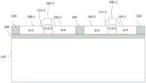
在对背衬底层107减薄之后,执行S11,对该背衬底层107进行刻蚀,具体如图2c所示,保留背衬底层107中与该器件层的每个目标MOS器件的源极正对的第一背衬底层区域和每个目标MOS器件的漏极正对的第二背衬底层区域,由图中所示具体是保留目标MOS管1的源极100-1正对方向的第一背衬底层区域,即图示中的109-1区域,以及目标MOS管1的漏极102-1正对方向的第二背衬底层区域,即图示中的119-1区域,以及目标MOS管2的源极100-2正对方向的第一背衬底层区域,即图示中的109-2区域,以及目标MOS管2的漏极102-2正对方向的第二背衬底层区域,即图示中的119-2区域;刻蚀掉背衬底层中除第一背衬底层区域和第二背衬底层区域之外的其他区域,形成隔离区域。具体是相邻的第一背衬底层区域和第二背衬底层区域之间的第一区域、相邻的第一背衬底层区域之间的第二区域、相邻的第二背衬底层区域之间的第三区域。由图中所示具体是场区103和目标MOS管1的沟道区111-1、场区104、105以及MOS管2的沟道区111-2分别正对方向的背衬底层区域。After the
刻蚀之后,使得第一背衬底层区域完全覆盖该目标MOS器件的源极正对方向的区域,使得第二背衬底层区域完全覆盖该目标MOS器件的漏极正对方向的区域。After etching, the first back substrate layer region completely covers the source-facing region of the target MOS device, and the second back-substrate layer region completely covers the target MOS device drain-facing region.
在本发明实施方式中,将第一背衬底层区域和第二背衬底层区域适当扩宽,是为了避免该第一背衬底层区域和第二背衬底层区域宽度不够,无法制备第一接触孔和第二接触孔,进而能够保证在扩宽的第一背衬底层区域上可以制备第一接触孔,在第二背衬底层区域上可以制作第二接触孔。In the embodiment of the present invention, the area of the first backing layer and the area of the second backing layer are appropriately widened, in order to avoid that the width of the first and second backing layer areas is not enough to prepare the first contact The hole and the second contact hole can further ensure that the first contact hole can be formed on the widened region of the first backing substrate layer, and the second contact hole can be formed on the region of the second backing substrate layer.
上述采用的刻蚀方法具体为如下任意一种刻蚀方法:The etching method adopted above is specifically any one of the following etching methods:
湿法刻蚀、等离子体刻蚀、反应离子刻蚀,电子回旋共振刻蚀、感应耦合等离子刻蚀。当然,并不限定这几种刻蚀方法。Wet etching, plasma etching, reactive ion etching, electron cyclotron resonance etching, inductively coupled plasma etching. Of course, these etching methods are not limited.
在具体的刻蚀过程中,通过淀积光刻胶,曝光、显影后,将背衬底层107中与该器件层的目标MOS管1的源极正对方向的第一背衬底层区域109-1、目标MOS管1的漏极正对方向的第二背衬底层区域119-1以及目标MOS管2的源极正对方向的第一背衬底层区域109-2、目标MOS管2的漏极正对方向的第二背衬底层区域119-2保留,使得裸露出背衬底层107中除了第一背衬底层区域109-1、109-2和第二背衬底区域119-1、119-2之外的其他区域,从而对该裸露出的区域进行刻蚀,并刻蚀至该第一绝缘层106,使得背衬底层107形成多个独立的第一背衬底层区域和第二背衬底层区域,具体是109-1、109-2区域和119-1、119-2区域。In the specific etching process, by depositing photoresist, after exposure and development, the first back substrate layer region 109- 1. The second back substrate layer region 119-1 in the direction facing the drain of the target MOS transistor 1 and the first back substrate layer region 109-2 in the direction facing the source electrode of the target MOS transistor 2, and the drain of the target MOS transistor 2 The second back substrate layer region 119-2 in the very opposite direction remains, so that the
刻蚀之后保留了每个目标MOS器件源极正对的第一背衬底层区域,以及每个目标MOS器件漏极正对的第二背衬底层区域,在有效进行性能调节,促进沟道区散热的同时,还可以减小目标MOS器件源极和漏极的寄生电容,提高了目标MOS器件响应速度。After the etching, the first back substrate layer region facing the source electrode of each target MOS device and the second back substrate layer region facing the drain electrode of each target MOS device are retained, which can effectively adjust the performance and promote the channel region. While dissipating heat, the parasitic capacitance of the source and drain of the target MOS device can also be reduced, thereby improving the response speed of the target MOS device.
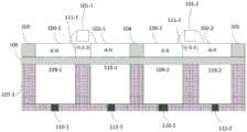
在对背衬底层刻蚀之后,执行S12,如图2d所示,在第一背衬底层区域109-1、109-2和第二背衬底层区域119-1、119-2上形成第二绝缘层107-1,使其填充该隔离区域。After the back substrate layer is etched, S12 is performed. As shown in FIG. 2d, a second back substrate layer is formed on the first back substrate layer regions 109-1 and 109-2 and the second back substrate layer regions 119-1 and 119-2. The insulating layer 107-1 is formed to fill the isolation region.
可以采用淀积方法,该淀积方法具体是采用如下任意一种淀积方法在该第一背衬底层区域表面和第二背衬底层区域表面淀积第二绝缘层107-1:A deposition method can be used. Specifically, the deposition method is to deposit the second insulating layer 107-1 on the surface of the first back substrate layer region and the surface of the second back substrate layer region by any of the following deposition methods:
低压力化学气相沉积法(LPCVD)、等离子化学气相沉积法(PECVD)、常压化学气相沉积法(APCVD),当然,并不限定这几种淀积方法。Low pressure chemical vapor deposition (LPCVD), plasma chemical vapor deposition (PECVD), atmospheric pressure chemical vapor deposition (APCVD), of course, these deposition methods are not limited.
在形成第二绝缘层107-1的过程中还包括将该第二绝缘层107-1平坦化,具体可以是回流、旋涂,或者反应刻蚀平坦化或者化学机械平坦化,使得保留的各第一背衬底层区域之间形成全介质电隔离,当然,并不仅限于上述的几种平坦化方法。The process of forming the second insulating layer 107-1 also includes planarizing the second insulating layer 107-1, specifically, reflow, spin coating, or reactive etching planarization or chemical mechanical planarization, so that the remaining All-dielectric electrical isolation is formed between the regions of the first backing layer, and of course, it is not limited to the above-mentioned several planarization methods.
最后,执行S13,如图2e、图2f、图2g所示,形成从该第二绝缘层107-1表面连通该第一背衬底层区域109-1、109-2的第一接触孔,形成从该第二绝缘层107-1表面连通该第二背衬底层区域119-1、119-2的第二接触孔,采用导电材料填充每个第一接触孔和每个第二接触孔,并在第二绝缘层107-1表面形成每个接触孔的导电结构。Finally, S13 is performed, as shown in FIG. 2e, FIG. 2f, and FIG. 2g, forming a first contact hole connecting the first back substrate layer regions 109-1 and 109-2 from the surface of the second insulating layer 107-1, forming The second contact holes of the second back substrate layer regions 119-1 and 119-2 are communicated from the surface of the second insulating layer 107-1, and each first contact hole and each second contact hole are filled with a conductive material, and A conductive structure of each contact hole is formed on the surface of the second insulating layer 107-1.
在该第一接触孔、第二接触孔采用淀积方法填充导电材料,具体如图2f、如图2g所示的110-1、110-2、111-1、111-2区域,并在该第二绝缘层107-1表面形成每个接触孔的导电结构,通过该导电结构实现对第一背衬底层区域、第二背衬底层区域电压的调节控制。The first contact hole and the second contact hole are filled with conductive material by deposition method, specifically the regions 110-1, 110-2, 111-1 and 111-2 as shown in FIG. 2f and FIG. A conductive structure of each contact hole is formed on the surface of the second insulating layer 107-1, and the voltage regulation and control of the first back substrate layer region and the second back substrate layer region are realized through the conductive structure.
具体地,从该第二绝缘层107-1向该第一背衬底层区域109-1、109-2正下方分别刻蚀第一接触孔,淀积导电材料110-1、111-1、110-2、111-2(如钨),若109-1和119-1、109-2和119-2掺杂浓度较低,无法同导电材料110-1、111-1、110-2、111-2形成欧姆接触,则还需要在淀积导电材料110-1、111-1、110-2、111-2之前,通过接触孔对第一背衬底层区域109-1,109-2以及第二背衬底层区域119-1、119-2进行重掺杂,以实现第一背衬底层区域和导电材料,第二背衬底和导电材料的欧姆接触。Specifically, the first contact holes are respectively etched from the second insulating layer 107-1 to directly below the first back substrate layer regions 109-1 and 109-2, and conductive materials 110-1, 111-1 and 110 are deposited. -2, 111-2 (such as tungsten), if the doping concentration of 109-1 and 119-1, 109-2 and 119-2 is low, it cannot be compared with the conductive materials 110-1, 111-1, 110-2, 111 -2 to form an ohmic contact, it is also necessary to connect the first back substrate layer regions 109-1, 109-2 and the first back substrate layer regions 109-1, 109-2 and the first back substrate layer regions 109-1, 109-2 and the first back substrate layer regions 109-1, 109-2 and the third The two back substrate layer regions 119-1 and 119-2 are heavily doped to realize ohmic contact between the first back substrate layer region and the conductive material, and the second back substrate layer and the conductive material.
从该第二绝缘层107-1向该第二背衬底层区域119-1和119-2正下方分别刻蚀第二接触孔,然后,光刻该第一接触孔和第二接触孔,在该第一接触孔淀积导电材料,在第二接触孔淀积导电材料,具体是形成如图2g所示的110-1、110-2、111-1、111-2区域,淀积钝化层及插键孔(PAD)开窗,形成第一背衬底层区域和导电材料的欧姆接触,以及第二背衬底层区域和导电材料的欧姆接触,再在该第二绝缘层107-1表面形成每个接触孔的导电结构,该导电结构,具体可以是导电层,该导电层一对应连接导电材料110-1,该导电层二对应连接导电材料110-2,导电层三对应连接导电材料111-1,导电层四对应连接导电材料111-2,通过该导电结构可实现第一背衬底层区域、第二背衬底层区域分别与芯片外部的电信号连接,通过该导电结构实现对第一背衬底层区域、第二背衬底层区域电压的调节控制。当然,每个导电结构也可相互连接,同时也可淀积钝化层材料之后通过钝化层的PAD开槽,将两者的电学参数引出到芯片外部进行电连接。The second contact holes are respectively etched from the second insulating layer 107-1 to directly below the second back substrate layer regions 119-1 and 119-2, and then the first contact hole and the second contact hole are etched by photolithography. Conductive material is deposited in the first contact hole, and conductive material is deposited in the second contact hole, specifically forming regions 110-1, 110-2, 111-1, and 111-2 as shown in FIG. 2g, and depositing passivation Layer and key hole (PAD) windows are formed to form the ohmic contact between the first back substrate layer region and the conductive material, as well as the ohmic contact between the second back substrate layer region and the conductive material, and then on the surface of the second insulating layer 107-1 A conductive structure is formed for each contact hole. Specifically, the conductive structure can be a conductive layer. One of the conductive layers is connected to the conductive material 110-1, the second of the conductive layer is connected to the conductive material 110-2, and the third of the conductive layer is connected to the conductive material. 111-1, the conductive layer 4 is connected to the conductive material 111-2 correspondingly. Through this conductive structure, the first back substrate layer area and the second back substrate layer area can be respectively connected to the electrical signals outside the chip. Adjustment and control of voltages in a backing substrate layer region and a second backing substrate layer region. Of course, each conductive structure can also be connected to each other, and at the same time, after depositing the passivation layer material, the PAD of the passivation layer can be used to make grooves, and the electrical parameters of the two can be extracted to the outside of the chip for electrical connection.
具体该导电材料和导电结构均可采用如下任意一种材料:Specifically, the conductive material and the conductive structure can be any of the following materials:
金属、合金、无机非金属。Metals, alloys, inorganic non-metals.
通过该导电结构调节各第一背衬底层区域的电压值以及第二背衬底层区域,从而控制其上方的MOS器件的阈值电压,对该MOS器件参数进行优化调整,抵消辐照对该SOI半导体产生的不良影响,提高了该器件的抗辐照性能。The voltage value of each first back substrate layer region and the second back substrate layer region are adjusted by the conductive structure, so as to control the threshold voltage of the MOS device above it, optimize the adjustment of the parameters of the MOS device, and cancel the irradiation of the SOI semiconductor. The resulting adverse effects improve the anti-radiation performance of the device.
而且,相邻的第一背衬底层区域和第二背衬底层区域之间、相邻的第一背衬底层区域之间、相邻的第二背衬底层区域之间均采用第二绝缘层进行全介质隔离,全介质隔离的击穿电压更高。因此,本发明中的SOI器件结构的背衬底电压取值范围更大,对器件性能的调控力度就更大,使得器件抗辐照性能更强。Moreover, a second insulating layer is used between the adjacent first backing layer regions and the second backing layer regions, between the adjacent first backing layer regions, and between the adjacent second backing layer regions. Perform full dielectric isolation, and the breakdown voltage of full dielectric isolation is higher. Therefore, the back-substrate voltage of the SOI device structure in the present invention has a larger value range, and the control strength of the device performance is greater, so that the device has a stronger radiation resistance performance.
再者,通过在每个MOS器件的源极正对下方的第一背衬底层由导电结构引出信号线以及每个MOS器件的漏极正对下方的第二背衬底层由导电结构引出信号线,与其他器件芯片是在芯片上方走线引出的方式不同,有效减小了芯片上方的走线压力,降低了芯片的面积,减小了芯片的成本。Furthermore, the signal lines are led out from the conductive structure through the first back substrate layer directly under the source electrode of each MOS device and the signal lines are led out from the conductive structure through the second back substrate layer directly under the drain electrode of each MOS device. , which is different from the way that other device chips are routed above the chip, which effectively reduces the wiring pressure above the chip, reduces the area of the chip, and reduces the cost of the chip.
在本发明实施例中第一绝缘层和第二绝缘层均采用如下任意一种绝缘材料:In the embodiment of the present invention, the first insulating layer and the second insulating layer both adopt any one of the following insulating materials:
二氧化硅、氮化硅、玻璃。当然,并不限定这几种材料。Silicon dioxide, silicon nitride, glass. Of course, these materials are not limited.
该器件层和第一背衬底层区域、第二背衬底层区域均采用如下任意一种半导体材料:The device layer, the first back substrate layer region, and the second back substrate layer region all use any one of the following semiconductor materials:
硅、砷化镓、氮化镓、碳化硅。当然,并不限定这几种材料。Silicon, Gallium Arsenide, Gallium Nitride, Silicon Carbide. Of course, these materials are not limited.
其中,由于该背衬底层材料为高掺杂的半导体材料,因此,该第一背衬底层区域材料和第二背衬底层区域材料为高掺杂半导体材料,其掺杂浓度能够使得背衬底层与接触孔处的导电材料形成欧姆接触。Wherein, since the material of the backing substrate layer is a highly doped semiconductor material, the material of the first backing substrate layer region and the material of the second backing substrate layer region are highly doped semiconductor materials, and their doping concentration can make the backing substrate layer An ohmic contact is formed with the conductive material at the contact hole.
若该背衬底层材料是低掺杂的半导体材料,可采用光刻和扩散,在形成的第一背衬底层区域和第二背衬底层区域分别形成接触孔的位置形成局部高掺杂的区域,具体如图2f所示的108-1、118-1、108-2、118-2区域,用于实现第一背衬底层区域与导电材料的欧姆接触,第二背衬底层区域与导电材料的欧姆接触。If the material of the backing layer is a low-doped semiconductor material, photolithography and diffusion can be used to form locally highly doped regions at the positions where the contact holes are formed in the first backing layer region and the second backing layer region respectively. , specifically the 108-1, 118-1, 108-2, 118-2 regions as shown in Figure 2f are used to realize the ohmic contact between the first backing substrate layer region and the conductive material, and the second backing substrate layer region and the conductive material. ohmic contact.
实施例二Embodiment 2
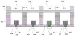
在本发明第一实施例提供了一种SOI器件结构,如图3所示,包括:The first embodiment of the present invention provides an SOI device structure, as shown in FIG. 3 , including:
第一绝缘层301;the first insulating
位于所述第一绝缘层301上方的器件层,所述器件层用于制备多个目标MOS器件;a device layer above the first insulating
在所述第一绝缘层301下方正对每个目标MOS器件的源极302均有第一背衬底层304,在所述第一绝缘层301下方正对每个目标MOS器件的漏极303均有第二背衬底层305;There is a first
在每个所述第一背衬底层304的表面、每个所述第二背衬底层305的表面以及相邻的第一背衬底层304之间、相邻的第二背衬底层305之间以及相邻的第一背衬底层304和第二背衬底层305之间均隔离有第二绝缘层306;Between the surface of each of the first backing layers 304 , the surface of each of the second backing layers 305 , and between adjacent first backing layers 304 and between adjacent second backing layers 305 and a second insulating
每个所述第一背衬底层304下方有连通所述第二绝缘层306的第一接触孔,正对每个所述第二背衬底层305下方有连通所述第二绝缘层306的第二接触孔;Below each of the first backing substrate layers 304 is a first contact hole communicating with the second insulating
每个所述第一接触孔和每个所述第二接触孔内均填充有导电材料307;Each of the first contact holes and each of the second contact holes is filled with
在所述第二绝缘层表面形成每个接触孔的导电结构308。A
在具体的实施方式中,所述第一背衬底层完全覆盖所述目标MOS器件的源极正对方向的区域,所述第二背衬底层完全覆盖所述目标MOS器件的漏极正对方向的区域。In a specific embodiment, the first back substrate layer completely covers the source-facing direction of the target MOS device, and the second back substrate layer completely covers the drain-facing direction of the target MOS device Area.
在具体的实施方式中,所述第一绝缘层301、第二绝缘层305均采用如下任意一种绝缘材料:In a specific implementation manner, the first insulating
二氧化硅、氮化硅、玻璃。Silicon dioxide, silicon nitride, glass.
所述第一背衬底层304和所述器件层具体采用如下任意一种半导体材料:The first
硅、砷化镓、氮化镓、碳化硅。Silicon, Gallium Arsenide, Gallium Nitride, Silicon Carbide.
其中,该第一背衬底层、第二背衬底层材料为高掺杂半导体材料,其掺杂浓度能够使得第一背衬底层304与第一接触孔处的导电材料307,第二背衬底层与第二接触孔处的导电材料形成欧姆接触。The materials of the first backing layer and the second backing layer are highly doped semiconductor materials, and the doping concentration can make the
若该背衬底层材料是低掺杂的半导体材料,可采用光刻和扩散,在形成的第一背衬底层和第二背衬底层分别形成接触孔的位置形成局部高掺杂的区域,具体如图3所示的308区域,用于实现第一背衬底层与导电材料的欧姆接触,第二背衬底层与导电材料的欧姆接触。If the material of the backing layer is a low-doped semiconductor material, photolithography and diffusion can be used to form locally highly doped regions at the positions where the contact holes are formed in the first backing layer and the second backing layer respectively. The
本发明实施例中的一个或多个技术方案,至少具有如下技术效果或优点:One or more technical solutions in the embodiments of the present invention have at least the following technical effects or advantages:
本发明提供一种SOI器件结构的制备方法,该SOI器件结构包括由下至上的背衬底层、第一绝缘层、器件层,包括:对背衬底层进行刻蚀,保留背衬底层中与器件层的每个MOS器件的源极正对的第一背衬底层区域和每个MOS器件的漏极正对的第二背衬底层区域,刻蚀掉多个MOS器件正对下方的背衬底层中相邻的第一背衬底层区域和第二背衬底层区域之间的第一区域、相邻的第一背衬底层区域之间的第二区域、以及相邻的第二背衬底层区域之间的第三区域,形成隔离区域;在第一背衬底层和第二背衬底层上形成第二绝缘层,使其填充隔离区域;形成从第二绝缘层表面连通每个第一背衬底层的第一接触孔和形成从第二绝缘层表面连通每个第二背衬底层的第二接触孔,采用导电材料填充每个第一接触孔和每个第二接触孔,并在第二绝缘层表面形成每个接触孔的导电结构,该制备工艺中完整保留了原有器件的结构,仅在背衬底层上通过隔离刻蚀的方法,将器件结构的每个器件的源极正对方向的第一背衬底层和漏极正对方向的第二背衬底层分别隔离,形成单独的第一背衬底层底部和单独的第二背衬底层底部连接外部的导电结构,从器件的背部引出导线,由两个端口对背衬底的电压进行调节控制,更加灵活,极大地减小芯片的设计和制造成本,简化了工艺,同时还可以提高器件抗辐照性能。The invention provides a preparation method of an SOI device structure. The SOI device structure includes a bottom-up backing substrate layer, a first insulating layer, and a device layer, including: etching the backing substrate layer, and retaining the backing substrate layer and the device The source of each MOS device is directly opposite to the first back substrate layer region and the drain of each MOS device is directly opposite to the second back substrate layer region, and the back substrate layer directly below the plurality of MOS devices is etched away A first region between adjacent first and second backing layer regions, a second region between adjacent first backing layer regions, and an adjacent second backing layer region A third area between the two, forming an isolation area; forming a second insulating layer on the first backing substrate layer and the second backing substrate layer, so that it fills the isolation area; forming a connection from the surface of the second insulating layer to each first backing A first contact hole of the bottom layer and a second contact hole formed from the surface of the second insulating layer to communicate with each second backing substrate layer, each first contact hole and each second contact hole are filled with a conductive material, and the second contact hole is filled with a conductive material. The conductive structure of each contact hole is formed on the surface of the insulating layer. In this preparation process, the structure of the original device is completely retained, and only the source electrode of each device of the device structure is facing by the method of isolation and etching on the back substrate layer. The first back substrate layer in the direction and the second back substrate layer in the direction opposite to the drain are respectively isolated to form a separate first back substrate layer bottom and a separate second back substrate layer bottom to connect the external conductive structure, from the back of the device The lead-out wire is adjusted and controlled by two ports to control the voltage of the back substrate, which is more flexible, greatly reduces the design and manufacturing cost of the chip, simplifies the process, and can also improve the radiation resistance of the device.
尽管已描述了本发明的优选实施例,但本领域内的技术人员一旦得知了基本创造性概念,则可对这些实施例作出另外的变更和修改。所以,所附权利要求意欲解释为包括优选实施例以及落入本发明范围的所有变更和修改。Although preferred embodiments of the present invention have been described, additional changes and modifications to these embodiments may occur to those skilled in the art once the basic inventive concepts are known. Therefore, the appended claims are intended to be construed to include the preferred embodiment and all changes and modifications that fall within the scope of the present invention.
显然,本领域的技术人员可以对本发明进行各种改动和变型而不脱离本发明的精神和范围。这样,倘若本发明的这些修改和变型属于本发明权利要求及其等同技术的范围之内,则本发明也意图包含这些改动和变型在内。It will be apparent to those skilled in the art that various modifications and variations can be made in the present invention without departing from the spirit and scope of the invention. Thus, provided that these modifications and variations of the present invention fall within the scope of the claims of the present invention and their equivalents, the present invention is also intended to include these modifications and variations.
Claims (10)
Translated fromChinesePriority Applications (1)
| Application Number | Priority Date | Filing Date | Title |
|---|---|---|---|
| CN201910011393.9ACN109801847B (en) | 2019-01-07 | 2019-01-07 | A kind of SOI device structure and preparation method thereof |
Applications Claiming Priority (1)
| Application Number | Priority Date | Filing Date | Title |
|---|---|---|---|
| CN201910011393.9ACN109801847B (en) | 2019-01-07 | 2019-01-07 | A kind of SOI device structure and preparation method thereof |
Publications (2)
| Publication Number | Publication Date |
|---|---|
| CN109801847A CN109801847A (en) | 2019-05-24 |
| CN109801847Btrue CN109801847B (en) | 2020-06-23 |
Family
ID=66558499
Family Applications (1)
| Application Number | Title | Priority Date | Filing Date |
|---|---|---|---|
| CN201910011393.9AActiveCN109801847B (en) | 2019-01-07 | 2019-01-07 | A kind of SOI device structure and preparation method thereof |
Country Status (1)
| Country | Link |
|---|---|
| CN (1) | CN109801847B (en) |
Citations (3)
| Publication number | Priority date | Publication date | Assignee | Title |
|---|---|---|---|---|
| CN102361031A (en)* | 2011-10-19 | 2012-02-22 | 电子科技大学 | Semiconductor device used for SOI (silicon-on-insulator) high-voltage integrated circuit |
| CN102437087A (en)* | 2011-12-14 | 2012-05-02 | 中国科学院微电子研究所 | Radiation-resistant and reinforced SOI structure and its manufacturing method |
| CN103022139A (en)* | 2012-12-28 | 2013-04-03 | 上海集成电路研发中心有限公司 | Semiconductor structure with insulating buried layer and manufacturing method thereof |
Family Cites Families (1)
| Publication number | Priority date | Publication date | Assignee | Title |
|---|---|---|---|---|
| JP2009194157A (en)* | 2008-02-14 | 2009-08-27 | Oki Semiconductor Co Ltd | Manufacturing method of semiconductor device |
- 2019
- 2019-01-07CNCN201910011393.9Apatent/CN109801847B/enactiveActive
Patent Citations (3)
| Publication number | Priority date | Publication date | Assignee | Title |
|---|---|---|---|---|
| CN102361031A (en)* | 2011-10-19 | 2012-02-22 | 电子科技大学 | Semiconductor device used for SOI (silicon-on-insulator) high-voltage integrated circuit |
| CN102437087A (en)* | 2011-12-14 | 2012-05-02 | 中国科学院微电子研究所 | Radiation-resistant and reinforced SOI structure and its manufacturing method |
| CN103022139A (en)* | 2012-12-28 | 2013-04-03 | 上海集成电路研发中心有限公司 | Semiconductor structure with insulating buried layer and manufacturing method thereof |
Also Published As
| Publication number | Publication date |
|---|---|
| CN109801847A (en) | 2019-05-24 |
Similar Documents
| Publication | Publication Date | Title |
|---|---|---|
| JP3489936B2 (en) | Method of manufacturing MOS transistor having SOI structure | |
| US10916468B2 (en) | Semiconductor device with buried local interconnects | |
| TW202141655A (en) | Semiconductor devices and method of forming the same | |
| JP5637632B2 (en) | RF apparatus and method featuring grooves under bond pads | |
| TW202145517A (en) | Three-dimensional memory device and method for forming the same | |
| TWI753602B (en) | Three-dimensional memory devices with supporting structure for staircase region | |
| TW201705478A (en) | Vertical semiconductor component with thin substrate | |
| TW202009986A (en) | Semiconductor-on-insulator (SOI) substrate and method for forming same | |
| US20200135921A1 (en) | Multi-channel device to improve transistor speed | |
| JP2025000927A (en) | Method for forming contact structure, and its semiconductor device | |
| CN111508963B (en) | Peripheral circuit, three-dimensional memory and preparation method thereof | |
| CN111276542B (en) | Groove type MOS device and manufacturing method thereof | |
| JP7519992B2 (en) | Semiconductor vertical Schottky diode and method of manufacture thereof | |
| CN109841561B (en) | A kind of SOI device structure and preparation method thereof | |
| KR20030026912A (en) | High-voltage periphery | |
| CN109801847B (en) | A kind of SOI device structure and preparation method thereof | |
| CN109524355B (en) | Structure and forming method of semiconductor device | |
| US10304839B2 (en) | Metal strap for DRAM/FinFET combination | |
| CN109860098B (en) | A kind of SOI device structure and preparation method thereof | |
| CN109560065B (en) | A semiconductor device structure and forming method with body contact | |
| TW202221908A (en) | Method for forming three-dimensional memory device | |
| CN109545785B (en) | Semiconductor device structure and preparation method | |
| CN109616472B (en) | Semiconductor device structure and forming method | |
| CN111312809B (en) | Power device and method of making the same | |
| CN110943066A (en) | Semiconductor structure with high resistance wafer and bonding method of high resistance wafer |
Legal Events
| Date | Code | Title | Description |
|---|---|---|---|
| PB01 | Publication | ||
| PB01 | Publication | ||
| SE01 | Entry into force of request for substantive examination | ||
| SE01 | Entry into force of request for substantive examination | ||
| GR01 | Patent grant | ||
| GR01 | Patent grant |