CN109754757B - Pixel driving circuit, display device and pixel driving method - Google Patents
Pixel driving circuit, display device and pixel driving methodDownload PDFInfo
- Publication number
- CN109754757B CN109754757BCN201910243634.2ACN201910243634ACN109754757BCN 109754757 BCN109754757 BCN 109754757BCN 201910243634 ACN201910243634 ACN 201910243634ACN 109754757 BCN109754757 BCN 109754757B
- Authority
- CN
- China
- Prior art keywords
- switch module
- electrically connected
- transistor
- module
- node
- Prior art date
- Legal status (The legal status is an assumption and is not a legal conclusion. Google has not performed a legal analysis and makes no representation as to the accuracy of the status listed.)
- Active
Links
Images


Classifications
- G—PHYSICS
- G09—EDUCATION; CRYPTOGRAPHY; DISPLAY; ADVERTISING; SEALS
- G09G—ARRANGEMENTS OR CIRCUITS FOR CONTROL OF INDICATING DEVICES USING STATIC MEANS TO PRESENT VARIABLE INFORMATION
- G09G3/00—Control arrangements or circuits, of interest only in connection with visual indicators other than cathode-ray tubes
- G09G3/20—Control arrangements or circuits, of interest only in connection with visual indicators other than cathode-ray tubes for presentation of an assembly of a number of characters, e.g. a page, by composing the assembly by combination of individual elements arranged in a matrix no fixed position being assigned to or needed to be assigned to the individual characters or partial characters
- G09G3/22—Control arrangements or circuits, of interest only in connection with visual indicators other than cathode-ray tubes for presentation of an assembly of a number of characters, e.g. a page, by composing the assembly by combination of individual elements arranged in a matrix no fixed position being assigned to or needed to be assigned to the individual characters or partial characters using controlled light sources
- G09G3/30—Control arrangements or circuits, of interest only in connection with visual indicators other than cathode-ray tubes for presentation of an assembly of a number of characters, e.g. a page, by composing the assembly by combination of individual elements arranged in a matrix no fixed position being assigned to or needed to be assigned to the individual characters or partial characters using controlled light sources using electroluminescent panels
- G09G3/32—Control arrangements or circuits, of interest only in connection with visual indicators other than cathode-ray tubes for presentation of an assembly of a number of characters, e.g. a page, by composing the assembly by combination of individual elements arranged in a matrix no fixed position being assigned to or needed to be assigned to the individual characters or partial characters using controlled light sources using electroluminescent panels semiconductive, e.g. using light-emitting diodes [LED]
- G09G3/3208—Control arrangements or circuits, of interest only in connection with visual indicators other than cathode-ray tubes for presentation of an assembly of a number of characters, e.g. a page, by composing the assembly by combination of individual elements arranged in a matrix no fixed position being assigned to or needed to be assigned to the individual characters or partial characters using controlled light sources using electroluminescent panels semiconductive, e.g. using light-emitting diodes [LED] organic, e.g. using organic light-emitting diodes [OLED]
- G09G3/3225—Control arrangements or circuits, of interest only in connection with visual indicators other than cathode-ray tubes for presentation of an assembly of a number of characters, e.g. a page, by composing the assembly by combination of individual elements arranged in a matrix no fixed position being assigned to or needed to be assigned to the individual characters or partial characters using controlled light sources using electroluminescent panels semiconductive, e.g. using light-emitting diodes [LED] organic, e.g. using organic light-emitting diodes [OLED] using an active matrix
- G09G3/3233—Control arrangements or circuits, of interest only in connection with visual indicators other than cathode-ray tubes for presentation of an assembly of a number of characters, e.g. a page, by composing the assembly by combination of individual elements arranged in a matrix no fixed position being assigned to or needed to be assigned to the individual characters or partial characters using controlled light sources using electroluminescent panels semiconductive, e.g. using light-emitting diodes [LED] organic, e.g. using organic light-emitting diodes [OLED] using an active matrix with pixel circuitry controlling the current through the light-emitting element
- G—PHYSICS
- G09—EDUCATION; CRYPTOGRAPHY; DISPLAY; ADVERTISING; SEALS
- G09G—ARRANGEMENTS OR CIRCUITS FOR CONTROL OF INDICATING DEVICES USING STATIC MEANS TO PRESENT VARIABLE INFORMATION
- G09G3/00—Control arrangements or circuits, of interest only in connection with visual indicators other than cathode-ray tubes
- G09G3/20—Control arrangements or circuits, of interest only in connection with visual indicators other than cathode-ray tubes for presentation of an assembly of a number of characters, e.g. a page, by composing the assembly by combination of individual elements arranged in a matrix no fixed position being assigned to or needed to be assigned to the individual characters or partial characters
- G09G3/22—Control arrangements or circuits, of interest only in connection with visual indicators other than cathode-ray tubes for presentation of an assembly of a number of characters, e.g. a page, by composing the assembly by combination of individual elements arranged in a matrix no fixed position being assigned to or needed to be assigned to the individual characters or partial characters using controlled light sources
- G09G3/30—Control arrangements or circuits, of interest only in connection with visual indicators other than cathode-ray tubes for presentation of an assembly of a number of characters, e.g. a page, by composing the assembly by combination of individual elements arranged in a matrix no fixed position being assigned to or needed to be assigned to the individual characters or partial characters using controlled light sources using electroluminescent panels
- G09G3/32—Control arrangements or circuits, of interest only in connection with visual indicators other than cathode-ray tubes for presentation of an assembly of a number of characters, e.g. a page, by composing the assembly by combination of individual elements arranged in a matrix no fixed position being assigned to or needed to be assigned to the individual characters or partial characters using controlled light sources using electroluminescent panels semiconductive, e.g. using light-emitting diodes [LED]
- G09G3/3208—Control arrangements or circuits, of interest only in connection with visual indicators other than cathode-ray tubes for presentation of an assembly of a number of characters, e.g. a page, by composing the assembly by combination of individual elements arranged in a matrix no fixed position being assigned to or needed to be assigned to the individual characters or partial characters using controlled light sources using electroluminescent panels semiconductive, e.g. using light-emitting diodes [LED] organic, e.g. using organic light-emitting diodes [OLED]
- G09G3/3275—Details of drivers for data electrodes
- G09G3/3291—Details of drivers for data electrodes in which the data driver supplies a variable data voltage for setting the current through, or the voltage across, the light-emitting elements
Landscapes
- Engineering & Computer Science (AREA)
- Physics & Mathematics (AREA)
- Computer Hardware Design (AREA)
- General Physics & Mathematics (AREA)
- Theoretical Computer Science (AREA)
- Control Of Indicators Other Than Cathode Ray Tubes (AREA)
- Control Of El Displays (AREA)
- Electroluminescent Light Sources (AREA)
Abstract
Translated fromChinese
Description
Translated fromChinese技术领域technical field
本申请涉及显示技术领域,具体而言,本申请涉及一种像素驱动电路、显示装置及像素驱动方法。The present application relates to the field of display technology, and in particular, the present application relates to a pixel driving circuit, a display device and a pixel driving method.
背景技术Background technique
有机发光二极管(OLED,Organic Light-Emitting Diode)作为一种电流型发光器件已越来越多地被应用于新一代显示装置中。Organic Light-Emitting Diode (OLED, Organic Light-Emitting Diode), as a current-type light-emitting device, has been increasingly used in new-generation display devices.
基础的OLED驱动电路为2T1C,驱动电流(即流过驱动晶体管的电流)的值可决定OLED器件所产生的亮度,驱动电流的大小与驱动晶体管的阈值电压有关。The basic OLED driving circuit is 2T1C. The value of the driving current (that is, the current flowing through the driving transistor) can determine the brightness generated by the OLED device. The magnitude of the driving current is related to the threshold voltage of the driving transistor.
由于晶体管的制程因素,在显示装置各区域的晶体管的特性会存在差异,即驱动晶体管的阈值电压存在差异。因此,当不同区域的多个显示单元写入相同的数据信号时,驱动晶体管提供给OLED器件不同的驱动电流,导致显示装置亮度显示不均。Due to the process factors of the transistors, the characteristics of the transistors in various regions of the display device may be different, that is, the threshold voltages of the driving transistors may be different. Therefore, when the same data signal is written to a plurality of display units in different regions, the driving transistors provide different driving currents to the OLED devices, resulting in uneven brightness display of the display device.
发明内容SUMMARY OF THE INVENTION
本申请针对现有方式的缺点,提出一种像素驱动电路、显示装置及像素驱动方法,用以解决现有技术存在的由于驱动晶体管的阈值电压存在差异导致OLED器件的驱动电流不稳定以及显示亮度不均的技术问题。Aiming at the shortcomings of the existing methods, the present application proposes a pixel driving circuit, a display device and a pixel driving method, which are used to solve the problems in the prior art that the driving current of the OLED device is unstable due to the difference in the threshold voltage of the driving transistor and the display brightness is not stable. Uneven technical issues.
第一方面,本申请实施例提供了一种像素驱动电路,包括:电荷存储模块、驱动模块、第一开关模块、第二开关模块和第三开关模块;In a first aspect, an embodiment of the present application provides a pixel driving circuit, including: a charge storage module, a driving module, a first switch module, a second switch module, and a third switch module;
电荷存储模块的第一端与第一电压端电连接,第二端与第一节点电连接,第三端与第二节点电连接;The first terminal of the charge storage module is electrically connected to the first voltage terminal, the second terminal is electrically connected to the first node, and the third terminal is electrically connected to the second node;
驱动模块的第一端与第一节点电连接,第二端与第二节点电连接;The first end of the driving module is electrically connected to the first node, and the second end is electrically connected to the second node;
第一开关模块的第一端与扫描信号线电连接,第二端与数据信号线电连接,第三端与第二节点电连接,第四端与第一节点电连接,第五端与第三节点电连接;The first end of the first switch module is electrically connected to the scan signal line, the second end is electrically connected to the data signal line, the third end is electrically connected to the second node, the fourth end is electrically connected to the first node, and the fifth end is electrically connected to the first node. Three-node electrical connection;
第二开关模块的第一端与第一控制信号线电连接,第二端与第一电压端电连接,第三端与第三节点电连接,第四端与第二节点电连接,第五端与发光元件电连接;The first terminal of the second switch module is electrically connected to the first control signal line, the second terminal is electrically connected to the first voltage terminal, the third terminal is electrically connected to the third node, the fourth terminal is electrically connected to the second node, and the fifth terminal is electrically connected to the second node. The terminal is electrically connected with the light-emitting element;
第三开关模块的第一端与第二控制信号线电连接,第二端与第三节点电连接,第三端与驱动模块的第三端电连接。The first end of the third switch module is electrically connected to the second control signal line, the second end is electrically connected to the third node, and the third end is electrically connected to the third end of the driving module.
第二方面,本申请实施例提供了一种显示装置,包括本申请实施例提供的像素驱动电路。In a second aspect, the embodiments of the present application provide a display device including the pixel driving circuit provided by the embodiments of the present application.
第三方面,本申请实施例提供了一种像素驱动方法,应用于本申请实施例提供的像素驱动电路,包括:In a third aspect, the embodiments of the present application provide a pixel driving method, which is applied to the pixel driving circuit provided by the embodiments of the present application, including:
在复位阶段,像素驱动电路中的第一开关模块和第二开关模块,在通过各自的第一端接收到第一电平信号时均导通,将通过第二开关模块的第二端接收到的电源电压和通过第一开关模块的第二端接收到的初始信号,分别输出至第一节点和第二节点;In the reset stage, the first switch module and the second switch module in the pixel drive circuit are both turned on when receiving the first level signal through their respective first terminals, and will receive the signal through the second terminal of the second switch module. The power supply voltage and the initial signal received through the second end of the first switch module are respectively output to the first node and the second node;
在补偿阶段,第二开关模块在通过其第一端接收到第二电平信号时断开,第一开关模块和像素驱动电路中的第三开关模块,在通过各自的第一端接收到第一电平信号时分别保持导通状态和导通,第一开关模块将通过其第二端接收到的数据信号输出至第二节点,像素驱动电路根据数据信号对驱动模块的阈值电压进行补偿;In the compensation stage, the second switch module is turned off when it receives the second level signal through its first terminal, and the first switch module and the third switch module in the pixel driving circuit receive the second level signal through their respective first terminals. The first switch module outputs the data signal received through its second terminal to the second node, and the pixel driving circuit compensates the threshold voltage of the driving module according to the data signal;
在发光阶段,第一开关模块在通过其第一端接收到第二电平信号时断开,第二开关模块和第三开关模块,在通过各自的第一端接收到第一电平信号时分别导通和保持导通状态,使得像素驱动电路中的驱动模块输出驱动电流至发光元件。In the light-emitting phase, the first switch module is disconnected when receiving the second level signal through its first terminal, and the second switch module and the third switch module are disconnected when receiving the first level signal through their respective first terminals Turn on and maintain the on state respectively, so that the driving module in the pixel driving circuit outputs the driving current to the light-emitting element.
本申请实施例提供的技术方案,至少具有如下有益效果:The technical solutions provided in the embodiments of the present application have at least the following beneficial effects:
1)采用本申请实施例提供的像素驱动电路、显示装置和像素驱动方法,能够有效地对驱动晶体管的阈值电压进行补偿,并具有较好的补偿效果,可降低阈值电压的不稳定对显示亮度的影响,使显示亮度更加稳定、均一性更佳,从而改善显示画面的显示质量。1) By adopting the pixel driving circuit, display device and pixel driving method provided by the embodiments of the present application, the threshold voltage of the driving transistor can be effectively compensated, and the compensation effect is good, and the instability of the threshold voltage can be reduced to the display brightness. The influence of the display brightness is more stable and the uniformity is better, thereby improving the display quality of the display screen.
2)在本申请实施例提供的像素驱动电路工作时,只需要3条栅极驱动线(分别为扫描信号线、第一控制信号线和第二控制信号线),信号波形简单,有利于实现显示装置的GOA(Gate on Array,栅极驱动电路阵列)设计。2) When the pixel driving circuit provided by the embodiment of the present application works, only 3 gate driving lines (respectively, the scanning signal line, the first control signal line and the second control signal line) are required, and the signal waveform is simple, which is conducive to the realization of GOA (Gate on Array, gate drive circuit array) design of a display device.
本申请附加的方面和优点将在下面的描述中部分给出,这些将从下面的描述中变得明显,或通过本申请的实践了解到。Additional aspects and advantages of the present application will be set forth in part in the following description, which will become apparent from the following description, or may be learned by practice of the present application.
附图说明Description of drawings
本申请上述的和/或附加的方面和优点从下面结合附图对实施例的描述中将变得明显和容易理解,其中:The above and/or additional aspects and advantages of the present application will become apparent and readily understood from the following description of embodiments taken in conjunction with the accompanying drawings, wherein:
图1为现有的OLED驱动电路的电路原理示意图;FIG. 1 is a schematic diagram of the circuit principle of an existing OLED driving circuit;
图2为本申请实施例提供的一种像素驱动电路的电路原理示意图;FIG. 2 is a schematic diagram of a circuit principle of a pixel driving circuit provided by an embodiment of the present application;
图3为本申请实施例提供的一种像素驱动方法的流程示意图;FIG. 3 is a schematic flowchart of a pixel driving method provided by an embodiment of the present application;
图4为本申请实施例提供的像素驱动电路的控制信号示意图;FIG. 4 is a schematic diagram of a control signal of a pixel driving circuit provided by an embodiment of the present application;
图5为本申请实施例提供的像素驱动电路和像素驱动方法的补偿效果示意图。FIG. 5 is a schematic diagram of compensation effects of a pixel driving circuit and a pixel driving method provided by an embodiment of the present application.
具体实施方式Detailed ways
下面详细描述本申请,本申请实施例的示例在附图中示出,其中自始至终相同或类似的标号表示相同或类似的部件或具有相同或类似功能的部件。此外,如果已知技术的详细描述对于示出的本申请的特征是不必要的,则将其省略。下面通过参考附图描述的实施例是示例性的,仅用于解释本申请,而不能解释为对本申请的限制。The present application is described in detail below, and examples of embodiments of the present application are illustrated in the accompanying drawings, wherein the same or similar reference numerals refer to the same or similar components or components having the same or similar functions throughout. Also, detailed descriptions of known technologies are omitted if they are not necessary for illustrating features of the present application. The embodiments described below with reference to the accompanying drawings are exemplary and are only used to explain the present application, but not to be construed as a limitation on the present application.
本技术领域技术人员可以理解,除非另外定义,这里使用的所有术语(包括技术术语和科学术语),具有与本申请所属领域中的普通技术人员的一般理解相同的意义。还应该理解的是,诸如通用字典中定义的那些术语,应该被理解为具有与现有技术的上下文中的意义一致的意义,并且除非像这里一样被特定定义,否则不会用理想化或过于正式的含义来解释。It will be understood by those skilled in the art that, unless otherwise defined, all terms (including technical and scientific terms) used herein have the same meaning as commonly understood by one of ordinary skill in the art to which this application belongs. It should also be understood that terms, such as those defined in a general dictionary, should be understood to have meanings consistent with their meanings in the context of the prior art and, unless specifically defined as herein, should not be interpreted in idealistic or overly formal meaning to explain.
本技术领域技术人员可以理解,除非特意声明,这里使用的单数形式“一”、“一个”、“所述”和“该”也可包括复数形式。应该进一步理解的是,本申请的说明书中使用的措辞“包括”是指存在所述特征、整数、步骤、操作、元件和/或组件,但是并不排除存在或添加一个或多个其他特征、整数、步骤、操作、元件、组件和/或它们的组。这里使用的措辞“和/或”包括一个或更多个相关联的列出项的全部或任一单元和全部组合。It will be understood by those skilled in the art that the singular forms "a", "an", "the" and "the" as used herein can include the plural forms as well, unless expressly stated otherwise. It should be further understood that the word "comprising" used in the specification of this application refers to the presence of the stated features, integers, steps, operations, elements and/or components, but does not preclude the presence or addition of one or more other features, Integers, steps, operations, elements, components and/or groups thereof. As used herein, the term "and/or" includes all or any element and all combination of one or more of the associated listed items.
本申请的发明人进行研究发现,基础的OLED驱动电路(2T1C)如图1所示,图1中的Gate表示扫描信号线(亦可称栅极信号线或栅线),Data表示数据信号线(亦可称数据线),Sw-T表示开关晶体管,Dr-T表示驱动TFT(Thin Film Transistor,薄膜晶体管),Vg和Vs分别表示Dr-T的栅极和源极,VDD表示与驱动晶体管连接的第一电压端,VSS表示与二极管元件连接的第二电压端,Cst表示存储电容。The inventor of the present application has conducted research and found that the basic OLED driving circuit (2T1C) is shown in Figure 1, where Gate in Figure 1 represents a scan signal line (also called a gate signal line or gate line), and Data represents a data signal line (It can also be called data line), Sw-T represents the switching transistor, Dr-T represents the driving TFT (Thin Film Transistor, thin film transistor), Vg and Vs represent the gate and source of Dr-T respectively, VDD represents the driving transistor The connected first voltage terminal, VSS represents the second voltage terminal connected to the diode element, and Cst represents the storage capacitor.
流经图1中的二极管元件的驱动电流Id可表示为:The drive current Id flowing through the diode element in Figure 1 can be expressed as:

表达式(1)中,k为驱动TFT的导电参数,Vgs为驱动TFT的栅极与源极的电压差,Vth为驱动TFT的阈值电压。In expression (1), k is the conduction parameter of the driving TFT, Vgs is the voltage difference between the gate electrode and the source electrode of the driving TFT, and Vth is the threshold voltage of the driving TFT.
由表达式(1)可知,驱动电流Id的大小与Vth有关,当Vth的大小不稳定时,在不同区域的多个显示单元写入相同的数据信号时,驱动电流Id也不稳定,从而将导致显示装置的亮度显示不均。It can be seen from expression (1) that the magnitude of the driving current Id is related to Vth. When the magnitude of Vth is unstable, when the same data signal is written in multiple display units in different regions, the driving current Id is also unstable, so that the This results in uneven brightness of the display device.
本申请提供的像素驱动电路、显示装置及像素驱动方法,旨在解决现有技术的如上技术问题。The pixel driving circuit, display device and pixel driving method provided by the present application aim to solve the above technical problems in the prior art.
下面以具体地实施例对本申请的技术方案以及本申请的技术方案如何解决上述技术问题进行详细说明。下面这几个具体的实施例可以相互结合,对于相同或相似的概念或过程可能在某些实施例中不再赘述。下面将结合附图,对本申请的实施例进行描述。The technical solutions of the present application and how the technical solutions of the present application solve the above-mentioned technical problems will be described in detail below with specific examples. The following specific embodiments may be combined with each other, and the same or similar concepts or processes may not be repeated in some embodiments. The embodiments of the present application will be described below with reference to the accompanying drawings.
本申请实施例提供了一种像素驱动电路,如图2所示,该像素驱动电路包括:电荷存储模块1、驱动模块2、第一开关模块3、第二开关模块4和第三开关模块5。An embodiment of the present application provides a pixel driving circuit. As shown in FIG. 2 , the pixel driving circuit includes: a
电荷存储模块1的第一端与第一电压端(VDD端)电连接,第二端与第一节点A电连接,第三端与第二节点B电连接。The first terminal of the
驱动模块2的第一端与第一节点A电连接,第二端与第二节点B电连接;The first end of the
第一开关模块3的第一端与扫描信号线Gate电连接,第二端与数据信号线Data电连接,第三端与第二节点B电连接,第四端与第一节点A电连接,第五端与第三节点C电连接。The first end of the
第二开关模块4的第一端与第一控制信号线EM2电连接,第二端与第一电压端电连接,第三端与第三节点C电连接,第四端与第二节点B电连接,第五端与发光元件电连接。The first terminal of the
第三开关模块5的第一端与第二控制信号线EM1电连接,第二端与第三节点C电连接,第三端与驱动模块2的第三端电连接。The first end of the
可选地,电荷存储模块1包括第一电容C1和第二电容C2;第一电容C1的第一极作为电荷存储模块1的第一端,与第一电压端电连接;第一电容C1的第二极和第二电容C2的第一极均作为电荷存储模块1的第二端,与第一节点A电连接;第二电容C2的第二极作为电荷存储模块1的第三端,与第二节点B电连接。Optionally, the
可选地,驱动模块2包括第一晶体管T1(即驱动晶体管);第一晶体管T1的控制极、第一极、第二极分别作为驱动模块2的第一端、第二端、第三端,分别与第一节点A、第二节点B、第三开关模块5的第三端电连接。Optionally, the
可选地,第一开关模块3包括第二晶体管T2和第三晶体管T3;第二晶体管T2的控制极和第三晶体管T3的控制极均作为第一开关模块3的第一端,均与扫描信号线Gate电连接;第二晶体管T2的第一极、第二极分别作为第一开关模块3的第二端、第三端,分别与数据信号线Data、第二节点B电连接;第三晶体管T3的第一极、第二极分别作为第一开关模块3的第四端、第五端,分别与第一节点A、第三节点C电连接。Optionally, the
可选地,第二开关模块4包括第四晶体管T4和第五晶体管T5;第四晶体管T4的控制极和第五晶体管的控制极均作为第二开关模块4的第一端,均与第一控制信号线EM2电连接;第四晶体管T4的第一极、第二极分别作为第二开关模块4的第二端、第三端,分别与第一电压端、第三节点C电连接;第五晶体管T5的第一极、第二极分别作为第二开关模块4的第四端、第五端,分别与第二节点B、发光元件(如OLED)电连接。发光元件与第二电压端(VSS端)电连接。Optionally, the
可选地,第三开关模块5包括第六晶体管T6;第六晶体管T6的控制极、第一极、第二极分别作为第三开关模块5的第一端、第二端、第三端,分别与第二控制信号线EM1、第三节点C、驱动模块2的第三端电连接。Optionally, the
可选地,各晶体管均为TFT,任一晶体管的控制极为TFT的栅极;控制极所属的晶体管的第一极为TFT的源极或漏极,第二极为与第一极相对应的TFT的漏极或源极。即当同一晶体管的第一极为源极时其第二极为漏极,当同一晶体管的第一极为漏极时其第二极为源极。Optionally, each transistor is a TFT, and the control electrode of any transistor is the gate electrode of the TFT; the first electrode of the transistor to which the control electrode belongs is the source electrode or drain electrode of the TFT, and the second electrode is the source electrode or drain electrode of the TFT corresponding to the first electrode. drain or source. That is, when the first electrode of the same transistor is the source electrode, the second electrode is the drain electrode, and when the first electrode electrode of the same transistor is the drain electrode, the second electrode is the source electrode.
可选地,上述各晶体管均可以是N型TFT或P型TFT,当各晶体管均为N型TFT时,所形成的像素驱动电路如图2所示。Optionally, each of the above transistors may be an N-type TFT or a P-type TFT. When each of the transistors is an N-type TFT, the formed pixel driving circuit is shown in FIG. 2 .
本领域技术人员可以理解,图2所示的电路连接方式仅作为本申请实施例提供的像素驱动电路的一种示例,当各晶体管均为P型TFT或各晶体管的第一极和第二极分别为TFT的不同的极时,可适应地调整本申请实施例提供的像素驱动电路中各元件的电连接方式,适应地调整后的电连接方式仍然属于本申请实施例的保护范围。Those skilled in the art can understand that the circuit connection shown in FIG. 2 is only an example of the pixel driving circuit provided in the embodiment of the present application. When each transistor is a P-type TFT or the first and second electrodes of each transistor When they are different poles of the TFT, the electrical connection mode of each element in the pixel driving circuit provided by the embodiment of the present application can be adjusted adaptively, and the adaptively adjusted electrical connection mode still belongs to the protection scope of the embodiment of the present application.
基于同一发明构思,本申请实施例提供了一种像素驱动方法,可应用于本申请实施例提供的像素驱动电路,如图3所示,该像素驱动方法包括:Based on the same inventive concept, an embodiment of the present application provides a pixel driving method, which can be applied to the pixel driving circuit provided by the embodiment of the present application. As shown in FIG. 3 , the pixel driving method includes:
S301,在复位阶段,像素驱动电路中的第一开关模块3和第二开关模块4,在通过各自的第一端接收到第一电平信号时均导通,将通过第二开关模块4的第二端接收到的电源电压VDD和通过第一开关模块3的第二端接收到的初始信号Vref,分别输出至第一节点A和第二节点B。S301 , in the reset stage, the
S302,在补偿阶段,第二开关模块4在通过其第一端接收到第二电平信号时断开,第一开关模块3和像素驱动电路中的第三开关模块5,在通过各自的第一端接收到第一电平信号时分别保持导通状态和导通,第一开关模块3将通过其第二端接收到的数据信号Vdata输出至第二节点B,像素驱动电路根据数据信号Vdata对驱动模块2的阈值电压Vth进行补偿。S302, in the compensation stage, the
S303,在发光阶段,第一开关模块3在通过其第一端接收到第二电平信号时断开,第二开关模块4和第三开关模块5,在通过各自的第一端接收到第一电平信号时分别导通和保持导通状态,使得像素驱动电路中的驱动模块2输出驱动电流至发光元件。S303 , in the light-emitting stage, the
可选地,第一电平信号为高电平信号,第二电平信号为低电平信号;或者,第一电平信号为低电平信号,第二电平信号为高电平信号。Optionally, the first level signal is a high level signal and the second level signal is a low level signal; or, the first level signal is a low level signal and the second level signal is a high level signal.
下面参照图2所示的像素驱动电路以及图4所示的像素驱动电路的控制信号示意图,以各晶体管均为N型TFT的情况为例,对本申请实施例提供的像素驱动方法具体介绍如下:Referring to the pixel driving circuit shown in FIG. 2 and the control signal schematic diagram of the pixel driving circuit shown in FIG. 4, taking the case where each transistor is an N-type TFT as an example, the pixel driving method provided by the embodiment of the present application is specifically introduced as follows:
第一阶段:复位阶段Phase 1: Reset Phase
在图2所示的像素驱动电路中,扫描信号线Gate和第一控制信号线EM2均处于逻辑高电位,扫描信号线Gate分别向第一开关模块3中的第二晶体管T2和第三晶体管T3的栅极输入高电平信号,第一控制信号线EM2分别向第二开关模块4中的第四晶体管T4和第五晶体管T5的栅极输入高电平信号,晶体管T2~T5在接收到的高电平信号的控制下导通。In the pixel driving circuit shown in FIG. 2 , the scanning signal line Gate and the first control signal line EM2 are both at a logic high potential, and the scanning signal line Gate is connected to the second transistor T2 and the third transistor T3 in the
第二控制信号线EM1处于逻辑低电位,向第三开关模块5中第六晶体管T6的栅极输入低电平信号,第六晶体管T6保持断开状态。The second control signal line EM1 is at a logic low level, and a low level signal is input to the gate of the sixth transistor T6 in the
T2~T5全部导通后,第一电压端提供的电源电压VDD通过第四晶体管T4和第三晶体管T3传输至第一节点A,进一步传输至与第一节点A电连接的驱动模块2中的驱动晶体管T1的栅极,从而为驱动晶体管T1复位,使驱动晶体管T1的栅极电压Vg变为VDD;同时,数据信号线Data提供的初始信号Vref通过第二晶体管T2传输至第二节点B,进而传输至与第二节点B电连接的OLED的阳极,从而为OLED的阳极复位。After T2-T5 are all turned on, the power supply voltage VDD provided by the first voltage terminal is transmitted to the first node A through the fourth transistor T4 and the third transistor T3, and further transmitted to the
第二阶段:补偿阶段Stage 2: Compensation Stage
第一控制信号线EM2变为逻辑低电位,分别向第四晶体管T4和第五晶体管T5的栅极输入低电平信号,第四晶体管T4和第五晶体管T5在接收到的低电平信号的控制下断开。The first control signal line EM2 becomes a logic low level, and a low-level signal is input to the gates of the fourth transistor T4 and the fifth transistor T5 respectively, and the fourth transistor T4 and the fifth transistor T5 receive the low level signal. Disconnect under control.
扫描信号线Gate和第二控制信号线EM1均处于逻辑高电位,扫描信号线Gate分别向第二晶体管T2和第三晶体管T3的栅极输入高电平信号,第二晶体管T2和第三晶体管T3在接收到的高电平信号的控制下均保持导通状态,第二控制信号线EM1向第六晶体管T6的栅极输入高电平信号,第六晶体管T6在接收到的高电平信号的控制下导通。The scanning signal line Gate and the second control signal line EM1 are both at a logic high level, and the scanning signal line Gate respectively inputs a high level signal to the gates of the second transistor T2 and the third transistor T3, and the second transistor T2 and the third transistor T3 Under the control of the received high-level signal, the second control signal line EM1 inputs a high-level signal to the gate of the sixth transistor T6, and the sixth transistor T6 is in the received high-level signal. Conduction under control.
数据信号线Data提供的数据信号Vdata通过第二晶体管T2传输至第二节点B,进一步传输至与第二节点B的驱动晶体管T1的源极,驱动晶体管T1的源极电压Vs变为Vdata。The data signal Vdata provided by the data signal line Data is transmitted to the second node B through the second transistor T2, and further transmitted to the source of the driving transistor T1 of the second node B, and the source voltage Vs of the driving transistor T1 becomes Vdata.
N型TFT导通的条件也即实现本阶段的补偿效果的前提条件为:The condition for the N-type TFT to be turned on, that is, the precondition for realizing the compensation effect at this stage is:
Vg-Vs≥Vth,且Vth≥0 表达式(2)Vg-Vs≥Vth, and Vth≥0 Expression (2)
将驱动晶体管T1的栅极电压(Vg=VDD)和源极电压(Vs=Vdata)代入表达式(2),则该前提条件还可表示为:Substituting the gate voltage (Vg=VDD) and source voltage (Vs=Vdata) of the driving transistor T1 into expression (2), the precondition can also be expressed as:
VDD≥Vdata+Vth,且Vth≥0 表达式(3)VDD≥Vdata+Vth, and Vth≥0 Expression (3)
当VDD、Vdata和Vth满足表达式(3)时,驱动晶体管T1的栅极电压Vg开始下降,由VDD降低到Vdata+Vth,从而实现对驱动晶体管T1的阈值电压Vth的补偿;Vg降低到Vdata+Vth时,第一晶体管T1断开,此时电荷存储模块1中的第二电容C2存储的电压为Vg-Vs=Vth。When VDD, Vdata and Vth satisfy the expression (3), the gate voltage Vg of the driving transistor T1 starts to drop, from VDD to Vdata+Vth, so as to compensate the threshold voltage Vth of the driving transistor T1; Vg is lowered to Vdata At +Vth, the first transistor T1 is turned off, and at this time, the voltage stored by the second capacitor C2 in the
第三阶段:发光阶段The third stage: the luminous stage
扫描信号线Gate变为逻辑低电位,分别向第二晶体管T2和第三晶体管T3的栅极输入低电平信号,第二晶体管T2和第三晶体管T3均断开,第二电容C2存储的电压保持在Vth。The scanning signal line Gate becomes a logic low level, and a low level signal is input to the gates of the second transistor T2 and the third transistor T3 respectively, the second transistor T2 and the third transistor T3 are both turned off, and the voltage stored in the second capacitor C2 remain at Vth.
第二控制信号线EM1保持在逻辑高电位,向第六晶体管T6的栅极持续输入高电平信号,第六晶体管T6在接收到的高电平信号下保持导通状态;第一控制信号线EM2变为逻辑高电位,分别向第四晶体管T4和第五晶体管T5的栅极输入高电平信号,第四晶体管T4和第五晶体管T5在接收到的高电平信号的控制下导通。The second control signal line EM1 is kept at a logic high level, and a high-level signal is continuously input to the gate of the sixth transistor T6, and the sixth transistor T6 remains in a conducting state under the received high-level signal; the first control signal line EM2 becomes a logic high level, and a high-level signal is input to the gates of the fourth transistor T4 and the fifth transistor T5 respectively, and the fourth transistor T4 and the fifth transistor T5 are turned on under the control of the received high-level signal.
当T4、T5和T6均导通时,OLED的阳极电压(等于初始电压Vref)与驱动晶体管T1的源极电压Vs(等于Vdata)具有电压差,驱动晶体管T1的源极电压Vs发生跳变,跳变量为:When T4, T5 and T6 are all turned on, there is a voltage difference between the anode voltage of the OLED (equal to the initial voltage Vref) and the source voltage Vs (equal to Vdata) of the driving transistor T1, and the source voltage Vs of the driving transistor T1 jumps, The jump variable is:

在表达式(4)中,ΔVs为驱动晶体管T1的栅极电压跳变量,C1表示第一电容的电容值,C2表示第二电容的电容值,Vel表示跳变后驱动晶体管T1栅极的实时电压值。In expression (4), ΔVs is the gate voltage jump of the driving transistor T1, C1 is the capacitance value of the first capacitor, C2 is the capacitance value of the second capacitor, and Vel is the real-time voltage of the gate of the driving transistor T1 after the jump. Voltage value.
驱动晶体管T1的源极电压Vs发生跳变时,其栅极电压Vg随之发生跳变,跳变后的栅极电压Vg为:When the source voltage Vs of the driving transistor T1 jumps, its gate voltage Vg jumps accordingly, and the gate voltage Vg after the jump is:


由表达式(6)可以看出,当Vdata-Vel≥0时,Vg-Vs-Vth≥0,进而可得Vg-Vs≥Vth,当Vth≥0时,可满足如表达式(2)所示的N型TFT导通的条件,驱动晶体管T1导通,驱动晶体管T1产生驱动电流Id以驱动OLED发光;结合表达式(1)可知,通过OLED的驱动电流Id与(Vdata-Vel)有关,而与驱动晶体管T1的阈值电压Vth无关,从而实现了对阈值电压Vth的补偿,降低了阈值电压Vth对驱动电流的影响,降低了阈值电压Vth的不稳定对显示亮度的影响,显示亮度更加稳定,均一性较佳,有效地改善了画面显示质量。It can be seen from expression (6) that when Vdata-Vel≥0, Vg-Vs-Vth≥0, and then Vg-Vs≥Vth can be obtained, and when Vth≥0, it can satisfy the expression (2) According to the condition of the N-type TFT being turned on, the driving transistor T1 is turned on, and the driving transistor T1 generates the driving current Id to drive the OLED to emit light; in combination with expression (1), it can be seen that the driving current Id through the OLED is related to (Vdata-Vel), It has nothing to do with the threshold voltage Vth of the driving transistor T1, thereby realizing the compensation of the threshold voltage Vth, reducing the influence of the threshold voltage Vth on the driving current, and reducing the influence of the instability of the threshold voltage Vth on the display brightness, and the display brightness is more stable. , the uniformity is better, and the picture display quality is effectively improved.
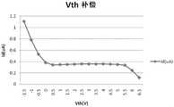
应用本申请实施例提供的像素驱动电路和像素驱动方法,对Vth的补偿效果如图5所示,图5的横坐标表示驱动晶体管T1的阈值电压Vth(单位V,即伏特),纵坐标表示驱动电流Id(单位为μA,即微安)。由图5可以看出,本申请实施例对Vth的补偿范围为0~5.5V,大于现有的像素驱动电路或像素补偿电路的补偿范围(通常为1V),本申请实施例通过OLED的驱动电流的波动ΔId<5%,相对于现有的像素驱动电路或像素补偿电路的补偿效果,有着显著优势。Applying the pixel driving circuit and pixel driving method provided by the embodiments of the present application, the compensation effect on Vth is shown in FIG. 5 . The abscissa of FIG. 5 represents the threshold voltage Vth (unit V, ie volt) of the driving transistor T1 , and the ordinate represents Drive current Id (unit is μA, that is, microampere). It can be seen from FIG. 5 that the compensation range for Vth in the embodiment of the present application is 0 to 5.5V, which is larger than the compensation range (usually 1V) of the existing pixel driving circuit or pixel compensation circuit. The embodiment of the present application uses the driving of the OLED The current fluctuation ΔId<5% has a significant advantage compared to the compensation effect of the existing pixel driving circuit or pixel compensation circuit.
应用本申请实施例提供的像素驱动电路和像素驱动方法,至少可以实现如下有益效果:By applying the pixel driving circuit and the pixel driving method provided by the embodiments of the present application, at least the following beneficial effects can be achieved:
1)采用本申请实施例提供的像素驱动电路和像素驱动方法,能够有效地对驱动晶体管的阈值电压Vth进行补偿,并具有较好的补偿效果,可降低阈值电压Vth的不稳定对显示亮度的影响,使显示亮度更加稳定、均一性更佳,从而改善显示画面的显示质量。1) By using the pixel driving circuit and the pixel driving method provided by the embodiments of the present application, the threshold voltage Vth of the driving transistor can be effectively compensated, and the compensation effect is good, and the instability of the threshold voltage Vth can reduce the influence on the display brightness. Influence, the display brightness is more stable and the uniformity is better, thereby improving the display quality of the display screen.
2)无需设计单独的基准电源信号,利用第一电压端的电源电压VDD即可对驱动晶体管的栅极进行复位,利用数据信号线Data输入的初始电压Vref即可对OLED的阳极进行复位,从而减少了驱动信号的数量,简化了复位流程。2) There is no need to design a separate reference power supply signal, the gate of the driving transistor can be reset by using the power supply voltage VDD of the first voltage terminal, and the anode of the OLED can be reset by using the initial voltage Vref input by the data signal line Data, thereby reducing The number of driving signals is reduced, and the reset process is simplified.
3)在本申请实施例提供的像素驱动电路工作时,只需要3条栅极驱动线(分别为扫描信号线Gate、第一控制信号线EM2和第二控制信号线EM1),信号波形简单,有利于实现显示装置的GOA(Gate on Array,栅极驱动电路阵列)设计。3) When the pixel driving circuit provided by the embodiment of the present application works, only 3 gate driving lines (respectively the scanning signal line Gate, the first control signal line EM2 and the second control signal line EM1 are required), and the signal waveform is simple, It is beneficial to realize the GOA (Gate on Array, gate drive circuit array) design of the display device.
基于同一发明构思,本申请实施例提供了一种显示装置,包括本申请实施例提供的像素驱动电路。Based on the same inventive concept, the embodiments of the present application provide a display device including the pixel driving circuit provided by the embodiments of the present application.
本申请实施例提供的显示装置,与前面所述的各实施例具有相同的发明构思及相同的有益效果,该显示装置中未详细示出的内容可参照前面所述的各实施例,在此不再赘述。The display device provided by the embodiments of the present application has the same inventive concept and the same beneficial effects as the aforementioned embodiments. For the content not shown in detail in the display device, reference may be made to the aforementioned embodiments. No longer.
本技术领域技术人员可以理解,本申请中已经讨论过的各种操作、方法、流程中的步骤、措施、方案可以被交替、更改、组合或删除。进一步地,具有本申请中已经讨论过的各种操作、方法、流程中的其他步骤、措施、方案也可以被交替、更改、重排、分解、组合或删除。进一步地,现有技术中的具有与本申请中公开的各种操作、方法、流程中的步骤、措施、方案也可以被交替、更改、重排、分解、组合或删除。Those skilled in the art can understand that various operations, methods, steps, measures, and solutions in the process discussed in this application may be alternated, modified, combined or deleted. Further, other steps, measures, and solutions in the various operations, methods, and processes that have been discussed in this application may also be alternated, modified, rearranged, decomposed, combined, or deleted. Further, steps, measures and solutions in the prior art with various operations, methods, and processes disclosed in this application may also be alternated, modified, rearranged, decomposed, combined or deleted.
术语“第一”、“第二”仅用于描述目的,而不能理解为指示或暗示相对重要性或者隐含指明所指示的技术特征的数量。由此,限定有“第一”、“第二”的特征可以明示或者隐含地包括一个或者更多个该特征。在本发明的描述中,除非另有说明,“多个”的含义是两个或两个以上。The terms "first" and "second" are only used for descriptive purposes, and should not be construed as indicating or implying relative importance or implicitly indicating the number of indicated technical features. Thus, a feature defined as "first", "second" may expressly or implicitly include one or more of that feature. In the description of the present invention, unless otherwise specified, "plurality" means two or more.
应该理解的是,虽然附图的流程图中的各个步骤按照箭头的指示依次显示,但是这些步骤并不是必然按照箭头指示的顺序依次执行。除非本文中有明确的说明,这些步骤的执行并没有严格的顺序限制,其可以以其他的顺序执行。而且,附图的流程图中的至少一部分步骤可以包括多个子步骤或者多个阶段,这些子步骤或者阶段并不必然是在同一时刻执行完成,而是可以在不同的时刻执行,其执行顺序也不必然是依次进行,而是可以与其他步骤或者其他步骤的子步骤或者阶段的至少一部分轮流或者交替地执行。It should be understood that although the various steps in the flowchart of the accompanying drawings are sequentially shown in the order indicated by the arrows, these steps are not necessarily executed in sequence in the order indicated by the arrows. Unless explicitly stated herein, the execution of these steps is not strictly limited to the order and may be performed in other orders. Moreover, at least a part of the steps in the flowchart of the accompanying drawings may include multiple sub-steps or multiple stages, and these sub-steps or stages are not necessarily executed at the same time, but may be executed at different times, and the execution sequence is also It does not have to be performed sequentially, but may be performed alternately or alternately with other steps or at least a portion of sub-steps or stages of other steps.
以上所述仅是本申请的部分实施方式,应当指出,对于本技术领域的普通技术人员来说,在不脱离本申请原理的前提下,还可以做出若干改进和润饰,这些改进和润饰也应视为本申请的保护范围。The above are only part of the embodiments of the present application. It should be pointed out that for those skilled in the art, without departing from the principles of the present application, several improvements and modifications can also be made. It should be regarded as the protection scope of this application.
Claims (10)
Priority Applications (2)
| Application Number | Priority Date | Filing Date | Title |
|---|---|---|---|
| CN201910243634.2ACN109754757B (en) | 2019-03-28 | 2019-03-28 | Pixel driving circuit, display device and pixel driving method |
| PCT/CN2020/077937WO2020192382A1 (en) | 2019-03-28 | 2020-03-05 | Pixel driving circuit, display device and pixel driving method |
Applications Claiming Priority (1)
| Application Number | Priority Date | Filing Date | Title |
|---|---|---|---|
| CN201910243634.2ACN109754757B (en) | 2019-03-28 | 2019-03-28 | Pixel driving circuit, display device and pixel driving method |
Publications (2)
| Publication Number | Publication Date |
|---|---|
| CN109754757A CN109754757A (en) | 2019-05-14 |
| CN109754757Btrue CN109754757B (en) | 2020-11-06 |
Family
ID=66409510
Family Applications (1)
| Application Number | Title | Priority Date | Filing Date |
|---|---|---|---|
| CN201910243634.2AActiveCN109754757B (en) | 2019-03-28 | 2019-03-28 | Pixel driving circuit, display device and pixel driving method |
Country Status (2)
| Country | Link |
|---|---|
| CN (1) | CN109754757B (en) |
| WO (1) | WO2020192382A1 (en) |
Cited By (1)
| Publication number | Priority date | Publication date | Assignee | Title |
|---|---|---|---|---|
| US12170060B2 (en) | 2021-06-25 | 2024-12-17 | Beijing Boe Technology Development Co., Ltd. | Pixel driving circuit, driving method for the pixel driving circuit, and display panel |
Families Citing this family (11)
| Publication number | Priority date | Publication date | Assignee | Title |
|---|---|---|---|---|
| CN109754757B (en)* | 2019-03-28 | 2020-11-06 | 京东方科技集团股份有限公司 | Pixel driving circuit, display device and pixel driving method |
| CN110444167A (en)* | 2019-06-28 | 2019-11-12 | 福建华佳彩有限公司 | A kind of AMOLED compensation circuit |
| CN110472606B (en) | 2019-08-21 | 2022-05-20 | 京东方科技集团股份有限公司 | An ultrasonic identification module, its driving method and display device |
| CN110544458B (en)* | 2019-09-10 | 2021-08-06 | 京东方科技集团股份有限公司 | A pixel circuit, a driving method thereof, and a display device |
| TWI708233B (en)* | 2019-09-20 | 2020-10-21 | 友達光電股份有限公司 | Pixel circuit for low frame rate and display device having the same |
| KR102811546B1 (en)* | 2019-12-30 | 2025-05-21 | 엘지디스플레이 주식회사 | Pixel circuit and light emitting display device and driving method for the same |
| CN114822427B (en)* | 2021-01-28 | 2025-06-10 | 成都九天画芯科技有限公司 | Control circuit and control method for liquid crystal pixel |
| CN113920923B (en)* | 2021-10-18 | 2022-09-09 | 深圳市华星光电半导体显示技术有限公司 | Light emitting device driving circuit, backlight module and display panel |
| CN115731872A (en)* | 2022-11-23 | 2023-03-03 | 京东方科技集团股份有限公司 | Display substrate, driving method of pixel driving circuit and display device |
| CN115881029A (en)* | 2022-12-27 | 2023-03-31 | 深圳市华星光电半导体显示技术有限公司 | Pixel driving circuit, driving method thereof and display panel |
| CN117037715A (en)* | 2023-08-01 | 2023-11-10 | 云谷(固安)科技有限公司 | Pixel circuit, display panel and light emission control method |
Family Cites Families (13)
| Publication number | Priority date | Publication date | Assignee | Title |
|---|---|---|---|---|
| KR20160055546A (en)* | 2014-11-10 | 2016-05-18 | 삼성디스플레이 주식회사 | Organic light emitting diode display |
| CN104409043B (en)* | 2014-12-05 | 2016-08-24 | 京东方科技集团股份有限公司 | Pixel-driving circuit and image element driving method, display device |
| KR102285390B1 (en)* | 2015-01-28 | 2021-08-04 | 삼성디스플레이 주식회사 | Organic light emitting display apparatus |
| CN104809989A (en)* | 2015-05-22 | 2015-07-29 | 京东方科技集团股份有限公司 | Pixel circuit, drive method thereof and related device |
| CN106887207A (en)* | 2015-12-15 | 2017-06-23 | 昆山工研院新型平板显示技术中心有限公司 | Image element circuit and its driving method and OLED |
| CN106023900A (en)* | 2016-08-01 | 2016-10-12 | 上海天马有机发光显示技术有限公司 | Organic light-emitting display panel and driving method thereof |
| CN106652912B (en)* | 2016-12-13 | 2020-05-19 | 上海天马有机发光显示技术有限公司 | Organic light-emitting pixel driving circuit, driving method and organic light-emitting display panel |
| CN109215569B (en)* | 2017-07-04 | 2020-12-25 | 京东方科技集团股份有限公司 | Pixel circuit, driving method and display device |
| CN107230451B (en)* | 2017-07-11 | 2018-01-16 | 深圳市华星光电半导体显示技术有限公司 | A kind of AMOLED pixel-driving circuits and image element driving method |
| KR102348669B1 (en)* | 2017-07-20 | 2022-01-06 | 엘지디스플레이 주식회사 | Organic light emitting display device and method for driving the same |
| CN107221289B (en)* | 2017-08-02 | 2019-09-27 | 上海天马有机发光显示技术有限公司 | A kind of pixel-driving circuit and its control method and display panel, display device |
| CN109064975B (en)* | 2018-09-28 | 2020-04-03 | 昆山国显光电有限公司 | Pixel circuit, driving method thereof, display panel and display device |
| CN109754757B (en)* | 2019-03-28 | 2020-11-06 | 京东方科技集团股份有限公司 | Pixel driving circuit, display device and pixel driving method |
- 2019
- 2019-03-28CNCN201910243634.2Apatent/CN109754757B/enactiveActive
- 2020
- 2020-03-05WOPCT/CN2020/077937patent/WO2020192382A1/ennot_activeCeased
Cited By (1)
| Publication number | Priority date | Publication date | Assignee | Title |
|---|---|---|---|---|
| US12170060B2 (en) | 2021-06-25 | 2024-12-17 | Beijing Boe Technology Development Co., Ltd. | Pixel driving circuit, driving method for the pixel driving circuit, and display panel |
Also Published As
| Publication number | Publication date |
|---|---|
| CN109754757A (en) | 2019-05-14 |
| WO2020192382A1 (en) | 2020-10-01 |
Similar Documents
| Publication | Publication Date | Title |
|---|---|---|
| CN109754757B (en) | Pixel driving circuit, display device and pixel driving method | |
| CN109493795B (en) | Pixel circuit, pixel driving method and display device | |
| CN106558287B (en) | Organic light-emitting pixel driving circuit, driving method and organic light-emitting display panel | |
| CN103778889B (en) | Organic light emitting diode circuit and driving method thereof | |
| CN109493794B (en) | Pixel circuit, pixel driving method and display device | |
| CN108648696B (en) | Pixel circuit, array substrate, display device, and pixel driving method | |
| CN103165080B (en) | Pixel circuit and driving method and display device thereof | |
| US20210358390A1 (en) | Subpixel circuit, pixel circuit, driving method thereof, display module and display device | |
| CN103927981B (en) | Image element circuit and driving method thereof, display unit | |
| CN103927982B (en) | Image element circuit and driving method, display device | |
| CN110062943B (en) | Pixel circuit, driving method thereof and display device | |
| CN104485074B (en) | Pixel-driving circuit, method and display device | |
| CN109509433A (en) | Pixel circuit, display device and image element driving method | |
| CN112233621B (en) | A pixel drive circuit, a display panel and an electronic device | |
| CN111341267B (en) | Pixel circuit and driving method thereof | |
| CN105427805A (en) | Pixel driving circuit and method, display panel, and display apparatus | |
| WO2020192278A1 (en) | Pixel circuit and driving method therefor, and display substrate and display device | |
| CN108172171B (en) | Pixel driving circuit and organic light emitting diode display | |
| CN106952618A (en) | Display device, pixel circuit and control method thereof | |
| CN106991976A (en) | Image element circuit, image element driving method and display device | |
| WO2022226727A1 (en) | Pixel circuit, pixel driving method and display device | |
| CN107507566B (en) | Pixel-driving circuit, display device and driving method | |
| CN110517639A (en) | Pixel compensation circuit, pixel circuit, display device and pixel compensation method | |
| CN114694572B (en) | Driving circuit, display device and electronic equipment | |
| CN108847183B (en) | Pixel driving circuit and display panel |
Legal Events
| Date | Code | Title | Description |
|---|---|---|---|
| PB01 | Publication | ||
| PB01 | Publication | ||
| SE01 | Entry into force of request for substantive examination | ||
| SE01 | Entry into force of request for substantive examination | ||
| GR01 | Patent grant | ||
| GR01 | Patent grant |