CN109727900B - Substrate transfer robot end effector - Google Patents
Substrate transfer robot end effectorDownload PDFInfo
- Publication number
- CN109727900B CN109727900BCN201811152281.7ACN201811152281ACN109727900BCN 109727900 BCN109727900 BCN 109727900BCN 201811152281 ACN201811152281 ACN 201811152281ACN 109727900 BCN109727900 BCN 109727900B
- Authority
- CN
- China
- Prior art keywords
- substrate
- contact surface
- support member
- contact
- angle
- Prior art date
- Legal status (The legal status is an assumption and is not a legal conclusion. Google has not performed a legal analysis and makes no representation as to the accuracy of the status listed.)
- Active
Links
Images


Classifications
- H—ELECTRICITY
- H01—ELECTRIC ELEMENTS
- H01L—SEMICONDUCTOR DEVICES NOT COVERED BY CLASS H10
- H01L21/00—Processes or apparatus adapted for the manufacture or treatment of semiconductor or solid state devices or of parts thereof
- H01L21/67—Apparatus specially adapted for handling semiconductor or electric solid state devices during manufacture or treatment thereof; Apparatus specially adapted for handling wafers during manufacture or treatment of semiconductor or electric solid state devices or components ; Apparatus not specifically provided for elsewhere
- H01L21/677—Apparatus specially adapted for handling semiconductor or electric solid state devices during manufacture or treatment thereof; Apparatus specially adapted for handling wafers during manufacture or treatment of semiconductor or electric solid state devices or components ; Apparatus not specifically provided for elsewhere for conveying, e.g. between different workstations
- H01L21/67739—Apparatus specially adapted for handling semiconductor or electric solid state devices during manufacture or treatment thereof; Apparatus specially adapted for handling wafers during manufacture or treatment of semiconductor or electric solid state devices or components ; Apparatus not specifically provided for elsewhere for conveying, e.g. between different workstations into and out of processing chamber
- H01L21/67742—Mechanical parts of transfer devices
- H—ELECTRICITY
- H01—ELECTRIC ELEMENTS
- H01L—SEMICONDUCTOR DEVICES NOT COVERED BY CLASS H10
- H01L21/00—Processes or apparatus adapted for the manufacture or treatment of semiconductor or solid state devices or of parts thereof
- H01L21/67—Apparatus specially adapted for handling semiconductor or electric solid state devices during manufacture or treatment thereof; Apparatus specially adapted for handling wafers during manufacture or treatment of semiconductor or electric solid state devices or components ; Apparatus not specifically provided for elsewhere
- H01L21/677—Apparatus specially adapted for handling semiconductor or electric solid state devices during manufacture or treatment thereof; Apparatus specially adapted for handling wafers during manufacture or treatment of semiconductor or electric solid state devices or components ; Apparatus not specifically provided for elsewhere for conveying, e.g. between different workstations
- H01L21/67763—Apparatus specially adapted for handling semiconductor or electric solid state devices during manufacture or treatment thereof; Apparatus specially adapted for handling wafers during manufacture or treatment of semiconductor or electric solid state devices or components ; Apparatus not specifically provided for elsewhere for conveying, e.g. between different workstations the wafers being stored in a carrier, involving loading and unloading
- H01L21/67766—Mechanical parts of transfer devices
- H—ELECTRICITY
- H01—ELECTRIC ELEMENTS
- H01L—SEMICONDUCTOR DEVICES NOT COVERED BY CLASS H10
- H01L21/00—Processes or apparatus adapted for the manufacture or treatment of semiconductor or solid state devices or of parts thereof
- H01L21/67—Apparatus specially adapted for handling semiconductor or electric solid state devices during manufacture or treatment thereof; Apparatus specially adapted for handling wafers during manufacture or treatment of semiconductor or electric solid state devices or components ; Apparatus not specifically provided for elsewhere
- H01L21/677—Apparatus specially adapted for handling semiconductor or electric solid state devices during manufacture or treatment thereof; Apparatus specially adapted for handling wafers during manufacture or treatment of semiconductor or electric solid state devices or components ; Apparatus not specifically provided for elsewhere for conveying, e.g. between different workstations
- H01L21/67784—Apparatus specially adapted for handling semiconductor or electric solid state devices during manufacture or treatment thereof; Apparatus specially adapted for handling wafers during manufacture or treatment of semiconductor or electric solid state devices or components ; Apparatus not specifically provided for elsewhere for conveying, e.g. between different workstations using air tracks
- H01L21/67787—Apparatus specially adapted for handling semiconductor or electric solid state devices during manufacture or treatment thereof; Apparatus specially adapted for handling wafers during manufacture or treatment of semiconductor or electric solid state devices or components ; Apparatus not specifically provided for elsewhere for conveying, e.g. between different workstations using air tracks with angular orientation of the workpieces
- H—ELECTRICITY
- H01—ELECTRIC ELEMENTS
- H01L—SEMICONDUCTOR DEVICES NOT COVERED BY CLASS H10
- H01L21/00—Processes or apparatus adapted for the manufacture or treatment of semiconductor or solid state devices or of parts thereof
- H01L21/67—Apparatus specially adapted for handling semiconductor or electric solid state devices during manufacture or treatment thereof; Apparatus specially adapted for handling wafers during manufacture or treatment of semiconductor or electric solid state devices or components ; Apparatus not specifically provided for elsewhere
- H01L21/677—Apparatus specially adapted for handling semiconductor or electric solid state devices during manufacture or treatment thereof; Apparatus specially adapted for handling wafers during manufacture or treatment of semiconductor or electric solid state devices or components ; Apparatus not specifically provided for elsewhere for conveying, e.g. between different workstations
- H01L21/67796—Apparatus specially adapted for handling semiconductor or electric solid state devices during manufacture or treatment thereof; Apparatus specially adapted for handling wafers during manufacture or treatment of semiconductor or electric solid state devices or components ; Apparatus not specifically provided for elsewhere for conveying, e.g. between different workstations with angular orientation of workpieces
- H—ELECTRICITY
- H01—ELECTRIC ELEMENTS
- H01L—SEMICONDUCTOR DEVICES NOT COVERED BY CLASS H10
- H01L21/00—Processes or apparatus adapted for the manufacture or treatment of semiconductor or solid state devices or of parts thereof
- H01L21/67—Apparatus specially adapted for handling semiconductor or electric solid state devices during manufacture or treatment thereof; Apparatus specially adapted for handling wafers during manufacture or treatment of semiconductor or electric solid state devices or components ; Apparatus not specifically provided for elsewhere
- H01L21/683—Apparatus specially adapted for handling semiconductor or electric solid state devices during manufacture or treatment thereof; Apparatus specially adapted for handling wafers during manufacture or treatment of semiconductor or electric solid state devices or components ; Apparatus not specifically provided for elsewhere for supporting or gripping
- H01L21/6835—Apparatus specially adapted for handling semiconductor or electric solid state devices during manufacture or treatment thereof; Apparatus specially adapted for handling wafers during manufacture or treatment of semiconductor or electric solid state devices or components ; Apparatus not specifically provided for elsewhere for supporting or gripping using temporarily an auxiliary support
- H—ELECTRICITY
- H01—ELECTRIC ELEMENTS
- H01L—SEMICONDUCTOR DEVICES NOT COVERED BY CLASS H10
- H01L21/00—Processes or apparatus adapted for the manufacture or treatment of semiconductor or solid state devices or of parts thereof
- H01L21/67—Apparatus specially adapted for handling semiconductor or electric solid state devices during manufacture or treatment thereof; Apparatus specially adapted for handling wafers during manufacture or treatment of semiconductor or electric solid state devices or components ; Apparatus not specifically provided for elsewhere
- H01L21/683—Apparatus specially adapted for handling semiconductor or electric solid state devices during manufacture or treatment thereof; Apparatus specially adapted for handling wafers during manufacture or treatment of semiconductor or electric solid state devices or components ; Apparatus not specifically provided for elsewhere for supporting or gripping
- H01L21/687—Apparatus specially adapted for handling semiconductor or electric solid state devices during manufacture or treatment thereof; Apparatus specially adapted for handling wafers during manufacture or treatment of semiconductor or electric solid state devices or components ; Apparatus not specifically provided for elsewhere for supporting or gripping using mechanical means, e.g. chucks, clamps or pinches
- H01L21/68707—Apparatus specially adapted for handling semiconductor or electric solid state devices during manufacture or treatment thereof; Apparatus specially adapted for handling wafers during manufacture or treatment of semiconductor or electric solid state devices or components ; Apparatus not specifically provided for elsewhere for supporting or gripping using mechanical means, e.g. chucks, clamps or pinches the wafers being placed on a robot blade, or gripped by a gripper for conveyance
Landscapes
- Engineering & Computer Science (AREA)
- Physics & Mathematics (AREA)
- Condensed Matter Physics & Semiconductors (AREA)
- General Physics & Mathematics (AREA)
- Manufacturing & Machinery (AREA)
- Computer Hardware Design (AREA)
- Microelectronics & Electronic Packaging (AREA)
- Power Engineering (AREA)
- Robotics (AREA)
- Container, Conveyance, Adherence, Positioning, Of Wafer (AREA)
- Manipulator (AREA)
Abstract
Translated fromChinese
Description
Translated fromChinese本申请是申请日为2015年6月5日、申请号为201580036350.6、发明名称为“基板传送机械手终端受动器”的发明专利申请的分案申请。This application is a divisional application of an invention patent application with an application date of June 5, 2015, an application number of 201580036350.6, and an invention title of "substrate transfer manipulator terminal effector".
技术领域technical field
本公开内容的实施方式总体涉及半导体处理设备。Embodiments of the present disclosure generally relate to semiconductor processing equipment.
背景技术Background technique
在半导体基板上的微电子器件的制造中,在制造工艺期间多次于基板边缘及背侧上处置(handle)半导体基板。该处置可引起污染物粘着于基板背侧且于处理部件之间移动,例如,循着基板、或于不同基板之间由腔室至腔室、FOUP(前开式晶片传送盒)至FOUP、或处理工具至处理工具,非期望地增加用于保养的工具停机时间,以用于移除污染物。这些污染物也可转移至基板前侧,而导致降低的设备性能和/或良率损失。In the fabrication of microelectronic devices on semiconductor substrates, the semiconductor substrate is handled on the edge and backside of the substrate several times during the fabrication process. This handling can cause contaminants to stick to the backside of the substrate and move between processing components, for example, along the substrate, or between different substrates from chamber to chamber, FOUP (front opening wafer transfer pod) to FOUP, Or process tool to process tool, undesirably increasing tool downtime for maintenance to remove contaminants. These contaminants can also be transferred to the substrate front side, resulting in reduced device performance and/or yield loss.
上述问题的典型解法意图通过减少到基板与基板传送/处置器件之间的接触面积来降低背侧颗粒的产生。然而,减小接触面积可减轻颗粒产生的同时,发明人观察到:即便使用最小的考量的接触面积,仍旧产生大量的颗粒。Typical solutions to the above problems aim to reduce the generation of backside particles by reducing the contact area between the substrate and the substrate transfer/handling device. However, while reducing the contact area reduces particle generation, the inventors have observed that even with the smallest considered contact area, a large number of particles are still generated.
因此,发明人提供具有减少的颗粒产生的用于支撑及处置基板的改良装置的实施方式。Accordingly, the inventors provide embodiments of improved apparatus for supporting and handling substrates with reduced particle generation.
发明内容Contents of the invention
于此公开用于支撑基板的装置的实施方式。在一些实施方式中,用于支撑基板的装置包含:支撑构件;及多个基板接触元件,该多个基板接触元件由该支撑构件突出,其中该多个基板接触元件的每一个包含:第一接触表面,在基板放置于该第一接触表面上时支撑该基板;及第二接触表面,该第二接触表面由该第一接触表面延伸;其中该第二接触表面邻近该基板的周边以防止该基板的径向移动;其中该第一接触表面相关于该支撑构件处于第一角度,且该第二接触表面相关于该支撑构件处于第二角度;并且其中该第一角度介于约3度及5度之间。Embodiments of an apparatus for supporting a substrate are disclosed herein. In some embodiments, an apparatus for supporting a substrate comprises: a support member; and a plurality of substrate contact elements protruding from the support member, wherein each of the plurality of substrate contact elements comprises: a first a contact surface that supports the substrate when it is placed on the first contact surface; and a second contact surface that extends from the first contact surface; wherein the second contact surface is adjacent to the periphery of the substrate to prevent radial movement of the substrate; wherein the first contact surface is at a first angle relative to the support member, and the second contact surface is at a second angle relative to the support member; and wherein the first angle is between about 3 degrees and 5 degrees.
在一些实施方式中,用于传送基板的基板传送机械手包含:臂,该臂包含叶片;及多个基板接触元件,该多个基板接触元件由该叶片的上表面突出。该多个基板接触元件的每一个包含:第一接触表面,在基板放置于该第一接触表面上时支撑该基板;及第二接触表面,该第二接触表面由该第一接触表面延伸;其中该第二接触表面邻近该基板的周边以防止该基板的径向移动;其中该第一接触表面相关于该上表面处于第一角度,且该第二接触表面相关于该上表面处于第二角度;并且其中该第一角度介于约3度与5度之间。In some embodiments, a substrate transfer robot for transferring a substrate includes: an arm including a blade; and a plurality of substrate contact elements protruding from an upper surface of the blade. Each of the plurality of substrate contact elements includes: a first contact surface supporting the substrate when placed on the first contact surface; and a second contact surface extending from the first contact surface; wherein the second contact surface is adjacent to the periphery of the substrate to prevent radial movement of the substrate; wherein the first contact surface is at a first angle relative to the upper surface, and the second contact surface is at a second angle relative to the upper surface angle; and wherein the first angle is between about 3 degrees and 5 degrees.
在一些实施方式中,用于传送基板的基板传送机械手包含:臂,该臂包含叶片,其中该叶片由电性传导掺钛陶瓷形成;及多个基板接触元件,该多个基板接触元件由该叶片的上表面突出。该多个基板接触元件的每一个包含:第一接触表面,在基板放置于该第一接触表面上时支撑该基板;及第二接触表面,该第二接触表面由该第一接触表面延伸;其中该第二接触表面邻近该基板的周边以防止该基板的径向移动;其中该第一接触表面相关于该上表面处于第一角度,且该第二接触表面相对于该上表面处于第二角度,其中该第一角度介于约3度与5度之间,并且其中该第二角度大于该第一角度。In some embodiments, a substrate transfer robot for transferring a substrate includes: an arm including a blade, wherein the blade is formed from an electrically conductive titanium-doped ceramic; and a plurality of substrate contact elements formed from the The upper surface of the blade is prominent. Each of the plurality of substrate contact elements includes: a first contact surface supporting the substrate when placed on the first contact surface; and a second contact surface extending from the first contact surface; wherein the second contact surface is adjacent to the periphery of the substrate to prevent radial movement of the substrate; wherein the first contact surface is at a first angle relative to the upper surface, and the second contact surface is at a second angle relative to the upper surface angle, wherein the first angle is between about 3 degrees and 5 degrees, and wherein the second angle is greater than the first angle.
以下描述本公开内容的其它的及进一步的实施方式。Other and further embodiments of the present disclosure are described below.
附图说明Description of drawings
以上简要概述、及以下将更详细讨论的本公开内容的实施方式可通过参照描绘于附图中的本公开内容的说明性实施方式而理解。然而,附图仅绘示本公开内容的典型的实施方式,因而不应视为对范围的限制,因为本公开内容可允许其它等同有效实施方式。Embodiments of the disclosure, briefly summarized above, and discussed in greater detail below, can be understood by reference to the illustrative embodiments of the disclosure depicted in the accompanying drawings. The drawings, however, depict only typical implementations of this disclosure and are therefore not to be considered limiting of scope, for the disclosure may admit to other equally effective embodiments.
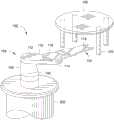
图1根据本公开内容的一些实施方式描绘用于传送基板的基板传送机械手的示意图,该基板安置于基板支撑件的升降销上。1 depicts a schematic diagram of a substrate transfer robot for transferring a substrate seated on lift pins of a substrate support, according to some embodiments of the present disclosure.
图2根据本公开内容的一些实施方式描绘基板传送机械手的终端受动器的等距图。2 depicts an isometric view of an end effector of a substrate transfer robot, according to some embodiments of the present disclosure.
图3根据本公开内容的一些实施方式描绘基板传送机械手叶片的部分的侧截面图。3 depicts a side cross-sectional view of a portion of a substrate transfer robot blade, according to some embodiments of the present disclosure.
图4根据本公开内容的一些实施方式描绘基板传送机械手叶片的部分的侧截面图。4 depicts a side cross-sectional view of a portion of a substrate transfer robot blade, according to some embodiments of the present disclosure.
图5根据本公开内容的一些实施方式描绘基板传送机械手的终端受动器的平面图。5 depicts a plan view of an end effector of a substrate transfer robot, according to some embodiments of the present disclosure.
图6根据本公开内容的一些实施方式描绘基板传送机械手叶片的部分的侧截面图。6 depicts a side cross-sectional view of a portion of a substrate transfer robot blade, according to some embodiments of the present disclosure.
为了便于理解,尽可能地使用相同附图标号,以标示附图中共通的相同元件。附图并未按比例绘制且可为了清晰而简化。一个实施方式中的元件及特征在没有进一步地描述下可有益地并入于其它实施方式。In order to facilitate understanding, the same reference numerals are used as much as possible to designate the same elements common to the drawings. The figures are not drawn to scale and may be simplified for clarity. Elements and features of one embodiment may be beneficially incorporated in other embodiments without further description.
具体实施方式Detailed ways
本公开内容的实施方式提供改良的基板处置装置,该基板处置装置提供相较于传统基板支撑装置而言降低的颗粒产生。本公开内容的实施方式可有优势地在制造工艺期间避免或减少累积于基板上的污染物,例如,在工艺步骤之间处置基板时,这样可进一步限制或防止污染物到达基板前侧且引起器件性能问题和/或良率损失。可使用本公开内容的实施方式于处理中接触基板的广泛多样的表面中,这些处理想要非常低的颗粒引入,例如,于显示处理、硅晶片处理、光学元件制造,诸如此类之中。Embodiments of the present disclosure provide an improved substrate handling apparatus that provides reduced particle generation compared to conventional substrate support apparatus. Embodiments of the present disclosure may advantageously avoid or reduce the accumulation of contaminants on the substrate during the manufacturing process, for example, when the substrate is handled between process steps, which may further limit or prevent contamination from reaching the front side of the substrate and causing Device performance issues and/or yield loss. Embodiments of the present disclosure may be used in a wide variety of surfaces that contact substrates in processes where very low particle incorporation is desired, for example, in display processing, silicon wafer processing, optical element fabrication, and the like.
图1根据本公开内容的一些实施方式描绘基板传送机械手100。例如,基板传送机械手100可包括在第一端106处用于垂直及旋转位移的机械臂(臂104)。臂104可包括一个或更多个联接(link),例如第一联接108及在轴112处钉在一起的第二联接110。臂104的第二端114可包含肘节116,叶片102的第一端耦接至肘节116。叶片102可包含由叶片的上表面突出的接触垫118以支撑基板。以下相关于图2至图6更详细描述接触垫118。FIG. 1 depicts a
在操作中,可控制基板传送机械手100使得叶片102被放置于基板150下方,于多个升降销120上支撑基板150。经由基板传送机械手100及臂104的操纵,叶片102由基板150下方的位置升起,从而使接触垫118与基板150的边缘或背侧中的至少一者接触,及升高基板150离开升降销120。在接触基板150时,通常在接触垫118与基板150之间的接触面积处产生颗粒。In operation, the
发明人发现:当接触基板的任何元件材料较基板材料(例如硅)硬时,产生的颗粒具有对于基板材料的高粘着性,无法防止基板滑动,具有粗糙表面、及非传导性。例如,若初始由粘性材料形成的元件接触基板,并且随后通过由硬材料形成的另一元件接触基板,将恶化基板上颗粒的产生。相似地,若有电流于基板及传导性材料之间流动并且基板由非传导性材料升高,可发生电弧而恶化基板上颗粒的产生。The inventors found that when any component material contacting the substrate is harder than the substrate material (such as silicon), the resulting particles have high adhesion to the substrate material, cannot prevent the substrate from sliding, have a rough surface, and are non-conductive. For example, particle generation on the substrate will be exacerbated if an element initially formed of a viscous material contacts the substrate and is subsequently contacted by another element formed of a hard material. Similarly, if there is current flowing between the substrate and the conductive material and the substrate is lifted by the non-conductive material, arcing can occur and worsen particle generation on the substrate.
发明人发现:可通过使用一材料防止或实质上最小化颗粒的产生,该材料展现出接触基板的元件(例如,接触垫118)中的一组预先确定的性能。该组预先确定的性能包含:小于或等于欲支撑基板的硬度的硬度(例如,硅)、非粘着性、高至足以防止基板于接触基板的元件上滑动的静磨擦系数、电性传导性、及小于或等于10Ra的表面粗糙度。该材料可包含:例如,氧化铝、氮化硅、不锈钢、及电性传导性塑料之中的一或多种,电性传导性塑料诸如


传统边缘接触垫包含相关于水平面处于一陡峭的角度(接近60度)的边缘支撑表面。发明人发现:在升高基板后,由于边缘支撑表面角度的陡峭度,基板滑入最终安置位置,造成基板边缘上的颗粒产生。因此,发明人发现:可通过提供边缘接触垫一小角度斜面以防止或实质上最小化颗粒的产生。Conventional edge contact pads include edge support surfaces at a steep angle (approximately 60 degrees) with respect to the horizontal. The inventors have found that after raising the substrate, due to the steepness of the edge support surface angle, the substrate slides into the final seating position, causing particle generation on the edge of the substrate. Accordingly, the inventors have discovered that particle generation can be prevented or substantially minimized by providing edge contact pads with a small angled bevel.
例如,图2根据本公开内容的一些实施方式描绘终端受动器202。终端受动器202包含耦接至支撑构件204的多个边缘接触垫210(图2示出四个)。可以如图1所描绘的接触垫118那样使用边缘接触垫210。在一些实施方式中,支撑构件204为实质平面的,或包含足以支撑基板的实质平面区域。在一些实施方式中,支撑构件204由陶瓷材料形成且可使用钛来掺杂。掺钛陶瓷材料相较于传统基板传送机械手叶片而言,对于下垂有利地提供更多阻力。此外,掺钛陶瓷支撑构件有利地为电性传导性。终端受动器202也可包含特征结构206,例如孔,特征结构206可用于基板对齐的目的和/或终端受动器202的重量减轻。前及后边缘接触垫210之间的距离L较被处理的基板的直径稍大。例如,对于处置具有300mm直径的基板,距离L可为约304mm。然而,距离L将依据被处置基板的大小而定。For example, Figure 2 depicts an
图3根据本公开内容的一些实施方式描绘边缘接触垫210的侧视图。边缘接触垫210包含第一接触表面302及第二接触表面304。第一接触表面302相关于支撑构件204具有第一角度θ。第二接触表面304相关于支撑构件204具有第二角度α。由于基板150的重量及由基板传送机械手100所造成的基板150移动的惯性力,各个边缘接触垫210给予基板上的垂直(摩擦)力及径向力。径向力被引导朝向基板150中央以确保基板150保持静止。为了确保基板上足够强度的摩擦及径向力,第一角度θ可介于约3度及5度之间。第一角度θ足够小以确保存在经引导朝向基板中央的径向力,同时保持足够的摩擦力以防止基板滑动。第一接触表面302的水平长度可介于约4mm至约7mm之间,优选约5.8mm。第二角度α较第一角度θ大,使得第二接触表面304实质垂直。第二接触表面304充当缓冲器以免放置期间基板滑动。FIG. 3 depicts a side view of
边缘接触垫210耦接至终端受动器202的支撑构件204。在一些实施方式中,可使用一个或更多个螺钉306以耦接边缘接触垫210至支撑构件204。螺钉306包含通孔,以确保抽空螺钉306及边缘接触垫210之间的任何空气袋。在一些实施方式中,可使用一个或更多个垫片308以控制支撑构件204上方的边缘接触垫210的高度,因此有利地确保基板于所有边缘接触垫上恰当地水平。The
图4根据本公开内容的一些实施方式描绘边缘接触垫210的透视图。图4中所描绘的边缘接触垫210与图3中所示出的边缘接触垫210相似,除了图4中的边缘接触垫210包含弯曲的第一接触表面402及第二接触表面404(相较于图3中所示的线性表面)。发明人发现:通过提供弯曲的接触表面,施加至基板的摩擦及径向力依基板位置而改变。如此,若基板滑动,作用于基板上的径向力随相关于边缘接触垫210的基板位置而增加或减少。例如,径向力在基板处于较高角度时更高而在基板处于较低角度时更低。结果,限制或防止了特定方向上基板的进一步滑动。第一及第二接触表面402、404及水平平面之间的角度θ在第一接触表面402的起始处由0度或接近0度改变至在第二接触表面404的末端处的90度或接近90度。第一接触表面402(例如,更小角度处且更径向朝内的弯曲表面部分)起到对于放置于第一接触表面402上的基板的支撑表面的作用,并且第二接触表面404(例如,更大角度处且更径向朝外的弯曲表面部分)起到缓冲器的作用以防止基板滑动。第一及第二接触表面402、404形成一连续弯曲表面。或者,可使用弯曲及线性表面的组合而提供更小角度的角度以支撑基板及更大角度以防止若打滑时基板进一步的移动。FIG. 4 depicts a perspective view of an
图5根据本公开内容的一些实施方式描绘终端受动器500。终端受动器500包含耦接至终端受动器500的支撑构件502的背侧接触垫510,以由基板背侧支撑基板,而非如以上相关于图2至图4所描述的边缘。可如图1中所描绘的接触垫118那样使用背侧接触垫510。当基板传送机械手升高基板150离开升降销120时,基板150由速度零加速到传送速度。该加速导致对应于接触垫118的位置的接触区域的力F,如图6中所图示。结果,背侧接触垫510及基板150之间的接触面积处产生颗粒。FIG. 5 depicts an
相似于边缘接触垫210,可使用螺钉506将背侧接触垫510耦接至终端受动器500的支撑构件502。可排出螺钉506从而排出螺钉及背侧接触垫510之间的任何空气空隙。虽然未示出,可使用相似于图3及图4中所描绘的这些垫片以升高任何背侧接触垫510,以在基板150放置于背侧接触垫510上时确保基板150合适的平整。Similar to edge
因此,于此公开用于避免于基板上产生颗粒的改良的装置及材料。在制造工艺期间,例如,在工艺步骤之间的处置基板期间及在处理腔室内部支撑基板时,发明的装置可有利地使累积于基板上的污染物减少或防止污染物累积于基板上,因而防止或降低污染物的发生率而免于达到基板前侧和引发降低的装置效率和/或良率损失。Accordingly, improved devices and materials for avoiding particle generation on substrates are disclosed herein. The inventive apparatus advantageously reduces or prevents the accumulation of contaminants on the substrate during the manufacturing process, for example, during handling of the substrate between process steps and while supporting the substrate inside a processing chamber, Thus preventing or reducing the incidence of contamination from reaching the substrate front side and causing reduced device efficiency and/or yield loss.
尽管前述针对本公开内容的实施方式,但在不脱离本公开内容的基本范围的条件下可设计本公开内容的其它的及进一步的实施方式。While the foregoing is directed to embodiments of the present disclosure, other and further embodiments of the present disclosure can be devised without departing from the essential scope of the present disclosure.
Claims (9)
Priority Applications (1)
| Application Number | Priority Date | Filing Date | Title |
|---|---|---|---|
| CN201811152281.7ACN109727900B (en) | 2014-07-03 | 2015-06-05 | Substrate transfer robot end effector |
Applications Claiming Priority (7)
| Application Number | Priority Date | Filing Date | Title |
|---|---|---|---|
| US201462020769P | 2014-07-03 | 2014-07-03 | |
| US62/020,769 | 2014-07-03 | ||
| US14/476,224US9425076B2 (en) | 2014-07-03 | 2014-09-03 | Substrate transfer robot end effector |
| US14/476,224 | 2014-09-03 | ||
| CN201811152281.7ACN109727900B (en) | 2014-07-03 | 2015-06-05 | Substrate transfer robot end effector |
| PCT/US2015/034333WO2016003598A1 (en) | 2014-07-03 | 2015-06-05 | Substrate transfer robot end effector |
| CN201580036350.6ACN106489194B (en) | 2014-07-03 | 2015-06-05 | Substrate transfer robot end effector |
Related Parent Applications (1)
| Application Number | Title | Priority Date | Filing Date |
|---|---|---|---|
| CN201580036350.6ADivisionCN106489194B (en) | 2014-07-03 | 2015-06-05 | Substrate transfer robot end effector |
Publications (2)
| Publication Number | Publication Date |
|---|---|
| CN109727900A CN109727900A (en) | 2019-05-07 |
| CN109727900Btrue CN109727900B (en) | 2023-05-09 |
Family
ID=55017516
Family Applications (2)
| Application Number | Title | Priority Date | Filing Date |
|---|---|---|---|
| CN201580036350.6AActiveCN106489194B (en) | 2014-07-03 | 2015-06-05 | Substrate transfer robot end effector |
| CN201811152281.7AActiveCN109727900B (en) | 2014-07-03 | 2015-06-05 | Substrate transfer robot end effector |
Family Applications Before (1)
| Application Number | Title | Priority Date | Filing Date |
|---|---|---|---|
| CN201580036350.6AActiveCN106489194B (en) | 2014-07-03 | 2015-06-05 | Substrate transfer robot end effector |
Country Status (9)
| Country | Link |
|---|---|
| US (1) | US9425076B2 (en) |
| EP (1) | EP3164883A4 (en) |
| JP (2) | JP2017522738A (en) |
| KR (1) | KR102509442B1 (en) |
| CN (2) | CN106489194B (en) |
| IL (1) | IL249505A0 (en) |
| SG (1) | SG11201610314UA (en) |
| TW (1) | TWI628738B (en) |
| WO (1) | WO2016003598A1 (en) |
Families Citing this family (15)
| Publication number | Priority date | Publication date | Assignee | Title |
|---|---|---|---|---|
| US10312127B2 (en) | 2013-09-16 | 2019-06-04 | Applied Materials, Inc. | Compliant robot blade for defect reduction |
| US9536329B2 (en)* | 2014-05-30 | 2017-01-03 | Adobe Systems Incorporated | Method and apparatus for performing sentiment analysis based on user reactions to displayable content |
| JP6276317B2 (en)* | 2016-03-31 | 2018-02-07 | 平田機工株式会社 | Hand unit and transfer method |
| US10090188B2 (en)* | 2016-05-05 | 2018-10-02 | Applied Materials, Inc. | Robot subassemblies, end effector assemblies, and methods with reduced cracking |
| JP6757646B2 (en)* | 2016-10-27 | 2020-09-23 | 川崎重工業株式会社 | Board gripping hand and board transfer device equipped with it |
| US10781056B2 (en) | 2016-12-22 | 2020-09-22 | General Electric Company | Adaptive apparatus and system for automated handling of components |
| US10773902B2 (en) | 2016-12-22 | 2020-09-15 | General Electric Company | Adaptive apparatus and system for automated handling of components |
| USD822735S1 (en)* | 2017-03-17 | 2018-07-10 | Donald Dimattia, Jr. | Positionable end effector link |
| US10399231B2 (en)* | 2017-05-22 | 2019-09-03 | Taiwan Semiconductor Manufacturing Company, Ltd. | Substrate handling contacts and methods |
| CN113329865B (en) | 2018-10-15 | 2023-12-29 | 通用电气公司 | System and method for automated film removal |
| US11600580B2 (en) | 2019-02-27 | 2023-03-07 | Applied Materials, Inc. | Replaceable end effector contact pads, end effectors, and maintenance methods |
| JP7415782B2 (en)* | 2020-05-11 | 2024-01-17 | 東京エレクトロン株式会社 | Substrate transfer mechanism and substrate transfer method |
| US20220063113A1 (en)* | 2020-08-26 | 2022-03-03 | WaferPath, Inc. | Protective cap for a robot end effector |
| CN112060116B (en)* | 2020-09-02 | 2021-08-24 | 深圳市大族富创得科技有限公司 | Transfer robot |
| JP7580333B2 (en)* | 2021-05-12 | 2024-11-11 | 三菱電機株式会社 | Wafer hand, semiconductor manufacturing apparatus, and method for manufacturing semiconductor device |
Citations (2)
| Publication number | Priority date | Publication date | Assignee | Title |
|---|---|---|---|---|
| US4558984A (en)* | 1984-05-18 | 1985-12-17 | Varian Associates, Inc. | Wafer lifting and holding apparatus |
| EP0878559A1 (en)* | 1997-05-09 | 1998-11-18 | Leybold Systems GmbH | Apparatus for transport of plate shaped substrates |
Family Cites Families (28)
| Publication number | Priority date | Publication date | Assignee | Title |
|---|---|---|---|---|
| JPH0189455U (en)* | 1987-12-04 | 1989-06-13 | ||
| JPH06151195A (en) | 1992-11-06 | 1994-05-31 | Meidensha Corp | Transformer |
| US6322119B1 (en)* | 1999-07-09 | 2001-11-27 | Semitool, Inc. | Robots for microelectronic workpiece handling |
| JPH10144758A (en)* | 1996-11-11 | 1998-05-29 | Kokusai Electric Co Ltd | Substrate transport plate |
| JPH10181878A (en)* | 1996-12-26 | 1998-07-07 | Canon Inc | Substrate transfer fingers |
| US5955858A (en)* | 1997-02-14 | 1999-09-21 | Applied Materials, Inc. | Mechanically clamping robot wrist |
| US5985033A (en)* | 1997-07-11 | 1999-11-16 | Applied Materials, Inc. | Apparatus and method for delivering a gas |
| US6722834B1 (en)* | 1997-10-08 | 2004-04-20 | Applied Materials, Inc. | Robot blade with dual offset wafer supports |
| TW543079B (en)* | 1999-06-03 | 2003-07-21 | Applied Materials Inc | Robot blade for semiconductor processing equipment |
| US6537011B1 (en)* | 2000-03-10 | 2003-03-25 | Applied Materials, Inc. | Method and apparatus for transferring and supporting a substrate |
| JP2003065311A (en)* | 2001-08-24 | 2003-03-05 | Nitto Seiko Co Ltd | Screw parts for fluid discharge |
| JP3962609B2 (en)* | 2002-03-05 | 2007-08-22 | 東京エレクトロン株式会社 | Transport device |
| US7048316B1 (en)* | 2002-07-12 | 2006-05-23 | Novellus Systems, Inc. | Compound angled pad end-effector |
| US7641247B2 (en)* | 2002-12-17 | 2010-01-05 | Applied Materials, Inc. | End effector assembly for supporting a substrate |
| JP4275420B2 (en)* | 2003-01-28 | 2009-06-10 | 大日本スクリーン製造株式会社 | Substrate processing apparatus and substrate processing method |
| JP4339615B2 (en) | 2003-03-04 | 2009-10-07 | 株式会社ダイヘン | Workpiece holding mechanism |
| US7654596B2 (en)* | 2003-06-27 | 2010-02-02 | Mattson Technology, Inc. | Endeffectors for handling semiconductor wafers |
| KR100679269B1 (en)* | 2006-01-04 | 2007-02-06 | 삼성전자주식회사 | Multi-chamber type semiconductor manufacturing device |
| JP2008108991A (en)* | 2006-10-27 | 2008-05-08 | Daihen Corp | Work holding mechanism |
| US9437469B2 (en)* | 2007-04-27 | 2016-09-06 | Brooks Automation, Inc. | Inertial wafer centering end effector and transport apparatus |
| DE112007003490T5 (en)* | 2007-05-07 | 2010-04-15 | Symyx Solutions, Inc., Santa Clara | Apparatus and method for moving a substrate |
| US7669903B2 (en)* | 2007-10-11 | 2010-03-02 | Crossing Automation, Inc. | Ultra low contact area end effector |
| US8382180B2 (en)* | 2007-10-31 | 2013-02-26 | Applied Material, Inc. | Advanced FI blade for high temperature extraction |
| CN101939834B (en)* | 2008-02-06 | 2012-08-08 | 爱发科股份有限公司 | Robot hand for substrate transportation |
| US20100178137A1 (en)* | 2009-01-11 | 2010-07-15 | Applied Materials, Inc. | Systems, apparatus and methods for moving substrates |
| JP2010239023A (en) | 2009-03-31 | 2010-10-21 | Tokyo Electron Ltd | Substrate transfer device, and substrate processing device |
| JP6112016B2 (en)* | 2011-12-14 | 2017-04-12 | 株式会社ニコン | Substrate holder and substrate bonding apparatus |
| US10431489B2 (en) | 2013-12-17 | 2019-10-01 | Applied Materials, Inc. | Substrate support apparatus having reduced substrate particle generation |
- 2014
- 2014-09-03USUS14/476,224patent/US9425076B2/enactiveActive
- 2015
- 2015-06-02TWTW104117843Apatent/TWI628738B/enactive
- 2015-06-05WOPCT/US2015/034333patent/WO2016003598A1/enactiveApplication Filing
- 2015-06-05KRKR1020177002989Apatent/KR102509442B1/enactiveActive
- 2015-06-05EPEP15815072.2Apatent/EP3164883A4/ennot_activeWithdrawn
- 2015-06-05SGSG11201610314UApatent/SG11201610314UA/enunknown
- 2015-06-05CNCN201580036350.6Apatent/CN106489194B/enactiveActive
- 2015-06-05JPJP2017521054Apatent/JP2017522738A/enactivePending
- 2015-06-05CNCN201811152281.7Apatent/CN109727900B/enactiveActive
- 2016
- 2016-12-12ILIL249505Apatent/IL249505A0/enunknown
- 2020
- 2020-11-30JPJP2020198010Apatent/JP7169334B2/enactiveActive
Patent Citations (2)
| Publication number | Priority date | Publication date | Assignee | Title |
|---|---|---|---|---|
| US4558984A (en)* | 1984-05-18 | 1985-12-17 | Varian Associates, Inc. | Wafer lifting and holding apparatus |
| EP0878559A1 (en)* | 1997-05-09 | 1998-11-18 | Leybold Systems GmbH | Apparatus for transport of plate shaped substrates |
Also Published As
| Publication number | Publication date |
|---|---|
| JP2021048406A (en) | 2021-03-25 |
| EP3164883A4 (en) | 2018-08-01 |
| JP7169334B2 (en) | 2022-11-10 |
| KR20170026595A (en) | 2017-03-08 |
| IL249505A0 (en) | 2017-02-28 |
| US20160005638A1 (en) | 2016-01-07 |
| KR102509442B1 (en) | 2023-03-10 |
| US9425076B2 (en) | 2016-08-23 |
| SG11201610314UA (en) | 2017-01-27 |
| TWI628738B (en) | 2018-07-01 |
| CN106489194B (en) | 2020-12-04 |
| CN106489194A (en) | 2017-03-08 |
| TW201608671A (en) | 2016-03-01 |
| CN109727900A (en) | 2019-05-07 |
| WO2016003598A1 (en) | 2016-01-07 |
| JP2017522738A (en) | 2017-08-10 |
| EP3164883A1 (en) | 2017-05-10 |
Similar Documents
| Publication | Publication Date | Title |
|---|---|---|
| CN109727900B (en) | Substrate transfer robot end effector | |
| US10431489B2 (en) | Substrate support apparatus having reduced substrate particle generation | |
| JP7110195B2 (en) | Wafer edge lift pin design for manufacturing semiconductor devices | |
| JP5574553B2 (en) | Substrate transfer device and holding device | |
| CN104690641A (en) | Transfer Module for Bending Wafers | |
| CN110021543A (en) | Substrate carrier with hard mask | |
| JP7268208B2 (en) | Substrate processing equipment for wafers | |
| CN107210253A (en) | Substrate transfer system | |
| CN107017196A (en) | With anti-skidding and anti-rotational feature wafer support pedestal | |
| US10399231B2 (en) | Substrate handling contacts and methods | |
| KR20110015887A (en) | Vacuum chuck with outer wall clearance |
Legal Events
| Date | Code | Title | Description |
|---|---|---|---|
| PB01 | Publication | ||
| PB01 | Publication | ||
| SE01 | Entry into force of request for substantive examination | ||
| SE01 | Entry into force of request for substantive examination | ||
| GR01 | Patent grant | ||
| GR01 | Patent grant | ||
| TG01 | Patent term adjustment | ||
| TG01 | Patent term adjustment |