CN109698131B - Wafer back process method of super junction device - Google Patents
Wafer back process method of super junction deviceDownload PDFInfo
- Publication number
- CN109698131B CN109698131BCN201910089981.4ACN201910089981ACN109698131BCN 109698131 BCN109698131 BCN 109698131BCN 201910089981 ACN201910089981 ACN 201910089981ACN 109698131 BCN109698131 BCN 109698131B
- Authority
- CN
- China
- Prior art keywords
- layer
- wafer
- type epitaxial
- super junction
- epitaxial layer
- Prior art date
- Legal status (The legal status is an assumption and is not a legal conclusion. Google has not performed a legal analysis and makes no representation as to the accuracy of the status listed.)
- Active
Links
- 238000000034methodMethods0.000titleclaimsabstractdescription64
- 238000001039wet etchingMethods0.000claimsabstractdescription25
- 238000000151depositionMethods0.000claimsabstractdescription16
- 239000000758substrateSubstances0.000claimsabstractdescription14
- 230000008021depositionEffects0.000claimsabstractdescription13
- 238000005530etchingMethods0.000claimsabstractdescription13
- 229910021420polycrystalline siliconInorganic materials0.000claimsabstractdescription13
- 239000004065semiconductorSubstances0.000claimsabstractdescription11
- 238000004519manufacturing processMethods0.000claimsabstractdescription3
- 238000007789sealingMethods0.000claimsdescription18
- XUIMIQQOPSSXEZ-UHFFFAOYSA-NSiliconChemical compound[Si]XUIMIQQOPSSXEZ-UHFFFAOYSA-N0.000claimsdescription12
- 229910052710siliconInorganic materials0.000claimsdescription12
- 239000010703siliconSubstances0.000claimsdescription12
- 230000007547defectEffects0.000claimsdescription9
- 238000003672processing methodMethods0.000claimsdescription9
- 239000000463materialSubstances0.000claimsdescription4
- 229920005591polysiliconPolymers0.000abstractdescription9
- 230000015556catabolic processEffects0.000description3
- 230000000694effectsEffects0.000description3
- 239000012535impuritySubstances0.000description3
- 239000002245particleSubstances0.000description3
- 238000010586diagramMethods0.000description2
- 238000009826distributionMethods0.000description2
- 238000012986modificationMethods0.000description2
- 230000004048modificationEffects0.000description2
- 230000001568sexual effectEffects0.000description2
- 238000004140cleaningMethods0.000description1
- 238000005516engineering processMethods0.000description1
- 238000000407epitaxyMethods0.000description1
- 238000001727in vivoMethods0.000description1
Images

Classifications
- H—ELECTRICITY
- H10—SEMICONDUCTOR DEVICES; ELECTRIC SOLID-STATE DEVICES NOT OTHERWISE PROVIDED FOR
- H10D—INORGANIC ELECTRIC SEMICONDUCTOR DEVICES
- H10D30/00—Field-effect transistors [FET]
- H10D30/01—Manufacture or treatment
- H10D30/021—Manufacture or treatment of FETs having insulated gates [IGFET]
- H10D30/028—Manufacture or treatment of FETs having insulated gates [IGFET] of double-diffused metal oxide semiconductor [DMOS] FETs
- H10D30/0291—Manufacture or treatment of FETs having insulated gates [IGFET] of double-diffused metal oxide semiconductor [DMOS] FETs of vertical DMOS [VDMOS] FETs
Landscapes
- Recrystallisation Techniques (AREA)
Abstract
Description
Translated fromChinese技术领域technical field
本发明涉及半导体制造领域,具体是指一种超级结器件的晶圆背面工艺方法。The invention relates to the field of semiconductor manufacturing, in particular to a wafer backside processing method of a super junction device.
背景技术Background technique
超级结产品是一种利用PN电荷平衡的体内Resurf技术来提升器件反向击穿电压BV的同时又保持较小的导通电阻的MOSFET结构。The super junction product is a MOSFET structure that utilizes PN charge balancing in-vivo Resurf technology to increase the reverse breakdown voltage BV of the device while maintaining a small on-resistance.
超级结器件通过利用N/P交替配列的结构来代替传统VDMOS中的N漂移区,它结合业内熟知的VDMOS工艺,就可以制作得到超级结结构的MOSFET,它能在反向击穿电压与传统的VDMOS—致的情况下,通过使用低电阻率的外延层,使器件的导通电阻大幅降低。该薄层中P型杂质的载流子分布和N型杂质的载流子分布以及它们的匹配会影响器件的特性包括其反向击穿电压和电流处理能力。一般器件设计中都采用使交替的P/N薄层即P型薄层和N型薄层中达到最佳的电荷平衡以得到器件的最大的反向击穿电压,传统的超级结器件的工艺都采用外延工艺,一次性填充完成N/P之间的电荷平衡。其是在以N型外延层中刻蚀出多条的平行沟槽,然后在平行沟槽中填充P型外延材质而成,形成交替重复排列的P、N、P、N的结构。而其中的超级结产品SJN900V,因为采用的是两层沟槽叠加的工艺,因此需要在第一次沟槽完成后生长一层N型外延然后在作业形成第二层沟槽。参考图1所示,在第一次沟槽刻蚀形成之后,淀积一层N型外延层的牺牲氧化层,然后去除牺牲氧化层之后,再淀积N型外延层,再进行第二次沟槽刻蚀。SJN900V与传统SJ产品的背封膜层结构不同,采用的是氧化膜层和多晶硅的方式,在实际流片中会产生背部有缺陷的现象。The super junction device replaces the N drift region in the traditional VDMOS by using the N/P alternate arrangement structure. It combines the well-known VDMOS process in the industry to produce a MOSFET with a super junction structure. In the case of the same VDMOS, the on-resistance of the device is greatly reduced by using an epitaxial layer with low resistivity. The carrier distribution of the P-type impurities in the thin layer and the carrier distribution of the N-type impurities and their matching affect the characteristics of the device including its reverse breakdown voltage and current handling capability. In general device design, the alternating P/N thin layers, that is, the P-type thin layer and the N-type thin layer, are used to achieve the best charge balance in order to obtain the maximum reverse breakdown voltage of the device. The traditional super junction device process All use epitaxial process, and the charge balance between N/P is completed by one-time filling. It is formed by etching a plurality of parallel trenches in the N-type epitaxial layer, and then filling the parallel trenches with P-type epitaxial material to form a structure of P, N, P, and N arranged alternately. Among them, the super junction product SJN900V uses a two-layer trench stacking process, so it is necessary to grow a layer of N-type epitaxy after the first trench is completed, and then form a second layer of trenches during the operation. Referring to FIG. 1, after the first trench etching is formed, a sacrificial oxide layer of an N-type epitaxial layer is deposited, and then the sacrificial oxide layer is removed, and then an N-type epitaxial layer is deposited, and the second time is performed. trench etching. SJN900V is different from traditional SJ products in the structure of the back sealing film. It adopts the method of oxide film and polysilicon, which will cause defects on the back in the actual tape.
新的背封膜层结构虽然会解决Auto Doping(自掺杂,是背部的掺杂元素在工艺中外扩到作业工艺腔中然后又掺杂进入了晶圆的表面,影响了晶圆表面的掺杂浓度)的现象,但是在后续的工艺中会出现背面的颗粒状的残留缺陷,该颗粒无法被正常的清洗机台清洗干净。Although the new back sealing film layer structure will solve the problem of Auto Doping (self-doping, the doping elements on the back are expanded into the operation process chamber during the process and then doped into the surface of the wafer, which affects the doping of the wafer surface. Impurity concentration) phenomenon, but in the subsequent process, there will be granular residual defects on the back side, and the particles cannot be cleaned by normal cleaning machines.
发明内容SUMMARY OF THE INVENTION
本发明所要解决的技术问题在于提供一种针对制作超级结器件的工艺中的晶圆背面工艺方法。The technical problem to be solved by the present invention is to provide a process method for the backside of the wafer in the process of fabricating a super junction device.
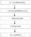
为解决上述问题,本发明提供一种超级结器件的晶圆背面工艺方法,是在晶圆上制作超级结器件的工艺,其包含如下的工艺步骤:In order to solve the above-mentioned problems, the present invention provides a process method for the backside of a wafer of a super junction device, which is a process for making a super junction device on a wafer, which includes the following process steps:
第1步,在半导体基材上刻蚀形成第一层沟槽并进行外延淀积填充;The first step is to etch the first layer of trenches on the semiconductor substrate and perform epitaxial deposition and filling;
第2步,进行N型外延层的牺牲氧化层淀积;The second step is to deposit the sacrificial oxide layer of the N-type epitaxial layer;
第3步,移除牺牲氧化层;Step 3, remove the sacrificial oxide layer;
第4步,进行晶圆背面的湿法刻蚀工艺;The fourth step is to carry out the wet etching process on the back of the wafer;
第5步,进行N型外延层的淀积;The fifth step is to deposit the N-type epitaxial layer;
第6步,再次刻蚀形成第二层沟槽。Step 6, etch again to form a second layer of trenches.
进一步的改进是,所述第1步中,半导体基材为硅衬底或者是硅外延层。A further improvement is that, in the first step, the semiconductor substrate is a silicon substrate or a silicon epitaxial layer.
进一步的改进是,所述的晶圆背面具有背面封膜层。A further improvement is that the backside of the wafer has a backside sealing film layer.
进一步的改进是,所述第5步的湿法刻蚀工艺能有效避免N型外延层淀积时对晶圆背面封膜层厚度的影响。A further improvement is that the wet etching process in the fifth step can effectively avoid the influence on the thickness of the sealing film layer on the backside of the wafer when the N-type epitaxial layer is deposited.
为解决上述问题,本发明提供一种超级结器件的晶圆背面工艺方法,包含如下的工艺步骤:In order to solve the above problems, the present invention provides a process method for the backside of a wafer of a super junction device, comprising the following process steps:
第1步,在半导体基材上刻蚀形成第一层沟槽并进行外延淀积填充;The first step is to etch the first layer of trenches on the semiconductor substrate and perform epitaxial deposition and filling;
第2步,进行N型外延层的牺牲氧化层淀积;The second step is to deposit the sacrificial oxide layer of the N-type epitaxial layer;
第3步,移除牺牲氧化层;Step 3, remove the sacrificial oxide layer;
第4步,进行N型外延层的淀积;The fourth step is to deposit the N-type epitaxial layer;
第5步,进行晶圆背面的湿法刻蚀工艺;The 5th step, carry out the wet etching process on the back of the wafer;
第6步,再次刻蚀形成第二层沟槽。Step 6, etch again to form a second layer of trenches.
进一步的改进是,所述第1步中,半导体基材为硅衬底或者是硅外延层。A further improvement is that, in the first step, the semiconductor substrate is a silicon substrate or a silicon epitaxial layer.
进一步的改进是,所述的晶圆背面具有背面封膜层。A further improvement is that the backside of the wafer has a backside sealing film layer.
进一步的改进是,所述第5步的湿法刻蚀工艺能提高背面封膜层的均匀性。A further improvement is that the wet etching process in the fifth step can improve the uniformity of the backside sealing film layer.
本发明所述的超级结器件的晶圆背面工艺方法,在N型外延层生长前或者N型外延层生长后加入背部多晶硅湿法刻蚀,可以有效的解决晶圆背面颗粒缺陷的问题。在N型外延层生长前可以有效的避免N型外延层作业时候对背面封膜层的厚度的影响,在N型外延层生长后再进行湿法刻蚀可以有效的避免背面封膜层厚度均匀性不好的问题。两种工艺都可以实现安全的解决背面缺陷的影响。The wafer backside processing method of the super junction device according to the present invention adds back polysilicon wet etching before the N-type epitaxial layer is grown or after the N-type epitaxial layer is grown, which can effectively solve the problem of particle defects on the wafer backside. Before the N-type epitaxial layer is grown, the influence of the N-type epitaxial layer on the thickness of the back sealing film can be effectively avoided. After the N-type epitaxial layer is grown, wet etching can effectively avoid the uniform thickness of the back sealing film. Sexual issues. Both processes can safely address the effects of backside defects.
附图说明Description of drawings
图1 是现有的超级结器件工艺中晶圆上沟槽刻蚀的工序示意图。FIG. 1 is a schematic diagram of a process of trench etching on a wafer in a conventional super junction device process.
图2 是本发明提供的超级结器件工艺中晶圆上沟槽刻蚀的工序示意图。FIG. 2 is a schematic diagram of a process of etching trenches on a wafer in the super junction device process provided by the present invention.
具体实施方式Detailed ways
本发明所述的超级结器件的晶圆背面工艺方法,是在晶圆上制作超级结器件的工艺,所述的晶圆背面已经贴附有背面封膜层。其包含如下的工艺步骤:The process method for the backside of the wafer of the super junction device according to the present invention is a process of making the superjunction device on the wafer, and the backside of the wafer has been attached with a backside sealing film. It includes the following process steps:
第1步,在半导体基材上,比如硅衬底或者硅外延层中刻蚀形成第一层沟槽,并进行外延淀积填充。In the first step, a first-layer trench is formed by etching on a semiconductor substrate, such as a silicon substrate or a silicon epitaxial layer, and is filled by epitaxial deposition.
第2步,进行N型外延层的牺牲氧化层淀积。由于材料表面可能存在一些缺陷,通过形成牺牲氧化层可以消除这些缺陷。In the second step, the sacrificial oxide layer is deposited on the N-type epitaxial layer. Since there may be some defects on the surface of the material, these defects can be eliminated by forming a sacrificial oxide layer.
第3步,移除牺牲氧化层。In step 3, the sacrificial oxide layer is removed.
第4步,进行晶圆背面的多晶硅的湿法刻蚀工艺。通过背部的湿法刻蚀,将多晶硅全部刻蚀掉。确保N型外延生长后背部没有多晶硅了,只有氧化膜层。In the fourth step, a wet etching process of polysilicon on the backside of the wafer is performed. All polysilicon is etched away by wet etching on the backside. Make sure that there is no polysilicon on the back after N-type epitaxial growth, only the oxide layer.
第5步,进行N型外延层的淀积。In step 5, the deposition of the N-type epitaxial layer is performed.
第6步,再次刻蚀形成第二层沟槽。Step 6, etch again to form a second layer of trenches.
本工艺在N型外延层淀积之前进行晶圆的背面多晶硅湿法刻蚀工艺,所述的湿法刻蚀工艺能有效避免N型外延层淀积时对晶圆背面封膜层厚度的影响。In this process, the polysilicon wet etching process on the back of the wafer is performed before the deposition of the N-type epitaxial layer, and the wet etching process can effectively avoid the influence on the thickness of the sealing film layer on the back of the wafer when the N-type epitaxial layer is deposited. .
本发明另提供一种超级结器件的晶圆背面工艺方法,包含如下的工艺步骤:The present invention further provides a wafer backside processing method for a super junction device, comprising the following process steps:
第1步,在硅衬底或者是硅外延层上刻蚀形成第一层沟槽,并进行外延淀积填充。The first step is to etch the first layer of trenches on the silicon substrate or the silicon epitaxial layer, and perform epitaxial deposition and filling.
第2步,进行N型外延层的牺牲氧化层淀积。In the second step, the sacrificial oxide layer is deposited on the N-type epitaxial layer.
第3步,移除牺牲氧化层。In step 3, the sacrificial oxide layer is removed.
第4步,进行N型外延层的淀积。In the fourth step, the deposition of the N-type epitaxial layer is performed.
第5步,进行晶圆背面的多晶硅的湿法刻蚀工艺。In step 5, a wet etching process of polysilicon on the backside of the wafer is performed.
第6步,再次刻蚀形成第二层沟槽。Step 6, etch again to form a second layer of trenches.
上述工艺方法与前一种相比,大部分工艺步骤相同,只是将背面的湿法刻蚀工艺步骤调整到N型外延层淀积之后,可以带来不同的技术效果。将背面湿法刻蚀工艺步骤后移,可以有效避免背面封膜层厚度均匀性不高的问题。Compared with the previous one, the above-mentioned process method has most of the same process steps, except that the wet etching process steps on the backside are adjusted to the deposition of the N-type epitaxial layer, which can bring about different technical effects. Moving the backside wet etching process step back can effectively avoid the problem of low uniformity of the thickness of the backside sealing film layer.
通过上述的工艺方法,在N型外延层生长前或者N型外延层生长后加入背部多晶硅湿法刻蚀,可以有效的解决晶圆背面颗粒缺陷的问题。在N型外延层生长前可以有效的避免N型外延层作业时候对背面封膜层的厚度的影响,在N型外延层生长后再进行湿法刻蚀可以有效的避免背面封膜层厚度均匀性不好的问题。两种工艺都可以实现安全的解决背面缺陷的影响。Through the above-mentioned process method, the backside polysilicon wet etching is added before the N-type epitaxial layer is grown or after the N-type epitaxial layer is grown, which can effectively solve the problem of particle defects on the backside of the wafer. Before the N-type epitaxial layer is grown, the influence of the N-type epitaxial layer on the thickness of the back sealing film can be effectively avoided. After the N-type epitaxial layer is grown, wet etching can effectively avoid the uniform thickness of the back sealing film. Sexual issues. Both processes can safely address the effects of backside defects.
以上仅为本发明的优选实施例,并不用于限定本发明。对于本领域的技术人员来说,本发明可以有各种更改和变化。凡在本发明的精神和原则之内,所作的任何修改、等同替换、改进等,均应包含在本发明的保护范围之内。The above are only preferred embodiments of the present invention, and are not intended to limit the present invention. Various modifications and variations of the present invention are possible for those skilled in the art. Any modification, equivalent replacement, improvement, etc. made within the spirit and principle of the present invention shall be included within the protection scope of the present invention.
Claims (8)
Priority Applications (1)
| Application Number | Priority Date | Filing Date | Title |
|---|---|---|---|
| CN201910089981.4ACN109698131B (en) | 2019-01-30 | 2019-01-30 | Wafer back process method of super junction device |
Applications Claiming Priority (1)
| Application Number | Priority Date | Filing Date | Title |
|---|---|---|---|
| CN201910089981.4ACN109698131B (en) | 2019-01-30 | 2019-01-30 | Wafer back process method of super junction device |
Publications (2)
| Publication Number | Publication Date |
|---|---|
| CN109698131A CN109698131A (en) | 2019-04-30 |
| CN109698131Btrue CN109698131B (en) | 2022-06-17 |
Family
ID=66234626
Family Applications (1)
| Application Number | Title | Priority Date | Filing Date |
|---|---|---|---|
| CN201910089981.4AActiveCN109698131B (en) | 2019-01-30 | 2019-01-30 | Wafer back process method of super junction device |
Country Status (1)
| Country | Link |
|---|---|
| CN (1) | CN109698131B (en) |
Families Citing this family (1)
| Publication number | Priority date | Publication date | Assignee | Title |
|---|---|---|---|---|
| CN112382556B (en)* | 2020-11-23 | 2022-10-28 | 华虹半导体(无锡)有限公司 | Manufacturing method of self-made wafer back sealing structure |
Citations (3)
| Publication number | Priority date | Publication date | Assignee | Title |
|---|---|---|---|---|
| US20090166722A1 (en)* | 2007-12-28 | 2009-07-02 | Alpha & Omega Semiconductor, Ltd: | High voltage structures and methods for vertical power devices with improved manufacturability |
| CN102403216A (en)* | 2010-09-09 | 2012-04-04 | 上海华虹Nec电子有限公司 | Method for fabricating superjunction devices using wet etching |
| CN109216155A (en)* | 2017-07-04 | 2019-01-15 | 上海新昇半导体科技有限公司 | A kind of method of back surface of the wafer sealing |
- 2019
- 2019-01-30CNCN201910089981.4Apatent/CN109698131B/enactiveActive
Patent Citations (3)
| Publication number | Priority date | Publication date | Assignee | Title |
|---|---|---|---|---|
| US20090166722A1 (en)* | 2007-12-28 | 2009-07-02 | Alpha & Omega Semiconductor, Ltd: | High voltage structures and methods for vertical power devices with improved manufacturability |
| CN102403216A (en)* | 2010-09-09 | 2012-04-04 | 上海华虹Nec电子有限公司 | Method for fabricating superjunction devices using wet etching |
| CN109216155A (en)* | 2017-07-04 | 2019-01-15 | 上海新昇半导体科技有限公司 | A kind of method of back surface of the wafer sealing |
Also Published As
| Publication number | Publication date |
|---|---|
| CN109698131A (en) | 2019-04-30 |
Similar Documents
| Publication | Publication Date | Title |
|---|---|---|
| CN108364870B (en) | Fabrication method of shielded gate trench MOSFET with improved gate oxide quality | |
| CN107359118B (en) | A kind of production method of super junction power device Withstand voltage layer | |
| JP2004273742A (en) | Method for manufacturing semiconductor wafer | |
| CN102820227B (en) | A kind of formation method of deep groove super PN junction | |
| US9570562B1 (en) | Method of planarizing polysilicon gate | |
| CN107818920B (en) | Gate oxide layer structure of shielded gate trench MOSFET and manufacturing method thereof | |
| CN107221561A (en) | A kind of lamination Electric Field Modulated high-voltage MOSFET structure and preparation method thereof | |
| CN109698131B (en) | Wafer back process method of super junction device | |
| CN107275389B (en) | Super junction trench filling method | |
| CN103928386B (en) | A kind of manufacture method of fleet plough groove isolation structure | |
| JP6458677B2 (en) | Manufacturing method and manufacturing apparatus for silicon carbide epitaxial wafer | |
| CN110429134A (en) | A kind of IGBT device and preparation method with asymmetric primitive unit cell | |
| CN109216156B (en) | Method for sealing wafer on back surface | |
| CN103137688A (en) | Semiconductor device with ditch groove metal oxide semiconductor (MOS) structure and manufacture method thereof | |
| JP6696247B2 (en) | Method of manufacturing semiconductor device | |
| CN105529355A (en) | Trench super junction epitaxial filling method | |
| CN104779162B (en) | A kind of method for improving trench VDMOS device gate oxide breakdown voltage | |
| CN102810501B (en) | Well region forming method and semiconductor substrate | |
| CN110767744A (en) | Super junction and manufacturing method thereof | |
| JP6558367B2 (en) | Semiconductor stack, semiconductor stack manufacturing method, and semiconductor device manufacturing method | |
| CN204289395U (en) | A kind of semiconductor device | |
| CN110224017A (en) | Super junction device structure and preparation method thereof | |
| CN103928325B (en) | Edge epitaxial planarization method of super junction devices | |
| CN109148266A (en) | epitaxial growth method | |
| CN110676220B (en) | Manufacturing method of groove type MOSFET, groove type MOSFET and electronic product |
Legal Events
| Date | Code | Title | Description |
|---|---|---|---|
| PB01 | Publication | ||
| PB01 | Publication | ||
| SE01 | Entry into force of request for substantive examination | ||
| SE01 | Entry into force of request for substantive examination | ||
| GR01 | Patent grant | ||
| GR01 | Patent grant |