CN109687138B - Antenna Based on Composite Left-Handed Unit Structure - Google Patents
Antenna Based on Composite Left-Handed Unit StructureDownload PDFInfo
- Publication number
- CN109687138B CN109687138BCN201910052309.8ACN201910052309ACN109687138BCN 109687138 BCN109687138 BCN 109687138BCN 201910052309 ACN201910052309 ACN 201910052309ACN 109687138 BCN109687138 BCN 109687138B
- Authority
- CN
- China
- Prior art keywords
- metal layer
- holes
- metallized
- bending
- rectangular
- Prior art date
- Legal status (The legal status is an assumption and is not a legal conclusion. Google has not performed a legal analysis and makes no representation as to the accuracy of the status listed.)
- Active
Links
- 239000002131composite materialSubstances0.000titleclaimsabstractdescription24
- 239000002184metalSubstances0.000claimsabstractdescription54
- 238000005452bendingMethods0.000claimsabstractdescription34
- 239000000758substrateSubstances0.000claimsabstractdescription34
- 238000001465metallisationMethods0.000claimsdescription26
- 238000012545processingMethods0.000abstractdescription4
- 230000005855radiationEffects0.000description6
- 230000005540biological transmissionEffects0.000description5
- 238000013461designMethods0.000description5
- 238000010586diagramMethods0.000description4
- 238000005259measurementMethods0.000description4
- 238000004891communicationMethods0.000description3
- 239000000463materialSubstances0.000description3
- 238000011161developmentMethods0.000description2
- 238000000034methodMethods0.000description2
- 238000004088simulationMethods0.000description2
- 230000002159abnormal effectEffects0.000description1
- 230000007547defectEffects0.000description1
- 230000009977dual effectEffects0.000description1
- 230000000694effectsEffects0.000description1
- 238000005516engineering processMethods0.000description1
- 230000010354integrationEffects0.000description1
- 238000011160researchMethods0.000description1
Images


Classifications
- H—ELECTRICITY
- H01—ELECTRIC ELEMENTS
- H01Q—ANTENNAS, i.e. RADIO AERIALS
- H01Q1/00—Details of, or arrangements associated with, antennas
- H01Q1/36—Structural form of radiating elements, e.g. cone, spiral, umbrella; Particular materials used therewith
- H01Q1/38—Structural form of radiating elements, e.g. cone, spiral, umbrella; Particular materials used therewith formed by a conductive layer on an insulating support
- H—ELECTRICITY
- H01—ELECTRIC ELEMENTS
- H01Q—ANTENNAS, i.e. RADIO AERIALS
- H01Q13/00—Waveguide horns or mouths; Slot antennas; Leaky-waveguide antennas; Equivalent structures causing radiation along the transmission path of a guided wave
- H01Q13/10—Resonant slot antennas
- H01Q13/18—Resonant slot antennas the slot being backed by, or formed in boundary wall of, a resonant cavity ; Open cavity antennas
Landscapes
- Waveguide Aerials (AREA)
Abstract
Translated fromChinese
Description
Translated fromChinese技术领域technical field
本发明涉及一种天线,尤其涉及一种复合左右手单元结构天线,属于微波技术领域。The invention relates to an antenna, in particular to a composite left and right hand unit structure antenna, which belongs to the technical field of microwaves.
背景技术Background technique
随着无线通信系统的发展,很多设备都要求能工作在2个或多个频段,因此双多频段天线成为近年来天线研究的热点。1999年,D.R. Smith等利用Pendry的理论制成了世界上第一块人工左手材料。2002年,Claoz和Itoh首次提出用传输线实现左手材料的新方法,复合左右手传输线作为左手材料的传输线实现形式,损耗低,易实现,具有多种异常特性和潜在应用价值,被广泛应用于微波工程设计中。With the development of wireless communication systems, many devices are required to work in two or more frequency bands, so dual multi-band antennas have become the focus of antenna research in recent years. In 1999, D.R. Smith et al. made the world's first artificial left-hand material using Pendry's theory. In 2002, Claoz and Itoh first proposed a new method of realizing left-handed materials with transmission lines. Composite left-handed transmission lines, as a form of transmission line realization of left-handed materials, have low loss, easy implementation, and have a variety of abnormal characteristics and potential application value, and are widely used in microwave engineering. designing.
然而,由于现代通信技术的迅速发展和应用,对通信系统的小型化、集成化提出了更高的要求,使得留给天线的空间越来越小。目前,虽然传统的天线在一定程度上减小了天线的尺寸,但是仍然存在带宽窄、增益小、辐射效率低、加工成本较高等问题,因此,本发明在传统的双频天线基础上,对天线结构进行改进,将双频天线改为单频天线,在保证天线辐射性能好、增益高的前提下,天线尺寸得到进一步地减小,且能达到满足多种天线场合的实际需求。However, due to the rapid development and application of modern communication technologies, higher requirements have been placed on the miniaturization and integration of communication systems, resulting in less and less space for antennas. At present, although the traditional antenna reduces the size of the antenna to a certain extent, there are still problems such as narrow bandwidth, low gain, low radiation efficiency, and high processing cost. Therefore, the present invention is based on the traditional dual-frequency antenna. The antenna structure is improved, and the dual-frequency antenna is changed to a single-frequency antenna. Under the premise of ensuring good antenna radiation performance and high gain, the size of the antenna is further reduced, and it can meet the actual needs of various antenna applications.
综上所述,如何提供一种天线尺寸更小的复合左右手单元结构天线,就成为本领域技术人员亟待解决的问题。To sum up, how to provide a composite left-handed unit structure antenna with a smaller antenna size has become an urgent problem to be solved by those skilled in the art.
发明内容SUMMARY OF THE INVENTION
本发明的目的是为了解决现有技术的上述缺陷,提出了一种复合左右手单元结构天线,在小型化、高增益电路中具有重要的应用价值。The purpose of the present invention is to solve the above-mentioned defects of the prior art, and propose a composite left-handed unit structure antenna, which has important application value in miniaturized and high-gain circuits.
本发明的技术解决方案是:The technical solution of the present invention is:
基于复合左右手单元结构的天线,包括介质基板、设置在介质基板顶层的顶层金属层、及设置在介质基板底层的底层金属层;所述顶层金属层的中心附近开设有折弯型槽,及顶层金属层的一侧设置有共面波导;所述介质基板上设置有一边开口的矩形区域,沿该矩形区域周向等距设置有多个第一金属化通孔,且在该矩形区域的内部设置有多排第二金属化通孔,所述顶层金属层与所述底层金属层通过金属化通孔相连通,介质基板、顶层金属层、底层金属层与金属化通孔形成矩形基片集成波导谐振腔;矩形基片集成波导谐振腔通过微带线与所述共面波导相连接;所述底层金属层上并列设置有两个矩形环槽,且每个矩形环槽的内部均设置有一贴片;An antenna based on a composite left and right-handed unit structure includes a dielectric substrate, a top metal layer disposed on the top layer of the dielectric substrate, and a bottom metal layer disposed on the bottom layer of the dielectric substrate; a bending groove is formed near the center of the top metal layer, and the top layer A coplanar waveguide is arranged on one side of the metal layer; a rectangular area with one side open is arranged on the dielectric substrate, and a plurality of first metallization through holes are arranged equidistantly along the circumferential direction of the rectangular area, and inside the rectangular area There are multiple rows of second metallized through holes, the top metal layer and the bottom metal layer are connected through the metallized through holes, and the dielectric substrate, the top metal layer, the bottom metal layer and the metallized through holes form a rectangular substrate integrated A waveguide resonator; a rectangular substrate integrated waveguide resonator is connected to the coplanar waveguide through a microstrip line; two rectangular ring grooves are arranged in parallel on the bottom metal layer, and each rectangular ring groove is internally provided with a patch;
所述折弯型槽包括多个折弯处,每个折弯处均对应一折弯开口,且折弯开口的开口方向向外,每个折弯处均为直角折弯;所述矩形区域的内部设置有两排第二金属化通孔,每排第二金属化通孔均包括三个第二金属化通孔,每个第二金属化通孔的直径与所述折弯开口宽度相同;The bending groove includes a plurality of bending positions, each bending position corresponds to a bending opening, and the opening direction of the bending opening is outward, and each bending position is a right-angle bending; the rectangular area There are two rows of second metallization through holes inside, each row of second metallization through holes includes three second metallization through holes, and the diameter of each second metallization through hole is the same as the width of the bending opening ;
每个所述第二金属化通孔均位于所述折弯处在介质基板上的投影位置。Each of the second metallization through holes is located at a projected position of the bending portion on the dielectric substrate.
优选地,所述顶层金属层的一侧开设有凹口,凹口的一侧与所述共面波导的中心导带相连接,且所述凹口的尺寸与所述矩形区域一边的开口尺寸相匹配。Preferably, a notch is formed on one side of the top metal layer, one side of the notch is connected with the central conducting strip of the coplanar waveguide, and the size of the notch is the same as the size of the opening on one side of the rectangular area match.
优选地,所述共面波导的中心导带与所述顶层金属层共面,并与凹口两侧的顶层金属层形成共面波导,所述微带线与共面波导的中心导带相连接,且矩形基片集成波导谐振腔通过微带线与所述共面波导相连接。Preferably, the central conducting strip of the coplanar waveguide is coplanar with the top metal layer, and forms a coplanar waveguide with the top metal layers on both sides of the notch, and the microstrip line is connected to the central conducting strip of the coplanar waveguide , and the rectangular substrate integrated waveguide resonator is connected with the coplanar waveguide through a microstrip line.
优选地,所述凹口的开口方向与所述矩形区域一边开口的开口方向相同。Preferably, the opening direction of the notch is the same as the opening direction of one side of the rectangular area.
优选地,所述贴片的长度小于所述矩形环槽的长度,所述贴片的宽度小于所述矩形环槽的宽度。Preferably, the length of the patch is smaller than the length of the rectangular ring groove, and the width of the patch is smaller than the width of the rectangular ring groove.
优选地,所述贴片的宽度与所述第二金属化通孔的直径相同。Preferably, the width of the patch is the same as the diameter of the second metallized through hole.
优选地,所述第一金属化通孔的直径大于等于相邻两个所述第一金属化通孔之间的间距的二分之一。Preferably, the diameter of the first metallization through hole is greater than or equal to half of the distance between two adjacent first metallization through holes.
本发明与现有技术相比,具有以下技术效果:本发明公开的一种基于新型复合左右手单元结构的天线,在保留了传统背腔缝隙天线高辐射性能优点的基础上,进一步缩小了天线尺寸,降低了天线的加工成本,更易于和平面电路集成。且本发明的新型复合左右手单元结构比传统复合左右手天线更紧凑,尺寸不变的情况下,有更低的工作频点。另外,本发明复合左右手传输线的零阶或负数阶谐振特性可以有效的突破传统天线在设计上受谐振波长的限制,在天线小型化设计中有极大的应用价值。Compared with the prior art, the present invention has the following technical effects: an antenna based on a novel composite left and right hand unit structure disclosed in the present invention further reduces the size of the antenna on the basis of retaining the advantages of the high radiation performance of the traditional cavity-backed slot antenna , reduces the processing cost of the antenna, and is easier to integrate with the plane circuit. In addition, the structure of the novel composite left and right-handed unit of the present invention is more compact than the traditional composite left and right-handed antenna, and under the condition of the same size, it has a lower working frequency. In addition, the zero-order or negative-order resonance characteristics of the composite left and right-handed transmission line of the present invention can effectively break through the limitation of the resonance wavelength in the design of traditional antennas, and have great application value in the design of antenna miniaturization.
以下便结合实施例附图,对本发明的具体实施方式作进一步的详述,以使本发明技术方案更易于理解、掌握。The specific embodiments of the present invention will be further described in detail below in conjunction with the accompanying drawings of the embodiments, so as to make the technical solutions of the present invention easier to understand and grasp.
附图说明Description of drawings
图1是本发明的结构示意图;Fig. 1 is the structural representation of the present invention;
图2是本发明的俯视结构示意图;Fig. 2 is the top view structure schematic diagram of the present invention;
图3是本发明的仰视结构示意图;Fig. 3 is the bottom view structure schematic diagram of the present invention;
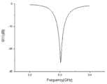
图4是本实施例的仿真和测量的S参数图;Fig. 4 is the S-parameter diagram of the simulation and measurement of the present embodiment;
图5是本实施例在3.31GHz频段下的仿真E面和H面增益方向图。FIG. 5 is the simulated E-plane and H-plane gain patterns in the 3.31 GHz frequency band of this embodiment.
其中,1-顶层金属层,11-折弯型槽,111-折弯处,12-凹口 13-中心导带,2-介质基板,21-矩形区域, 22-第一金属化通孔,23-第二金属化通孔,24-开口,3-底层金属层,31-矩形环槽,311-贴片。Among them, 1-top metal layer, 11-bending groove, 111-bending place, 12-notch 13-center conduction band, 2-dielectric substrate, 21-rectangular area, 22-first metallized through hole, 23-second metallized through hole, 24-opening, 3-bottom metal layer, 31-rectangular ring groove, 311-patch.
具体实施方式Detailed ways
基于复合左右手单元结构的天线,如图1-图3所示,包括介质基板2、设置在介质基板2顶层的顶层金属层1、及设置在介质基板2底层的底层金属层3;顶层金属层1的中心附近开设有折弯型槽11,折弯型槽11包括多个折弯处111,每个折弯处111均对应一折弯开口,且折弯开口的开口方向向外,每个折弯处111均为直角折弯。在本实施例中,该折弯型槽11包括六个折弯处111。The antenna based on the composite left-handed unit structure, as shown in Figures 1-3, includes a
顶层金属层1的一侧设置有共面波导,顶层金属层1的一侧开设有凹口12,凹口12的一侧与共面波导的中心导带13相连接,如图1-图2所示,中心导带13通过凹口12的一侧与顶层金属层1相连接且中心导带13与顶层金属层1一体成型,中心导带13与顶层金属层1共面,并与凹口12两侧的顶层金属层1形成共面波导,在本发明的技术方案中,为了方便测量,在中心导带13处设置有微带线(图中未示出),微带线与共面波导的中心导带13相连接,中心导带13为中心金属条带,且微带线为50欧姆微带线,中心金属条与50欧姆微带线相重合。为了满足阻抗匹配要求,可以改变共面波导深入谐振腔的长度,以达到降低反射系数的目的,而微带线和共面波导相连,是为了测量的方便。One side of the
介质基板2上设置有一边开口24的矩形区域21,沿该矩形区域21周向等距设置有多个第一金属化通孔22,且在该矩形区域21的内部设置有多排第二金属化通孔23,顶层金属层1与底层金属层3通过金属化通孔相连通,介质基板2、顶层金属层1、底层金属层3与金属化通孔形成矩形基片集成波导谐振腔;矩形基片集成波导谐振腔通过微带线与共面波导相连接;在本实施例中,介质基板2为Rogers5880,介质基板2上设置为一边开口24的正方形区域,正方形区域的四个顶点处,即第一顶点、第二顶点、第三顶点及第四顶点处均设置有一个第一金属化通孔22,该凹口12开设在第一顶点与第二顶点之间,第一顶点与凹口12的一侧设置有两个第一金属化通孔22,第一顶点与第四顶点、第四顶点与第三顶点、第三顶点与第二顶点之间均设置有九个第一金属化通孔22。为了使能量泄露被抑制到几乎可以忽略的程度,第一金属化通孔22的直径大于等于相邻两个所述第一金属化通孔22之间的间距的二分之一,且介质基板2的厚度要远远小于介质波长,本发明优选为第一金属化通孔22的直径等于相邻两个第一金属化通孔22之间的间距的二分之一。The
凹口12的开口方向与矩形区域21一边开口24的开口方向相同,且凹口12的尺寸与矩形区域21一边的开口24尺寸相匹配,即开口24的宽度大于或等于凹口12的宽度。The opening direction of the
在本发明的技术方案中,矩形区域21的内部设置有两排第二金属化通孔23,每排第二金属化通孔23均包括三个等距设置的第二金属化通孔23,每个第二金属化通孔23的直径与折弯开口宽度相同,每个第二金属化通孔23均位于折弯处111在介质基板2上的投影位置。In the technical solution of the present invention, two rows of second metallization through
进一步地,底层金属层3上并列设置有两个矩形环槽31,且每个矩形环槽31的内部均设置有一贴片311;贴片311的长度小于矩形环槽31的长度,贴片311的宽度小于矩形环槽31的宽度,且贴片311的宽度与第二金属化通孔23的直径相同。当顶层金属层1、底层金属层3与介质基板2叠合在一起时,从图2中可看出,第二金属化通孔23设置在折弯型槽11的折弯处111,从图3中可看出,第二金属化通孔23设置在贴片311内。Further, two
本实施例中还利用三维电磁仿真软件对所提出的天线结构进行仿真,如图4至图5所示,图4是本发明实施例的仿真和测量的S参数图,从图4可以看出,在工作带宽内,天线回波损耗最低达到-27dB,所以满足阻抗匹配要求。图5是本实施例仿真的E面增益方向图和H面增益方向图,从图5中可以看出,天线的辐射性能较好,辐射效率高。在基片集成波导结合型复合左右手单元结构的天线设计和应用中具有巨大的参考价值。In this embodiment, three-dimensional electromagnetic simulation software is also used to simulate the proposed antenna structure, as shown in FIG. 4 to FIG. 5 , FIG. 4 is the S-parameter diagram of the simulation and measurement according to the embodiment of the present invention, and it can be seen from FIG. 4 , within the working bandwidth, the antenna return loss is at least -27dB, so it meets the impedance matching requirements. FIG. 5 is the E-plane gain pattern and the H-plane gain pattern simulated in this embodiment. It can be seen from FIG. 5 that the antenna has good radiation performance and high radiation efficiency. It has great reference value in the antenna design and application of the substrate-integrated-waveguide-combined composite left-handed unit structure.
本发明公开的一种基于新型复合左右手单元结构的天线,在保留了传统背腔缝隙天线高辐射性能优点的基础上,进一步缩小了天线尺寸,降低了天线的加工成本,更易于和平面电路集成。且本发明的新型复合左右手单元结构比传统复合左右手天线更紧凑,尺寸不变的情况下,有更低的工作频点。另外,本发明复合左右手传输线的零阶或负数阶谐振特性可以有效的突破传统天线在设计上受谐振波长的限制,在天线小型化设计中有极大的应用价值。The invention discloses an antenna based on a novel composite left and right-handed unit structure, which further reduces the size of the antenna, reduces the processing cost of the antenna, and is easier to integrate with the plane circuit on the basis of retaining the advantages of the high radiation performance of the traditional cavity-backed slot antenna. . In addition, the structure of the novel composite left and right-handed unit of the present invention is more compact than the traditional composite left and right-handed antenna, and under the condition of the same size, it has a lower working frequency. In addition, the zero-order or negative-order resonance characteristics of the composite left and right-handed transmission line of the present invention can effectively break through the limitation of the resonance wavelength in the design of traditional antennas, and have great application value in the design of antenna miniaturization.
应该注意的是,上述实施例对本发明进行说明而不是对本发明进行限制,并且本领域技术人员在不脱离所附权利要求的范围的情况下可设计出替换实施例。It should be noted that the above-described embodiments illustrate rather than limit the invention, and that alternative embodiments may be devised by those skilled in the art without departing from the scope of the appended claims.
Claims (7)
Translated fromChinesePriority Applications (1)
| Application Number | Priority Date | Filing Date | Title |
|---|---|---|---|
| CN201910052309.8ACN109687138B (en) | 2019-01-21 | 2019-01-21 | Antenna Based on Composite Left-Handed Unit Structure |
Applications Claiming Priority (1)
| Application Number | Priority Date | Filing Date | Title |
|---|---|---|---|
| CN201910052309.8ACN109687138B (en) | 2019-01-21 | 2019-01-21 | Antenna Based on Composite Left-Handed Unit Structure |
Publications (2)
| Publication Number | Publication Date |
|---|---|
| CN109687138A CN109687138A (en) | 2019-04-26 |
| CN109687138Btrue CN109687138B (en) | 2020-10-02 |
Family
ID=66193787
Family Applications (1)
| Application Number | Title | Priority Date | Filing Date |
|---|---|---|---|
| CN201910052309.8AActiveCN109687138B (en) | 2019-01-21 | 2019-01-21 | Antenna Based on Composite Left-Handed Unit Structure |
Country Status (1)
| Country | Link |
|---|---|
| CN (1) | CN109687138B (en) |
Families Citing this family (1)
| Publication number | Priority date | Publication date | Assignee | Title |
|---|---|---|---|---|
| CN111048879B (en)* | 2019-12-31 | 2025-06-06 | 广东盛路通信有限公司 | A broadband constant amplitude conversion structure from rectangular waveguide to double-terminal stripline |
Citations (2)
| Publication number | Priority date | Publication date | Assignee | Title |
|---|---|---|---|---|
| CN102074795A (en)* | 2011-01-21 | 2011-05-25 | 杭州电子科技大学 | Dual circular polarization reconfigurable antenna |
| CN108923126A (en)* | 2018-06-26 | 2018-11-30 | 西安电子科技大学 | A kind of four molds based on substrate integration wave-guide have the filter antenna of double zero points |
Family Cites Families (1)
| Publication number | Priority date | Publication date | Assignee | Title |
|---|---|---|---|---|
| US9711860B2 (en)* | 2015-08-13 | 2017-07-18 | Sony Corporation | Wideband antennas including a substrate integrated waveguide |
- 2019
- 2019-01-21CNCN201910052309.8Apatent/CN109687138B/enactiveActive
Patent Citations (2)
| Publication number | Priority date | Publication date | Assignee | Title |
|---|---|---|---|---|
| CN102074795A (en)* | 2011-01-21 | 2011-05-25 | 杭州电子科技大学 | Dual circular polarization reconfigurable antenna |
| CN108923126A (en)* | 2018-06-26 | 2018-11-30 | 西安电子科技大学 | A kind of four molds based on substrate integration wave-guide have the filter antenna of double zero points |
Non-Patent Citations (1)
| Title |
|---|
| 《A miniaturized dual mode CRLH unit cell loaded SIW antenna》;Sourav Nandi,Akhilesh Mohan;《2015 IEEE Applied Electromagnetics Conference (AEMC)》;20151221;1-2* |
Also Published As
| Publication number | Publication date |
|---|---|
| CN109687138A (en) | 2019-04-26 |
Similar Documents
| Publication | Publication Date | Title |
|---|---|---|
| CN107134653B (en) | A Planar Compact Slot Antenna Array Based on Substrate Integrated Waveguide Resonator | |
| CN103840271B (en) | Multi-frequency-band cavity-backed half-mode substrate integrated waveguide bent slot antenna | |
| US8665158B2 (en) | Printed filtering antenna | |
| CN110544822A (en) | Ka-band Miniaturized Filter Antenna Based on SIW Structure | |
| CN112436295A (en) | Millimeter wave high-gain high-radiation-efficiency slot antenna array based on ridge gap waveguide | |
| CN110957575B (en) | A Surface Plasmon Structure Sharing Large Frequency Ratio Dual-Band Antenna | |
| CN105226355B (en) | High parasitic band suppression a quarter mould substrate integration wave-guide frequency-selective surfaces | |
| CN110021805A (en) | Based on the three-dimensional transition structure of the air gap waveguide in complicated feed network | |
| CN103178341B (en) | Indoor high-speed communication antenna of wide-beam Q-band millimeter waves | |
| CN109546348A (en) | A kind of novel miniaturization broadband SW-SIW electromagnetic horn and its design method | |
| CN201975513U (en) | Ultra wide band antenna of integrated filter | |
| CN108879090A (en) | Half cylindrical cavity miniature antenna of half module substrate integrated wave guide | |
| CN117855859A (en) | Broadband Huygens super-surface unit, transmission array antenna and design method | |
| CN116093629A (en) | A wind-shaped metasurface antenna with broadband stable radiation characteristics | |
| CN109687138B (en) | Antenna Based on Composite Left-Handed Unit Structure | |
| CN110429380A (en) | It is applied towards 5G and two unit micro-strip mimo antennas is shared based on irradiation structure | |
| CN209843960U (en) | Back-cavity gap circularly polarized millimeter wave antenna of Substrate Integrated Waveguide (SIW) | |
| CN101640315A (en) | Dual stop band ultra wide band antenna based on dual U-shaped defected ground structure | |
| WO2025043932A1 (en) | Miniaturized open-cavity broadband antenna based on substrate-integrated waveguide | |
| CN106571517B (en) | A kind of microminiature flat plane antenna based on metamaterial structure | |
| CN101707284B (en) | LTCC electrically small integrated antenna for radio-frequency front-end system | |
| CN107634321A (en) | Composite left and right flashlight small antenna based on triangular resonator | |
| Esfandiarpour et al. | Wideband planar horn antenna using substrate integrated waveguide technique | |
| CN116207468B (en) | A broadband balun based on rectangular waveguide to microstrip gap waveguide | |
| Roopa | Cavity Backed Multiband SIW Antenna for X Band Applications |
Legal Events
| Date | Code | Title | Description |
|---|---|---|---|
| PB01 | Publication | ||
| PB01 | Publication | ||
| SE01 | Entry into force of request for substantive examination | ||
| SE01 | Entry into force of request for substantive examination | ||
| CB02 | Change of applicant information | ||
| CB02 | Change of applicant information | Address after:210003 Gulou District, Jiangsu, Nanjing new model road, No. 66 Applicant after:NANJING University OF POSTS AND TELECOMMUNICATIONS Address before:210023 Jiangsu city of Nanjing province Ya Dong new Yuen Road No. 9 Applicant before:NANJING University OF POSTS AND TELECOMMUNICATIONS | |
| GR01 | Patent grant | ||
| GR01 | Patent grant |