CN109669323B - A method for realizing large-area super-resolution lithography based on resonant cavity structure - Google Patents
A method for realizing large-area super-resolution lithography based on resonant cavity structureDownload PDFInfo
- Publication number
- CN109669323B CN109669323BCN201811510455.2ACN201811510455ACN109669323BCN 109669323 BCN109669323 BCN 109669323BCN 201811510455 ACN201811510455 ACN 201811510455ACN 109669323 BCN109669323 BCN 109669323B
- Authority
- CN
- China
- Prior art keywords
- resonant cavity
- cavity structure
- layer
- interference
- lithography
- Prior art date
- Legal status (The legal status is an assumption and is not a legal conclusion. Google has not performed a legal analysis and makes no representation as to the accuracy of the status listed.)
- Active
Links
- 238000001459lithographyMethods0.000titleclaimsabstractdescription26
- 238000000034methodMethods0.000titleclaimsabstractdescription26
- 239000000463materialSubstances0.000claimsabstractdescription50
- 229910052751metalInorganic materials0.000claimsabstractdescription32
- 239000002184metalSubstances0.000claimsabstractdescription32
- 238000005286illuminationMethods0.000claimsabstractdescription27
- 238000002834transmittanceMethods0.000claimsabstractdescription10
- 239000000758substrateSubstances0.000claimsabstractdescription8
- 229910052782aluminiumInorganic materials0.000claimsdescription11
- XAGFODPZIPBFFR-UHFFFAOYSA-NaluminiumChemical compound[Al]XAGFODPZIPBFFR-UHFFFAOYSA-N0.000claimsdescription11
- 239000002210silicon-based materialSubstances0.000claimsdescription11
- 238000009826distributionMethods0.000claimsdescription6
- 230000005284excitationEffects0.000claimsdescription5
- BQCADISMDOOEFD-UHFFFAOYSA-NSilverChemical compound[Ag]BQCADISMDOOEFD-UHFFFAOYSA-N0.000claimsdescription4
- PCHJSUWPFVWCPO-UHFFFAOYSA-NgoldChemical compound[Au]PCHJSUWPFVWCPO-UHFFFAOYSA-N0.000claimsdescription4
- 229910052737goldInorganic materials0.000claimsdescription4
- 239000010931goldSubstances0.000claimsdescription4
- 229910052709silverInorganic materials0.000claimsdescription4
- 239000004332silverSubstances0.000claimsdescription4
- 238000000206photolithographyMethods0.000claimsdescription3
- 230000010287polarizationEffects0.000claimsdescription3
- 229910052710siliconInorganic materials0.000abstractdescription36
- 239000010703siliconSubstances0.000abstractdescription36
- XUIMIQQOPSSXEZ-UHFFFAOYSA-NSiliconChemical compound[Si]XUIMIQQOPSSXEZ-UHFFFAOYSA-N0.000abstractdescription34
- 238000000025interference lithographyMethods0.000abstractdescription18
- 230000000694effectsEffects0.000abstractdescription5
- 238000002360preparation methodMethods0.000abstractdescription3
- 229920002120photoresistant polymerPolymers0.000description32
- 239000010408filmSubstances0.000description25
- 238000005530etchingMethods0.000description21
- 238000010586diagramMethods0.000description19
- 238000012545processingMethods0.000description12
- 238000012546transferMethods0.000description10
- 238000005516engineering processMethods0.000description8
- 239000008204material by functionSubstances0.000description7
- 239000012954diazoniumSubstances0.000description6
- 150000001989diazonium saltsChemical class0.000description6
- 230000000873masking effectEffects0.000description5
- 230000000737periodic effectEffects0.000description5
- 238000001020plasma etchingMethods0.000description5
- CSCPPACGZOOCGX-UHFFFAOYSA-NAcetoneChemical compoundCC(C)=OCSCPPACGZOOCGX-UHFFFAOYSA-N0.000description4
- 238000004088simulationMethods0.000description4
- VEXZGXHMUGYJMC-UHFFFAOYSA-MChloride anionChemical compound[Cl-]VEXZGXHMUGYJMC-UHFFFAOYSA-M0.000description3
- 239000011248coating agentSubstances0.000description3
- 238000000576coating methodMethods0.000description3
- 239000002609mediumSubstances0.000description3
- 238000004528spin coatingMethods0.000description3
- 239000010409thin filmSubstances0.000description3
- 230000007547defectEffects0.000description2
- 238000010894electron beam technologyMethods0.000description2
- 239000007769metal materialSubstances0.000description2
- 150000002739metalsChemical class0.000description2
- 230000000704physical effectEffects0.000description2
- 239000010453quartzSubstances0.000description2
- 238000011160researchMethods0.000description2
- VYPSYNLAJGMNEJ-UHFFFAOYSA-Nsilicon dioxideInorganic materialsO=[Si]=OVYPSYNLAJGMNEJ-UHFFFAOYSA-N0.000description2
- 239000000126substanceSubstances0.000description2
- 230000003321amplificationEffects0.000description1
- 230000033228biological regulationEffects0.000description1
- 230000005540biological transmissionEffects0.000description1
- 238000006243chemical reactionMethods0.000description1
- 238000002508contact lithographyMethods0.000description1
- 238000011109contaminationMethods0.000description1
- 239000013078crystalSubstances0.000description1
- 238000000151depositionMethods0.000description1
- 238000013461designMethods0.000description1
- 238000000609electron-beam lithographyMethods0.000description1
- 238000001704evaporationMethods0.000description1
- 239000003574free electronSubstances0.000description1
- 238000003384imaging methodMethods0.000description1
- 238000010884ion-beam techniqueMethods0.000description1
- 238000001755magnetron sputter depositionMethods0.000description1
- 238000004519manufacturing processMethods0.000description1
- 238000005329nanolithographyMethods0.000description1
- 238000003199nucleic acid amplification methodMethods0.000description1
- 230000010355oscillationEffects0.000description1
- 238000000059patterningMethods0.000description1
- 238000003672processing methodMethods0.000description1
- 230000003362replicative effectEffects0.000description1
Images


Classifications
- G—PHYSICS
- G03—PHOTOGRAPHY; CINEMATOGRAPHY; ANALOGOUS TECHNIQUES USING WAVES OTHER THAN OPTICAL WAVES; ELECTROGRAPHY; HOLOGRAPHY
- G03F—PHOTOMECHANICAL PRODUCTION OF TEXTURED OR PATTERNED SURFACES, e.g. FOR PRINTING, FOR PROCESSING OF SEMICONDUCTOR DEVICES; MATERIALS THEREFOR; ORIGINALS THEREFOR; APPARATUS SPECIALLY ADAPTED THEREFOR
- G03F7/00—Photomechanical, e.g. photolithographic, production of textured or patterned surfaces, e.g. printing surfaces; Materials therefor, e.g. comprising photoresists; Apparatus specially adapted therefor
- G03F7/20—Exposure; Apparatus therefor
- G03F7/2022—Multi-step exposure, e.g. hybrid; backside exposure; blanket exposure, e.g. for image reversal; edge exposure, e.g. for edge bead removal; corrective exposure
- G—PHYSICS
- G03—PHOTOGRAPHY; CINEMATOGRAPHY; ANALOGOUS TECHNIQUES USING WAVES OTHER THAN OPTICAL WAVES; ELECTROGRAPHY; HOLOGRAPHY
- G03F—PHOTOMECHANICAL PRODUCTION OF TEXTURED OR PATTERNED SURFACES, e.g. FOR PRINTING, FOR PROCESSING OF SEMICONDUCTOR DEVICES; MATERIALS THEREFOR; ORIGINALS THEREFOR; APPARATUS SPECIALLY ADAPTED THEREFOR
- G03F7/00—Photomechanical, e.g. photolithographic, production of textured or patterned surfaces, e.g. printing surfaces; Materials therefor, e.g. comprising photoresists; Apparatus specially adapted therefor
- G03F7/70—Microphotolithographic exposure; Apparatus therefor
- G03F7/70425—Imaging strategies, e.g. for increasing throughput or resolution, printing product fields larger than the image field or compensating lithography- or non-lithography errors, e.g. proximity correction, mix-and-match, stitching or double patterning
- G03F7/70466—Multiple exposures, e.g. combination of fine and coarse exposures, double patterning or multiple exposures for printing a single feature
- G—PHYSICS
- G03—PHOTOGRAPHY; CINEMATOGRAPHY; ANALOGOUS TECHNIQUES USING WAVES OTHER THAN OPTICAL WAVES; ELECTROGRAPHY; HOLOGRAPHY
- G03F—PHOTOMECHANICAL PRODUCTION OF TEXTURED OR PATTERNED SURFACES, e.g. FOR PRINTING, FOR PROCESSING OF SEMICONDUCTOR DEVICES; MATERIALS THEREFOR; ORIGINALS THEREFOR; APPARATUS SPECIALLY ADAPTED THEREFOR
- G03F7/00—Photomechanical, e.g. photolithographic, production of textured or patterned surfaces, e.g. printing surfaces; Materials therefor, e.g. comprising photoresists; Apparatus specially adapted therefor
- G03F7/70—Microphotolithographic exposure; Apparatus therefor
Landscapes
- Physics & Mathematics (AREA)
- General Physics & Mathematics (AREA)
- Diffracting Gratings Or Hologram Optical Elements (AREA)
Abstract
Translated fromChinese
Description
Translated fromChinese技术领域technical field
本发明属于微纳光刻加工技术及微纳器件加工领域,具体涉及一种基于共振腔结构实现大面积超分辨光刻方法。The invention belongs to the field of micro-nano lithography processing technology and micro-nano device processing, and particularly relates to a large-area super-resolution lithography method based on a resonance cavity structure.
背景技术Background technique
光的干涉是光波动性的基本特征。当两束光波的频率相同,振动方向相同,并且拥有固定不变的相位差时,就能形成稳定的明暗交替的干涉条纹。这种强度周期性变化的条纹如果记录在感光层上会呈现出厚度周期性变化的图样,从而实现“光刻”,激光干涉技术就是基于此种原理。该技术具有无需掩模,大视场,长焦深等特点,现广泛应用于很多纳米图形及纳米器件加工等领域。激光干涉技术的分辨力d=λ/(2sinθ),对比密集(L/S=1:1)结构,干涉光刻的极限CD为λ/4。显然,想要获得更高的分辨力,只有采用更短的激发波长。The interference of light is the basic feature of the wave nature of light. When the two light waves have the same frequency, the same vibration direction, and have a constant phase difference, stable interference fringes with alternating light and dark can be formed. If such stripes with periodic intensity changes are recorded on the photosensitive layer, they will show a pattern of periodic thickness changes, thus realizing "photolithography". Laser interference technology is based on this principle. This technology has the characteristics of no mask, large field of view, long focal depth, etc., and is now widely used in many fields such as nano-patterning and nano-device processing. The resolution of laser interference technology is d=λ/(2sinθ), the contrast is dense (L/S=1:1) structure, and the limit CD of interference lithography is λ/4. Obviously, to obtain higher resolution, only a shorter excitation wavelength can be used.
表面等离子体(surface plasmon,SP)是金属中的自由电子受到外界的电磁扰动,在金属和介质的表面产生集体振荡的行为。和自由空间中的光波相比,SP具有短波长特性。利用该特性,罗先刚课题组使用周期300nm,缝宽50nm的Ag光栅,在436nm工作波长下获得了周期100nm的干涉条纹。之后,有研究小组利用金属-介质-金属的共振腔模式增强了干涉条纹的对比度,将激发光源进一步缩小到193nm的时候,模拟仿真上可获得22nm的分辨力。金属-介质-金属的共振腔模式利用底层金属对倏逝波的进一步共振放大可实现高分辨力、高对比度的干涉图形,但是考虑到共振腔的共振作用,中间介质层的厚度一般在50nm及以下,这就为金属图形的传递带来了困难。因为就一般金属材料而言,其和光刻胶的刻蚀比都很低。因此本发明提出了利用硅基材料代替原有共振腔结构中的底层金属,本方法可以利用深硅刻蚀工艺直接制备硅基器件,同时也可以用硅作为中间传递刻蚀的掩蔽层实现其他材料的刻蚀制备。Surface plasmon (SP) is a behavior in which free electrons in metals are subjected to external electromagnetic disturbances to generate collective oscillations on the surfaces of metals and media. Compared with light waves in free space, SPs have short wavelength characteristics. Taking advantage of this characteristic, Luo Xiangang's research group used an Ag grating with a period of 300 nm and a slit width of 50 nm, and obtained interference fringes with a period of 100 nm at a working wavelength of 436 nm. After that, a research group used the metal-dielectric-metal resonant cavity mode to enhance the contrast of the interference fringes, and when the excitation light source was further reduced to 193 nm, the resolution of 22 nm was obtained in the simulation. The metal-dielectric-metal resonant cavity mode utilizes the further resonance amplification of the evanescent wave by the underlying metal to achieve high-resolution and high-contrast interference patterns. However, considering the resonance effect of the resonant cavity, the thickness of the intermediate dielectric layer is generally 50 nm and Hereinafter, this brings difficulties to the transfer of the metal pattern. Because for general metal materials, its etching ratio to photoresist is very low. Therefore, the present invention proposes to use silicon-based material to replace the underlying metal in the original resonant cavity structure. This method can directly prepare silicon-based devices by using a deep silicon etching process, and can also use silicon as a masking layer for intermediate transfer etching to achieve other Etching preparation of materials.
另一方面,传统用于激发共振腔体中表面等离子体干涉的光栅是用电子束光刻或者聚焦离子束加工的,在大面积加工方面成本昂贵。在本发明中,利用廉价的激光干涉技术获得周期性的光场使特殊感光材料的透过率或/和折射率发生改变,进而用作第二次表面等离子体干涉光刻的激发光栅。最终利用表面等离子体的短波长特性获得分辨力为百纳米及以下的大面积干涉图形,因此本发明也提供了一种百纳米量级以下大面积硅掩模的廉价制备方法。On the other hand, gratings traditionally used to excite surface plasmon interference in resonant cavities are fabricated with electron beam lithography or focused ion beams, which are expensive in large-area fabrication. In the present invention, a periodic light field is obtained by using an inexpensive laser interference technology to change the transmittance or/and the refractive index of the special photosensitive material, which is then used as an excitation grating for the second surface plasmon interference lithography. Finally, a large-area interference pattern with a resolution of 100 nanometers or less is obtained by utilizing the short wavelength characteristics of surface plasmons. Therefore, the present invention also provides an inexpensive preparation method for a large-area silicon mask of the order of 100 nanometers or less.
发明内容SUMMARY OF THE INVENTION
本发明的要解决的技术问题为:The technical problem to be solved by the present invention is:
(1)、目前大面积纳米图形掩模加工大都采用电子束加工的方式,本发明提供了一种120nm及以下周期大面积密集掩模加工的替代技术,能解决大面积纳米图形加工昂贵的问题;(1) At present, most of the large-area nano-pattern mask processing adopts the method of electron beam processing. The present invention provides an alternative technology for large-area intensive mask processing with a period of 120 nm and below, which can solve the problem that large-area nano-pattern processing is expensive. ;
(2)、表面等离子体光刻虽能实现较高的分辨力,但大都采用接触的光刻模式,这样会带来掩模的污染和损伤问题,减小掩模的使用寿命;(2) Although surface plasma lithography can achieve higher resolution, most of them use the contact lithography mode, which will bring pollution and damage to the mask and reduce the service life of the mask;
(3)、表面等离子体光刻中,掩模与光刻基片均为硬质材料,即便在压力作用下接触,二者因面形的差异必然存在厚度不均的间隙分布,从而影响表面等离子体光刻的成像对比度,从而导致大面积图形光刻效果分布差异,甚至严重缺陷。(3) In surface plasma lithography, the mask and the lithography substrate are both hard materials. Even if they are in contact under pressure, there must be a gap distribution with uneven thickness due to the difference in surface shape, which affects the surface. The imaging contrast of plasma lithography leads to differences in the distribution of large-area pattern lithography effects, and even serious defects.
(4)、表面等离子体光刻中传统的共振腔一般由金属-介质-金属组成的腔体结构构成,在实际应用中需要刻蚀底层金属后才能实现功能材料的传递,这样会带来光刻线条线边缘粗糙度增大,也会带来一定的金属污染问题。(4) The traditional resonant cavity in surface plasmon lithography is generally composed of a cavity structure composed of metal-dielectric-metal. In practical applications, it is necessary to etch the underlying metal to realize the transfer of functional materials, which will bring light The increased roughness of the edge of the engraved line will also bring about a certain metal pollution problem.
本发明采用的技术方案为:一种基于共振腔结构实现大面积超分辨光刻方法,利用特殊感光层材料和共振腔结构,经过两次干涉过程,在硅材料上形成大面积超分辨光刻图形。其中,特殊感光材料在第一次传统干涉光场照明中透过率或/和折射率发生变化,并在第二次照明过程中充当振幅型掩模光栅。The technical scheme adopted in the present invention is as follows: a method for realizing large-area super-resolution lithography based on a resonant cavity structure, using special photosensitive layer materials and resonant cavity structure, through two interference processes, to form large-area super-resolution lithography on silicon materials graphics. Among them, the special photosensitive material changes in transmittance or/and refractive index in the first traditional interference light field illumination, and acts as an amplitude mask grating in the second illumination process.
本发明两次干涉过程包括,第一次干涉光刻为传统的大面积激光干涉过程,第二次干涉为共振腔结构中形成的表面等离子体干涉过程。The two interference processes of the present invention include that the first interference lithography is a traditional large-area laser interference process, and the second interference is a surface plasmon interference process formed in the resonant cavity structure.
本发明中共振腔结构由入射光方向往下依次由金属,介质,硅材料组成。In the present invention, the resonant cavity structure is composed of metal, medium and silicon materials in order from the direction of incident light downward.
本发明中特殊感光层材料和共振腔结构中金属层的粘附性要优于共振腔结构中金属层和介质层的粘附性。The adhesion between the special photosensitive layer material and the metal layer in the resonant cavity structure in the present invention is better than the adhesion between the metal layer and the dielectric layer in the resonant cavity structure.
本发明中大面积超分辨光刻图形可以通过刻蚀工艺传递到硅材料上。In the present invention, the large-area super-resolution lithography pattern can be transferred to the silicon material through an etching process.
本发明中大面积超分辨光刻图形可以是一维也可以是二维,二维图形可以是点或者孔。其二维图形的获得包括但不限于对入射光偏振性的调控。In the present invention, the large-area super-resolution lithography pattern can be one-dimensional or two-dimensional, and the two-dimensional pattern can be dots or holes. The acquisition of the two-dimensional pattern includes, but is not limited to, the regulation of the polarization of incident light.
本发明中大面积超分辨光刻图形可以是周期一定,线宽均匀的图形或/和周期一定线宽变化的图形。线宽的均匀性可以通过包括但不限于调整共振腔内金属和介质的厚度实现。The large-area super-resolution lithography pattern in the present invention may be a pattern with a constant period and a uniform line width or/and a pattern with a constant period and a line width changing. The uniformity of the line width can be achieved by including, but not limited to, adjusting the thickness of the metal and dielectric in the resonant cavity.
本发明中共振腔内第二次表面等离子体干涉可以一次性实现二次、四次倍频。具体的由第一次干涉光刻的图形周期决定。In the present invention, the second surface plasmon interference in the resonant cavity can realize the second and fourth frequency doubling at one time. Specifically, it is determined by the pattern period of the first interference lithography.
本发明中第一次传统干涉光刻所用的照明光源和第二次激发共振腔中的表面等离子体干涉的照明光源存在差异。该差异对应的特性包括和不限于,照明光源波长、照明光源强度、照明时间、偏振态、照明方向等,其作用在于确保第一次照明条件使特殊感光材料的透过率或/和折射率发生变化,并足以在第二次照明条件下形成正弦振幅型光场,且透过率或/和折射率不再发生变化。而第二次照明条件需使得共振腔中介质的化学或物理性质发生改变,以便记录或/和探测表面等离子体的干涉光场。There is a difference between the illumination light source used in the first conventional interference lithography in the present invention and the illumination light source used for the second excitation of surface plasmon interference in the resonant cavity. The characteristics corresponding to the difference include, but are not limited to, the wavelength of the illumination light source, the intensity of the illumination light source, the illumination time, the polarization state, the illumination direction, etc., which are used to ensure that the transmittance or/and the refractive index of the special photosensitive material are ensured in the first illumination condition changes sufficiently to form a sinusoidal amplitude light field under the second illumination condition, with no further change in transmittance or/and refractive index. The second illumination condition needs to change the chemical or physical properties of the medium in the resonant cavity in order to record or/and detect the interference light field of the surface plasmon.
本发明共振腔结构中的金属层为在不同照明波长下激发表面等离子体的材料。在紫外可见光波段,可以为银、铝、金等。The metal layer in the resonant cavity structure of the present invention is a material that excites surface plasmons under different illumination wavelengths. In the ultraviolet-visible light band, it can be silver, aluminum, gold, etc.
本发明共振腔结构中的金属层可以根据设计所需干涉的高频横向波矢替换成金属和介质组成的多层材料。The metal layer in the resonant cavity structure of the present invention can be replaced with a multi-layer material composed of metal and medium according to the high-frequency transverse wave vector of interference required by the design.
本发明共振腔结构中的金属层可以替换成金属和介质组成的多层材料,以产生更高的横向波矢用于表面等离子体干涉。The metal layer in the resonant cavity structure of the present invention can be replaced with a multi-layer material composed of metal and dielectric to generate a higher transverse wave vector for surface plasmon interference.
本发明共振腔结构中的金属层的厚度需透过第二次照明光源且足以使共振腔中的介质层发生物理或/和化学反应。The thickness of the metal layer in the resonant cavity structure of the present invention needs to pass through the second illumination light source and is sufficient to cause the physical or/and chemical reaction of the dielectric layer in the resonant cavity.
本发明共振腔结构中的介质层为在第二次光照条件下发生化学或物理性质变化,以便记录或/和探测表面等离子体干涉光场的材料,包括但不限于光刻胶材料。同时介质层在第一次传统干涉光刻所用的照明光源下不发生任何原有性质的改变。The dielectric layer in the resonant cavity structure of the present invention is a material whose chemical or physical properties change under the condition of the second illumination so as to record or/and detect the surface plasmon interference light field, including but not limited to photoresist materials. At the same time, the dielectric layer does not change any original properties under the illumination light source used in the first traditional interference lithography.
本发明共振腔结构中的介质层的厚度为能使共振腔中产生共振现象的厚度。The thickness of the dielectric layer in the resonant cavity structure of the present invention is a thickness that can generate a resonance phenomenon in the resonant cavity.
本发明共振腔结构中的硅材料可以根据需要设计为硅基底或者是硅薄膜。特别的,对硅基底的晶向和掺杂没有要求。The silicon material in the resonant cavity structure of the present invention can be designed as a silicon substrate or a silicon thin film as required. In particular, the crystal orientation and doping of the silicon substrate are not required.
本发明中当共振腔结构中的硅材料为硅薄膜的时候,硅薄膜可以作为硬质掩蔽层传递后续的功能材料层。In the present invention, when the silicon material in the resonant cavity structure is a silicon thin film, the silicon thin film can be used as a hard mask layer to transmit subsequent functional material layers.
本发明一种基于共振腔结构实现大面积超分辨光刻方法,具体步骤如下:The present invention is a method for realizing large-area super-resolution lithography based on a resonant cavity structure, and the specific steps are as follows:
步骤1、在体硅材料上涂覆光刻胶;
步骤2、在光刻胶上蒸镀金属材料;
步骤3、在金属表面旋涂特殊感光层材料;
步骤4、利用大面积激光干涉光源照明步骤3获得的结构,使特殊感光层材料感光,形成一定周期图形;
步骤5、将步骤4所得的结构放到第二次照明条件下将共振腔结构中的光刻胶感光以获得表面等离子体干涉图形;
步骤6、将步骤5的结构进行显影获得光刻胶图形。
本发明与现有技术相比的优点在于:The advantages of the present invention compared with the prior art are:
(1)、本发明利用传统的大面积激光干涉光刻技术结合特殊的感光材料,实现了短波长的表面等离子体波的二次干涉,从而获得了超分辨的光刻图形,在不采用提高数值孔径方法的情况下,可以将激光干涉光刻的分辨力提高至少2倍,为大面积纳米图形掩模加工,特别是120nm及以下周期掩模的加工提供了一种替代技术。(1) The present invention utilizes traditional large-area laser interference lithography technology combined with special photosensitive materials to realize the secondary interference of short-wavelength surface plasmon waves, thereby obtaining super-resolution lithography patterns. In the case of numerical aperture method, the resolution of laser interference lithography can be increased by at least 2 times, which provides an alternative technology for the processing of large-area nano-patterned masks, especially the processing of periodic masks of 120 nm and below.
(2)、本发明提供了一种特殊的感光材料可以将大面积激光干涉的光场或者电子束加工的掩模透射光场转化成振幅型掩模光栅图形,提供了一种掩模复制的加工方式,通过二次加工的掩模使用,增加了原始掩模的使用寿命。(2) The present invention provides a special photosensitive material that can convert a large-area laser interference light field or an electron beam processing mask transmission light field into an amplitude-type mask grating pattern, providing a mask replicating The processing method, which is used by the mask of secondary processing, increases the service life of the original mask.
(3)、本发明使用的特殊感光材料是直接涂覆或者沉积在金属膜层上的,因此不存在面形引起的空气间隙缺陷,为大面积均匀的光刻图形的实现奠定了基础。(3) The special photosensitive material used in the present invention is directly coated or deposited on the metal film layer, so there is no air gap defect caused by the surface shape, which lays a foundation for the realization of a large-area uniform lithography pattern.
(4)、本发明提出的共振腔结构由金属-介质-硅组成,能够直接实现硅体材料的刻蚀,减少硅基器件加工的工艺步骤,提高了器件线边缘粗糙度等指标,也避免了金属污染。(4) The resonant cavity structure proposed by the present invention is composed of metal-dielectric-silicon, which can directly realize the etching of silicon bulk materials, reduce the process steps of silicon-based device processing, improve the device line edge roughness and other indicators, and avoid metal contamination.
附图说明Description of drawings
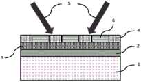
图1是传统干涉光刻光场照明特殊感光层材料示意图。Figure 1 is a schematic diagram of a special photosensitive layer material illuminated by a traditional interference lithography light field.
图2是特殊感光层材料形成振幅型掩模光栅示意图。Figure 2 is a schematic diagram of forming an amplitude mask grating with a special photosensitive layer material.
图3是第二次照明共振腔内介质层材料示意图。FIG. 3 is a schematic diagram of the material of the dielectric layer in the resonant cavity for the second illumination.
图4是共振腔内介质层材料形成第二次倍频图形的示意图。FIG. 4 is a schematic diagram of the second frequency doubling pattern formed by the dielectric layer material in the resonant cavity.
图5制备硅掩模或传递刻蚀其他功能材料的示意图。Figure 5 is a schematic diagram of preparing a silicon mask or transfer etching other functional materials.
图6实施例一中涉及的结构参数在光刻胶中获得的表面等离子体干涉光刻的COMSOL仿真图。FIG. 6 is a COMSOL simulation diagram of surface plasmon interference lithography obtained in the photoresist for the structural parameters involved in the first embodiment.
图7实施例二中以硅膜层和光刻胶掩蔽刻蚀层实现功能材料深刻蚀示意图。FIG. 7 is a schematic diagram of deep etching of functional materials by using a silicon film layer and a photoresist masking etching layer in the second embodiment.
图8实施例三中以硅膜层作为掩蔽层实现功能材料刻蚀示意图。FIG. 8 is a schematic diagram of implementing functional material etching using a silicon film layer as a masking layer in the third embodiment.
附图标记reference number
1、体硅材料;1. Bulk silicon material;
2、介质层;2. Dielectric layer;
3、金属层;3. Metal layer;
4、特殊感光材料;4. Special photosensitive materials;
5、传统干涉光刻照明光场;5. Traditional interference lithography illumination light field;
6、特殊感光材料发生透过率或/和折射率变化的部分;6. The part where the transmittance or/and the refractive index of the special photosensitive material change;
7、使共振腔体内介质层发生反应的第二次照明光场;7. The second illumination light field that makes the dielectric layer in the resonant cavity react;
8、功能性材料;8. Functional materials;
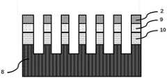
9、硅膜层;9. Silicon film layer;
10、光刻胶掩蔽刻蚀层。10. Photoresist masks the etching layer.
具体实施方式Detailed ways
下面结合附图以及具体实施方式进一步说明本发明。The present invention will be further described below with reference to the accompanying drawings and specific embodiments.
实施例一:Example 1:
本发明一种基于共振腔结构实现大面积超分辨光刻方法,具体步骤如下:The present invention is a method for realizing large-area super-resolution lithography based on a resonant cavity structure, and the specific steps are as follows:
步骤1、在体硅材料1上涂覆25nm的光刻胶。
步骤2、在光刻胶上蒸镀15nm的铝。
步骤3、在铝表面旋涂50nm厚度的水溶性重氮盐p-diazodiphenylamine chloridezinc chloride(DZS)膜层。经过步骤3后形成的器件结构如图1所示。
步骤4、选择441.6nm波长的He-Cd激光器产生的干涉光源照明步骤3获得的结构,使水溶性重氮盐感光,光强为10mW/cm2,照明时间为250s,形成220nm周期图形,如图2所示。
步骤5、将步骤4所得的结构放到中心波长为365nm,加偏振片后光强为25mW/cm2的紫外LED光源下,曝光时间为100s,将共振腔结构中的PHS光刻胶感光以获得表面等离子体干涉图形,如图3和图4所示。
步骤6、将特殊感光材料和铝层用3M胶带去掉后,用AR300-35显影液对PHS光刻胶显影,从而获得110nm周期的光刻胶图形。光刻效果仿真图如图6所示。
其中,图1是传统干涉光刻光场照明特殊感光层材料示意图。利用传统干涉光刻光场5照明特殊感光材料4;图2是特殊感光层材料形成振幅型掩模光栅示意图。特殊感光材料4在光场强度最大的区域透过率和/或折射率发生改变6。图3是第二次照明共振腔内介质层材料示意图。第二次照明光场7照明特殊感光材料形成的振幅型光栅4,透过金属层3使共振腔结构中的介质层2感光。图4是共振腔内介质层材料形成第二次倍频图形的示意图;图5制备硅掩模或传递刻蚀其他功能材料的示意图。用硅膜层9替代原有共振腔结构中的体硅材料1,以硅膜层9作为硬质掩蔽层,实现其他功能性材料8的传递刻蚀。图6实施例一中涉及的结构参数在光刻胶中获得的表面等离子体干涉光刻的COMSOL仿真图。掩模周期为220nm,在金属-介质-硅的共振腔体中实现了110nm周期的干涉光刻图形。Among them, FIG. 1 is a schematic diagram of a special photosensitive layer material illuminated by a traditional interference lithography light field. The special
实施例二:Embodiment 2:
本发明一种基于共振腔结构实现大面积超分辨光刻方法,具体步骤如下:The present invention is a method for realizing large-area super-resolution lithography based on a resonant cavity structure, and the specific steps are as follows:
步骤1、在石英基底上沉积50nm的金膜层。
步骤2、在金膜层上涂覆120nm厚的AR-3170光刻胶。
步骤3、将步骤2获得的结构在烘箱里用100℃烘0.5个小时。
步骤4、烘烤过的步骤2获得的结构放到磁控溅射中,沉积20nm厚的硅膜层。
步骤5、在步骤4获得的结构上涂覆25nm的光刻胶。
步骤6、在光刻胶上蒸镀15nm的铝。
步骤7、在铝表面旋涂50nm厚度的水溶性重氮盐p-diazodiphenylamine chloridezinc chloride(DZS)膜层。
步骤8、选择441.6nm波长的He-Cd激光器产生的干涉光源照明步骤7获得的结构,使水溶性重氮盐感光,光强为10mW/cm2,照明时间为250s,形成220nm周期图形。
步骤9、将步骤8所得的结构放到中心波长为365nm,加偏振片后光强为25mW/cm2的紫外LED光源下,曝光时间为100s,将共振腔结构中的PHS光刻胶感光以获得表面等离子体干涉图形。
步骤10、将特殊感光材料和铝层用3M胶带去掉后,用AR300-35显影液对PHS光刻胶显影,从而获得110nm周期的光刻胶图形。Step 10: After removing the special photosensitive material and the aluminum layer with 3M tape, develop the PHS photoresist with AR300-35 developer, so as to obtain a photoresist pattern with a period of 110 nm.
步骤11、以110nm周期的光刻胶图形为刻蚀掩蔽层利用反应离子刻蚀(RIE)传递刻蚀硅膜层。Step 11 , using a photoresist pattern with a period of 110 nm as an etching mask layer to transfer the silicon film layer by reactive ion etching (RIE).
步骤12、再以硅膜层为掩蔽刻蚀传递下层光刻胶AR-3170。Step 12, using the silicon film layer as a mask to etch and transfer the lower photoresist AR-3170.
步骤13、以下层光刻胶AR-3170图形为掩蔽层实现功能材料的刻蚀传递,刻蚀示意图如图7所示。Step 13 , the photoresist AR-3170 pattern of the following layer is used as a mask layer to realize the etching and transfer of the functional material, and the schematic diagram of the etching is shown in FIG. 7 .
步骤14、利用丙酮去除掉功能图形以上的结构,从而获得可用的功能结构。Step 14, using acetone to remove the structure above the functional figure, so as to obtain a usable functional structure.
图7实施例二中以硅膜层和光刻胶掩蔽刻蚀层实现功能材料深刻蚀示意图。介质层2中的光刻图形传递到硅膜层9上,再以硅膜层为掩蔽实现下层光刻胶10的传递,最后将图形传递到功能材料8上。FIG. 7 is a schematic diagram of deep etching of functional materials by using a silicon film layer and a photoresist masking etching layer in the second embodiment. The photolithography pattern in the
实施例三:Embodiment three:
本发明一种基于共振腔结构实现大面积超分辨光刻方法,具体步骤如下:The present invention is a method for realizing large-area super-resolution lithography based on a resonant cavity structure, and the specific steps are as follows:
步骤1、在石英基底上沉积50nm的银膜层。
步骤2、在银膜层上沉积20nm厚的硅膜层。
步骤3、在步骤2获得的结构上涂覆25nm的光刻胶。
步骤4、在光刻胶上蒸镀15nm的铝。
步骤5、在铝表面旋涂50nm厚度的水溶性重氮盐p-diazodiphenylamine chloridezinc chloride(DZS)膜层。
步骤6、选择441.6nm波长的He-Cd激光器产生的干涉光源照明步骤5获得的结构,使水溶性重氮盐感光,光强为10mW/cm2,照明时间为250s,形成220nm周期图形。
步骤7、将步骤6所得的结构放到中心波长为365nm,加偏振片后光强为25mW/cm2的紫外LED光源下,曝光时间为100s,将共振腔结构中的PHS光刻胶感光以获得表面等离子体干涉图形。
步骤8、将特殊感光材料和铝层用3M胶带去掉后,用AR300-35显影液对PHS光刻胶显影,从而获得110nm周期的光刻胶图形。
步骤9、以110nm周期的光刻胶图形为刻蚀掩蔽层利用反应离子刻蚀(RIE)传递刻蚀硅膜层。
步骤10、再以硅膜层为掩蔽RIE刻蚀传递功能材料,刻蚀示意图如图8所示。
步骤11、利用丙酮去除掉功能图形以上的结构,从而获得可用的功能结构。Step 11, using acetone to remove the structure above the functional figure, so as to obtain a usable functional structure.
图8实施例三中以硅膜层作为掩蔽层实现功能材料刻蚀示意图。介质层2中的光刻图形传递到硅膜层9上,再以硅膜层为掩蔽将图形传递到功能材料8上。FIG. 8 is a schematic diagram of implementing functional material etching using a silicon film layer as a masking layer in the third embodiment. The photolithographic pattern in the
Claims (3)
Translated fromChinesePriority Applications (1)
| Application Number | Priority Date | Filing Date | Title |
|---|---|---|---|
| CN201811510455.2ACN109669323B (en) | 2018-12-11 | 2018-12-11 | A method for realizing large-area super-resolution lithography based on resonant cavity structure |
Applications Claiming Priority (1)
| Application Number | Priority Date | Filing Date | Title |
|---|---|---|---|
| CN201811510455.2ACN109669323B (en) | 2018-12-11 | 2018-12-11 | A method for realizing large-area super-resolution lithography based on resonant cavity structure |
Publications (2)
| Publication Number | Publication Date |
|---|---|
| CN109669323A CN109669323A (en) | 2019-04-23 |
| CN109669323Btrue CN109669323B (en) | 2020-10-23 |
Family
ID=66143842
Family Applications (1)
| Application Number | Title | Priority Date | Filing Date |
|---|---|---|---|
| CN201811510455.2AActiveCN109669323B (en) | 2018-12-11 | 2018-12-11 | A method for realizing large-area super-resolution lithography based on resonant cavity structure |
Country Status (1)
| Country | Link |
|---|---|
| CN (1) | CN109669323B (en) |
Families Citing this family (4)
| Publication number | Priority date | Publication date | Assignee | Title |
|---|---|---|---|---|
| CN110989300A (en)* | 2020-01-02 | 2020-04-10 | 中国科学院上海光学精密机械研究所 | Super-resolution imaging photoetching system and method |
| US20240005064A1 (en)* | 2021-11-01 | 2024-01-04 | Institute of Microelectronics, Chinese Academy of Sciences | Method and apparatus for optimizing lithography quality, electronic device, medium and program product |
| CN114217510B (en)* | 2021-12-16 | 2022-09-20 | 中国科学院光电技术研究所 | Photoetching method |
| CN115826363A (en)* | 2022-10-17 | 2023-03-21 | 重庆大学 | Large-working-distance super-resolution photoetching device based on photonic crystal with defects and method thereof |
Citations (3)
| Publication number | Priority date | Publication date | Assignee | Title |
|---|---|---|---|---|
| JPS5643620A (en)* | 1979-09-17 | 1981-04-22 | Mitsubishi Electric Corp | Production of blazed grating |
| US6528238B1 (en)* | 2000-09-22 | 2003-03-04 | David Seniuk | Methods for making patterns in radiation sensitive polymers |
| CN103499913A (en)* | 2013-10-20 | 2014-01-08 | 安徽师范大学 | Surface plasmon imaging photoetching structure |
Family Cites Families (3)
| Publication number | Priority date | Publication date | Assignee | Title |
|---|---|---|---|---|
| JPH02127645A (en)* | 1988-11-08 | 1990-05-16 | Fujitsu Ltd | How to form a positive pattern |
| CN101441421B (en)* | 2008-12-04 | 2010-10-20 | 中国科学院光电技术研究所 | A Device for Realizing Maskless Surface Plasmon Interference Lithography Using a Laue Mirror |
| CN101846880B (en)* | 2010-05-12 | 2012-05-30 | 上海交通大学 | Nano photoetching method for exciting surface plasma |
- 2018
- 2018-12-11CNCN201811510455.2Apatent/CN109669323B/enactiveActive
Patent Citations (3)
| Publication number | Priority date | Publication date | Assignee | Title |
|---|---|---|---|---|
| JPS5643620A (en)* | 1979-09-17 | 1981-04-22 | Mitsubishi Electric Corp | Production of blazed grating |
| US6528238B1 (en)* | 2000-09-22 | 2003-03-04 | David Seniuk | Methods for making patterns in radiation sensitive polymers |
| CN103499913A (en)* | 2013-10-20 | 2014-01-08 | 安徽师范大学 | Surface plasmon imaging photoetching structure |
Also Published As
| Publication number | Publication date |
|---|---|
| CN109669323A (en) | 2019-04-23 |
Similar Documents
| Publication | Publication Date | Title |
|---|---|---|
| CN109669323B (en) | A method for realizing large-area super-resolution lithography based on resonant cavity structure | |
| US9116430B2 (en) | Plasmonic lithography using phase mask | |
| Alkaisi et al. | Nanolithography in the evanescent near field | |
| US20120224159A1 (en) | Method and apparatus for patterning a disk | |
| JP6127203B2 (en) | Super-resolution imaging lithography | |
| CN102053491B (en) | Ultra-deep subwavelength tunable nano photoetching structure and method based on surface plasma resonant cavity | |
| Wong et al. | High throughput and high yield nanofabrication of precisely designed gold nanohole arrays for fluorescence enhanced detection of biomarkers | |
| WO2011108259A1 (en) | Process for production of photoresist pattern | |
| CN101441411A (en) | Surface plasma resonance exposure photolithography method | |
| CN105549336A (en) | Nano photoetching device and method for preparing super diffraction limit pattern | |
| CN115047728B (en) | Imaging structure protection method and structure for plasma resonant cavity lens photoetching | |
| WO2019114359A1 (en) | Negative-refraction imaging photolithography method and apparatus | |
| US20120156594A1 (en) | Photomask including super lens and manufacturing method thereof | |
| KR101875771B1 (en) | Mask for photolithography, manufacturing method thereof and manufacturing method of substrate using the mask | |
| CN109116687B (en) | A light-generating device for super-resolution lithography | |
| CN101726998A (en) | A method for improving the quality of surface plasmon lithography by using metal reflective film structure | |
| CN101846880B (en) | Nano photoetching method for exciting surface plasma | |
| CN101587296A (en) | Surface plasma nano photolithography | |
| Skinner et al. | Large-area subwavelength aperture arrays fabricated using nanoimprint lithography | |
| CN117492330A (en) | A surface plasmon lithography imaging structure | |
| CN117742086A (en) | A plasma interference lithography structure | |
| Romanato et al. | Interferential lithography of 1D thin metallic sinusoidal gratings: accurate control of the profile for azimuthal angular dependent plasmonic effects and applications | |
| CN109283788B (en) | Nano-pattern processing system and method for rotary near-field photoetching | |
| Yoshifuji et al. | Fabrication of high-aspect-ratio transmission grating using DDR process for 10 nm EUV resist evaluation by EUV interference lithography | |
| CN109901362A (en) | Secondary imaging optical lithography method and apparatus |
Legal Events
| Date | Code | Title | Description |
|---|---|---|---|
| PB01 | Publication | ||
| PB01 | Publication | ||
| SE01 | Entry into force of request for substantive examination | ||
| SE01 | Entry into force of request for substantive examination | ||
| GR01 | Patent grant | ||
| GR01 | Patent grant |