CN109634900B - A multi-level low-latency interconnect structure based on AXI protocol - Google Patents
A multi-level low-latency interconnect structure based on AXI protocolDownload PDFInfo
- Publication number
- CN109634900B CN109634900BCN201811347593.3ACN201811347593ACN109634900BCN 109634900 BCN109634900 BCN 109634900BCN 201811347593 ACN201811347593 ACN 201811347593ACN 109634900 BCN109634900 BCN 109634900B
- Authority
- CN
- China
- Prior art keywords
- bus
- axi
- master
- slave
- protocol
- Prior art date
- Legal status (The legal status is an assumption and is not a legal conclusion. Google has not performed a legal analysis and makes no representation as to the accuracy of the status listed.)
- Active
Links
Images


Classifications
- G—PHYSICS
- G06—COMPUTING OR CALCULATING; COUNTING
- G06F—ELECTRIC DIGITAL DATA PROCESSING
- G06F13/00—Interconnection of, or transfer of information or other signals between, memories, input/output devices or central processing units
- G06F13/38—Information transfer, e.g. on bus
- G06F13/42—Bus transfer protocol, e.g. handshake; Synchronisation
- G06F13/4204—Bus transfer protocol, e.g. handshake; Synchronisation on a parallel bus
- G06F13/4221—Bus transfer protocol, e.g. handshake; Synchronisation on a parallel bus being an input/output bus, e.g. ISA bus, EISA bus, PCI bus, SCSI bus
- G06F13/423—Bus transfer protocol, e.g. handshake; Synchronisation on a parallel bus being an input/output bus, e.g. ISA bus, EISA bus, PCI bus, SCSI bus with synchronous protocol
Landscapes
- Engineering & Computer Science (AREA)
- Theoretical Computer Science (AREA)
- Physics & Mathematics (AREA)
- General Engineering & Computer Science (AREA)
- General Physics & Mathematics (AREA)
- Bus Control (AREA)
Abstract
Translated fromChinese
Description
Translated fromChinese技术领域technical field
本发明涉及一种互连结构,特别是一种基于AXI协议的多层次低延迟互连结构,属于集成电路多核互连架构设计领域。The invention relates to an interconnection structure, in particular to a multi-level low-latency interconnection structure based on an AXI protocol, and belongs to the field of integrated circuit multi-core interconnection architecture design.
背景技术Background technique
随着集成电路技术的不断发展,为了达到更高的处理性能和效率,多核处理器已经成为主流设计。多核处理器的设计以IP核复用技术为基础,因此IP核以何种方法互连越来越影响处理器的数据吞吐率等性能指标。目前国际上有多种IP核互连规范,包括IBM的CoreConnect总线、ARM的AMBA(Advanced Microcontroller Bus Architecture)、SilicoreCorp的Wishbone、Altera的Avalon总线以及MIPS的ECTM Interface等。With the continuous development of integrated circuit technology, in order to achieve higher processing performance and efficiency, multi-core processors have become mainstream designs. The design of the multi-core processor is based on the IP core multiplexing technology, so the way the IP cores are interconnected increasingly affects the performance indicators such as the data throughput rate of the processor. At present, there are a variety of IP core interconnection specifications in the world, including IBM's CoreConnect bus, ARM's AMBA (Advanced Microcontroller Bus Architecture), SilicoreCorp's Wishbone, Altera's Avalon bus, and MIPS' ECTM Interface.
其中AXI是ARM推出的AMBA 3.0总线协议中最重要的部分,是一种面向高性能、高带宽、低延迟的片内总线。AXI传输协议包含五条通道,分别是读地址通道、读数据通道、写地址通道、写数据通道和写响应通道,并且这些通道都是单向通道。读写交易拥有其对应的读写地址通道,地址通道作为一次交易所需的地址和控制信息的载体。一次突发读或写操作可以包含一次或者多次传输。每条通道都有对应的VALID和READY信号,构成了通道内的握手关系,用以传输数据及控制信息,双向的流控制机制使得主从设备能够操控数据和控制信息的流动和切断。AXI协议是基于突发传输方式的,主设备发送第一拍传输的首地址和控制信息,之后不再发送后面的数据对应的地址,即一个地址对应一串数据。该协议拥有独特的优势,包括分离的读写通信通道、独立的地址/控制和数据段、支持非对齐传输和OUTSTANDING传输,更加容易进行时序收敛等,其技术丰富了现有的AMBA标准内容,满足超高性能和复杂处理器设计需求,已经被广泛应用于多核处理器的设计中。Among them, AXI is the most important part of the AMBA 3.0 bus protocol introduced by ARM. It is an on-chip bus for high performance, high bandwidth and low delay. The AXI transmission protocol contains five channels, namely read address channel, read data channel, write address channel, write data channel and write response channel, and these channels are all unidirectional channels. The read-write transaction has its corresponding read-write address channel, and the address channel serves as the carrier of the address and control information required for a transaction. A burst read or write operation can consist of one or more transfers. Each channel has corresponding VALID and READY signals, which constitute a handshake relationship within the channel to transmit data and control information. The bidirectional flow control mechanism enables the master and slave devices to control the flow and cutoff of data and control information. The AXI protocol is based on the burst transmission mode. The master device sends the first address and control information of the first transmission, and then does not send the address corresponding to the following data, that is, an address corresponds to a string of data. The protocol has unique advantages, including separate read and write communication channels, independent address/control and data segments, support for unaligned transmission and OUTSTANDING transmission, easier timing closure, etc. Its technology enriches the existing AMBA standard content, To meet the requirements of ultra-high performance and complex processor design, it has been widely used in the design of multi-core processors.
在复杂多核处理器的设计过程中会涉及到核与核之间、核与加速单元之间、核与外设之间等多个模块间的互连通信,涉及到数据一致性和互连总线数据吞吐率低等一系列问题。所以有必要在低延迟总线设计方面进行改进,提高数据吞吐率的同时兼顾可靠性及功耗等性能要求。In the design process of complex multi-core processors, it will involve interconnection and communication between multiple modules, such as between cores, between cores and acceleration units, between cores and peripherals, etc., involving data consistency and interconnection bus. A series of problems such as low data throughput. Therefore, it is necessary to improve the low-latency bus design to improve data throughput while taking into account performance requirements such as reliability and power consumption.
发明内容SUMMARY OF THE INVENTION
本发明的目的在于克服现有技术的不足,提出一种基于AXI协议的多层次低延迟互连结构,增加了数据传输的并行度,降低了传输延迟,有效提高了数据吞吐率,同时兼顾了传输可靠性等性能要求。The purpose of the present invention is to overcome the deficiencies of the prior art, and propose a multi-level low-latency interconnection structure based on the AXI protocol, which increases the parallelism of data transmission, reduces the transmission delay, effectively improves the data throughput rate, and takes into account both the Performance requirements such as transmission reliability.
本发明目的通过如下技术方案予以实现:The object of the present invention is achieved through the following technical solutions:
提供一种基于AXI协议的多层次低延迟互连结构,核间总线互连单元和片上总线互连单元,核间总线互连单元用于多个处理器核之间的数据通讯;片上总线互连单元用于多个外部设备之间以及处理器核与外部设备之间的数据通讯。A multi-level low-latency interconnect structure based on AXI protocol is provided, an inter-core bus interconnect unit and an on-chip bus interconnect unit, the inter-core bus interconnect unit is used for data communication between multiple processor cores; the on-chip bus interconnect unit is provided. The connection unit is used for data communication between a plurality of external devices and between the processor core and the external devices.
优选的,核间总线互连单元多个主/从接口以及虚拟通道转换开关,主/从接口分别用于连接处理器核,虚拟通道转换开关基于识别码配置各处理器核之间的通讯通路。Preferably, the inter-core bus interconnection unit has multiple master/slave interfaces and virtual channel switches, the master/slave interfaces are respectively used to connect the processor cores, and the virtual channel switch configures the communication paths between the processor cores based on the identification code .
优选的,虚拟通道转换开关包括处理器的识别码分配器、可配置互联通道;识别码分配器用于给多个处理器核Core分配识别码,多个处理器核Core基于分配识别码相互识别;可配置互联通道基于识别码配置处理器核之间的连接通道,使得配置处理器核之间能够进行相互通讯。Preferably, the virtual channel switch includes a processor identification code distributor and a configurable interconnection channel; the identification code distributor is used to assign identification codes to multiple processor cores, and the multiple processor cores identify each other based on the assigned identification codes; The configurable interconnection channel configures the connection channel between the processor cores based on the identification code, so that the configuration processor cores can communicate with each other.
优选的,片上总线互连单元包括多层次互连结构、主设备接口、从设备接口以及多个转换桥;主设备接口用于连接从设备,从设备接口用于连接主设备;转换桥用于多种总线协议之间的转换;多层次互连结构用于主从设备之间的连接通讯。Preferably, the on-chip bus interconnection unit includes a multi-level interconnection structure, a master device interface, a slave device interface and a plurality of conversion bridges; the master device interface is used to connect the slave device, and the slave device interface is used to connect to the master device; the conversion bridge is used for Conversion between multiple bus protocols; multi-level interconnection structure is used for connection communication between master and slave devices.
优选的,多层次互连结构包括AXI总线矩阵开关和AHB总线开关,AXI总线矩阵开关通过AXI主设备接口连接AXI从设备,通过AXI从设备接口连接主设备;AHB总线开关通过AHB主设备接口连接AHB从设备,通过AHB从设备接口连接AHB主设备。Preferably, the multi-level interconnection structure includes an AXI bus matrix switch and an AHB bus switch, the AXI bus matrix switch is connected to the AXI slave device through the AXI master device interface, and the AXI slave device interface is connected to the master device; the AHB bus switch is connected through the AHB master device interface. The AHB slave device is connected to the AHB master device through the AHB slave device interface.
优选的,多个转换桥包括AHBLite2AXI转换桥、AXI2AXI转换桥、AXI2AHB转换桥、AHB2APB转换桥;AHBLite2AXI转换桥通过从设备接口连接AXI总线矩阵开关,用于AHBLite总线协议与AXI总线协议的转换;AXI2AXI转换桥通过从设备接口连接AXI总线矩阵开关,通过主设备接口连接低延迟核间总线互连单元BMCNI,用于BMCNI与AXI总线矩阵开关的通讯连接;AXI2AHB转换桥通过主设备接口连接AXI总线矩阵开关,通过从设备接口连接AHB总线开关,用于AXI总线协议与AHB总线协议的转换;AHB2APB转换桥通过主设备接口连接AHB总线开关,用于AHB总线协议与APB总线协议的转换。Preferably, the plurality of conversion bridges include AHBLite2AXI conversion bridge, AXI2AXI conversion bridge, AXI2AHB conversion bridge, AHB2APB conversion bridge; AHBLite2AXI conversion bridge is connected to the AXI bus matrix switch through the slave device interface for conversion between AHBLite bus protocol and AXI bus protocol; AXI2AXI The conversion bridge is connected to the AXI bus matrix switch through the slave device interface, and the low-latency inter-core bus interconnection unit BMCNI is connected through the master device interface, which is used for the communication connection between BMCNI and the AXI bus matrix switch; the AXI2AHB conversion bridge is connected to the AXI bus matrix through the master device interface. The switch is connected to the AHB bus switch through the slave device interface, which is used for the conversion of the AXI bus protocol and the AHB bus protocol; the AHB2APB conversion bridge is connected to the AHB bus switch through the master device interface, which is used for the conversion of the AHB bus protocol and the APB bus protocol.
优选的,核间总线互连单元作为主设备连接到AXI总线矩阵开关。Preferably, the inter-core bus interconnection unit is connected to the AXI bus matrix switch as a master device.
优选的,AXI总线矩阵开关包括虚拟通道和多个缓存,通讯频率高于阈值的主从设备,其接口连接虚拟缓存,主从设备之间加入虚拟通道,虚拟通道具有可配置节点,通过配置可配置节点建立通讯通道。Preferably, the AXI bus matrix switch includes a virtual channel and a plurality of buffers, the master-slave device whose communication frequency is higher than the threshold value, its interface is connected to the virtual buffer, the virtual channel is added between the master-slave device, and the virtual channel has configurable nodes. Configure the node to establish a communication channel.
优选的,从设备对读取的数据包中添加VALID信号,标识通道上的数据合法和控制信息可用,主设备使用READY信号标识准备好接收数据,如果VALID信号有效则接收该数据;LAST信号标识读操作中的最后一个数据传输。Preferably, a VALID signal is added to the data packet read by the slave device to identify that the data on the channel is legal and control information is available, the master device uses the READY signal to identify that it is ready to receive data, and receives the data if the VALID signal is valid; the LAST signal identifies The last data transfer in a read operation.
优选的,写数据通道实现主设备向从设备传输写数据,写数据包中包含STROBE信号,标识数据包中哪个字节有效;从设备利用写响应通道返回响应,每个写交易结束都返回完成信号DONE;最后一个突发传输信号后返回一个LAST信号。Preferably, the write data channel enables the master device to transmit write data to the slave device, and the write data packet contains a STROBE signal to identify which byte in the data packet is valid; the slave device uses the write response channel to return a response, and the completion of each write transaction is returned. Signal DONE; returns a LAST signal after the last burst transfer signal.
优选的,还包括定时器,从总线脱离空闲态开始计时,到总线完成一次传输任务计时结束,如果在规定的超时时限内总线仍没有响应请求,则认为总线已经处于死锁无响应状态。Preferably, it also includes a timer, which starts from the time when the bus leaves the idle state and ends when the bus completes a transmission task. If the bus still does not respond to the request within the specified timeout period, it is considered that the bus is in a deadlock and no response state.
本发明与现有技术相比具有如下优点:Compared with the prior art, the present invention has the following advantages:
(1)本发明提出了一种多层次低延迟互连结构,同时考虑了多核之间及核与外设之间的高吞吐低延迟数据传输,根据数据传输的不同特点设计了多层次的互连结构,分别建立了高吞吐核间总线互连结构,保证了处理器核之间的高吞吐通讯,建立低延迟片上总线互连结构,保证了数据传输的可靠性和高效率。(1) The present invention proposes a multi-level low-latency interconnection structure, and considers high-throughput and low-latency data transmission between multiple cores and between cores and peripherals, and designs a multi-level interconnection structure according to different characteristics of data transmission. A high-throughput inter-core bus interconnection structure is established respectively to ensure high-throughput communication between processor cores, and a low-latency on-chip bus interconnection structure is established to ensure the reliability and high efficiency of data transmission.
(2)本发明提出了一种高吞吐低延迟核间互连结构,基于AXI协议,增加了虚拟通道转换开关设计,能够快速建立核与核之间的连接,保证处理器核之间高效通信,利用虚拟通道设计增加了传输带宽,减小了传输延时,提高了核间总线互连单元的性能。(2) The present invention proposes a high-throughput and low-latency inter-core interconnection structure. Based on the AXI protocol, a virtual channel switch design is added, which can quickly establish the connection between cores and ensure efficient communication between processor cores. , using the virtual channel design to increase the transmission bandwidth, reduce the transmission delay, and improve the performance of the inter-core bus interconnection unit.
(3)本发明提出了一种多层次并行复用片上总线互连结构,利用虚拟通道技术,可以通过将主设备的冲突请求分配到不同的虚拟通道中,可以提高数据传输的有效带宽。(3) The present invention proposes a multi-level parallel multiplexing on-chip bus interconnection structure. Using the virtual channel technology, the conflict request of the master device can be allocated to different virtual channels, which can improve the effective bandwidth of data transmission.
(4)本发明在互连结构中增加超时检测机制,通过合理的设置超时时限,既保证了数据正确的传输,提高了互连结构的可靠性,又可以通过设置超时时限,很好的兼顾总线的传输性能。(4) The present invention adds a timeout detection mechanism in the interconnection structure, and by reasonably setting the timeout time limit, not only the correct transmission of data is ensured, the reliability of the interconnection structure is improved, but also by setting the timeout limit, a good balance can be achieved. The transfer performance of the bus.
附图说明Description of drawings
图1是本发明多层次低延迟互连结构结构图;Fig. 1 is the structure diagram of multi-level low-delay interconnection structure of the present invention;
图2是本发明高吞吐低延迟核间总线互连单元结构图;Fig. 2 is the high-throughput low-latency inter-core bus interconnection unit structural diagram of the present invention;
图3是本发明多层次并行复用片上总线互连单元读通道结构图;3 is a multi-level parallel multiplexing on-chip bus interconnection unit read channel structure diagram of the present invention;
图4是本发明多层次并行复用片上总线互连单元写通道结构图;4 is a multi-level parallel multiplexing on-chip bus interconnection unit write channel structure diagram of the present invention;
图5是本发明多层次并行复用片上总线互连单元虚拟通道示意图。5 is a schematic diagram of a virtual channel of a multi-level parallel multiplexing on-chip bus interconnection unit of the present invention.
具体实施方式Detailed ways
下面结合附图对本发明作进一步描述。The present invention will be further described below in conjunction with the accompanying drawings.
如图1所示,本发明多层次低延迟互连结构,主要由高吞吐低延迟核间总线互连单元BMCNI和多层次并行复用片上总线互连单元BMSNI两个部分组成;多层次低延迟互连结构BMNI包括AMBA多层次互连结构、AMBA从设备接口、AMBA主设备接口以及多个转换桥。As shown in Figure 1, the multi-level low-latency interconnection structure of the present invention is mainly composed of two parts: a high-throughput and low-latency inter-core bus interconnection unit BMCNI and a multi-level parallel multiplexing on-chip bus interconnection unit BMSNI; The interconnection structure BNI includes AMBA multi-level interconnection structure, AMBA slave device interface, AMBA master device interface and multiple switching bridges.
AMBA多层次互连结构包括AXI总线矩阵开关、AHB总线开关;AXI总线矩阵开关用于连接AXI主设备与AXI从设备,建立AXI主设备与AXI从设备之间的高效通讯,通过AXI主设备接口连接AXI从设备,通过AXI从设备接口连接AXI主设备;AHB总线开关用于连接AHB主设备与AHB从设备,建立AHB主设备与AHB从设备之间的高效通讯,通过AHB主设备接口连接AHB从设备,通过AHB从设备接口连接AHB主设备。AMBA multi-level interconnection structure includes AXI bus matrix switch, AHB bus switch; AXI bus matrix switch is used to connect AXI master device and AXI slave device, establish efficient communication between AXI master device and AXI slave device, through the AXI master device interface Connect the AXI slave device, and connect the AXI master device through the AXI slave device interface; the AHB bus switch is used to connect the AHB master device and the AHB slave device, establish efficient communication between the AHB master device and the AHB slave device, and connect the AHB through the AHB master device interface. The slave device connects to the AHB master device through the AHB slave device interface.
AMBA从设备接口、AMBA主设备接口用于连接主从设备。The AMBA slave device interface and the AMBA master device interface are used to connect the master and slave devices.
多个转换桥包括AHBLite2AXI转换桥、AXI2AXI转换桥、AXI2AHB转换桥、AHB2APB转换桥;AHBLite2AXI转换桥通过从设备接口连接AXI总线矩阵开关,用于AHBLite总线协议与AXI总线协议的转换;AXI2AXI转换桥通过从设备接口连接AXI总线矩阵开关,通过主设备接口连接低延迟核间总线互连单元BMCNI,用于BMCNI与AXI总线矩阵开关的通讯;AXI2AHB转换桥通过主设备接口连接AXI总线矩阵开关,通过从设备接口连接AHB总线开关,用于AXI总线协议与AHB总线协议的转换;AHB2APB转换桥通过主设备接口连接AHB总线开关,用于AHB总线协议与APB总线协议的转换。Multiple conversion bridges include AHBLite2AXI conversion bridge, AXI2AXI conversion bridge, AXI2AHB conversion bridge, AHB2APB conversion bridge; AHBLite2AXI conversion bridge connects AXI bus matrix switch through slave device interface, which is used for AHBLite bus protocol and AXI bus protocol conversion; AXI2AXI conversion bridge through The slave device interface is connected to the AXI bus matrix switch, and the low-latency inter-core bus interconnection unit BMCNI is connected through the master device interface, which is used for the communication between BMCNI and the AXI bus matrix switch; the AXI2AHB conversion bridge is connected to the AXI bus matrix switch through the master device interface. The device interface is connected to the AHB bus switch for the conversion of the AXI bus protocol and the AHB bus protocol; the AHB2APB conversion bridge is connected to the AHB bus switch through the main device interface for the conversion of the AHB bus protocol and the APB bus protocol.
如图2所示,本发明中高吞吐低延迟核间总线互连单元BMCNI,主要负责多核间数据高可靠通信。包括四个主/从接口、虚拟通道转换开关;四个主/从接口结构相同,分别用于连接处理器核Core,核间总线基于AXI总线;虚拟通道转换开关包括处理器的识别码分配器、可配置互联通道,识别码分配器用于给多个处理器核Core分配识别码,多个处理器核Core基于分配识别码相互识别;可配置互联通道基于识别码配置处理器核Core之间的连接通道,使得配置处理器核Core之间能够进行相互通讯。虚拟通道转换开关最大用途就是能够很快的建立核与核之间的直接通信,保证处理器内核之间快速建立连接,利用虚拟通道的设计增加有效传输带宽,减小传输延时,提高总线性能。在该总线互连结构中,关键技术在于虚拟通道转换开关(SWITCH-VP)的设计,其主要作用是能够合理的分配多核之间的数据访问。该互连结构为了满足多个核之间互相访问的需要,提出了虚拟多通道概念,所谓虚拟通道就是多个设备通过缓存连接在同一条总线上,并且为每个接口分配缓存,两个缓存之间由一条实际物理总线通道连接,采用地址共享数据复用的方式,该总线可以被多条逻辑链路复用,且逻辑链路可以独立使用各自的缓存空间。As shown in FIG. 2 , the high-throughput and low-latency inter-core bus interconnection unit BMCNI in the present invention is mainly responsible for highly reliable communication of data between multiple cores. It includes four master/slave interfaces and virtual channel changeover switches; the four master/slave interfaces have the same structure and are respectively used to connect to the processor core, and the inter-core bus is based on AXI bus; the virtual channel changeover switch includes the identification code distributor of the processor , Configurable interconnection channel, the identification code distributor is used to assign identification codes to multiple processor cores, and multiple processor cores identify each other based on the assigned identification codes; the configurable interconnection channel configures the communication between the processor cores based on the identification code. The connection channel enables mutual communication between the configured processor cores. The biggest use of the virtual channel switch is to quickly establish direct communication between cores, to ensure the rapid establishment of connections between processor cores, and to use the design of virtual channels to increase effective transmission bandwidth, reduce transmission delay, and improve bus performance. . In the bus interconnect structure, the key technology lies in the design of the virtual channel switch (SWITCH-VP), whose main function is to reasonably allocate data access between multiple cores. In order to meet the needs of mutual access between multiple cores, the interconnection structure proposes the concept of virtual multi-channel. The so-called virtual channel is that multiple devices are connected to the same bus through the cache, and each interface is allocated a cache, two caches It is connected by an actual physical bus channel, and adopts the method of address sharing and data multiplexing. The bus can be multiplexed by multiple logical links, and the logical links can use their own buffer space independently.
如图3所示为本发明中多层次并行复用片上总线互连单元中读通道结构图。从设备对读取的数据包中添加VALID信号,标识通道上的数据合法和控制信息可用,主设备使用READY信号判定是否准备好接收数据,可以接收从设备的数据包,如果VALID信号有效则接收该数据。读操作和写操作都含有一个LAST信号标识一次交易中的最后一个数据传输。读和写都有各自的地址通道。读数据通道用于传输从设备返回给主设备的读数据和读响应信息。读数据通道包含数据总线,宽度为64Bits,读响应标志着读交易完成。FIG. 3 is a structural diagram of a read channel in a multi-level parallel multiplexing on-chip bus interconnection unit in the present invention. The slave device adds a VALID signal to the read data packet to identify the validity of the data on the channel and the availability of control information. The master device uses the READY signal to determine whether it is ready to receive data, and can receive data packets from the slave device. If the VALID signal is valid, receive the data. Both read and write operations contain a LAST signal to identify the last data transfer in a transaction. Read and write have their own address channel. The read data channel is used to transmit read data and read response information returned from the slave device to the master device. The read data channel includes a data bus with a width of 64Bits, and the read response marks the completion of the read transaction.
如图4所示为本发明中多层次并行复用片上总线互连单元中写通道结构图。写数据通道负责主设备向从设备传输写数据,包含了和读数据通道相同的位宽数据总线,写数据包中包含STROBE信号,标识数据包中哪个字节有效,从设备利用STROBE信号来判断总线上哪个字节是有效的。通过对数据通道信息添加缓冲器可以让主设备在没有获得从设备前一个写交易确认的情况下继续进行新的写交易。从设备利用写响应通道返回响应,所有的写交易结束都返回完成信号DONE。基于突发传输BURST,不是每拍都返回一个完成信号,而是每个突发传输BURST完成后一起返回一个完成信号。最后一个突发传输BURST返回一个LAST信号。FIG. 4 is a structure diagram of the write channel in the multi-level parallel multiplexing on-chip bus interconnection unit in the present invention. The write data channel is responsible for transmitting write data from the master device to the slave device. It contains the same bit-width data bus as the read data channel. The write data packet contains the STROBE signal, which identifies which byte in the data packet is valid. The slave device uses the STROBE signal to judge. Which byte on the bus is valid. By adding buffers to the data channel information, the master device can continue to perform new write transactions without obtaining confirmation of the previous write transaction from the slave device. The slave device uses the write response channel to return a response, and all write transactions end with a completion signal DONE. Based on the burst transmission BURST, instead of returning a completion signal every beat, a completion signal is returned together after each burst transmission BURST is completed. The last burst transfer BURST returns a LAST signal.
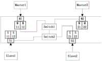
如图5所示为本发明中多层次并行复用片上总线互连单元中虚拟通道示意图。AXI总线矩阵开关包括虚拟通道,在通讯频率高于阈值的主从设备之间加入虚拟通道,虚拟通道中间具有可配置节点,建立设备之间的通道,该主从设备接口连接虚拟缓存(M11、M12、M21、M22、S11、S12、S21、S22),用于数据的缓存,使得能够同时存储两路数据,提高了设备的数据传输效率。图5中主设备Master1(简称M1)和Master2(简称M2),从设备Slave1(简称S1)和Slave2(简称S2),当M1对S1发起操作请求,M2对S2也同时发起操作请求时,可以有效的利用地址共享数据复用的方式提高数据传输的并行度,提高总线互连结构的有效数据传输带宽。FIG. 5 is a schematic diagram of a virtual channel in the multi-level parallel multiplexing on-chip bus interconnection unit in the present invention. The AXI bus matrix switch includes a virtual channel, and a virtual channel is added between the master and slave devices whose communication frequency is higher than the threshold. There are configurable nodes in the middle of the virtual channel to establish a channel between devices. The master and slave device interfaces are connected to the virtual cache (M11, M12, M21, M22, S11, S12, S21, S22), used for data buffering, so that two channels of data can be stored at the same time, and the data transmission efficiency of the device is improved. In Figure 5, the master devices Master1 (M1 for short) and Master2 (M2 for short), and the slave devices Slave1 (S1 for short) and Slave2 (S2 for short), when M1 initiates an operation request to S1, and M2 also initiates an operation request to S2 at the same time, you can Effective use of the address sharing data multiplexing method improves the parallelism of data transmission and improves the effective data transmission bandwidth of the bus interconnection structure.
本发明加入了超时检测机制,从总线脱离空闲态开始计时,到总线完成一次传输任务计时结束,如果在规定的超时时限内总线仍没有响应请求,则强制认为总线已经处于死锁无响应状态,此时总线给请求方返回一个应答信号,告诉主设备此次操作没有响应,总线死锁。主设备在接收到总线的应答信号后可以选择重新发出操作请求或者放弃此次操作。总线发送完应答信号之后开始进入空闲态。此时总线释放,主从设备通信状态恢复,重新开始新的请求、仲裁。The present invention adds a timeout detection mechanism, which starts timing from the time the bus leaves the idle state, and ends when the bus completes a transmission task. If the bus still does not respond to the request within the specified timeout period, the bus is forcibly considered to be in a deadlock and no response state. At this time, the bus returns a response signal to the requester, telling the master device that there is no response to this operation, and the bus is deadlocked. After receiving the response signal from the bus, the master device can choose to re-send the operation request or give up the operation. The bus starts to enter the idle state after sending the response signal. At this time, the bus is released, the communication status of the master and slave devices is restored, and new requests and arbitrations are restarted.
以上所述,仅为本发明最佳的具体实施方式,但本发明的保护范围并不局限于此,任何熟悉本技术领域的技术人员在本发明揭露的技术范围内,可轻易想到的变化或替换,都应涵盖在本发明的保护范围之内。The above is only the best specific embodiment of the present invention, but the protection scope of the present invention is not limited to this. Substitutions should be covered within the protection scope of the present invention.
本发明说明书中未作详细描述的内容属于本领域专业技术人员的公知技术。Contents that are not described in detail in the specification of the present invention belong to the well-known technology of those skilled in the art.
Claims (5)
Priority Applications (1)
| Application Number | Priority Date | Filing Date | Title |
|---|---|---|---|
| CN201811347593.3ACN109634900B (en) | 2018-11-13 | 2018-11-13 | A multi-level low-latency interconnect structure based on AXI protocol |
Applications Claiming Priority (1)
| Application Number | Priority Date | Filing Date | Title |
|---|---|---|---|
| CN201811347593.3ACN109634900B (en) | 2018-11-13 | 2018-11-13 | A multi-level low-latency interconnect structure based on AXI protocol |
Publications (2)
| Publication Number | Publication Date |
|---|---|
| CN109634900A CN109634900A (en) | 2019-04-16 |
| CN109634900Btrue CN109634900B (en) | 2020-12-08 |
Family
ID=66067917
Family Applications (1)
| Application Number | Title | Priority Date | Filing Date |
|---|---|---|---|
| CN201811347593.3AActiveCN109634900B (en) | 2018-11-13 | 2018-11-13 | A multi-level low-latency interconnect structure based on AXI protocol |
Country Status (1)
| Country | Link |
|---|---|
| CN (1) | CN109634900B (en) |
Families Citing this family (8)
| Publication number | Priority date | Publication date | Assignee | Title |
|---|---|---|---|---|
| CN110674075B (en)* | 2019-09-27 | 2023-03-10 | 山东华芯半导体有限公司 | Method and system for realizing AXI bus broadcasting mechanism |
| CN111538688B (en)* | 2020-05-26 | 2021-11-16 | 北京爱芯科技有限公司 | Data processing method, device, module and chip |
| CN113434460B (en)* | 2021-08-26 | 2022-01-11 | 长沙海格北斗信息技术有限公司 | Multi-bus topology system in SoC (System on chip) architecture and bus interconnection method |
| CN115412394B (en)* | 2022-08-22 | 2023-08-18 | 奥特酷智能科技(南京)有限公司 | Heterogeneous domain controller inter-core communication method based on AutoSar |
| CN116016698B (en)* | 2022-12-01 | 2024-04-05 | 电子科技大学 | A peer-to-peer interface and data interaction method for RapidIO controller and interconnect bare core |
| CN116795763B (en)* | 2023-07-31 | 2023-11-21 | 摩尔线程智能科技(北京)有限责任公司 | Method, system on chip and chip for data packet transmission based on AXI protocol |
| CN118363904B (en)* | 2024-06-18 | 2024-12-06 | 无锡芯光互连技术研究院有限公司 | TileLink bus to APB bus conversion method and chip |
| CN118568035B (en)* | 2024-07-31 | 2024-11-12 | 苏州旗芯微半导体有限公司 | Embedded Systems |
Family Cites Families (7)
| Publication number | Priority date | Publication date | Assignee | Title |
|---|---|---|---|---|
| CN101169771B (en)* | 2007-11-30 | 2010-06-02 | 华为技术有限公司 | A kind of external interface device of AXI internal bus and data transmission method thereof |
| US8798038B2 (en)* | 2011-08-26 | 2014-08-05 | Sonics, Inc. | Efficient header generation in packetized protocols for flexible system on chip architectures |
| CN103345461B (en)* | 2013-04-27 | 2016-01-20 | 电子科技大学 | Based on the polycaryon processor network-on-a-chip with accelerator of FPGA |
| CN103532807B (en)* | 2013-10-12 | 2017-10-03 | 丁贤根 | A kind of method managed for PCIE data service qualities |
| CN106294239B (en)* | 2015-06-04 | 2019-05-31 | 深圳市中兴微电子技术有限公司 | A kind of peripheral bus APB bus bridge |
| CN105005546B (en)* | 2015-06-23 | 2018-01-30 | 中国兵器工业集团第二一四研究所苏州研发中心 | A kind of asynchronous AXI bus structures of built-in intersection point queue |
| CN108776647B (en)* | 2018-06-04 | 2021-04-13 | 中国电子科技集团公司第十四研究所 | AXI bus-based multi-DDR (double data Rate) controller management system |
- 2018
- 2018-11-13CNCN201811347593.3Apatent/CN109634900B/enactiveActive
Non-Patent Citations (1)
| Title |
|---|
| 《内置分布式交点队列的AXI总线结构研究与设计》;胡春林;《万方数据知识服务平台》;20180929;论文正文第1-4章* |
Also Published As
| Publication number | Publication date |
|---|---|
| CN109634900A (en) | 2019-04-16 |
Similar Documents
| Publication | Publication Date | Title |
|---|---|---|
| CN109634900B (en) | A multi-level low-latency interconnect structure based on AXI protocol | |
| CN109828941B (en) | AXI2WB bus bridge implementation method, device, equipment and storage medium | |
| US5828865A (en) | Dual mode bus bridge for interfacing a host bus and a personal computer interface bus | |
| KR101077900B1 (en) | Method for communication of interface device of SoC-based system network and interface device communicating by the same | |
| CN100524252C (en) | Embedded system chip and data read-write processing method | |
| US7506089B2 (en) | Bus system and method thereof | |
| CN100499556C (en) | High-speed asynchronous interlinkage communication network of heterogeneous multi-nucleus processor | |
| CN114741341B (en) | A method, system and storage medium for implementing Crossbar structure arbitration | |
| JP2005235197A (en) | Bus system for linking a subsystem including multiple masters to a bus based on an open core protocol | |
| CN111061663B (en) | Data transmission method, device and related components | |
| CN109165178B (en) | Rapid IO-based high-speed communication method between SoC (system on a chip) chips of system on missile | |
| WO2025139858A1 (en) | Multi-source heterogeneous distributed system, memory access method, and storage medium | |
| CN113918497B (en) | A system, method and server for optimizing AHB bus data transmission performance | |
| CN102301363A (en) | Data processsing node, system and method | |
| CN117931481B (en) | A method for rapid data exchange between real-time and time-sharing systems | |
| CN117093157A (en) | DDR high-speed read-write method and system for unidirectional optical transmission | |
| CN102722457B (en) | Bus interface conversion method and bus bridging device | |
| CN100485648C (en) | On-chip system | |
| CN117806999A (en) | Bit width and channel adjustable on-chip bus | |
| CN219574799U (en) | Multi-bus bridge based on AMBA bus and system on chip thereof | |
| CN118349501A (en) | An efficient data interaction mechanism for heterogeneous multi-computing core processors | |
| CN100377137C (en) | Method for designing AMBA bus applied by C*Core-microprocessor | |
| US6901475B2 (en) | Link bus for a hub based computer architecture | |
| US20170255558A1 (en) | Isolation mode in a cache coherent system | |
| CN101710310A (en) | AMBA interface circuit |
Legal Events
| Date | Code | Title | Description |
|---|---|---|---|
| PB01 | Publication | ||
| PB01 | Publication | ||
| SE01 | Entry into force of request for substantive examination | ||
| SE01 | Entry into force of request for substantive examination | ||
| GR01 | Patent grant | ||
| GR01 | Patent grant |