CN109614014B - Pixel unit driving method, touch display and touch display driving circuit - Google Patents
Pixel unit driving method, touch display and touch display driving circuitDownload PDFInfo
- Publication number
- CN109614014B CN109614014BCN201910111058.6ACN201910111058ACN109614014BCN 109614014 BCN109614014 BCN 109614014BCN 201910111058 ACN201910111058 ACN 201910111058ACN 109614014 BCN109614014 BCN 109614014B
- Authority
- CN
- China
- Prior art keywords
- compensated
- touch display
- unit
- pixel
- data signal
- Prior art date
- Legal status (The legal status is an assumption and is not a legal conclusion. Google has not performed a legal analysis and makes no representation as to the accuracy of the status listed.)
- Active
Links
Images


Classifications
- G—PHYSICS
- G06—COMPUTING OR CALCULATING; COUNTING
- G06F—ELECTRIC DIGITAL DATA PROCESSING
- G06F3/00—Input arrangements for transferring data to be processed into a form capable of being handled by the computer; Output arrangements for transferring data from processing unit to output unit, e.g. interface arrangements
- G06F3/01—Input arrangements or combined input and output arrangements for interaction between user and computer
- G06F3/03—Arrangements for converting the position or the displacement of a member into a coded form
- G06F3/041—Digitisers, e.g. for touch screens or touch pads, characterised by the transducing means
- G06F3/0416—Control or interface arrangements specially adapted for digitisers
- G06F3/0418—Control or interface arrangements specially adapted for digitisers for error correction or compensation, e.g. based on parallax, calibration or alignment
- G—PHYSICS
- G09—EDUCATION; CRYPTOGRAPHY; DISPLAY; ADVERTISING; SEALS
- G09G—ARRANGEMENTS OR CIRCUITS FOR CONTROL OF INDICATING DEVICES USING STATIC MEANS TO PRESENT VARIABLE INFORMATION
- G09G3/00—Control arrangements or circuits, of interest only in connection with visual indicators other than cathode-ray tubes
- G09G3/20—Control arrangements or circuits, of interest only in connection with visual indicators other than cathode-ray tubes for presentation of an assembly of a number of characters, e.g. a page, by composing the assembly by combination of individual elements arranged in a matrix no fixed position being assigned to or needed to be assigned to the individual characters or partial characters
Landscapes
- Engineering & Computer Science (AREA)
- Theoretical Computer Science (AREA)
- General Engineering & Computer Science (AREA)
- Physics & Mathematics (AREA)
- General Physics & Mathematics (AREA)
- Human Computer Interaction (AREA)
- Computer Hardware Design (AREA)
- Control Of Indicators Other Than Cathode Ray Tubes (AREA)
- Liquid Crystal Display Device Control (AREA)
Abstract
Description
Translated fromChinese技术领域technical field
本发明涉及显示技术领域,特别涉及一种像素单元的驱动方法、触控显示器及触控显示驱动电路。The present invention relates to the field of display technology, and in particular, to a driving method of a pixel unit, a touch display and a touch display driving circuit.
背景技术Background technique
触控显示器是指集成有显示功能和触控功能的显示器。触控显示器一般包括:触控显示驱动电路、依次级联的多个阵列基板行驱动(gate driver on array,GOA)单元以及多个阵列排布的像素单元。每个像素单元包括:驱动晶体管、像素电极以及公共电极,驱动晶体管中的漏极和像素电极连接。每个GOA单元与一行像素单元中各驱动晶体管的栅极连接,用于为各驱动晶体管提供栅极驱动信号。触控显示驱动电路分别与每列像素单元中各驱动晶体管的源极,以及公共电极连接。该触控显示驱动电路用于在显示阶段为各列像素单元中驱动晶体管的源极提供数据信号,并为公共电极提供公共电压信号。该触控显示驱动电路还用于在触控阶段为各个像素单元的公共电极提供触控检测信号,此时各个公共电极可以作为触控电极检测用户的触摸信号。A touch display refers to a display that integrates a display function and a touch function. A touch display generally includes: a touch display driving circuit, a plurality of gate driver on array (GOA) units cascaded in sequence, and a plurality of pixel units arranged in an array. Each pixel unit includes: a driving transistor, a pixel electrode and a common electrode, and the drain electrode in the driving transistor is connected to the pixel electrode. Each GOA unit is connected to the gate of each driving transistor in a row of pixel units, and is used for providing a gate driving signal for each driving transistor. The touch display driving circuit is respectively connected with the source electrode and the common electrode of each driving transistor in each column of pixel units. The touch display driving circuit is used for providing data signals for the source electrodes of the driving transistors in each column of pixel units and providing common voltage signals for the common electrodes in the display stage. The touch display driving circuit is also used for providing touch detection signals for the common electrodes of each pixel unit in the touch stage, and at this time, each common electrode can be used as a touch electrode to detect a user's touch signal.
相关技术中,触控显示器在显示一帧图像的过程中,级联的多个GOA单元可以逐级输出栅极驱动信号,实现对像素单元的逐行扫描。并且,在级联的多个GOA单元每扫描完若干行像素单元后,可以插入一个触控阶段。在该触控阶段中,触控显示驱动电路除了可以为各个像素单元中的公共电极提供触控检测信号,还可以为每个像素单元中驱动晶体管的源极也提供该触控检测信号,以保持该像素单元中像素电极和公共电极之间的像素电容的稳定性。In the related art, in the process of displaying a frame of image on the touch display, a plurality of cascaded GOA units can output gate driving signals step by step, so as to realize the progressive scanning of the pixel units. In addition, a touch stage can be inserted after every several rows of pixel units are scanned by the cascaded GOA units. In this touch stage, the touch display driving circuit can not only provide the touch detection signal for the common electrodes in each pixel unit, but also provide the touch detection signal for the source of the driving transistor in each pixel unit, so as to The stability of the pixel capacitance between the pixel electrode and the common electrode in the pixel unit is maintained.
但是,级联的多个GOA单元中每一级GOA单元的复位端均与下一级GOA单元的输出端连接,每一级GOA单元需要在下一级GOA单元输出栅极驱动信号时进行复位。级联的多个GOA单元在扫描完若干行像素单元进入触控阶段后,各级GOA单元的输出端均处于关断状态,导致进入该触控阶段之前仍处于工作状态的GOA单元无法复位,进而导致该GOA单元中存在残留电压。该残留电压会对该GOA单元连接的一行像素单元中驱动晶体管的源极上施加的触控检测信号造成干扰,使得该行像素单元中每个像素单元中的像素电极和公共电极之间的像素电容会漏电,导致该行像素单元的显示亮度降低,触控显示器上出现暗横纹。However, the reset terminal of each GOA unit in the cascaded GOA units is connected to the output terminal of the next GOA unit, and each GOA unit needs to be reset when the next GOA unit outputs a gate driving signal. After the cascaded multiple GOA units have scanned several rows of pixel units and entered the touch phase, the output terminals of the GOA units at all levels are in the off state, so that the GOA units that are still in the working state before entering the touch phase cannot be reset. This in turn results in a residual voltage in the GOA cell. The residual voltage will interfere with the touch detection signal applied to the source electrodes of the driving transistors in the row of pixel units connected to the GOA unit, so that the pixels between the pixel electrode and the common electrode in each pixel unit in the row of pixel units will be disturbed. The capacitor will leak electricity, which will reduce the display brightness of the pixel units in the row, and dark horizontal stripes will appear on the touch display.
发明内容SUMMARY OF THE INVENTION
本申请提供了一种像素单元的驱动方法、触控显示器及触控显示驱动电路,可以解决相关技术中触控显示器由显示阶段进入触控阶段时容易出现暗横纹的问题,所述技术方案如下:The present application provides a driving method for a pixel unit, a touch display, and a touch display driving circuit, which can solve the problem that dark horizontal stripes are prone to appear when the touch display enters the touch stage from the display stage in the related art, and the technical solution as follows:
一方面,提供一种像素单元的驱动方法,应用于触控显示器的触控显示驱动电路,所述触控显示器包括:所述触控显示驱动电路和级联的多个阵列基板行驱动GOA单元,以及多个阵列排布的像素单元,每个GOA单元与一行像素单元连接,所述触控显示驱动电路分别与每列像素单元连接,所述方法包括:In one aspect, a driving method for a pixel unit is provided, which is applied to a touch display driving circuit of a touch display, the touch display comprising: the touch display driving circuit and a plurality of array substrate row driving GOA units connected in cascade , and a plurality of pixel units arranged in an array, each GOA unit is connected to a row of pixel units, the touch display driving circuit is respectively connected to each column of pixel units, and the method includes:
在通过多个所述GOA单元中至少一个待补偿GOA单元中的每个待补偿GOA单元向其所连接的一行像素单元输出栅极驱动信号的过程中,向所述一行像素单元输出补偿后的数据信号,补偿后的所述数据信号的幅值和占空比中的至少一项大于补偿前的所述数据信号;In the process of outputting a gate driving signal to a row of pixel units connected thereto through at least one GOA unit to be compensated in the plurality of GOA units to be compensated, the compensated GOA unit is output to the row of pixel units a data signal, at least one of an amplitude value and a duty cycle of the data signal after compensation is greater than the data signal before compensation;
在所述至少一个待补偿GOA单元中的每个待补偿GOA单元均完成所述栅极驱动信号的输出后,控制多个所述GOA单元均停止输出所述栅极驱动信号,并向各个所述像素单元的公共电极输出触控检测信号;After each GOA unit to be compensated in the at least one GOA unit to be compensated completes the output of the gate drive signal, control the plurality of GOA units to stop outputting the gate drive signal, and send the gate drive signal to each of the GOA units to be compensated. The common electrode of the pixel unit outputs a touch detection signal;
其中,每个所述待补偿GOA单元的复位端均与位于所述至少一个待补偿GOA单元后级的后级GOA单元的输出端连接。Wherein, the reset terminal of each GOA unit to be compensated is connected to the output terminal of the subsequent GOA unit located at the subsequent stage of the at least one GOA unit to be compensated.
可选地,任意两行像素单元与所述触控显示驱动电路的距离均不同;Optionally, the distances between any two rows of pixel units and the touch display driving circuit are different;
在向所述一行像素单元输出补偿后的数据信号之前,所述方法还包括:Before outputting the compensated data signal to the row of pixel units, the method further includes:
根据所述一行像素单元与所述触控显示驱动电路之间的距离,对所述一行像素单元的数据信号进行补偿,补偿后的所述数据信号的补偿值的高低与所述距离的大小正相关,所述补偿值为补偿后的所述数据信号对应的灰度值与补偿前的所述数据信号对应的灰度值的差值。According to the distance between the pixel unit of one row and the touch display driving circuit, the data signal of the pixel unit of the row is compensated, and the compensation value of the compensated data signal is proportional to the distance. Relatedly, the compensation value is the difference between the grayscale value corresponding to the data signal after compensation and the grayscale value corresponding to the data signal before compensation.
可选地,所述对所述一行像素单元的数据信号进行补偿,包括:Optionally, the compensating the data signals of the pixel units of the row includes:
获取所述一行像素单元中每个像素单元的灰度值;Obtain the grayscale value of each pixel unit in the row of pixel units;
对每个所述像素单元的灰度值进行补偿;Compensate the grayscale value of each of the pixel units;
对每个所述像素单元的补偿后的灰度值进行数模转换,得到每个所述像素单元的补偿后的数据信号。Digital-to-analog conversion is performed on the compensated grayscale value of each of the pixel units to obtain a compensated data signal of each of the pixel units.
可选地,所述至少一个待补偿GOA单元包括:多个待补偿GOA单元;Optionally, the at least one GOA unit to be compensated includes: a plurality of GOA units to be compensated;
对于所述至少一个待补偿GOA单元所连接的至少一行像素单元,向任意两行相邻的像素单元所提供的补偿后的所述数据信号的补偿值的差值为目标差值。For at least one row of pixel units connected to the at least one GOA unit to be compensated, the difference between the compensation values of the compensated data signals provided to any two rows of adjacent pixel units is a target difference value.
可选地,所述目标差值小于或等于0.5。Optionally, the target difference is less than or equal to 0.5.
另一方面,提供一种触控显示驱动电路,应用于触控显示器,所述触控显示器包括:所述触控显示驱动电路和级联的多个阵列基板行驱动GOA单元,以及多个阵列排布的像素单元,每个GOA单元与一行像素单元连接,所述触控显示驱动电路分别与每列像素单元连接,所述触控显示驱动电路包括:In another aspect, a touch display driving circuit is provided, which is applied to a touch display. The touch display includes: the touch display driving circuit and a plurality of array substrate row driving GOA units connected in cascade, and a plurality of arrays. The arranged pixel units, each GOA unit is connected to a row of pixel units, the touch display driving circuit is respectively connected to each column of pixel units, and the touch display driving circuit includes:
第一输出模块,用于在通过多个所述GOA单元中至少一个待补偿GOA单元中的每个待补偿GOA单元向其所连接的一行像素单元输出栅极驱动信号的过程中,向所述一行像素单元输出补偿后的数据信号,补偿后的所述数据信号的幅值和占空比中的至少一项大于补偿前的所述数据信号;The first output module is used for outputting a gate driving signal to a row of pixel units connected thereto through each GOA unit to be compensated in at least one of the plurality of GOA units to be compensated, to the GOA unit to be compensated One row of pixel units outputs a compensated data signal, and at least one of an amplitude value and a duty cycle of the compensated data signal is greater than the data signal before compensation;
第二输出模块,用于在所述至少一个待补偿GOA单元中的每个待补偿GOA均单元完成所述栅极驱动信号的输出后,控制多个所述GOA单元均停止输出所述栅极驱动信号,并向各个所述像素单元的公共电极输出触控检测信号;The second output module is configured to control the plurality of GOA units to stop outputting the gate after each GOA unit to be compensated in the at least one GOA unit to be compensated completes outputting the gate driving signal driving signals, and output touch detection signals to the common electrodes of each of the pixel units;
其中,每个所述待补偿GOA单元的复位端均与位于所述至少一个待补偿GOA单元后级的后级GOA单元的输出端连接。Wherein, the reset terminal of each GOA unit to be compensated is connected to the output terminal of the subsequent GOA unit located at the subsequent stage of the at least one GOA unit to be compensated.
可选地,任意两行像素单元与所述触控显示驱动电路的距离均不同,所述触控显示驱动电路还包括:Optionally, the distances between any two rows of pixel units and the touch display driving circuit are different, and the touch display driving circuit further includes:
补偿模块,用于根据所述一行像素单元与所述触控显示驱动电路之间的距离,对所述一行像素单元的数据信号进行补偿,补偿后的所述数据信号的补偿值的高低与所述距离的大小正相关,所述补偿值为补偿后的所述数据信号对应的灰度值与补偿前的所述数据信号对应的灰度值的差值。The compensation module is used for compensating the data signal of the pixel unit of the row according to the distance between the pixel unit of the row and the touch display driving circuit, and the compensation value of the data signal after compensation is the same as the compensation value of the data signal. The size of the distance is positively correlated, and the compensation value is the difference between the grayscale value corresponding to the data signal after compensation and the grayscale value corresponding to the data signal before compensation.
可选地,所述补偿模块包括:Optionally, the compensation module includes:
获取单元,用于获取所述一行像素单元中每个像素单元的灰度值;an acquisition unit for acquiring the grayscale value of each pixel unit in the row of pixel units;
补偿单元,用于对每个所述像素单元的灰度值进行补偿;a compensation unit for compensating the grayscale value of each of the pixel units;
转换单元,用于对每个所述像素单元的补偿后的灰度值进行数模转换,得到每个所述像素单元的补偿后的数据信号。The conversion unit is configured to perform digital-to-analog conversion on the compensated grayscale value of each of the pixel units to obtain a compensated data signal of each of the pixel units.
可选地,所述触控显示驱动电路为触控显示芯片。Optionally, the touch display driving circuit is a touch display chip.
又一方面,提供一种触控显示器,所述触控显示器包括上述触控显示驱动电路。In yet another aspect, a touch display is provided, and the touch display includes the above touch display driving circuit.
本申请提供的技术方案带来的有益效果至少包括:在使用本申请提供的像素单元的驱动方法驱动像素单元的过程中,在显示阶段内向该一行像素单元输出补偿后的数据信号。由于该补偿后的数据信号的幅值和占空比中的至少一项大于补偿前的数据信号,因此在显示阶段内该一行像素单元中每个像素单元所接收到的数据信号的电压或数据信号的电压的持续时长中的至少一项大于未补偿的像素单元。从而在由显示阶段进入触控阶段时,该补偿后的像素单元所接收到数据信号的电压,可以补偿因该至少一个待补偿GOA单元中每个待补偿GOA单元无法复位而导致其所连接的一行像素单元中像素电容所漏的电量。由此可以避免在触控阶段内因该像素单元中像素电容漏电而导致该像素单元的亮度降低,从而可以避免触控显示器出现暗横纹,提高了触控显示器的显示效果。The beneficial effects brought by the technical solution provided by the present application at least include: in the process of driving the pixel unit using the driving method for the pixel unit provided by the present application, outputting the compensated data signal to the row of pixel units in the display stage. Since at least one of the amplitude and duty cycle of the compensated data signal is greater than the data signal before compensation, the voltage or data of the data signal received by each pixel unit in the row of pixel units in the display stage At least one of the durations of the voltages of the signal is greater than the uncompensated pixel cell. Therefore, when entering the touch stage from the display stage, the voltage of the data signal received by the compensated pixel unit can compensate for the fact that each GOA unit to be compensated in the at least one GOA unit to be compensated cannot be reset and the connected GOA unit cannot be reset. The amount of electricity leaked by pixel capacitors in a row of pixel units. In this way, it is possible to avoid the reduction of the brightness of the pixel unit due to the leakage of the pixel capacitor in the pixel unit during the touch phase, thereby avoiding dark horizontal stripes on the touch display, and improving the display effect of the touch display.
应当理解的是,以上的一般描述和后文的细节描述仅是示例性的,并不能限制本申请。It is to be understood that the foregoing general description and the following detailed description are exemplary only and do not limit the application.
附图说明Description of drawings
为了更清楚地说明本发明的实施例,下面将对实施例描述中所需要使用的附图作简单地介绍,显而易见地,下面描述中的附图仅仅是本发明的一些实施例,对于本领域普通技术人员来讲,在不付出创造性劳动的前提下,还可以根据这些附图获得其他的附图。In order to illustrate the embodiments of the present invention more clearly, the following briefly introduces the accompanying drawings used in the description of the embodiments. Obviously, the accompanying drawings in the following description are only some embodiments of the present invention, which are of great significance to the art For those of ordinary skill, other drawings can also be obtained from these drawings without any creative effort.
图1为相关技术提供的一种像素单元各个电极端的信号波形图;1 is a signal waveform diagram of each electrode terminal of a pixel unit provided by the related art;
图2为相关技术提供的一种像素单元中栅极在触控显示器显示一帧显示图像内的波形图;FIG. 2 is a waveform diagram of a gate in a pixel unit provided by the related art in displaying a frame of display image on a touch display;
图3为相关技术提供的一种显示有暗条纹的触控显示器的结构示意图;3 is a schematic structural diagram of a touch display displaying dark stripes provided by the related art;
图4为本发明实施例提供的一种触控显示器的结构示意图;FIG. 4 is a schematic structural diagram of a touch display according to an embodiment of the present invention;
图5为本发明实施例提供的一种像素单元的驱动方法流程图;5 is a flowchart of a method for driving a pixel unit according to an embodiment of the present invention;
图6为本发明实施例提供的一种多个级联的GOA单元的结构示意图;6 is a schematic structural diagram of a plurality of cascaded GOA units according to an embodiment of the present invention;
图7为本发明实施例提供的另一种像素单元的驱动方法流程图;7 is a flowchart of another method for driving a pixel unit according to an embodiment of the present invention;
图8为本发明实施例提供的一种补偿前的数据信号的示意图;8 is a schematic diagram of a data signal before compensation provided by an embodiment of the present invention;
图9为本发明实施例提供的一种补偿后的数据信号的示意图;9 is a schematic diagram of a compensated data signal according to an embodiment of the present invention;
图10为本发明实施例提供的另一种补偿后的数据信号的示意图;10 is a schematic diagram of another compensated data signal provided by an embodiment of the present invention;
图11为本发明实施例提供的又一种补偿后的数据信号的示意图;FIG. 11 is a schematic diagram of another compensated data signal according to an embodiment of the present invention;
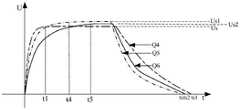
图12示出了不同触控显示器中像素单元在显示阶段内所接收到的数据信号的电压的一种曲线图;FIG. 12 shows a graph of the voltage of the data signal received by the pixel unit in the display stage in different touch displays;
图13示出了不同触控显示器中像素单元在显示阶段内所接收到的数据信号的电压的另一种曲线图;FIG. 13 shows another graph of the voltage of the data signal received by the pixel unit in the display stage in different touch displays;
图14为本发明实施例提供的一种触控显示驱动电路的结构示意图;FIG. 14 is a schematic structural diagram of a touch display driving circuit according to an embodiment of the present invention;
图15为本发明实施例提供的另一种触控显示驱动电路的结构示意图;FIG. 15 is a schematic structural diagram of another touch display driving circuit according to an embodiment of the present invention;
图16为本发明实施例提供的又一种触控显示驱动电路的结构示意图;FIG. 16 is a schematic structural diagram of another touch display driving circuit according to an embodiment of the present invention;
图17为本发明实施例提供的一种补偿模块的结构示意图。FIG. 17 is a schematic structural diagram of a compensation module according to an embodiment of the present invention.
此处的附图被并入说明书中并构成本说明书的一部分,示出了符合本申请的实施例,并与说明书一起用于解释本申请的原理。The accompanying drawings, which are incorporated in and constitute a part of this specification, illustrate embodiments consistent with the application and together with the description serve to explain the principles of the application.
具体实施方式Detailed ways
为了使本发明的目的、技术方案和优点更加清楚,下面将结合附图对本发明作进一步地详细描述,显然,所描述的实施例仅仅是本发明一部份实施例,而不是全部的实施例。基于本发明中的实施例,本领域普通技术人员在没有做出创造性劳动前提下所获得的所有其它实施例,都属于本发明保护的范围。In order to make the objectives, technical solutions and advantages of the present invention clearer, the present invention will be further described in detail below with reference to the accompanying drawings. Obviously, the described embodiments are only a part of the embodiments of the present invention, rather than all the embodiments. . Based on the embodiments of the present invention, all other embodiments obtained by those of ordinary skill in the art without creative efforts shall fall within the protection scope of the present invention.
在触控显示器显示一帧图像的过程中,在进入触控阶段时,该触控显示器中处于工作状态的GOA单元中存在残留电压,该残留电压会对该GOA单元所连接的一行像素单元中驱动晶体管的源极上施加的触控检测信号造成干扰,使得该行像素单元中每个像素单元中的像素电极和公共电极形成的像素电容会漏电,导致该行像素单元的显示亮度降低,触控显示器上出现暗横纹。In the process of displaying a frame of image on the touch display, when entering the touch stage, there is a residual voltage in the GOA unit in the working state in the touch display, and the residual voltage will be in a row of pixel units connected to the GOA unit. The touch detection signal applied to the source of the driving transistor causes interference, so that the pixel capacitance formed by the pixel electrode and the common electrode in each pixel unit in the row of pixel units will leak, resulting in a decrease in the display brightness of the row of pixel units, and the touch Dark horizontal streaks appear on the monitor.
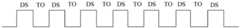
示例地,图1为相关技术提供的一种像素单元各个电极端的信号波形图,在显示阶段DS内,GOA单元向该像素单元中驱动晶体管的栅极G1施加栅极驱动信号,触控显示驱动电路向驱动晶体管的源极S1施加数据信号,并向该像素单元中的公共电极G2上施加公共电压Vcom。此时该像素单元的像素电极C上施加的电压较高。在进入触控阶段后TO后,GOA单元停止向该栅极施加栅极驱动信号,触控显示驱动电路向该公共电极G2和源极S1施加触控检测信号K1。此时,受GOA单元中残留电压的影响,如图1所示,施加在像素电极C上的电压会下降,导致该像素单元中像素电极和公共电极形成的像素电容漏电。1 is a signal waveform diagram of each electrode terminal of a pixel unit provided by the related art. In the display stage DS, the GOA unit applies a gate driving signal to the gate G1 of the driving transistor in the pixel unit, and the touch display The driving circuit applies the data signal to the source S1 of the driving transistor, and applies the common voltage Vcom to the common electrode G2 in the pixel unit. At this time, the voltage applied to the pixel electrode C of the pixel unit is relatively high. After entering the touch stage TO, the GOA unit stops applying the gate driving signal to the gate, and the touch display driving circuit applies the touch detection signal K1 to the common electrode G2 and the source S1. At this time, affected by the residual voltage in the GOA unit, as shown in FIG. 1 , the voltage applied to the pixel electrode C will drop, resulting in leakage of the pixel capacitor formed by the pixel electrode and the common electrode in the pixel unit.
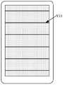
图2为相关技术提供的一种像素单元中栅极在触控显示器显示一帧显示图像内的波形图,触控显示器显示一帧图像的时间可以划分为7个显示阶段DS和6个触控阶段TO。此时,如图3所示,在该触控显示器显示的一帧图像中会存在6条暗横纹Y11。FIG. 2 is a waveform diagram of a gate in a pixel unit provided by the related art in displaying one frame of display image on the touch display. The time for the touch display to display one frame of image can be divided into seven display stages DS and six touch Stage TO. At this time, as shown in FIG. 3 , there are 6 dark horizontal stripes Y11 in one frame of image displayed by the touch display.
图4为本发明实施例提供的一种触控显示器的结构示意图,该触控显示驱动器可以包括:触控显示驱动电路11和多个GOA单元12,以及多个阵列排布的像素单元13,每个GOA单元12与一行像素单元连接,触控显示驱动电路11与每列像素单元连接。4 is a schematic structural diagram of a touch display according to an embodiment of the present invention. The touch display driver may include: a touch
其中,每个像素单元13可以包括:驱动晶体管T1、像素电容Clc以及存储电容Cst。该像素电容Clc也称为液晶电容,可以由像素电极和公共电极形成。该存储电容可以由像素电极和栅线形成。参考图4可以看出,每个GOA单元12的输出端OUT与一行像素单元中每个像素单元13的驱动晶体管T1的栅极连接。触控显示驱动电路11与每列像素单元中每个像素单元13中驱动晶体管T1的源极,以及公共电极连接。每个像素单元中的驱动晶体管T1的漏极与像素电极连接。Wherein, each
从图4中可以看出,每个GOA单元的输入端IN可以与位于该GOA单元前级的前级GOA单元的输出端OUT相连;每个GOA单元的复位端RST与位于该GOA单元后级的后级GOA单元的输出端OUT相连。As can be seen from FIG. 4 , the input terminal IN of each GOA unit can be connected to the output terminal OUT of the previous GOA unit located at the previous stage of the GOA unit; the reset terminal RST of each GOA unit is connected to the rear stage of the GOA unit. The output terminal OUT of the post-stage GOA unit is connected.
示例的,如图4所示,第n+m个GOA单元的输入端IN与第n个GOA单元的输出端OUT相连,且第n+m个GOA单元的复位端RST与第n+2m个GOA单元的输出端OUT相连。其中,n和m均为正整数,且均小于该触控显示器包括的GOA单元的总数。4, the input terminal IN of the n+mth GOA unit is connected to the output terminal OUT of the nth GOA unit, and the reset terminal RST of the n+mth GOA unit is connected to the n+2mth GOA unit. The output terminal OUT of the GOA unit is connected. Wherein, both n and m are positive integers, and both are smaller than the total number of GOA units included in the touch display.
图5为本发明实施例提供的一种像素单元的驱动方法流程图。该像素单元的驱动方法可以应用于图4所示的触控显示器的触控显示驱动电路。使用该像素单元的驱动方法驱动像素单元时可以避免触控显示器出现暗横纹。FIG. 5 is a flowchart of a method for driving a pixel unit according to an embodiment of the present invention. The driving method of the pixel unit can be applied to the touch display driving circuit of the touch display shown in FIG. 4 . When the pixel unit is driven by the driving method of the pixel unit, dark horizontal stripes on the touch display can be avoided.
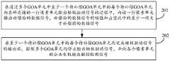
步骤201、在通过多个GOA单元中至少一个待补偿GOA单元中的每个待补偿GOA单元向其所连接的一行像素单元输出栅极驱动信号的过程中,向该一行像素单元输出补偿后的数据信号,补偿后的数据信号的幅值和占空比中的至少一项大于补偿前的数据信号。Step 201: In the process of outputting the gate drive signal to a row of pixel units to which it is connected through at least one GOA unit to be compensated in the multiple GOA units, output the compensated GOA unit to the row of pixel units. For the data signal, at least one of an amplitude value and a duty cycle of the data signal after compensation is greater than that of the data signal before compensation.
在该至少一个待补偿GOA单元中的每个GOA单元向其所连接的一行像素单元输出栅极驱动信号时,该行像素单元中的驱动晶体管开启,能够将数据信号写入与驱动晶体管连接的像素电极,此时该行像素单元发光,触控显示器处于显示阶段。When each GOA unit in the at least one GOA unit to be compensated outputs a gate driving signal to a row of pixel units to which it is connected, the driving transistors in the row of pixel units are turned on, and data signals can be written into the pixel units connected to the driving transistors. The pixel electrode, at this time, the row of pixel units emits light, and the touch display is in the display stage.
步骤202、在至少一个待补偿GOA单元中的每个待补偿GOA单元均完成栅极驱动信号的输出后,控制多个GOA单元均停止输出栅极驱动信号,并向各个像素单元的公共电极输出触控检测信号。Step 202: After each GOA unit to be compensated in the at least one GOA unit to be compensated completes the output of the gate drive signal, control the multiple GOA units to stop outputting the gate drive signal, and output the gate drive signal to the common electrode of each pixel unit. Touch detection signal.
在至少一个待补偿GOA单元中每个待补偿GOA单元完成栅极驱动信号的输出后,该触控显示器可以进入一个触控阶段。在该触控阶段内,触控显示驱动电路可以控制多个GOA单元均停止输出栅极驱动信号,并向各个像素单元的公共电极输出触控检测信号。此时,公共电极可以检测用户的触摸操作,并可以根据检测到的触摸操作向触控显示驱动电路反馈触控信号。After each GOA unit to be compensated in the at least one GOA unit to be compensated completes the output of the gate driving signal, the touch display can enter a touch phase. In this touch stage, the touch display driving circuit can control the plurality of GOA units to stop outputting gate driving signals, and output touch detection signals to the common electrodes of each pixel unit. At this time, the common electrode can detect a user's touch operation, and can feed back a touch signal to the touch display driving circuit according to the detected touch operation.
其中,每个待补偿GOA单元的复位端均与位于至少一个待补偿GOA单元后级的后级GOA单元的输出端连接。在多个GOA单元均停止输出栅极驱动信号时,由于至少一个待补偿GOA单元中,每个待补偿GOA单元的复位端均与位于至少一个待补偿GOA单元后级的后级GOA单元的输出端连接,因此,在进入触控阶段时,该至少一个待补偿GOA单元中每个待补偿GOA单元的复位端无法被复位。也即是,该至少一个待补偿GOA单元为在进入触控阶段时无法被复位的GOA单元。Wherein, the reset terminal of each GOA unit to be compensated is connected to the output terminal of the subsequent-stage GOA unit located at the subsequent stage of at least one GOA unit to be compensated. When multiple GOA units stop outputting gate drive signals, because in at least one GOA unit to be compensated, the reset terminal of each GOA unit to be compensated is connected to the output of the next-stage GOA unit located after the at least one GOA unit to be compensated Therefore, when entering the touch stage, the reset terminal of each GOA unit to be compensated in the at least one GOA unit to be compensated cannot be reset. That is, the at least one GOA unit to be compensated is a GOA unit that cannot be reset when entering the touch phase.
在使用本发明实施例提供的像素单元的驱动方法驱动像素单元的过程中,在显示阶段内,通过至少一个待补偿GOA单元中每个待补偿GOA单元向其所连接的一行像素单元输出栅极驱动信号的同时,向该一行像素单元输出补偿后的数据信号。由于该补偿后的数据信号的幅值和占空比中的至少一项大于补偿前的数据信号,且由于数据信号的电压与该数据信号的幅值正相关,数据信号的电压的持续时长与该数据信号的占空比正相关;因此在显示阶段内该一行像素单元中每个像素单元所接收到的数据信号的电压或数据信号的电压的持续时长中的至少一项大于未补偿的像素单元。从而在由显示阶段进入触控阶段时,该补偿后的像素单元所接收到数据信号的电压,可以补偿因该至少一个待补偿GOA单元中每个待补偿GOA单元无法复位而导致其所连接的一行像素单元中像素电容所漏的电量。由此可以避免在触控阶段内因该像素单元中像素电容漏电而导致该像素单元的亮度降低,从而可以避免触控显示器出现暗横纹,提高了触控显示器的显示效果。In the process of driving the pixel unit by using the driving method for the pixel unit provided by the embodiment of the present invention, in the display stage, each GOA unit to be compensated in the at least one GOA unit to be compensated is used to output a gate to a row of pixel units connected thereto. At the same time as the driving signal, the compensated data signal is output to the pixel unit of the row. Since at least one of the amplitude and duty cycle of the compensated data signal is greater than that of the data signal before compensation, and since the voltage of the data signal is positively correlated with the amplitude of the data signal, the duration of the voltage of the data signal is the same as that of the data signal. The duty cycle of the data signal is positively correlated; therefore at least one of the voltage of the data signal or the duration of the voltage of the data signal received by each pixel cell in the row of pixel cells is greater than the uncompensated pixel during the display phase unit. Therefore, when entering the touch stage from the display stage, the voltage of the data signal received by the compensated pixel unit can compensate for the fact that each GOA unit to be compensated in the at least one GOA unit to be compensated cannot be reset and the connected GOA unit cannot be reset. The amount of electricity leaked by pixel capacitors in a row of pixel units. In this way, it is possible to avoid the reduction of the brightness of the pixel unit due to the leakage of the pixel capacitor in the pixel unit during the touch phase, thereby avoiding dark horizontal stripes on the touch display, and improving the display effect of the touch display.
在本发明实施例中,触控显示器显示一帧图像的时间可以划分为多个显示阶段和多个触控阶段,每个触控阶段位于相邻两个显示阶段之间。相应的,触控显示器中的多个GOA单元可以划分为依次排序的多组GOA单元组,多组GOA单元组与多个显示阶段一一对应,且每组GOA单元组包括依次排列的多个GOA单元。触控显示驱动电路用于在每个显示阶段内,控制该显示阶段对应的一组GOA单元组对该组GOA单元组所连接的多行像素单元逐行输出栅极驱动信号。In the embodiment of the present invention, the time for the touch display to display one frame of image may be divided into multiple display stages and multiple touch stages, and each touch stage is located between two adjacent display stages. Correspondingly, the multiple GOA units in the touch display can be divided into multiple GOA unit groups arranged in sequence, the multiple GOA unit groups are in one-to-one correspondence with multiple display stages, and each GOA unit group includes sequentially arranged multiple GOA unit groups. GOA unit. The touch display driving circuit is used for controlling a group of GOA unit groups corresponding to the display phase to output gate driving signals row by row to the multiple rows of pixel units connected to the group of GOA unit groups in each display phase.
其中,该多组GOA单元组中除最后一组GOA单元组外的其他每组GOA单元组均可以包括至少一个待补偿GOA单元,该至少一个待补偿GOA单元为一组GOA单元组中排列在最后的若干个GOA单元。该排列在最后的若干个GOA单元中,每个GOA单元的复位端均与下一组GOA单元组中的GOA单元的输出端连接。该多组GOA单元组中的最后一组GOA单元组不包括待补偿GOA单元。Wherein, each GOA unit group except the last group of GOA unit groups in the multiple groups of GOA unit groups may include at least one GOA unit to be compensated, and the at least one GOA unit to be compensated is a group of GOA unit groups arranged in The last few GOA units. The arrangement is in the last several GOA units, and the reset terminal of each GOA unit is connected to the output terminal of the GOA unit in the next group of GOA unit groups. The last GOA unit group in the plurality of GOA unit groups does not include the GOA unit to be compensated.
请继续参考图4,触控显示器包括的多个GOA单元12中,每个GOA单元可以均与其相邻的GOA单元级联,即m可以等于1。此时,第n+1个GOA单元的输入端IN与第n个GOA单元的输出端OUT相连,第n+1个GOA单元的复位端RST与第n+2个GOA单元输出端OUT相连。在该级联场景下,多个GOA单元中的至少一个待补偿GOA单元可以仅包括一个待补偿GOA单元。Please continue to refer to FIG. 4 , among the plurality of
或者,触控显示器包括的多个GOA单元中,每个GOA单元可以均与其相隔若干GOA单元的GOA单元级联,即m可以大于1。Alternatively, in the multiple GOA units included in the touch display, each GOA unit may be cascaded with its GOA units separated by several GOA units, that is, m may be greater than 1.
示例地,如图6所示,例如,假设m=4,则第n+5个GOA单元的输入端IN与第n+1个GOA单元的输出端OUT相连,第n+1个GOA单元的复位端RST与和第n+5个GOA单元的输出端OUT相连。在该级联场景下,多个GOA单元中的至少一个待补偿GOA单元可以包括四个待补偿GOA单元。Illustratively, as shown in FIG. 6, for example, assuming that m=4, the input terminal IN of the n+5th GOA unit is connected to the output terminal OUT of the n+1th GOA unit, and the The reset terminal RST is connected to the output terminal OUT of the n+5th GOA unit. In this cascading scenario, at least one GOA unit to be compensated among the multiple GOA units may include four GOA units to be compensated.
可选地,从图4可以看出,阵列排布的多个像素单元13中任意两行像素单元13与触控显示驱动电路11的距离均不同。Optionally, as can be seen from FIG. 4 , the distances between any two rows of
图7为本发明实施例提供的另一种像素单元的驱动方法流程图。该像素单元的驱动方法可以应用于图4所示的触控显示器的触控显示驱动电路。FIG. 7 is a flowchart of another method for driving a pixel unit according to an embodiment of the present invention. The driving method of the pixel unit can be applied to the touch display driving circuit of the touch display shown in FIG. 4 .
步骤301、根据待补偿GOA单元所连接的一行像素单元与触控显示驱动电路之间的距离,对该一行像素单元的数据信号进行补偿,补偿后的数据信号的补偿值的高低与该距离的大小正相关。Step 301: Compensate the data signal of a row of pixel units according to the distance between a row of pixel units connected to the GOA unit to be compensated and the touch display driving circuit, and the compensation value of the compensated data signal is proportional to the distance. size is positively correlated.
其中,该补偿值为补偿后的数据信号对应的灰度值与补偿前的数据信号对应的灰度值的差值。The compensation value is the difference between the grayscale value corresponding to the data signal after compensation and the grayscale value corresponding to the data signal before compensation.
像素单元的数据信号对应的灰度值的大小可以与该数据信号的幅值大小正相关,即数据信号的幅值越大,其对应的灰度值就越大。像素单元的数据信号对应的灰度值的大小还可以与该数据信号的占空比大小正相关,即数据信号的占空比越大,其对应的灰度值就越大。The size of the gray value corresponding to the data signal of the pixel unit may be positively correlated with the amplitude of the data signal, that is, the larger the amplitude of the data signal, the larger the corresponding gray value. The size of the grayscale value corresponding to the data signal of the pixel unit may also be positively correlated with the duty cycle of the data signal, that is, the larger the duty cycle of the data signal, the greater the corresponding grayscale value.
本发明实施例中可以通过多种可实现方式根据一行像素单元与触控显示驱动电路之间的距离,对该一行像素单元的数据信号进行补偿,下面对该多种可实现方式中的两种可实现方式进行说明:In the embodiment of the present invention, the data signal of a row of pixel units can be compensated according to the distance between the pixel unit of a row and the touch display driving circuit in various achievable manners. The following two of the various achievable manners are as follows. A possible way to explain:
作为一种可选的实现方式,在多个GOA单元中,除最后一组GOA单元组外的其他每组GOA单元组仅包括一个待补偿GOA单元时,可以根据该其他每组GOA单元组中的待补偿GOA单元所连接的一行像素单元与触控显示驱动电路之间的距离,对该行像素单元的数据信号进行补偿,补偿后的数据信号的补偿值的高低与该距离的大小正相关。As an optional implementation manner, among multiple GOA units, when each other group of GOA unit groups except the last group of GOA unit groups only includes one GOA unit to be compensated, the The distance between a row of pixel units connected to the GOA unit to be compensated and the touch display driving circuit, the data signal of the row of pixel units is compensated, and the level of the compensation value of the compensated data signal is positively correlated with the size of the distance .
示例地,若该其他组GOA单元组中,一组GOA单元组中待补偿GOA单元所连接的第一行待补偿像素单元与触控显示驱动电路之间的距离为D1,另一组GOA组中待补偿GOA单元所连接的第二行待补偿像素单元与触控显示驱动电路之间的距离为D2,且D1<D2。则触控显示驱动电路对该第一行待补偿像素单元的数据信号进行补偿时的补偿值可以0.5,而对第二行待补偿像素单元的数据信号进行补偿时的补偿值可以为1.0。For example, if in the other group of GOA unit groups, the distance between the first row of pixel units to be compensated connected to the GOA unit to be compensated in one group of GOA unit groups and the touch display driving circuit is D1, and the distance between the other group of GOA unit groups is D1. The distance between the second row of pixel units to be compensated connected to the GOA unit to be compensated and the touch display driving circuit is D2, and D1<D2. Then, the compensation value when the touch display driving circuit compensates the data signals of the pixel units to be compensated in the first row may be 0.5, and the compensation value when compensating the data signals of the pixel units to be compensated in the second row may be 1.0.
作为另一种可选的实现方式,在多个GOA单元中,除最后一组GOA单元组外的其他每组GOA单元组包括多个待补偿GOA单元时,对于其他每组GOA单元组包括的多个待补偿GOA单元,可以根据每个待补偿GOA单元所连接的一行像素单元与触控显示驱动电路之间的距离,对该一行像素单元的数据信号进行补偿,补偿后的数据信号的补偿值的高低与该距离的大小正相关。As another optional implementation manner, in multiple GOA units, when each other GOA unit group except the last group of GOA unit groups includes multiple GOA units to be compensated, for each other group of GOA unit groups included A plurality of GOA units to be compensated can compensate the data signals of a row of pixel units according to the distance between a row of pixel units connected to each to-be-compensated GOA unit and the touch display driving circuit, and the compensation of the compensated data signals The value of the value is positively related to the size of the distance.
示例地,若其他每组GOA单元组包括4个待补偿GOA单元,则在沿远离触控显示驱动电路的方向上,触控显示驱动电路对该4个待补偿GOA单元所连接的4行像素单元的数据信号进行补偿时的补偿值可以依次为:0.5、1.0、1.5以及2.0。For example, if each other GOA unit group includes 4 GOA units to be compensated, then in the direction away from the touch display driver circuit, the touch display driver circuit connects the 4 rows of pixels to the 4 to be compensated GOA units. The compensation value when the data signal of the unit is compensated may be 0.5, 1.0, 1.5 and 2.0 in sequence.
可选地,在本发明实施例中,在对该其他组GOA单元组中,第一组GOA单元组中的第x个待补偿GOA单元所连接的一行像素单元的数据信号进行补偿时的补偿值,与对第二组GOA单元中的第x个待补偿GOA单元所连接的一行像素单元的数据信号进行补偿时的补偿值可以相同,也可以不同。其中,第一组GOA单元组和第二组GOA单元组中可以为其他组GOA单元组中的任意两组GOA单元组,第x个待补偿GOA单元可以为一组GOA单元组包括的多个待补偿GOA单元中的任意一个待补偿GOA单元。Optionally, in this embodiment of the present invention, in the other group of GOA unit groups, the compensation when the data signal of a row of pixel units connected to the xth GOA unit to be compensated in the first group of GOA unit groups is compensated. value, which may be the same as or different from the compensation value when compensating the data signal of a row of pixel units connected to the xth GOA unit to be compensated in the second group of GOA units. Wherein, the first group of GOA unit groups and the second group of GOA unit groups may be any two groups of GOA unit groups in other groups of GOA unit groups, and the xth GOA unit to be compensated may be a plurality of GOA unit groups included in one group of GOA unit groups Any one of the GOA units to be compensated is the GOA unit to be compensated.
可选地,在该其他组GOA单元组中,若第一组GOA单元组中第x个待补偿GOA单元所连接的一行像素单元与触控显示驱动电路的距离,小于第二组GOA单元组中第x个待补偿GOA单元所连接的一行像素单元与触控显示驱动电路的距离。则对该第一组GOA单元组中第x个待补偿GOA单元所连接的一行像素单元的数据信号进行补偿时的补偿值,可以小于对该第二组GOA单元组中第x个待补偿GOA单元所连接的一行像素单元的数据信号进行补偿时的补偿值。Optionally, in this other group of GOA unit groups, if the distance between a row of pixel units connected to the xth GOA unit to be compensated in the first group of GOA unit groups and the touch display driving circuit is smaller than that of the second group of GOA unit groups The distance between a row of pixel units connected to the xth GOA unit to be compensated and the touch display driving circuit. Then the compensation value when compensating the data signal of a row of pixel units connected to the xth GOA unit to be compensated in the first group of GOA units may be smaller than the xth GOA to be compensated in the second group of GOA units Compensation value when the data signal of a row of pixel units connected to the unit is compensated.
示例地,若除最后一组GOA单元组之外的其他每组GOA单元组中包括4个待补偿GOA单元。第一组GOA单元组中第1个待补偿GOA单元所连接的一行待补偿像素单元与触控显示驱动电路之间的距离为D3,第二组GOA单元组中第1个待补偿GOA单元所连接的一行待补偿像素单元与触控显示驱动电路之间的距离为D4,D3<D4。则触控显示驱动电路对第一组GOA单元组中第1个待补偿GOA单元所连接的一行像素单元的数据信号进行补偿时的补偿值可以为0.5,该触控显示驱动电路对第二组GOA单元组中第1个待补偿GOA单元所连接的一行像素单元的数据信号进行补偿时的补偿值可以为1.0。For example, if each group of GOA unit groups except the last group of GOA unit groups includes 4 GOA units to be compensated. The distance between a row of pixel units to be compensated connected to the first GOA unit to be compensated in the first group of GOA units and the touch display driving circuit is D3, and the distance between the first GOA unit to be compensated in the second group of GOA units is D3. The distance between the connected row of pixel units to be compensated and the touch display driving circuit is D4, D3<D4. Then, the compensation value when the touch display driving circuit compensates the data signal of the pixel unit of a row connected to the first GOA unit to be compensated in the first group of GOA unit groups may be 0.5, and the touch display driving circuit for the second group When the data signal of a row of pixel units connected to the first GOA unit to be compensated in the GOA unit group is compensated, the compensation value may be 1.0.
步骤302、在通过多个GOA单元中至少一个待补偿GOA单元中的每个待补偿GOA单元向其所连接的一行像素单元输出栅极驱动信号的过程中,向该一行像素单元输出补偿后的数据信号,补偿后的数据信号的幅值和占空比中的至少一项大于补偿前的数据信号。Step 302: In the process of outputting the gate drive signal to the row of pixel units to which it is connected through each GOA unit to be compensated in at least one GOA unit to be compensated in the plurality of GOA units, output the compensated pixel unit to the row of pixel units. For the data signal, at least one of an amplitude value and a duty cycle of the data signal after compensation is greater than that of the data signal before compensation.
触控显示驱动电路可以在除最后一个显示阶段外的其他每个显示阶段内,对该显示阶段对应的一组GOA单元中的至少一个待补偿GOA单元中,每个待补偿GOA单元所连接的一行像素单元输出补偿后的数据信号。且触控显示驱动电路可以在该显示阶段对应的一组GOA单元中的至少一个待补偿GOA单元均输出完栅极驱动信号后,插入一个触控阶段。The touch display drive circuit can in each display stage except the last display stage, in at least one GOA unit to be compensated in a group of GOA units corresponding to the display stage, the GOA unit to be compensated is connected to each GOA unit. One row of pixel units outputs the compensated data signal. And the touch display driving circuit can insert a touch stage after at least one of the GOA units to be compensated in the group of GOA units corresponding to the display stage has output the gate driving signal.
步骤303、在至少一个待补偿GOA单元中的每个待补偿GOA单元均完成栅极驱动信号的输出后,控制多个GOA单元均停止输出栅极驱动信号,并向各个像素单元的公共电极输出触控检测信号。Step 303: After each GOA unit to be compensated in the at least one GOA unit to be compensated completes the output of the gate drive signal, control the plurality of GOA units to stop outputting the gate drive signal, and output the gate drive signal to the common electrode of each pixel unit. Touch detection signal.
触控显示驱动电路在向各个像素单元的公共电极输出触控检测信号的过程中,还可以向各个像素单元中驱动晶体管的源极以及各个GOA单元中的时序信号控制端等信号端口也提供该触控检测信号,以保持该像素单元中像素电极和公共电极之间的像素电容的稳定性。In the process of outputting the touch detection signal to the common electrode of each pixel unit, the touch display driving circuit can also provide the signal port to the source of the driving transistor in each pixel unit and the timing signal control terminal in each GOA unit and other signal ports. The touch detection signal is used to maintain the stability of the pixel capacitance between the pixel electrode and the common electrode in the pixel unit.
在阵列排布的多个像素单元中任意两行像素单元与触控显示驱动电路的距离均不同的前提下,该多个像素单元中距离触控显示驱动电路越远的像素单元,与触控显示驱动电路之间的数据信号线越长,数据信号的电压损失的越多。On the premise that the distances between any two rows of pixel units and the touch display driving circuit are different in the plurality of pixel units arranged in the array, the pixel unit farther from the touch display driving circuit among the plurality of pixel units, is closer to the touch display driving circuit. The longer the data signal line between the display driving circuits, the more the voltage loss of the data signal.
而在上述步骤301中,通过对一行像素单元输出补偿值与该行像素单元与触控显示驱动电路的距离正相关的补偿后的数据信号,实现了对距离触控显示驱动电路较远的像素单元施加补偿值较大的数据信号,该补偿值较大的数据信号可以弥补这种损失。In the above-mentioned
需要说明的是,在上述步骤301中,触控显示驱动电路可以通过多种可实现方式对一行像素单元的数据信号进行补偿,下面对该多种可实现方式中的两种可实现方式进行说明:It should be noted that, in the
在第一种可实现方式中,可以先获取该一行像素单元中每个像素单元的灰度值,接着对该像素单元的灰度值进行补偿,之后可以对该像素单元的补偿后的灰度值进行数模转换,以得到该像素单元的补偿后的数据信号。In the first implementation manner, the grayscale value of each pixel unit in the row of pixel units can be obtained first, then the grayscale value of the pixel unit can be compensated, and then the compensated grayscale value of the pixel unit can be obtained. The value is digital-to-analog converted to obtain the compensated data signal of the pixel unit.
在第二种可实现方式中,在获取该一行像素单元中每个像素单元的灰度值后,对该像素单元的灰度值进行数模转换,以得到该像素单元的数据信号。之后对该像素单元的数据信号的幅值和占空比中的至少一项进行补偿,以得到该像素单元的补偿后的数据。In a second implementation manner, after acquiring the grayscale value of each pixel unit in the row of pixel units, digital-to-analog conversion is performed on the grayscale value of the pixel unit to obtain the data signal of the pixel unit. Then, at least one of the amplitude and duty cycle of the data signal of the pixel unit is compensated to obtain the compensated data of the pixel unit.
触控显示驱动电路在通过第一种可实现方式对待补偿GOA单元所连接的像素单元的数据信号进行补偿时,可以先获取该像素单元的显示数据(例如可以从内存中获取该像素单元的显示数据),该显示数据包括该像素单元的灰度值。接着触控显示驱动电路对该显示数据中的灰度值进行补偿(也即将该灰度值与补偿值相加),以形成补偿后的显示数据。之后触控显示驱动电路可以对该补偿后的显示数据进行数模转换,从而得到补偿后的数据信号。When compensating the data signal of the pixel unit connected to the GOA unit to be compensated by the first achievable method, the touch display driving circuit can first obtain the display data of the pixel unit (for example, the display data of the pixel unit can be obtained from the memory. data), the display data includes the gray value of the pixel unit. Then, the touch display driving circuit compensates the grayscale value in the display data (that is, adding the grayscale value and the compensation value) to form the compensated display data. Afterwards, the touch display driving circuit can perform digital-to-analog conversion on the compensated display data to obtain a compensated data signal.
需要说明的是,在触控显示驱动电路获取到待补偿GOA单元之外的GOA单元所连接的像素单元的显示数据后,可以对该像素单元的显示数据进行数模转换,从而得到数据信号。It should be noted that, after the touch display driving circuit obtains the display data of the pixel unit connected to the GOA unit other than the GOA unit to be compensated, it can perform digital-to-analog conversion on the display data of the pixel unit to obtain a data signal.
可选的,在触控显示驱动电路获取待补偿GOA单元所连接的像素单元的灰度值后,该触控显示驱动电路可以通过查询补偿表的方式,对该像素单元的灰度值进行补偿。该待补偿表中记录有每行像素单元在补偿前的数据信号对应的灰度值,以及在对待补偿GOA单元所连接的像素单元的灰度值进行补偿时的补偿值。Optionally, after the touch display driving circuit obtains the grayscale value of the pixel unit connected to the GOA unit to be compensated, the touch display driving circuit can compensate the grayscale value of the pixel unit by querying the compensation table. . The to-be-compensated table records the grayscale value corresponding to the data signal of each row of pixel units before compensation, and the compensation value when the grayscale value of the pixel unit connected to the to-be-compensated GOA unit is compensated.
示例地,假设触控显示器包括1920行像素单元,以及1920个GOA单元,该1920个GOA单元和1920行像素单元一一对应连接。该触控显示驱动电路设置在靠近第一行像素单元的位置处。该1920个GOA单元中的第n个GOA单元的复位端可以与第n+4(即m=4)个GOA单元的输出端连接。该1920个可以划分为依次排序的多组GOA单元组,该多组GOA单元中除最后一组GOA单元组外的其他每组GOA单元组均包括4个待补偿GOA单元。For example, it is assumed that the touch display includes 1920 rows of pixel units and 1920 GOA units, and the 1920 GOA units and 1920 rows of pixel units are connected in one-to-one correspondence. The touch display driving circuit is arranged at a position close to the first row of pixel units. The reset terminal of the nth GOA unit in the 1920 GOA units may be connected to the output terminal of the n+4th (ie, m=4)th GOA unit. The 1920 GOA unit groups can be divided into multiple groups of GOA unit groups in sequence, and each other group of GOA unit groups except the last group of GOA unit groups includes 4 GOA units to be compensated.
例如,第一组GOA单元组可以包括第1个GOA单元至第n1+4个GOA单元,其中,第n1+1个GOA单元至第n1+4个GOA单元为该第一组GOA单元组中的待补偿GOA单元。第二组GOA单元组可以包括第n1+5个GOA单元至第n2+4个GOA单元,其中,第n2+1个GOA单元至第n2+4个GOA单元为该第二组GOA单元组中的待补偿GOA单元。For example, the first GOA unit group may include the 1st GOA unit to the n1+4th GOA unit, wherein the n1+1th GOA unit to the n1+4th GOA unit are in the first group of GOA unit groups The GOA unit to be compensated. The second group of GOA unit groups may include the n1+5th GOA unit to the n2+4th GOA unit, wherein the n2+1th GOA unit to the n2+4th GOA unit are in the second group of GOA unit groups The GOA unit to be compensated.
触控显示驱动电路所存储的补偿表可以如表1所示,参考表1可以看出,在该1920行像素单元中,每个像素单元补偿前的灰度值可以均为Ga。第一组GOA单元组中的待补偿GOA单元所连接的像素单元为:第n1+1行像素单元至第n1+4行像素单元。在对该第n1+1行像素单元至第n1+4行像素单元的灰度值进行补偿时,由于第n1+1行像素单元与触控显示驱动电路之间的距离较近,第n1+4行像素单元与触控显示驱动电路之间的距离较远,因此,对于该n1+1行像素单元中每个像素单元的灰度值的补偿值可以为0.5;对于第n1+2行像素单元中每个像素单元的灰度值的补偿值可以为1.0;对于第n1+3行像素单元中每个像素单元的灰度值的补偿值可以为1.5;对于第n1+4行像素单元中每个像素单元的灰度值的补偿值可以为2.0。The compensation table stored in the touch display driving circuit can be shown in Table 1. Referring to Table 1, it can be seen that in the pixel unit of 1920 rows, the grayscale value of each pixel unit before compensation can be Ga. The pixel units connected to the GOA units to be compensated in the first group of GOA unit groups are: pixel units in the n1+1th row to pixel units in the n1+4th row. When compensating the grayscale values of the pixel units in the n1+1 row to the n1+4 row pixel units, because the distance between the n1+1 row pixel units and the touch display driving circuit is relatively short, the n1+ The distance between the 4 rows of pixel units and the touch display driving circuit is far, so the compensation value for the gray value of each pixel unit in the n1+1 row of pixel units can be 0.5; for the n1+2 row of pixels The compensation value of the gray value of each pixel unit in the unit may be 1.0; the compensation value of the gray value of each pixel unit in the pixel unit of the n1+3 row may be 1.5; for the pixel unit of the n1+4 row The compensation value of the gray value of each pixel unit may be 2.0.
第二组GOA单元组中的待补偿GOA单元所连接的像素单元为:第n2+1行像素单元至第n2+4行像素单元。在对该第n2+1行像素单元至第n2+4行像素单元的灰度值进行补偿时,由于第n2+1行像素单元与触控显示驱动电路之间的距离较近,第n2+4行像素单元与触控显示驱动电路之间的距离较远,因此,对于第n2+1行像素单元中每个像素单元的灰度值的补偿值可以为1.0;对于第n2+2行像素单元中每个像素单元的灰度值的补偿值可以为1.5;对于第n2+3行像素单元中每个像素单元的灰度值的补偿值可以为2.0;对于第n2+4行像素单元中每个像素单元的灰度值的补偿值可以为2.5。The pixel units connected to the GOA units to be compensated in the second group of GOA unit groups are: pixel units in the n2+1th row to pixel units in the n2+4th row. When compensating the grayscale values of the pixel units in the n2+1 row to the n2+4 row pixel units, due to the close distance between the n2+1 row pixel units and the touch display driving circuit, the n2+ The distance between the 4 rows of pixel units and the touch display driving circuit is relatively far, therefore, the compensation value for the gray value of each pixel unit in the n2+1 row of pixel units can be 1.0; for the n2+2 row of pixels The compensation value of the gray value of each pixel unit in the unit may be 1.5; the compensation value of the gray value of each pixel unit in the pixel unit of the n2+3 row may be 2.0; for the pixel unit of the n2+4 row The compensation value of the gray value of each pixel unit may be 2.5.
表1Table 1


可选地,触控显示驱动电路在获取待补偿的GOA单元所连接的像素单元的灰度值后可以锁存该灰度值,接着可以通过查询补偿表的方式对该灰度值进行补偿,并锁存补偿后的灰度值。之后可以对该补偿后的灰度值进行数模转换以得到补偿后的数据信号,接着可以放大该补偿后的数据信号。Optionally, the touch display driving circuit can latch the gray value after acquiring the gray value of the pixel unit connected to the GOA unit to be compensated, and then compensate the gray value by querying the compensation table, And latch the compensated gray value. Then, digital-to-analog conversion can be performed on the compensated grayscale value to obtain a compensated data signal, and then the compensated data signal can be amplified.
可选地,触控显示驱动电路在获取到待补偿GOA单元之外的GOA单元所连接的像素单元的灰度值后,可以锁存该灰度值,接着可以对该灰度值进行数模转换以得到数据信号。Optionally, after acquiring the grayscale value of the pixel unit connected to the GOA unit other than the GOA unit to be compensated, the touch display driving circuit can latch the grayscale value, and then perform a digital-analog on the grayscale value. converted to get the data signal.
在本发明实施例中,触控显示驱动电路生成的数据信号可以均为方波信号。In the embodiment of the present invention, the data signals generated by the touch display driving circuit may all be square wave signals.
在触控显示驱动电路通过第一种可实现方式对待补偿GOA单元所连接的像素单元的灰度值进行补偿,且在对该像素单元的补偿后的灰度值进行数模转换后,所得到的补偿后的数据信号的幅值可以大于补偿前的数据信号的幅值,或者,该补偿后的数据信号的占空比可以大于补偿前的数据信号的占空比,又或者,该补偿后的数据信号的幅值大于补偿前的数据信号的幅值,且占空比也大于补偿前的数据信号的占空比。After the touch display driving circuit compensates the grayscale value of the pixel unit connected to the GOA unit to be compensated in the first achievable manner, and performs digital-to-analog conversion on the compensated grayscale value of the pixel unit, the obtained The amplitude of the compensated data signal may be greater than the amplitude of the data signal before compensation, or the duty cycle of the compensated data signal may be greater than the duty cycle of the data signal before compensation, or, after the compensation The amplitude of the data signal is greater than the amplitude of the data signal before compensation, and the duty cycle is also greater than the duty cycle of the data signal before compensation.
触控显示驱动电路在通过第二种可实现方式对待补偿GOA单元所连接的像素单元的数据信号进行补偿时,在获取该像素单元的灰度值,并将该像素单元的灰度值进行数模转换以得到该像素单元的补偿前的数据信号后,可以通过提高该数据信号幅值和/或占空比的方式来对该数据信号的电压进行补偿,以获取该像素单元补偿后的数据信号。When compensating the data signal of the pixel unit connected to the GOA unit to be compensated by the second achievable method, the touch display driving circuit acquires the grayscale value of the pixel unit, and counts the grayscale value of the pixel unit. After analog conversion to obtain the data signal before the compensation of the pixel unit, the voltage of the data signal can be compensated by increasing the amplitude and/or duty cycle of the data signal to obtain the compensated data of the pixel unit Signal.
示例地,如图8所示,若某个像素单元的补偿前的数据信号F1的幅值为A1,且在该数据信号F1所在周期T1内,该数据信号F1的高电平的持续时长为T11。For example, as shown in FIG. 8 , if the amplitude of the data signal F1 before compensation of a certain pixel unit is A1, and in the period T1 where the data signal F1 is located, the duration of the high level of the data signal F1 is T11.
若触控显示驱动电路仅提高该数据信号的幅值,如图9所示,补偿后该数据信号F2的占空比(即每个周期内高电平的持续时长与周期的比值)可以保持不变。补偿后的数据信号F2的幅值由A1变为A2,且A2>A1。If the touch display driving circuit only increases the amplitude of the data signal, as shown in FIG. 9 , the duty cycle of the data signal F2 after compensation (ie the ratio of the duration of the high level to the cycle in each cycle) can be maintained constant. The amplitude of the compensated data signal F2 changes from A1 to A2, and A2>A1.
若触控显示驱动电路仅提高该数据信号的占空比,如图10所示,补偿后的数据信号F3的幅值A1保持不变,且该补偿后的数据信号F3的占空比由


若触控显示驱动电路同时提高该数据信号的幅值和占空比,如图11所示,补偿后的数据信号F4的幅值由A1变为A3,且A3>A1,且该补偿后的数据信号F4的占空比由


可选地,在至少一个待补偿GOA单元包括:多个待补偿GOA单元,对于该至少一个待补偿GOA单元所连接的至少一行像素单元,向任意两行相邻的像素单元所提供的补偿后的数据信号的补偿值的差值可以为目标差值。Optionally, at least one GOA unit to be compensated includes: a plurality of GOA units to be compensated, for at least one row of pixel units connected to the at least one GOA unit to be compensated, after compensation provided to any two rows of adjacent pixel units. The difference between the compensation values of the data signals may be the target difference.
这样一来,在该至少一行像素单元中,对任意两行相邻的像素单元所补偿的亮度值的差值均相同,使得不同行像素单元之间亮度过渡更自然。In this way, in the at least one row of pixel units, the difference in brightness values compensated for any two adjacent pixel units in any two rows is the same, so that the brightness transition between pixel units in different rows is more natural.
可选地,该目标差值可以小于或等于0.5。Optionally, the target difference may be less than or equal to 0.5.
由于人眼对两行相邻像素单元的数据信号的灰度值差小于或等于0.5时,该两行像素单元的亮度差的敏感度较小。因此,在对至少一行像素单元中,任意两行相邻的像素单元的补偿信号所施加的补偿值的差值可以小于或等于0.5时,该任意两行相邻的像素单元之间的亮度过渡更自然。Because the human eye is less sensitive to the difference in luminance between the two rows of adjacent pixel units when the grayscale value difference of the data signals of the two rows of adjacent pixel units is less than or equal to 0.5. Therefore, in at least one row of pixel units, when the difference between the compensation values applied by the compensation signals of any two rows of adjacent pixel units may be less than or equal to 0.5, the brightness transition between any two rows of adjacent pixel units more natural.
需要说明的是,在上述像素单元的驱动方法中,仅以触控显示驱动电路通过提高像素单元的数据信号的幅值的方式来对该数据信号进行补偿为例。可选地,触控显示驱动电路还可以仅通过提高像素单元的数据信号的占空比的方式来对该数据信号进行补偿。It should be noted that, in the above-mentioned driving method of the pixel unit, the touch display driving circuit only takes an example of compensating the data signal of the pixel unit by increasing the amplitude of the data signal. Optionally, the touch display driving circuit can also compensate the data signal only by increasing the duty ratio of the data signal of the pixel unit.
在触控显示驱动电路向像素单元输出数据信号的过程中,该数据信号在传输的过程中会发生损失,使得像素单元接收到的数据信号的波形与触控显示驱动电路所输出的数据信号的波形不同,且该波形呈曲线形。In the process of the touch display driving circuit outputting the data signal to the pixel unit, the data signal will be lost in the process of transmission, so that the waveform of the data signal received by the pixel unit and the data signal output by the touch display driving circuit The waveform is different, and the waveform is curved.
且不同触控显示器中像素单元在显示阶段内所接收到的数据信号的波形也不同,示例地,图12示出了不同触控显示器中像素单元在显示阶段内所接收到的数据信号的一种曲线图,且图12示出了在未对像素单元的数据信号进行补偿时该像素单元所接收到的数据信号的曲线图。纵坐标U表示像素单元接收到的数据信号的电压,横坐标t表示时间。图12示出了第一触控显示器中像素单元接收到的数据信号的曲线Q1,第二触控显示器中像素单元所接收到的数据信号的曲线Q2,以及第三触控显示器中像素单元所接收到的数据信号的曲线Q3。Moreover, the waveforms of the data signals received by the pixel units in different touch displays during the display phase are also different. For example, FIG. 12 shows a waveform of the data signals received by the pixel units in different touch displays during the display phase. 12 shows a graph of the data signal received by the pixel unit when the data signal of the pixel unit is not compensated. The ordinate U represents the voltage of the data signal received by the pixel unit, and the abscissa t represents the time. 12 shows the curve Q1 of the data signal received by the pixel unit in the first touch display, the curve Q2 of the data signal received by the pixel unit in the second touch display, and the curve Q2 of the data signal received by the pixel unit in the third touch display Curve Q3 of the received data signal.
假设每个触控显示器中触控显示驱动电路向像素单元输出的数据信号的波形相同,每个触控显示器中像素单元所接收到的数据信号的电压幅值均为Us,且每个显示器件中像素单元所接收到的数据信号的电压为高电压的阶段的持续时长均为ts。第一触控显示器中像素单元所接收到的数据信号的电压在时长t1内上升至电压幅值,第二触控显示器中像素单元所接收到的数据信号的电压在时长t2内上升至电压幅值,第三触控显示器中像素单元所接收到的数据信号的电压在时长t3内上升至电压幅值,且t1<t2<t3。Assuming that the waveform of the data signal output by the touch display drive circuit in each touch display to the pixel unit is the same, the voltage amplitude of the data signal received by the pixel unit in each touch display is Us, and each display device The duration of the phase in which the voltage of the data signal received by the middle pixel unit is a high voltage is all ts. The voltage of the data signal received by the pixel unit in the first touch display rises to the voltage amplitude within the duration t1, and the voltage of the data signal received by the pixel unit in the second touch display rises to the voltage amplitude within the duration t2 value, the voltage of the data signal received by the pixel unit in the third touch display rises to the voltage amplitude within the duration t3, and t1<t2<t3.
也即第一触控显示器中像素单元接收到数据信号的电压上升速度,大于第二触控显示器中像素单元接收到的数据信号的电压上升速度。第二触控显示器中像素单元接收到的数据信号的电压上升速度,大于第三触控显示器中像素单元接收到的数据信号的电压上升速度。对于同一个触控显示器触控显示驱动电路和像素单元,该触控显示驱动电路输出的数据信号的电压幅值,与该像素单元所接收的数据信号的电压上升速度正相关。That is, the voltage rising speed of the data signal received by the pixel unit in the first touch display is greater than the voltage rising speed of the data signal received by the pixel unit in the second touch display. The voltage rising speed of the data signal received by the pixel unit in the second touch display is greater than the voltage rising speed of the data signal received by the pixel unit in the third touch display. For the same touch display touch display drive circuit and pixel unit, the voltage amplitude of the data signal output by the touch display drive circuit is positively correlated with the voltage rise speed of the data signal received by the pixel unit.
图13示出了不同触控显示器中像素单元在显示阶段内所接收到的数据信号的另一种曲线图,且图13示出了在对像素单元的数据信号进行补偿时该像素单元所接收到的数据信号的曲线图。图13示出了第一触控显示器中像素单元接收到的数据信号的曲线Q4,第二触控显示器中像素单元接收到的数据信号的曲线Q5,以及第三触控显示器中像素单元接收到的数据信号的曲线Q6。FIG. 13 shows another graph of the data signals received by the pixel unit in the display stage in different touch displays, and FIG. 13 shows the data signal received by the pixel unit when the data signal of the pixel unit is compensated. Graph of the received data signal. FIG. 13 shows the curve Q4 of the data signal received by the pixel unit in the first touch display, the curve Q5 of the data signal received by the pixel unit in the second touch display, and the curve Q5 of the data signal received by the pixel unit in the third touch display curve Q6 of the data signal.
在对该第一触控显示器中像素单元的数据信号进行补偿时,第一触控显示器中触控显示驱动电路可以提高数据信号的占空比,以使该像素单元接收到的数据信号的电压的持续时长增至ts1。When compensating the data signal of the pixel unit in the first touch display, the touch display driving circuit in the first touch display can increase the duty cycle of the data signal, so that the voltage of the data signal received by the pixel unit is The duration increased to ts1.
在对第二触控显示其中像素单元的数据信号进行补偿时,第二触控显示器中触控显示驱动电路可以提高数据信号的幅值,以使该像素单元所接收到的数据信号的电压幅值增至Us1。且该像素单元所接收到的数据信号的电压在时长t4内上升至电压幅值,且t4<t2,也即提高了该像素单元的电压上升速度。When compensating the data signal of the pixel unit in the second touch display, the touch display driving circuit in the second touch display can increase the amplitude of the data signal, so that the voltage amplitude of the data signal received by the pixel unit The value is increased to Us1. In addition, the voltage of the data signal received by the pixel unit rises to the voltage amplitude within the duration t4, and t4<t2, that is, the voltage rising speed of the pixel unit is increased.
在对该第三触控显示器中像素单元的数据信号进行补偿时,第三触控显示器中触控显示驱动电路可以同时提高数据信号的幅值和占空比,以使该像素单元所接收到的数据信号的电压幅值增至Us2,该像素单元所接收到的数据信号的电压的持续时长增至ts2。且该像素单元所接收到的数据信号的电压在时长t5内上升至电压幅值,且t5<t3,也即提高了该像素单元的电压上升速度。When compensating the data signal of the pixel unit in the third touch display, the touch display driving circuit in the third touch display can simultaneously increase the amplitude and duty cycle of the data signal, so that the pixel unit receives The voltage amplitude of the data signal of the pixel unit increases to Us2, and the duration of the voltage of the data signal received by the pixel unit increases to ts2. In addition, the voltage of the data signal received by the pixel unit rises to the voltage amplitude within the duration t5, and t5<t3, that is, the voltage rising speed of the pixel unit is increased.
在多个GOA单元均停止输出栅极驱动信号时,由于至少一个待补偿GOA单元中,每个待补偿GOA单元的复位端均与位于至少一个待补偿GOA单元后级的后级GOA单元的输出端连接,因此,在进入触控阶段时,该至少一个待补偿GOA单元中每个待补偿GOA单元的复位端无法被复位。When multiple GOA units stop outputting gate drive signals, because in at least one GOA unit to be compensated, the reset terminal of each GOA unit to be compensated is connected to the output of the next-stage GOA unit located after the at least one GOA unit to be compensated Therefore, when entering the touch stage, the reset terminal of each GOA unit to be compensated in the at least one GOA unit to be compensated cannot be reset.
而在使用本发明实施例提供的像素单元的驱动方法驱动像素单元的过程中,在显示阶段内,通过至少一个待补偿GOA单元中每个待补偿GOA单元向其所连接的一行像素单元输出栅极驱动信号的同时,向该一行像素单元输出补偿后的数据信号。由于该补偿后的数据信号的幅值和占空比中的至少一项大于补偿前的数据信号,且由于数据信号的电压与该数据信号的幅值正相关,数据信号的电压的持续时长与该数据信号的占空比正相关;因此在显示阶段内该一行像素单元中每个像素单元所接收到的数据信号的电压或数据信号的电压的持续时长中的至少一项大于未补偿的像素单元。从而在由显示阶段进入触控阶段时,该补偿后的像素单元所接收到数据信号的电压,可以补偿因该至少一个待补偿GOA单元中每个待补偿GOA单元无法复位而导致其所连接的一行像素单元中像素电容所漏的电量。由此可以避免在触控阶段内因该像素单元中像素电容漏电而导致该像素单元的亮度降低,从而可以避免触控显示器出现暗横纹,提高了触控显示器的显示效果。In the process of driving the pixel unit using the driving method for the pixel unit provided by the embodiment of the present invention, in the display stage, each GOA unit to be compensated in the at least one GOA unit to be compensated is used to output the grid output to a row of pixel units connected to it. At the same time as the pole driving signal, the compensated data signal is output to the pixel unit of the row. Since at least one of the amplitude and duty cycle of the compensated data signal is greater than that of the data signal before compensation, and since the voltage of the data signal is positively correlated with the amplitude of the data signal, the duration of the voltage of the data signal is the same as that of the data signal. The duty cycle of the data signal is positively correlated; therefore at least one of the voltage of the data signal or the duration of the voltage of the data signal received by each pixel cell in the row of pixel cells is greater than the uncompensated pixel during the display phase unit. Therefore, when entering the touch stage from the display stage, the voltage of the data signal received by the compensated pixel unit can compensate for the fact that each GOA unit to be compensated in the at least one GOA unit to be compensated cannot be reset and the connected GOA unit cannot be reset. The amount of electricity leaked by pixel capacitors in a row of pixel units. In this way, it is possible to avoid the reduction of the brightness of the pixel unit due to the leakage of the pixel capacitor in the pixel unit during the touch phase, thereby avoiding dark horizontal stripes on the touch display, and improving the display effect of the touch display.
需要说明的是,本发明实施例提供的方法实施例步骤的先后顺序能够进行适当调整,步骤也能够根据情况进行相应增减,任何熟悉本技术领域的技术人员在本发明揭露的技术范围内,可轻易想到变化的方法,都应涵盖在本发明的保护范围之内,因此不再赘述。It should be noted that the sequence of steps in the method embodiments provided by the embodiments of the present invention can be appropriately adjusted, and the steps can also be increased or decreased according to the situation. Variations of methods that can be easily imagined should all be included within the protection scope of the present invention, and thus will not be described again.
图14为本发明实施例提供的一种触控显示驱动电路的结构示意图。包括:第一锁存器131、查表器132、第二锁存器133、数模转换器134以及放大器135。FIG. 14 is a schematic structural diagram of a touch display driving circuit according to an embodiment of the present invention. It includes: a first latch 131 , a table lookup device 132 , a
其中,第一锁存器131可以用于获取并锁存待补偿GOA单元所连接的像素单元的灰度值,并将该灰度值发送至查表器132。查表器132中可以存储有补偿表,该查表器132可以用于通过查询补偿表的方式对该灰度值进行补偿,并将补偿后的灰度值发送至第二锁存器133。第二锁存器133可以用于锁存该补偿后的灰度值,并将该补偿后的灰度值发送至数模转换器134。数模转换器134可以用于对该补偿后的灰度值进行数模转换以得到补偿后的数据信号,并可以将该补偿后的数据信号发送至放大器135。放大器135可以用于放大该补偿后的数据信号,并将放大后的该补偿后的数据信号输出至该像素单元。The first latch 131 may be used to acquire and latch the grayscale value of the pixel unit connected to the GOA unit to be compensated, and send the grayscale value to the table look-up device 132 . A compensation table may be stored in the table look-up unit 132 , and the table look-up unit 132 may be used to compensate the gray value by querying the compensation table, and send the compensated gray value to the
可选地,第一锁存器131还可以用于获取并锁存待补偿GOA单元之外的GOA单元所连接的像素单元的灰度值,并将该灰度值直接发送至第二锁存器133。第二锁存器133可以用于锁存该灰度值,并将该补灰度值发送至数模转换器134。数模转换器134可以用于对该灰度值进行数模转换以得到数据信号,并将该数据信号发送至放大器135。放大器135可以用于放大该数据信号,并将放大后的该数据信号输出至该像素单元。Optionally, the first latch 131 can also be used to acquire and latch the grayscale value of the pixel unit connected to the GOA unit other than the GOA unit to be compensated, and directly send the grayscale value to the second latch.
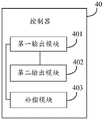
图15为本发明实施例提供的另一种触控显示驱动电路的结构示意图。该触控显示驱动电路应用于触控显示器,该触控显示器可以包括:触控显示驱动电路和级联的多个阵列基板行驱动GOA单元,以及多个阵列排布的像素单元,每个GOA单元与一行像素单元连接,触控显示驱动电路分别与每列像素单元连接。如图15所示,该触控显示驱动电路40可以包括:FIG. 15 is a schematic structural diagram of another touch display driving circuit according to an embodiment of the present invention. The touch display driving circuit is applied to a touch display, and the touch display may include: a touch display driving circuit, a plurality of array substrate row driving GOA units connected in cascade, and a plurality of pixel units arranged in an array, each GOA The unit is connected to a row of pixel units, and the touch display driving circuit is respectively connected to each column of pixel units. As shown in FIG. 15 , the touch
第一输出模块401,用于在通过多个GOA单元中至少一个待补偿GOA单元中的每个待补偿GOA单元向其所连接的一行像素单元输出栅极驱动信号的过程中,向一行像素单元输出补偿后的数据信号,补偿后的数据信号的幅值和占空比中的至少一项大于补偿前的数据信号。The
第二输出模块402,用于在至少一个待补偿GOA单元中的每个待补偿GOA均单元完成栅极驱动信号的输出后,控制多个GOA单元均停止输出栅极驱动信号,并向各个像素单元的公共电极输出触控检测信号。The
其中,每个待补偿GOA单元的复位端均与位于至少一个待补偿GOA单元后级的后级GOA单元的输出端连接。Wherein, the reset terminal of each GOA unit to be compensated is connected to the output terminal of the subsequent-stage GOA unit located at the subsequent stage of at least one GOA unit to be compensated.
在多个GOA单元均停止输出栅极驱动信号时,由于至少一个待补偿GOA单元中,每个待补偿GOA单元的复位端均与位于至少一个待补偿GOA单元后级的后级GOA单元的输出端连接,因此,在进入触控阶段时,该至少一个待补偿GOA单元中每个待补偿GOA单元的复位端无法被复位。When multiple GOA units stop outputting gate drive signals, because in at least one GOA unit to be compensated, the reset terminal of each GOA unit to be compensated is connected to the output of the next-stage GOA unit located after the at least one GOA unit to be compensated Therefore, when entering the touch stage, the reset terminal of each GOA unit to be compensated in the at least one GOA unit to be compensated cannot be reset.
本发明实施例提供了一种触控显示驱动电路,在显示阶段内,第一输出模块通过至少一个待补偿GOA单元中每个待补偿GOA单元向其所连接的一行像素单元输出栅极驱动信号的同时,向该一行像素单元输出补偿后的数据信号。由于该补偿后的数据信号的幅值和占空比中的至少一项大于补偿前的数据信号,且由于数据信号的电压与该数据信号的幅值正相关,数据信号的电压的持续时长与该数据信号的占空比正相关;因此在显示阶段内该一行像素单元中每个像素单元所接收到的数据信号的电压或数据信号的电压的持续时长中的至少一项大于未补偿的像素单元。从而由显示阶段进入触控阶段时,该补偿后的像素单元所接收到的数据信号的电压,可以补偿因该至少一个待补偿GOA单元中每个待补偿GOA单元无法复位而导致其所连接的一行像素单元中像素电容所漏的电量。由此可以避免在触控阶段内因该像素单元中像素电容漏电而导致该像素单元的亮度降低,从而可以避免触控显示器出现暗横纹,提高了触控显示器的显示效果。An embodiment of the present invention provides a touch display driving circuit. In a display stage, the first output module outputs a gate driving signal to a row of pixel units connected thereto through each GOA unit to be compensated in at least one GOA unit to be compensated At the same time, the compensated data signal is output to the row of pixel units. Since at least one of the amplitude and duty cycle of the compensated data signal is greater than that of the data signal before compensation, and since the voltage of the data signal is positively correlated with the amplitude of the data signal, the duration of the voltage of the data signal is the same as that of the data signal. The duty cycle of the data signal is positively correlated; therefore at least one of the voltage of the data signal or the duration of the voltage of the data signal received by each pixel cell in the row of pixel cells is greater than the uncompensated pixel during the display phase unit. Therefore, when the display stage enters the touch stage, the voltage of the data signal received by the compensated pixel unit can compensate for the fact that each GOA unit to be compensated in the at least one GOA unit to be compensated cannot be reset. The amount of electricity leaked by pixel capacitors in a row of pixel units. In this way, it is possible to avoid the reduction of the brightness of the pixel unit due to the leakage of the pixel capacitor in the pixel unit during the touch phase, thereby avoiding dark horizontal stripes on the touch display, and improving the display effect of the touch display.
可选地,任意两行像素单元与触控显示驱动电路的距离均不同。Optionally, the distances between any two rows of pixel units and the touch display driving circuit are different.
图16为本发明实施例提供的又一种触控显示驱动电路的结构示意图,在图15的基础上,该触控显示驱动电路40还可以包括:FIG. 16 is a schematic structural diagram of another touch display driving circuit according to an embodiment of the present invention. On the basis of FIG. 15 , the touch
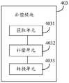
补偿模块403,用于根据待补偿GOA单元所连接的一行像素单元与触控显示驱动电路之间的距离,对一行素单元的数据信号进行补偿,补偿后的数据信号的补偿值的高低与距离的大小正相关,该补偿值为补偿后的数据信号对应的灰度值与补偿前的数据信号对应的灰度值的差值。The
可选地,如图17所示,该补偿模块403可以包括:Optionally, as shown in FIG. 17 , the
获取单元4031,用于获取待补偿GOA单元所连接的一行像素单元中每个像素单元的灰度值。The acquiring
补偿单元4032,用于对每个像素单元的灰度值进行补偿。The
转换单元4033,用于对每个像素单元的补偿后的灰度值进行数模转换,得到每个像素单元的补偿后的数据信号。The
可选地,触控显示驱动电路为触控显示芯片。Optionally, the touch display driving circuit is a touch display chip.
需要说明的是,触控显示芯片为同时具备触控驱动功能和显示驱动功能的芯片。It should be noted that the touch display chip is a chip having both a touch driving function and a display driving function.
可选的,该触控显示驱动电路还可以包括触控芯片和显示芯片,其中触控芯片具备触控驱动功能,显示芯片具备显示驱动功能。Optionally, the touch display driving circuit may further include a touch control chip and a display chip, wherein the touch control chip has a touch driving function, and the display chip has a display driving function.
在多个GOA单元均停止输出栅极驱动信号时,由于至少一个待补偿GOA单元中,每个待补偿GOA单元的复位端均与位于至少一个待补偿GOA单元后级的后级GOA单元的输出端连接,因此,在进入触控阶段时,该至少一个待补偿GOA单元中每个待补偿GOA单元的复位端无法被复位。When multiple GOA units stop outputting gate drive signals, because in at least one GOA unit to be compensated, the reset terminal of each GOA unit to be compensated is connected to the output of the next-stage GOA unit located after the at least one GOA unit to be compensated Therefore, when entering the touch stage, the reset terminal of each GOA unit to be compensated in the at least one GOA unit to be compensated cannot be reset.
本发明实施例提供了一种触控显示驱动电路,在显示阶段内,第一输出模块通过至少一个待补偿GOA单元中每个待补偿GOA单元向其所连接的一行像素单元输出栅极驱动信号的同时,向该一行像素单元输出补偿后的数据信号。由于该补偿后的数据信号的幅值和占空比中的至少一项大于补偿前的数据信号,且由于数据信号的电压与该数据信号的幅值正相关,数据信号的电压的持续时长与该数据信号的占空比正相关;因此在显示阶段内该一行像素单元中每个像素单元所接收到的数据信号的电压或数据信号的电压的持续时长中的至少一项大于未补偿的像素单元。从而由显示阶段进入触控阶段时,该补偿后的像素单元所接收到的数据信号的电压,可以补偿因该至少一个待补偿GOA单元中每个待补偿GOA单元无法复位而导致其所连接的一行像素单元中像素电容所漏的电量。由此可以避免在触控阶段内因该像素单元中像素电容漏电而导致该像素单元的亮度降低,从而可以避免触控显示器出现暗横纹,提高了触控显示器的显示效果。An embodiment of the present invention provides a touch display driving circuit. In a display stage, the first output module outputs a gate driving signal to a row of pixel units connected thereto through each GOA unit to be compensated in at least one GOA unit to be compensated At the same time, the compensated data signal is output to the row of pixel units. Since at least one of the amplitude and duty cycle of the compensated data signal is greater than that of the data signal before compensation, and since the voltage of the data signal is positively correlated with the amplitude of the data signal, the duration of the voltage of the data signal is the same as that of the data signal. The duty cycle of the data signal is positively correlated; therefore at least one of the voltage of the data signal or the duration of the voltage of the data signal received by each pixel cell in the row of pixel cells is greater than the uncompensated pixel during the display phase unit. Therefore, when the display stage enters the touch stage, the voltage of the data signal received by the compensated pixel unit can compensate for the fact that each GOA unit to be compensated in the at least one GOA unit to be compensated cannot be reset. The amount of electricity leaked by pixel capacitors in a row of pixel units. In this way, it is possible to avoid the reduction of the brightness of the pixel unit due to the leakage of the pixel capacitor in the pixel unit during the touch phase, thereby avoiding dark horizontal stripes on the touch display, and improving the display effect of the touch display.
需要说明的是,本发明实施例提供的触控显示驱动电路的实施例可以与像素单元的驱动方法实施例相互参考,本发明实施例对此不做限定。It should be noted that, the embodiments of the touch display driving circuit provided by the embodiments of the present invention may be referred to each other with the embodiments of the driving method of the pixel unit, which are not limited in the embodiments of the present invention.
本发明实施例还提供了一种触控显示器,该触控显示器包括上述触控显示驱动电路。An embodiment of the present invention further provides a touch display, the touch display including the above touch display driving circuit.
本领域技术人员在考虑说明书及实践这里公开的发明后,将容易想到本发明的其它实施方案。本申请旨在涵盖本发明的任何变型、用途或者适应性变化,这些变型、用途或者适应性变化遵循本发明的一般性原理并包括本发明未发明的本技术领域中的公知常识或惯用技术手段。说明书和实施例仅被视为示例性的,本发明的真正范围和精神由权利要求指出。Other embodiments of the invention will readily occur to those skilled in the art upon consideration of the specification and practice of the invention disclosed herein. This application is intended to cover any variations, uses or adaptations of the invention which follow the general principles of the invention and which include common knowledge or conventional techniques in the art to which the invention is not invented . The specification and examples are to be regarded as exemplary only, with the true scope and spirit of the invention being indicated by the claims.
应当理解的是,本发明并不局限于上面已经描述并在附图中示出的精确结构,并且可以在不脱离其范围进行各种修改和改变。本发明的范围仅由所附的权利要求来限制。It should be understood that the present invention is not limited to the precise structures described above and illustrated in the accompanying drawings, and that various modifications and changes may be made without departing from its scope. The scope of the present invention is limited only by the appended claims.
Claims (10)
Translated fromChinesePriority Applications (1)
| Application Number | Priority Date | Filing Date | Title |
|---|---|---|---|
| CN201910111058.6ACN109614014B (en) | 2019-02-12 | 2019-02-12 | Pixel unit driving method, touch display and touch display driving circuit |
Applications Claiming Priority (1)
| Application Number | Priority Date | Filing Date | Title |
|---|---|---|---|
| CN201910111058.6ACN109614014B (en) | 2019-02-12 | 2019-02-12 | Pixel unit driving method, touch display and touch display driving circuit |
Publications (2)
| Publication Number | Publication Date |
|---|---|
| CN109614014A CN109614014A (en) | 2019-04-12 |
| CN109614014Btrue CN109614014B (en) | 2022-04-19 |
Family
ID=66019716
Family Applications (1)
| Application Number | Title | Priority Date | Filing Date |
|---|---|---|---|
| CN201910111058.6AActiveCN109614014B (en) | 2019-02-12 | 2019-02-12 | Pixel unit driving method, touch display and touch display driving circuit |
Country Status (1)
| Country | Link |
|---|---|
| CN (1) | CN109614014B (en) |
Families Citing this family (5)
| Publication number | Priority date | Publication date | Assignee | Title |
|---|---|---|---|---|
| CN110277073A (en)* | 2019-06-12 | 2019-09-24 | 福建华佳彩有限公司 | A kind of double domain mode band ameliorative ways and storage equipment |
| CN110750170B (en)* | 2019-09-25 | 2023-08-29 | 昆山龙腾光电股份有限公司 | Embedded touch display panel, driving method thereof and display device |
| CN113407059A (en)* | 2021-06-25 | 2021-09-17 | 昆山龙腾光电股份有限公司 | Source data generation method, time sequence controller, display device and storage medium |
| CN113707067B (en)* | 2021-08-24 | 2023-09-01 | Tcl华星光电技术有限公司 | Display panel, driving method of display panel and electronic device |
| TWI822271B (en)* | 2022-08-25 | 2023-11-11 | 大陸商北京歐錸德微電子技術有限公司 | Display driving methods, driver chips and OLED touch displays to avoid interference with touch detection |
Citations (7)
| Publication number | Priority date | Publication date | Assignee | Title |
|---|---|---|---|---|
| CN103413524A (en)* | 2013-07-31 | 2013-11-27 | 京东方科技集团股份有限公司 | Organic light-emitting diode pixel circuit, method for driving same and display device |
| CN104078006A (en)* | 2014-06-27 | 2014-10-01 | 京东方科技集团股份有限公司 | Pixel circuit, display panel and display device |
| CN105609073A (en)* | 2016-01-07 | 2016-05-25 | 京东方科技集团股份有限公司 | Drive circuit, drive method, and display apparatus |
| CN106601173A (en)* | 2017-01-03 | 2017-04-26 | 京东方科技集团股份有限公司 | Sequential controller, pixel driving method and touch control display apparatus |
| CN107065253A (en)* | 2017-06-14 | 2017-08-18 | 厦门天马微电子有限公司 | Driving method, display panel and the display device of display panel |
| CN108269525A (en)* | 2017-01-03 | 2018-07-10 | 昆山国显光电有限公司 | AMOLED display device and its driving method |
| CN109144326A (en)* | 2018-05-31 | 2019-01-04 | 友达光电股份有限公司 | Touch display device and control method thereof |
Family Cites Families (1)
| Publication number | Priority date | Publication date | Assignee | Title |
|---|---|---|---|---|
| KR101448498B1 (en)* | 2012-06-13 | 2014-10-08 | 엘지디스플레이 주식회사 | Display device with integrated touch screen |
- 2019
- 2019-02-12CNCN201910111058.6Apatent/CN109614014B/enactiveActive
Patent Citations (7)
| Publication number | Priority date | Publication date | Assignee | Title |
|---|---|---|---|---|
| CN103413524A (en)* | 2013-07-31 | 2013-11-27 | 京东方科技集团股份有限公司 | Organic light-emitting diode pixel circuit, method for driving same and display device |
| CN104078006A (en)* | 2014-06-27 | 2014-10-01 | 京东方科技集团股份有限公司 | Pixel circuit, display panel and display device |
| CN105609073A (en)* | 2016-01-07 | 2016-05-25 | 京东方科技集团股份有限公司 | Drive circuit, drive method, and display apparatus |
| CN106601173A (en)* | 2017-01-03 | 2017-04-26 | 京东方科技集团股份有限公司 | Sequential controller, pixel driving method and touch control display apparatus |
| CN108269525A (en)* | 2017-01-03 | 2018-07-10 | 昆山国显光电有限公司 | AMOLED display device and its driving method |
| CN107065253A (en)* | 2017-06-14 | 2017-08-18 | 厦门天马微电子有限公司 | Driving method, display panel and the display device of display panel |
| CN109144326A (en)* | 2018-05-31 | 2019-01-04 | 友达光电股份有限公司 | Touch display device and control method thereof |
Non-Patent Citations (2)
| Title |
|---|
| Characterisation of inter-metal dielectric deposition processes on CMOS backplanes for liquid crystal on silicon microdisplays;Lee Y;《IEEE》;20041231;全文* |
| 硅基有机发光二极管微显示器的驱动技术研究;严利民;《中国博士学位论文全文数据库 信息科技辑》;20150730;全文* |
Also Published As
| Publication number | Publication date |
|---|---|
| CN109614014A (en) | 2019-04-12 |
Similar Documents
| Publication | Publication Date | Title |
|---|---|---|
| CN109614014B (en) | Pixel unit driving method, touch display and touch display driving circuit | |
| US5841410A (en) | Active matrix liquid crystal display and method of driving the same | |
| US10170068B2 (en) | Gate driving circuit, array substrate, display panel and driving method | |
| US4635127A (en) | Drive method for active matrix display device | |
| KR101493493B1 (en) | Backlight device and liquid crystal display device including the same | |
| CN109767737B (en) | Common voltage compensation method and display device thereof | |
| US11328650B2 (en) | Driver, display device and optical compensation method | |
| CN108319049B (en) | Liquid crystal display and driving method thereof | |
| US10957236B2 (en) | Driving method for source driver and related display system | |
| US20090085849A1 (en) | Fast Overdriving Method of LCD Panel | |
| US9711100B2 (en) | Common voltage distortion detecting circuit, liquid crystal display device and method of driving the same | |
| CN113811943B (en) | Display panel and display device | |
| JP4417839B2 (en) | Liquid crystal display | |
| KR102174474B1 (en) | Display and operation method therof | |
| CN119256350A (en) | Display device including LED driving circuit and operation method thereof | |
| CN111326126B (en) | Signal supply circuit, signal supply method and display device | |
| US6636196B2 (en) | Electro-optic display device using a multi-row addressing scheme | |
| KR101266066B1 (en) | Driving device, display apparatus having the same and method of driving the display apparatus | |
| US11451727B2 (en) | Pixel circuit, driving method thereof, array substrate and display device | |
| CN113658556B (en) | Voltage control circuit, control method and display device | |
| US12394390B2 (en) | Source driver having charge share line connecting output lines and display apparatus | |
| CN119380674B (en) | Driving module and display device | |
| CN117392961A (en) | Thrust control circuit and method of display driving circuit, display driver and device | |
| CN117321669A (en) | Driving method, driving circuit and display device of display panel | |
| US20080266274A1 (en) | Method of driving a display panel |
Legal Events
| Date | Code | Title | Description |
|---|---|---|---|
| PB01 | Publication | ||
| PB01 | Publication | ||
| SE01 | Entry into force of request for substantive examination | ||
| SE01 | Entry into force of request for substantive examination | ||
| GR01 | Patent grant | ||
| GR01 | Patent grant |