CN109584775B - Drive control circuit and display device - Google Patents
Drive control circuit and display deviceDownload PDFInfo
- Publication number
- CN109584775B CN109584775BCN201910005763.8ACN201910005763ACN109584775BCN 109584775 BCN109584775 BCN 109584775BCN 201910005763 ACN201910005763 ACN 201910005763ACN 109584775 BCN109584775 BCN 109584775B
- Authority
- CN
- China
- Prior art keywords
- transistor
- circuit
- control
- voltage
- terminal
- Prior art date
- Legal status (The legal status is an assumption and is not a legal conclusion. Google has not performed a legal analysis and makes no representation as to the accuracy of the status listed.)
- Active
Links
Images


Classifications
- G—PHYSICS
- G09—EDUCATION; CRYPTOGRAPHY; DISPLAY; ADVERTISING; SEALS
- G09G—ARRANGEMENTS OR CIRCUITS FOR CONTROL OF INDICATING DEVICES USING STATIC MEANS TO PRESENT VARIABLE INFORMATION
- G09G3/00—Control arrangements or circuits, of interest only in connection with visual indicators other than cathode-ray tubes
- G09G3/20—Control arrangements or circuits, of interest only in connection with visual indicators other than cathode-ray tubes for presentation of an assembly of a number of characters, e.g. a page, by composing the assembly by combination of individual elements arranged in a matrix no fixed position being assigned to or needed to be assigned to the individual characters or partial characters
- G09G3/22—Control arrangements or circuits, of interest only in connection with visual indicators other than cathode-ray tubes for presentation of an assembly of a number of characters, e.g. a page, by composing the assembly by combination of individual elements arranged in a matrix no fixed position being assigned to or needed to be assigned to the individual characters or partial characters using controlled light sources
- G09G3/30—Control arrangements or circuits, of interest only in connection with visual indicators other than cathode-ray tubes for presentation of an assembly of a number of characters, e.g. a page, by composing the assembly by combination of individual elements arranged in a matrix no fixed position being assigned to or needed to be assigned to the individual characters or partial characters using controlled light sources using electroluminescent panels
- G09G3/32—Control arrangements or circuits, of interest only in connection with visual indicators other than cathode-ray tubes for presentation of an assembly of a number of characters, e.g. a page, by composing the assembly by combination of individual elements arranged in a matrix no fixed position being assigned to or needed to be assigned to the individual characters or partial characters using controlled light sources using electroluminescent panels semiconductive, e.g. using light-emitting diodes [LED]
- G09G3/3208—Control arrangements or circuits, of interest only in connection with visual indicators other than cathode-ray tubes for presentation of an assembly of a number of characters, e.g. a page, by composing the assembly by combination of individual elements arranged in a matrix no fixed position being assigned to or needed to be assigned to the individual characters or partial characters using controlled light sources using electroluminescent panels semiconductive, e.g. using light-emitting diodes [LED] organic, e.g. using organic light-emitting diodes [OLED]
- G09G3/3225—Control arrangements or circuits, of interest only in connection with visual indicators other than cathode-ray tubes for presentation of an assembly of a number of characters, e.g. a page, by composing the assembly by combination of individual elements arranged in a matrix no fixed position being assigned to or needed to be assigned to the individual characters or partial characters using controlled light sources using electroluminescent panels semiconductive, e.g. using light-emitting diodes [LED] organic, e.g. using organic light-emitting diodes [OLED] using an active matrix
- G—PHYSICS
- G09—EDUCATION; CRYPTOGRAPHY; DISPLAY; ADVERTISING; SEALS
- G09G—ARRANGEMENTS OR CIRCUITS FOR CONTROL OF INDICATING DEVICES USING STATIC MEANS TO PRESENT VARIABLE INFORMATION
- G09G3/00—Control arrangements or circuits, of interest only in connection with visual indicators other than cathode-ray tubes
- G09G3/20—Control arrangements or circuits, of interest only in connection with visual indicators other than cathode-ray tubes for presentation of an assembly of a number of characters, e.g. a page, by composing the assembly by combination of individual elements arranged in a matrix no fixed position being assigned to or needed to be assigned to the individual characters or partial characters
- G09G3/34—Control arrangements or circuits, of interest only in connection with visual indicators other than cathode-ray tubes for presentation of an assembly of a number of characters, e.g. a page, by composing the assembly by combination of individual elements arranged in a matrix no fixed position being assigned to or needed to be assigned to the individual characters or partial characters by control of light from an independent source
- G09G3/36—Control arrangements or circuits, of interest only in connection with visual indicators other than cathode-ray tubes for presentation of an assembly of a number of characters, e.g. a page, by composing the assembly by combination of individual elements arranged in a matrix no fixed position being assigned to or needed to be assigned to the individual characters or partial characters by control of light from an independent source using liquid crystals
- G09G3/3611—Control of matrices with row and column drivers
- G09G3/3648—Control of matrices with row and column drivers using an active matrix
- G—PHYSICS
- G09—EDUCATION; CRYPTOGRAPHY; DISPLAY; ADVERTISING; SEALS
- G09G—ARRANGEMENTS OR CIRCUITS FOR CONTROL OF INDICATING DEVICES USING STATIC MEANS TO PRESENT VARIABLE INFORMATION
- G09G2310/00—Command of the display device
- G09G2310/02—Addressing, scanning or driving the display screen or processing steps related thereto
- G09G2310/0264—Details of driving circuits
- G09G2310/0294—Details of sampling or holding circuits arranged for use in a driver for data electrodes
- G—PHYSICS
- G09—EDUCATION; CRYPTOGRAPHY; DISPLAY; ADVERTISING; SEALS
- G09G—ARRANGEMENTS OR CIRCUITS FOR CONTROL OF INDICATING DEVICES USING STATIC MEANS TO PRESENT VARIABLE INFORMATION
- G09G2330/00—Aspects of power supply; Aspects of display protection and defect management
- G09G2330/02—Details of power systems and of start or stop of display operation
- G09G2330/025—Reduction of instantaneous peaks of current
- G—PHYSICS
- G09—EDUCATION; CRYPTOGRAPHY; DISPLAY; ADVERTISING; SEALS
- G09G—ARRANGEMENTS OR CIRCUITS FOR CONTROL OF INDICATING DEVICES USING STATIC MEANS TO PRESENT VARIABLE INFORMATION
- G09G2330/00—Aspects of power supply; Aspects of display protection and defect management
- G09G2330/02—Details of power systems and of start or stop of display operation
- G09G2330/026—Arrangements or methods related to booting a display
- G—PHYSICS
- G09—EDUCATION; CRYPTOGRAPHY; DISPLAY; ADVERTISING; SEALS
- G09G—ARRANGEMENTS OR CIRCUITS FOR CONTROL OF INDICATING DEVICES USING STATIC MEANS TO PRESENT VARIABLE INFORMATION
- G09G3/00—Control arrangements or circuits, of interest only in connection with visual indicators other than cathode-ray tubes
- G09G3/20—Control arrangements or circuits, of interest only in connection with visual indicators other than cathode-ray tubes for presentation of an assembly of a number of characters, e.g. a page, by composing the assembly by combination of individual elements arranged in a matrix no fixed position being assigned to or needed to be assigned to the individual characters or partial characters
- G09G3/22—Control arrangements or circuits, of interest only in connection with visual indicators other than cathode-ray tubes for presentation of an assembly of a number of characters, e.g. a page, by composing the assembly by combination of individual elements arranged in a matrix no fixed position being assigned to or needed to be assigned to the individual characters or partial characters using controlled light sources
- G09G3/30—Control arrangements or circuits, of interest only in connection with visual indicators other than cathode-ray tubes for presentation of an assembly of a number of characters, e.g. a page, by composing the assembly by combination of individual elements arranged in a matrix no fixed position being assigned to or needed to be assigned to the individual characters or partial characters using controlled light sources using electroluminescent panels
- G09G3/32—Control arrangements or circuits, of interest only in connection with visual indicators other than cathode-ray tubes for presentation of an assembly of a number of characters, e.g. a page, by composing the assembly by combination of individual elements arranged in a matrix no fixed position being assigned to or needed to be assigned to the individual characters or partial characters using controlled light sources using electroluminescent panels semiconductive, e.g. using light-emitting diodes [LED]
- G09G3/3208—Control arrangements or circuits, of interest only in connection with visual indicators other than cathode-ray tubes for presentation of an assembly of a number of characters, e.g. a page, by composing the assembly by combination of individual elements arranged in a matrix no fixed position being assigned to or needed to be assigned to the individual characters or partial characters using controlled light sources using electroluminescent panels semiconductive, e.g. using light-emitting diodes [LED] organic, e.g. using organic light-emitting diodes [OLED]
- G—PHYSICS
- G09—EDUCATION; CRYPTOGRAPHY; DISPLAY; ADVERTISING; SEALS
- G09G—ARRANGEMENTS OR CIRCUITS FOR CONTROL OF INDICATING DEVICES USING STATIC MEANS TO PRESENT VARIABLE INFORMATION
- G09G3/00—Control arrangements or circuits, of interest only in connection with visual indicators other than cathode-ray tubes
- G09G3/20—Control arrangements or circuits, of interest only in connection with visual indicators other than cathode-ray tubes for presentation of an assembly of a number of characters, e.g. a page, by composing the assembly by combination of individual elements arranged in a matrix no fixed position being assigned to or needed to be assigned to the individual characters or partial characters
- G09G3/34—Control arrangements or circuits, of interest only in connection with visual indicators other than cathode-ray tubes for presentation of an assembly of a number of characters, e.g. a page, by composing the assembly by combination of individual elements arranged in a matrix no fixed position being assigned to or needed to be assigned to the individual characters or partial characters by control of light from an independent source
- G09G3/36—Control arrangements or circuits, of interest only in connection with visual indicators other than cathode-ray tubes for presentation of an assembly of a number of characters, e.g. a page, by composing the assembly by combination of individual elements arranged in a matrix no fixed position being assigned to or needed to be assigned to the individual characters or partial characters by control of light from an independent source using liquid crystals
Landscapes
- Engineering & Computer Science (AREA)
- Physics & Mathematics (AREA)
- Computer Hardware Design (AREA)
- General Physics & Mathematics (AREA)
- Theoretical Computer Science (AREA)
- Chemical & Material Sciences (AREA)
- Crystallography & Structural Chemistry (AREA)
- Control Of Indicators Other Than Cathode Ray Tubes (AREA)
Abstract
Translated fromChinese
Description
Translated fromChinese技术领域technical field
本发明涉及电器技术领域,尤其涉及一种驱动控制电路及显示装置。The present invention relates to the technical field of electrical appliances, and in particular, to a drive control circuit and a display device.
背景技术Background technique
随着科技的进步,8K显示装置已成为各厂商研发的重点。With the advancement of technology, 8K display devices have become the focus of research and development by various manufacturers.
相关技术中,当8K显示装置主回路的电源电压上电启动时,由于负载较大且具有较强的感容性,上电瞬间电流较大,容易损害器件,降低器件使用寿命,并且容易对显示装置驱动集成电路(Integrated Circuit,简称IC)造成不可逆的损害。In the related art, when the power supply voltage of the main circuit of the 8K display device is powered on, due to the large load and strong inductance and capacitance, the instantaneous current at power-on is large, which is easy to damage the device, reduce the service life of the device, and is easy to damage the device. A display device driving integrated circuit (Integrated Circuit, IC for short) causes irreversible damage.
发明内容SUMMARY OF THE INVENTION
本发明旨在至少在一定程度上解决相关技术中的技术问题之一。The present invention aims to solve one of the technical problems in the related art at least to a certain extent.
为此,本发明的第一个目的在于提出一种驱动控制电路,在主回路的电源电压上电启动时,第一控制模块控制第一晶体管处于放大区不完全导通状态,以控制主回路电流,从而达到限流降压缓起的目的,保护器件及显示装置驱动IC,增加器件使用寿命。Therefore, the first object of the present invention is to provide a drive control circuit, when the power supply voltage of the main loop is powered on, the first control module controls the first transistor to be in an incomplete conduction state in the amplification region, so as to control the main loop current, so as to achieve the purpose of limiting the current and reducing the voltage, protecting the device and the driver IC of the display device, and increasing the service life of the device.
本发明的第二个目的在于提出一种显示装置。The second object of the present invention is to provide a display device.
为达上述目的,本发明第一方面实施例提出了一种驱动控制电路,包括:In order to achieve the above purpose, the embodiment of the first aspect of the present invention provides a drive control circuit, including:
第一晶体管,所述第一晶体管的第一端与主回路的电源电压连接,所述第一晶体管的第二端与第一接地端连接;a first transistor, the first end of the first transistor is connected to the power supply voltage of the main circuit, and the second end of the first transistor is connected to the first ground end;
第一控制模块,所述第一控制模块与所述第一晶体管的控制端连接,用于当所述主回路的电源电压上电启动时,控制所述第一晶体管处于放大区不完全导通状态。A first control module, the first control module is connected to the control terminal of the first transistor, and is used for controlling the first transistor to be in the amplifying region and not fully conducting when the power supply voltage of the main loop is powered on and started state.
根据本发明实施例提出的驱动控制电路,第一晶体管的第一端与主回路的电源电压连接,第一晶体管的第二端与第一接地端连接;第一控制模块与第一晶体管的控制端连接,当主回路的电源电压上电启动时,第一控制模块控制第一晶体管处于放大区不完全导通状态,以控制主回路电流,从而达到限流降压缓起的目的,保护器件及显示装置驱动IC,增加器件使用寿命。According to the drive control circuit proposed in the embodiment of the present invention, the first terminal of the first transistor is connected to the power supply voltage of the main circuit, the second terminal of the first transistor is connected to the first ground terminal; the first control module and the control of the first transistor When the power supply voltage of the main circuit is powered on, the first control module controls the first transistor to be in an incomplete conduction state in the amplifying area to control the current of the main circuit, so as to achieve the purpose of limiting the current and reducing the voltage, protecting the device and Display device driver IC to increase the service life of the device.
根据本发明的一个实施例,所述第一控制模块具体用于:当所述主回路的电源电压上电启动时,根据所述主回路中的电流调节输出至所述第一晶体管的控制端的第一驱动电压,以控制所述第一晶体管处于放大区不完全导通状态。According to an embodiment of the present invention, the first control module is specifically configured to: when the power supply voltage of the main loop is powered on, adjust the current output to the control end of the first transistor according to the current in the main loop a first driving voltage to control the first transistor to be in an incomplete conduction state of the amplifying region.
根据本发明的一个实施例,所述第一控制模块包括:采样电路,所述采样电路的第一端与所述第一晶体管的第二端连接,用于采集所述主回路中的电流,并根据所述主回路中的电流生成采样电压;差分放大电路,所述差分放大电路分别与所述采样电路的第一端和所述采样电路的第二端连接,用于对所述采样电压进行差分放大处理,得到第一电压;隔离采样电路,所述隔离采样电路与所述差分放大电路连接,用于对所述第一电压进行隔离处理,得到第二电压;积分放大电路,所述积分放大电路分别与所述隔离采样电路和所述第一晶体管的控制端连接,用于计算预设的第三电压与所述第二电压的差值,得到差值电压,并对所述差值电压进行积分放大处理,得到所述第一驱动电压输出至所述第一晶体管的控制端。According to an embodiment of the present invention, the first control module includes: a sampling circuit, a first end of the sampling circuit is connected to the second end of the first transistor, and is used for collecting the current in the main loop, and generate a sampling voltage according to the current in the main loop; a differential amplifying circuit, the differential amplifying circuit is connected to the first end of the sampling circuit and the second end of the sampling circuit respectively, and is used for the sampling voltage performing differential amplification processing to obtain a first voltage; isolating a sampling circuit, the isolation sampling circuit being connected to the differential amplifying circuit for performing isolation processing on the first voltage to obtain a second voltage; integrating amplifying circuit, the The integral amplifying circuit is respectively connected with the isolation sampling circuit and the control terminal of the first transistor, and is used for calculating the difference between the preset third voltage and the second voltage, obtaining the difference voltage, and comparing the difference The value voltage is integrated and amplified to obtain the first driving voltage and output to the control terminal of the first transistor.
根据本发明的一个实施例,所述第一控制模块还包括:第一二极管,所述积分放大电路通过所述第一二极管与所述第一晶体管的控制端连接,所述第一二极管的阳极与所述积分放大电路连接,所述第一二极管的阴极与所述第一晶体管的控制端连接。According to an embodiment of the present invention, the first control module further includes: a first diode, the integrating and amplifying circuit is connected to the control terminal of the first transistor through the first diode, and the first diode is connected to the control terminal of the first transistor. The anode of a diode is connected to the integrating amplifying circuit, and the cathode of the first diode is connected to the control terminal of the first transistor.
根据本发明的一个实施例,该驱动控制电路还包括:第二控制模块,所述第二控制模块与所述第一晶体管的控制端连接,用于当所述主回路的电源电压上电启动完成后,控制所述第一晶体管处于饱和区完全导通状态。According to an embodiment of the present invention, the drive control circuit further includes: a second control module, the second control module is connected to the control terminal of the first transistor, and is used for starting when the power supply voltage of the main circuit is powered on After completion, the first transistor is controlled to be in a fully conducting state in the saturation region.
根据本发明的一个实施例,所述第二控制模块具体用于:当所述主回路的电源电压上电启动完成后,根据输入的控制信号生成第二驱动电压输出至所述第一晶体管的控制端,所述第二驱动电压大于所述第一驱动电压,以控制所述第一晶体管处于饱和区完全导通状态。According to an embodiment of the present invention, the second control module is specifically configured to: after the power supply voltage of the main loop is completed, generate a second driving voltage according to the input control signal and output it to the first transistor. a control end, where the second driving voltage is greater than the first driving voltage, so as to control the first transistor to be in a fully conducting state in the saturation region.
根据本发明的一个实施例,所述第二控制模块包括:控制电路,用于根据所述控制信号生成第四电压;推挽电路,所述推挽电路分别与所述控制电路和所述第一晶体管的控制端连接,用于根据所述第四电压生成所述第二驱动电压。According to an embodiment of the present invention, the second control module includes: a control circuit for generating a fourth voltage according to the control signal; a push-pull circuit, the push-pull circuit is respectively connected with the control circuit and the first voltage A control end of a transistor is connected to generate the second driving voltage according to the fourth voltage.
根据本发明的一个实施例,所述控制电路包括:控制信号输入端,用于输入所述控制信号;光电耦合器,所述光电耦合器分别与所述控制信号输入端和所述推挽电路连接,用于在所述控制信号的控制下导通,生成所述第四电压。According to an embodiment of the present invention, the control circuit includes: a control signal input terminal for inputting the control signal; a photocoupler, which is respectively connected to the control signal input terminal and the push-pull circuit is connected to be turned on under the control of the control signal to generate the fourth voltage.
根据本发明的一个实施例,所述推挽电路包括:第二晶体管,所述第二晶体管的控制端与所述控制电路连接,用于在所述第四电压的控制下导通,所述第二晶体管的第一端用于输入第一隔离电压,所述第二晶体管的第二端与所述第一晶体管的控制端连接,所述第二晶体管的第二端用于输出所述第二驱动电压;第三晶体管,所述第三晶体管的第一端与所述第二晶体管的第二端连接,所述第三晶体管的第二端与所述第一接地端连接,所述第三晶体管的控制端与所述控制电路连接,用于在所述第四电压的控制下导通。According to an embodiment of the present invention, the push-pull circuit includes: a second transistor, a control end of the second transistor is connected to the control circuit, and is configured to be turned on under the control of the fourth voltage, the The first terminal of the second transistor is used to input the first isolation voltage, the second terminal of the second transistor is connected to the control terminal of the first transistor, and the second terminal of the second transistor is used to output the first isolation voltage. two driving voltages; a third transistor, the first terminal of the third transistor is connected to the second terminal of the second transistor, the second terminal of the third transistor is connected to the first ground terminal, the first terminal of the third transistor is connected to the second terminal of the second transistor The control terminals of the three transistors are connected to the control circuit for conducting under the control of the fourth voltage.
根据本发明的一个实施例,该驱动控制电路还包括:隔离电源电路,所述隔离电源电路分别与所述主回路的电源电压、所述第一控制模块和所述第二控制模块连接,用于根据所述主回路的电源电压生成所述第一控制模块和所述第二控制模块所需的工作电压或隔离工作电压。According to an embodiment of the present invention, the drive control circuit further includes: an isolated power supply circuit, the isolated power supply circuit is respectively connected to the power supply voltage of the main circuit, the first control module and the second control module, and uses The operating voltage or isolation operating voltage required by the first control module and the second control module is generated according to the power supply voltage of the main circuit.
为达上述目的,本发明第二方面实施例提出了一种显示装置,包括:如本发明第一方面实施例所述的驱动控制电路。In order to achieve the above object, an embodiment of the second aspect of the present invention provides a display device, including: the drive control circuit described in the embodiment of the first aspect of the present invention.
附图说明Description of drawings
图1是根据本发明一个实施例的驱动控制电路的结构图;1 is a structural diagram of a drive control circuit according to an embodiment of the present invention;
图2是根据本发明一个实施例的驱动控制电路的电路图;2 is a circuit diagram of a drive control circuit according to an embodiment of the present invention;
图3是根据本发明另一个实施例的驱动控制电路的结构图;3 is a structural diagram of a drive control circuit according to another embodiment of the present invention;
图4是根据本发明另一个实施例的驱动控制电路的电路图;4 is a circuit diagram of a drive control circuit according to another embodiment of the present invention;
图5是根据本发明一个实施例的显示装置的结构图。FIG. 5 is a structural diagram of a display device according to an embodiment of the present invention.
具体实施方式Detailed ways
下面详细描述本发明的实施例,所述实施例的示例在附图中示出,其中自始至终相同或类似的标号表示相同或类似的元件或具有相同或类似功能的元件。下面通过参考附图描述的实施例是示例性的,旨在用于解释本发明,而不能理解为对本发明的限制。The following describes in detail the embodiments of the present invention, examples of which are illustrated in the accompanying drawings, wherein the same or similar reference numerals refer to the same or similar elements or elements having the same or similar functions throughout. The embodiments described below with reference to the accompanying drawings are exemplary, and are intended to explain the present invention and should not be construed as limiting the present invention.
下面结合附图来描述本发明实施例的驱动控制电路及显示装置。The driving control circuit and the display device according to the embodiments of the present invention will be described below with reference to the accompanying drawings.
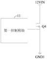
图1是根据本发明一个实施例的驱动控制电路的结构图,如图1所示,该驱动控制电路包括:FIG. 1 is a structural diagram of a drive control circuit according to an embodiment of the present invention. As shown in FIG. 1 , the drive control circuit includes:
第一晶体管Q4,第一晶体管Q4的第一端与主回路的电源电压12VIN连接,第一晶体管Q4的第二端与第一接地端GND1连接;The first transistor Q4, the first end of the first transistor Q4 is connected to the power supply voltage 12VIN of the main loop, and the second end of the first transistor Q4 is connected to the first ground terminal GND1;
第一控制模块11,第一控制模块11与第一晶体管Q4的控制端连接,用于当主回路的电源电压12VIN上电启动时,控制第一晶体管Q4处于放大区不完全导通状态。The
本发明实施例中,第一晶体管Q4具体可为如图1所示的金属-氧化物-半导体晶体管(Metal Oxide Semiconductor,简称MOS管),第一晶体管Q4的第一端具体可为MOS管的漏极,第一晶体管Q4的第二端具体可为MOS管的源极,第一晶体管Q4的控制端具体可为MOS管的栅极。第一晶体管Q4的第一端与主回路的电源电压12VIN连接,第一晶体管Q4的第二端与第一接地端GND1连接,第一控制模块11与第一晶体管Q4的控制端连接,当主回路的电源电压12VIN上电启动时,第一控制模块11控制第一晶体管Q4处于放大区不完全导通状态,以控制主回路电流,从而达到限流降压缓起的目的,保护器件及显示装置驱动IC,增加器件使用寿命。作为一种可行的实施方式,第一控制模块11可根据主回路中的电流I调节输出至第一晶体管Q4的控制端的第一驱动电压V4,以控制第一晶体管Q4处于放大区不完全导通状态。具体的,当I较小时,第一控制模块11可增大输出至第一晶体管Q4的控制端的第一驱动电压V4,控制第一晶体管Q4处于放大区不完全导通状态,增大I值,从而实现对主回流电流I的缓起控制;当I较大时,第一控制模块11可降低输出至第一晶体管Q4的控制端的第一驱动电压V4,控制第一晶体管Q4处于放大区不完全导通状态,降低I值,从而实现对主回流电流I的限流控制。In the embodiment of the present invention, the first transistor Q4 may specifically be a metal-oxide-semiconductor transistor (Metal Oxide Semiconductor, MOS transistor for short) as shown in FIG. 1 , and the first end of the first transistor Q4 may specifically be a MOS transistor. The drain, the second terminal of the first transistor Q4 may be the source of the MOS transistor, and the control terminal of the first transistor Q4 may be the gate of the MOS transistor. The first terminal of the first transistor Q4 is connected to the power supply voltage 12VIN of the main circuit, the second terminal of the first transistor Q4 is connected to the first ground terminal GND1, and the
根据本发明实施例提出的驱动控制电路,第一晶体管的第一端与主回路的电源电压连接,第一晶体管的第二端与第一接地端连接;第一控制模块与第一晶体管的控制端连接,当主回路的电源电压上电启动时,第一控制模块控制第一晶体管处于放大区不完全导通状态,以控制主回路电流,从而达到限流降压缓起的目的,保护器件及显示装置驱动IC,增加器件使用寿命。According to the drive control circuit proposed in the embodiment of the present invention, the first terminal of the first transistor is connected to the power supply voltage of the main circuit, the second terminal of the first transistor is connected to the first ground terminal; the first control module and the control of the first transistor When the power supply voltage of the main circuit is powered on, the first control module controls the first transistor to be in an incomplete conduction state in the amplifying area to control the current of the main circuit, so as to achieve the purpose of limiting the current and reducing the voltage, protecting the device and Display device driver IC to increase the service life of the device.
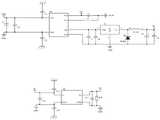
图2是根据本发明一个实施例的驱动控制电路的电路图,如图2所示,在图1所示实施例基础上,第一控制模块可包括:采样电路21、差分放大电路22、隔离采样电路23和积分放大电路24。2 is a circuit diagram of a drive control circuit according to an embodiment of the present invention. As shown in FIG. 2, based on the embodiment shown in FIG. 1, the first control module may include: a
采样电路21,采样电路21的第一端与第一晶体管Q4的第二端连接,用于采集主回路中的电流I,并根据主回路中的电流I生成采样电压△V。The
本发明实施例中,如图2所示,采样电路21具体可包括采样电阻R18和R19,当主回路的电源电压12VIN上电启动时,可通过R18和R19采集主回路的电流I,并根据采集的主回路的电流I生成采样电压△V=I*(R18*R19)/(R18+R19)。In the embodiment of the present invention, as shown in FIG. 2 , the
差分放大电路22,差分放大电路22分别与采样电路21的第一端和采样电路21的第二端连接,用于对采样电压△V进行差分放大处理,得到第一电压V1。The differential amplifying
本发明实施例中,如图2所示,差分放大电路22具体可包括:主回路的电源电压12VIN;接地端GND;电阻R15、R16、R17、R20和R21;电容C17;差分放大器U3A。差分放大电路22分别与采样电路21的第一端和采样电路21的第二端连接,具体的,可如图2所示,差分放大电路22中U3A的3脚通过R16与采样电路21中R18和R19的第一端连接,U3A的2脚通过R20与采样电路21中R18和R19的第二端连接,采样电路21获取采样电压△V后,将△V输出至差分放大电路22中的U3A,U3A对△V进行差分放大处理,得到第一电压V1,并在U3A的1脚输出。In the embodiment of the present invention, as shown in FIG. 2 , the
隔离采样电路23,隔离采样电路23与差分放大电路22连接,用于对第一电压V1进行隔离处理,得到第二电压V2。The
本发明实施例中,如图2所示,隔离采样电路23具体可包括:隔离芯片L2;接地端GND,接地端GND与L2的GND1引脚连接;第一接地端GND1,第一接地端GND1与L2的GND2引脚连接;电源电压5V(即5V的非隔离电压),电源电压5V与L2的输入引脚VDD1连接,用于为L2输入引脚VDD1提供5V电压,电源电压5V与主回路的电源电压12VIN共地,其电压参考地为GND;电源电压5V1(5V的隔离电压),电源电压5V1与L2的输出引脚VDD2连接,用于为L2输出引脚VDD2提供5V1电压,电源电压5V1的电压参考地为GND1;电容C18、C19和C20。隔离采样电路23与差分放大电路22连接,具体的,可如图2所示,隔离采样电路23中L2的VIN引脚通过R17与差分放大电路22中U3A的1脚连接,U3A的1脚输出第一电压V1至L2的VIN引脚,L2对V1进行隔离处理,得到第二电压V2,并在VO+引脚输出。In the embodiment of the present invention, as shown in FIG. 2, the
积分放大电路24,积分放大电路24分别与隔离采样电路22和第一晶体管Q4的控制端连接,用于计算预设的第三电压V3与第二电压V2的差值,得到差值电压V3-V2,并对差值电压V3-V2进行积分放大处理,得到第一驱动电压V4输出至第一晶体管Q4的控制端。The
本发明实施例中,如图2所示,积分放大电路24具体可包括:积分放大器U2A;电源电压5V1;电源电压12V1(即隔离的12V电压,其电压参考地为GND1);第一接地端GND1;电阻R6、R7、R8、R9、R10、R11和R13,其中,R6与R11起分压作用,用于对电源电压5V1进行分压,得到预设的第三电压V3,R7、R8、R10、R13用于确定U2A的放大倍数P;电容C10、C11和C13,其中,C10起积分作用,用于使电压放大不会出现倍数突变。积分放大电路24与隔离采样电路22相连,具体的,可如图2所示,隔离采样电路22中L2的VO+引脚通过R10与U2A的2脚相连,隔离采样电路22得到第二电压V2后,输出至U2A的2脚,电源电压5V1经R6及R11分压后,生成预设的第三电压V3并输出至U2A的3脚,U2A计算预设的第三电压V3与第二电压V2的差值,得到差值电压V3-V2,并对差值电压V3-V2进行积分放大处理,得到第一驱动电压V4=P*(V3-V2),输出至第一晶体管Q4的控制端。In the embodiment of the present invention, as shown in FIG. 2 , the integrating
本发明实施例的驱动控制电路的限流降压缓起控制原理如下:The current limiting step-down and slow-start control principle of the drive control circuit according to the embodiment of the present invention is as follows:
(1)当主回路的电源电压12VIN上电启动时,如果主回路的电流I偏大,则采样电路21生成采样电压△V偏大,差分放大电路22得到的第一电压V1偏大,隔离采样电路23得到的第二电压V2偏大,由于预设的第三电压V3为固定值,当V2偏大时,积分放大电路24得到第一驱动电压V4=P*(V3-V2)偏小,则输出至第一晶体管Q4的控制端的电压降低,Q4处于放大区不完全导通状态,降低主回路电流I值,使得Q4可实现对主回路电流I的限流控制。(1) When the power supply voltage 12VIN of the main circuit is powered on, if the current I of the main circuit is too large, the sampling voltage ΔV generated by the
(2)当主回路的电源电压12VIN上电启动时,如果主回路的电流I偏小,则采样电路21生成采样电压△V偏小,差分放大电路22得到的第一电压V1偏小,隔离采样电路23得到的第二电压V2偏小,由于预设的第三电压V3为固定值,当V2偏小时,积分放大电路24得到第一驱动电压V4=P*(V3-V2)偏大,则输出至第一晶体管Q4的控制端的电压增高,Q4处于放大区不完全导通状态,增大主回路电流I值,使得Q4可实现对主回路电流I的缓起控制。(2) When the power supply voltage 12VIN of the main loop is powered on, if the current I of the main loop is small, the sampling voltage ΔV generated by the
进一步的,如图2所示,第一控制模块还可包括:Further, as shown in FIG. 2, the first control module may further include:
第一二极管D2,积分放大电路24通过第一二极管D2与第一晶体管Q4的控制端连接,第一二极管D2的阳极与积分放大电路24连接,第一二极管D2的阴极与第一晶体管Q4的控制端连接。The first diode D2, the
进一步的,该驱动控制电路还可包括:Further, the drive control circuit may further include:
第二控制模块,第二控制模块与第一晶体管Q4的控制端连接,用于当主回路的电源电压12VIN上电启动完成后,控制第一晶体管Q4处于饱和区完全导通状态。The second control module, which is connected to the control terminal of the first transistor Q4, is used to control the first transistor Q4 to be in a fully conductive state in the saturation region after the power supply voltage 12VIN of the main loop is completed.
本发明实施例中,当主回路的电源电压12VIN上电启动完成后,第二控制模块控制第一晶体管Q4处于饱和区完全导通状态,以降低Q4功耗,使主回路以正常电流输出。具体的,第二控制模块可根据输入的控制信号生成第二驱动电压输出至第一晶体管Q4的控制端,第二驱动电压大于第一驱动电压V4,以控制第一晶体管Q4处于饱和区完全导通状态。In the embodiment of the present invention, after the power supply voltage 12VIN of the main loop is completed, the second control module controls the first transistor Q4 to be fully turned on in the saturation region, so as to reduce the power consumption of Q4 and enable the main loop to output a normal current. Specifically, the second control module can generate a second driving voltage and output it to the control terminal of the first transistor Q4 according to the input control signal. The second driving voltage is greater than the first driving voltage V4, so as to control the first transistor Q4 in the saturation region and completely conduct pass status.
进一步的,如图2所示,第二控制模块具体可包括:控制电路25和推挽电路26。Further, as shown in FIG. 2 , the second control module may specifically include: a
控制电路25,用于根据控制信号生成第四电压。The
本发明实施例中,控制电路25具体可包括:控制信号输入端IOI,用于输入控制信号;光电耦合器E1,光电耦合器E1分别与控制信号输入端IOI和推挽电路26连接,用于在控制信号的控制下导通,生成第四电压,其中,控制信号具体可为高电平信号。进一步的,如图2所示,控制电路25还可包括:电阻R1和R2;接地端GND;电源电压5V1。In the embodiment of the present invention, the
推挽电路26,推挽电路26分别与控制电路25和第一晶体管Q4的控制端连接,用于根据第四电压生成第二驱动电压。The push-
本发明实施例中,推挽电路26具体可包括:第二晶体管Q1,第二晶体管Q1的控制端与控制电路25连接,用于在第四电压的控制下导通,第二晶体管Q1的第一端用于输入第一隔离电压12V1,第二晶体管Q1的第二端与第一晶体管Q4的控制端连接,第二晶体管Q1的第二端用于输出第二驱动电压;第三晶体管Q3,第三晶体管Q3的第一端与第二晶体管Q1的第二端连接,第三晶体管Q3的第二端与第一接地端GND1连接,第三晶体管Q3的控制端与控制电路25连接,用于在第四电压的控制下导通。其中,第二晶体管Q1和第三晶体管Q3具体可为如图2所示的三极管,Q1的控制端具体可为三极管的基极,Q1的第一端具体可为三极管的集电极,Q1的第二端具体可为三极管的发射极,Q3的控制端具体可为三极管的基极,Q3的第一端具体可为三极管的发射极,Q3的第二端具体可为三极管的集电极。进一步的,如图2所示,推挽电路26还可包括电阻R4。In the embodiment of the present invention, the push-
本发明实施例的驱动控制电路的第二控制模块的工作原理如下:The working principle of the second control module of the drive control circuit according to the embodiment of the present invention is as follows:
当主回路的电源电压12VIN上电启动完成后,控制信号输入端IOI输入控制信号,光电耦合器E1接收到控制信号后,在控制信号的控制下导通,生成第四电压并将其输出至第二晶体管Q1和第三晶体管Q3的控制端,Q1、Q3在第四电压的控制下导通,第一隔离电压12V1与Q4之间的回路导通,第一隔离电压12V1输出至Q4的控制端(12V1与V4均与第一接地端GND1连接且12V1>V4,此时D2反向截止),控制第一晶体管Q4处于饱和区完全导通状态,降低Q4功耗,使主回路以正常电流输出。When the power supply voltage 12VIN of the main circuit is completed, the control signal input terminal IOI inputs the control signal, and after receiving the control signal, the optocoupler E1 is turned on under the control of the control signal to generate a fourth voltage and output it to the first The control terminals of the second transistor Q1 and the third transistor Q3, Q1 and Q3 are turned on under the control of the fourth voltage, the loop between the first isolation voltage 12V1 and Q4 is turned on, and the first isolation voltage 12V1 is output to the control terminal of Q4 (12V1 and V4 are both connected to the first ground terminal GND1 and 12V1>V4, at this time D2 is reversely turned off), control the first transistor Q4 to be in a fully conductive state in the saturation region, reduce the power consumption of Q4, and make the main loop output with normal current .
进一步的,该驱动控制电路还可包括稳压二极管D3和电阻R12。Further, the driving control circuit may further include a Zener diode D3 and a resistor R12.
根据本发明实施例提出的驱动控制电路,第一晶体管的第一端与主回路的电源电压连接,第一晶体管的第二端与第一接地端连接;第一控制模块与第一晶体管的控制端连接,当主回路的电源电压上电启动时,第一控制模块控制第一晶体管处于放大区不完全导通状态,以控制主回路电流,从而达到限流降压缓起的目的,保护器件及显示装置驱动IC,增加器件使用寿命。According to the drive control circuit proposed in the embodiment of the present invention, the first terminal of the first transistor is connected to the power supply voltage of the main circuit, the second terminal of the first transistor is connected to the first ground terminal; the first control module and the control of the first transistor When the power supply voltage of the main circuit is powered on, the first control module controls the first transistor to be in an incomplete conduction state in the amplifying area to control the current of the main circuit, so as to achieve the purpose of limiting the current and reducing the voltage, protecting the device and Display device driver IC to increase the service life of the device.
进一步的,如图3所示,图3是根据本发明另一个实施例的驱动控制电路的结构图,在图1所示实施例基础上,该驱动控制电路还可包括:Further, as shown in FIG. 3, FIG. 3 is a structural diagram of a drive control circuit according to another embodiment of the present invention. On the basis of the embodiment shown in FIG. 1, the drive control circuit may further include:
隔离电源电路13,隔离电源电路13分别与主回路的电源电压12VIN、第一控制模块11和第二控制模块12连接,用于根据主回路的电源电压12VIN生成第一控制模块11和第二控制模块12所需的工作电压或隔离工作电压。The isolated
本发明实施例中,隔离电源电路13可根据主回路的电源电压12VIN生成第一控制模块11和第二控制模块12所需的工作电压或隔离工作电压。In the embodiment of the present invention, the isolated
具体的,如图4所示,图4是根据本发明另一个实施例的驱动控制电路的电路图,隔离电源电路13可包括:主回路的电源电压12VIN;接地端GND;第一接地端GND1;电容C1、C2、C3、C4、C5、C6、C7、C8、C9、C12、C14、C15和C16;第一隔离电源模块M1;第二隔离电源模块M2;电感L1;二极管D1;电阻R14;电源电压5V;电源电压5V1;电源电压12V1。主回路的电源电压12VIN经第一隔离电源模块M1隔离后转换成电源电压12V1和电源电压5V,其中,电源电压12V1可为第一控制模块11提供隔离工作电压,具体可为第一控制模块11中的积分放大电路24提供12V的隔离工作电压,电源电压12V1还可为第二控制模块12提供隔离工作电压,具体可为第二控制模块12中的推挽电路26提供隔离工作电压;电源电压5V经第二隔离电源模块M2隔离后转换成电源电压5V1,电源电压5V1可为第一控制模块11提供隔离工作电压,具体可为第一控制模块11中的隔离采样电路23提供隔离工作电压;电源电压5V1还可为第二控制模块12提供隔离工作电压,具体可为第二控制模块12中的控制电路25提供隔离工作电压。Specifically, as shown in FIG. 4 , which is a circuit diagram of a drive control circuit according to another embodiment of the present invention, the isolated
根据本发明实施例提出的驱动控制电路,隔离电源电路可根据主回路的电源电压生成第一控制模块和第二控制模块所需的工作电压或隔离工作电压。According to the drive control circuit proposed in the embodiment of the present invention, the isolated power supply circuit can generate the working voltage or the isolated working voltage required by the first control module and the second control module according to the power supply voltage of the main loop.
为了实现上述实施例,本发明实施例还提出一种显示装置30,如图5所示,包括:如上述实施例所示的驱动控制电路31。所述显示装置可以为:液晶显示面板、电子纸、OLED面板、手机、平板电脑、电视机、显示器、笔记本电脑、数码相框、导航仪等任何具有显示功能的产品或部件。In order to realize the above-mentioned embodiment, an embodiment of the present invention further proposes a
在本说明书的描述中,参考术语“一个实施例”、“一些实施例”、“示例”、“具体示例”、或“一些示例”等的描述意指结合该实施例或示例描述的具体特征、结构、材料或者特点包含于本发明的至少一个实施例或示例中。在本说明书中,对上述术语的示意性表述不必针对的是相同的实施例或示例。而且,描述的具体特征、结构、材料或者特点可以在任一个或多个实施例或示例中以合适的方式结合。此外,在不相互矛盾的情况下,本领域的技术人员可以将本说明书中描述的不同实施例或示例以及不同实施例或示例的特征进行结合和组合。In the description of this specification, description with reference to the terms "one embodiment," "some embodiments," "example," "specific example," or "some examples", etc., mean specific features described in connection with the embodiment or example , structure, material or feature is included in at least one embodiment or example of the present invention. In this specification, schematic representations of the above terms are not necessarily directed to the same embodiment or example. Furthermore, the particular features, structures, materials or characteristics described may be combined in any suitable manner in any one or more embodiments or examples. Furthermore, those skilled in the art may combine and combine the different embodiments or examples described in this specification, as well as the features of the different embodiments or examples, without conflicting each other.
尽管上面已经示出和描述了本发明的实施例,可以理解的是,上述实施例是示例性的,不能理解为对本发明的限制,本领域的普通技术人员在本发明的范围内可以对上述实施例进行变化、修改、替换和变型。Although the embodiments of the present invention have been shown and described above, it should be understood that the above-mentioned embodiments are exemplary and should not be construed as limiting the present invention. Embodiments are subject to variations, modifications, substitutions and variations.
Claims (3)
Translated fromChinesePriority Applications (2)
| Application Number | Priority Date | Filing Date | Title |
|---|---|---|---|
| CN201910005763.8ACN109584775B (en) | 2019-01-03 | 2019-01-03 | Drive control circuit and display device |
| US16/665,049US11069287B2 (en) | 2019-01-03 | 2019-10-28 | Driver control circuit and display device |
Applications Claiming Priority (1)
| Application Number | Priority Date | Filing Date | Title |
|---|---|---|---|
| CN201910005763.8ACN109584775B (en) | 2019-01-03 | 2019-01-03 | Drive control circuit and display device |
Publications (2)
| Publication Number | Publication Date |
|---|---|
| CN109584775A CN109584775A (en) | 2019-04-05 |
| CN109584775Btrue CN109584775B (en) | 2022-04-08 |
Family
ID=65915548
Family Applications (1)
| Application Number | Title | Priority Date | Filing Date |
|---|---|---|---|
| CN201910005763.8AActiveCN109584775B (en) | 2019-01-03 | 2019-01-03 | Drive control circuit and display device |
Country Status (2)
| Country | Link |
|---|---|
| US (1) | US11069287B2 (en) |
| CN (1) | CN109584775B (en) |
Families Citing this family (4)
| Publication number | Priority date | Publication date | Assignee | Title |
|---|---|---|---|---|
| CN110071493A (en)* | 2019-04-25 | 2019-07-30 | 西安芯派电子科技有限公司 | A kind of adjustable circuit current-limiting method of current-limiting zone and current-limiting circuit |
| CN113508429B (en)* | 2019-09-17 | 2024-04-16 | 京东方科技集团股份有限公司 | Driving control circuit and driving method thereof and display panel |
| KR20230019352A (en)* | 2021-07-30 | 2023-02-08 | 삼성디스플레이 주식회사 | Display apparatus |
| CN114204516A (en)* | 2021-12-15 | 2022-03-18 | 惠州视维新技术有限公司 | A PMIC protection circuit and display device |
Citations (9)
| Publication number | Priority date | Publication date | Assignee | Title |
|---|---|---|---|---|
| CN1877675A (en)* | 2005-06-09 | 2006-12-13 | 东北先锋电子股份有限公司 | Drive apparatus and drive method for light emitting panel |
| DE102005039114A1 (en)* | 2005-08-18 | 2007-02-22 | Texas Instruments Deutschland Gmbh | Voltage regulator with a low voltage drop |
| TW201106786A (en)* | 2009-08-05 | 2011-02-16 | Advanced Connectek Inc | Constant current device and application thereof |
| JP2012049861A (en)* | 2010-08-27 | 2012-03-08 | Renesas Electronics Corp | Output circuit |
| CN105487588A (en)* | 2016-01-12 | 2016-04-13 | 四川长虹电器股份有限公司 | Constant current source circuit capable of being regulated and controlled in real time and constant current control method thereof |
| CN105934026A (en)* | 2016-05-11 | 2016-09-07 | 陕西亚成微电子股份有限公司 | Double-port constant current LED drive chip |
| CN106711948A (en)* | 2017-02-10 | 2017-05-24 | 中国第汽车股份有限公司 | Protective device and protective method for automotive direct current brush motor of current-free sensor |
| CN108449821A (en)* | 2018-02-23 | 2018-08-24 | 广东美的厨房电器制造有限公司 | Device and method for regulating the electromagnetic compatibility of a microwave device and microwave device |
| CN108806594A (en)* | 2018-06-08 | 2018-11-13 | 京东方科技集团股份有限公司 | Luminescence unit and its driving method, display device |
Family Cites Families (15)
| Publication number | Priority date | Publication date | Assignee | Title |
|---|---|---|---|---|
| DE69937560T2 (en)* | 1999-09-30 | 2008-09-04 | Asulab S.A. | Method and device for level shifting |
| JP4431364B2 (en)* | 2003-11-06 | 2010-03-10 | Okiセミコンダクタ株式会社 | Semiconductor chip for liquid crystal drive |
| US7312780B2 (en)* | 2004-02-27 | 2007-12-25 | Honeywell International, Inc. | Fluorescent lamp driver system |
| US7746170B2 (en)* | 2007-05-04 | 2010-06-29 | Micron Technology, Inc. | Class AB amplifier and imagers and systems using same |
| JP4508222B2 (en)* | 2007-08-31 | 2010-07-21 | ソニー株式会社 | Precharge control method and display device |
| CN202102692U (en)* | 2011-06-16 | 2012-01-04 | 青岛海信电器股份有限公司 | LED (light-emitting diode) drive circuit and LCD TV (liquid crystal television) |
| JP5891492B2 (en)* | 2011-06-22 | 2016-03-23 | 株式会社Joled | Display element, display device, and electronic device |
| US9582017B2 (en)* | 2013-07-02 | 2017-02-28 | Stmicroelectronics Design And Application S.R.O. | Method of preventing inversion of output current flow in a voltage regulator and related voltage regulator |
| KR102208396B1 (en)* | 2013-12-30 | 2021-01-26 | 엘지디스플레이 주식회사 | Power supplying apparatus and display apparatus including the same |
| CN105046247B (en)* | 2015-08-31 | 2018-06-22 | 京东方科技集团股份有限公司 | Surface texture recognition unit, circuit and recognition methods and electronic equipment |
| CN105118472A (en)* | 2015-10-08 | 2015-12-02 | 重庆京东方光电科技有限公司 | Gate drive device of pixel array and drive method for gate drive device |
| CN105469742B (en)* | 2016-01-15 | 2018-11-13 | 京东方科技集团股份有限公司 | A kind of organic light emitting display and display device |
| CN206077778U (en)* | 2016-10-09 | 2017-04-05 | 武汉通畅汽车电子照明有限公司 | LED blood pressure lowering drive circuits |
| CN107066019A (en)* | 2017-06-09 | 2017-08-18 | 电子科技大学 | A kind of current foldback circuit of negative pressure output type low pressure difference linear voltage regulator |
| CN107492333B (en)* | 2017-10-11 | 2020-07-17 | 京东方科技集团股份有限公司 | Defect detection method, device and display module of external compensation line |
- 2019
- 2019-01-03CNCN201910005763.8Apatent/CN109584775B/enactiveActive
- 2019-10-28USUS16/665,049patent/US11069287B2/enactiveActive
Patent Citations (9)
| Publication number | Priority date | Publication date | Assignee | Title |
|---|---|---|---|---|
| CN1877675A (en)* | 2005-06-09 | 2006-12-13 | 东北先锋电子股份有限公司 | Drive apparatus and drive method for light emitting panel |
| DE102005039114A1 (en)* | 2005-08-18 | 2007-02-22 | Texas Instruments Deutschland Gmbh | Voltage regulator with a low voltage drop |
| TW201106786A (en)* | 2009-08-05 | 2011-02-16 | Advanced Connectek Inc | Constant current device and application thereof |
| JP2012049861A (en)* | 2010-08-27 | 2012-03-08 | Renesas Electronics Corp | Output circuit |
| CN105487588A (en)* | 2016-01-12 | 2016-04-13 | 四川长虹电器股份有限公司 | Constant current source circuit capable of being regulated and controlled in real time and constant current control method thereof |
| CN105934026A (en)* | 2016-05-11 | 2016-09-07 | 陕西亚成微电子股份有限公司 | Double-port constant current LED drive chip |
| CN106711948A (en)* | 2017-02-10 | 2017-05-24 | 中国第汽车股份有限公司 | Protective device and protective method for automotive direct current brush motor of current-free sensor |
| CN108449821A (en)* | 2018-02-23 | 2018-08-24 | 广东美的厨房电器制造有限公司 | Device and method for regulating the electromagnetic compatibility of a microwave device and microwave device |
| CN108806594A (en)* | 2018-06-08 | 2018-11-13 | 京东方科技集团股份有限公司 | Luminescence unit and its driving method, display device |
Also Published As
| Publication number | Publication date |
|---|---|
| US20200219442A1 (en) | 2020-07-09 |
| CN109584775A (en) | 2019-04-05 |
| US11069287B2 (en) | 2021-07-20 |
Similar Documents
| Publication | Publication Date | Title |
|---|---|---|
| CN109584775B (en) | Drive control circuit and display device | |
| TWI339481B (en) | Power supplying and discharging circuit | |
| CN102117089A (en) | low dropout voltage regulator | |
| CN206619901U (en) | A kind of DC DC power modules and electronic equipment | |
| US7745960B2 (en) | Power supply control signal generating circuit | |
| CN105553256B (en) | Charge pump circuit and display device | |
| CN102081449A (en) | Video card power circuit | |
| CN103199488A (en) | Low-voltage protection circuit free of requiring independent reference source | |
| CN101471601B (en) | Charge pump for increased power efficiency and output voltage | |
| CN103474033B (en) | Boost control circuit and control method, booster circuit, display device | |
| CN111399617B (en) | Power supply control device and electronic apparatus | |
| CN113508429B (en) | Driving control circuit and driving method thereof and display panel | |
| CN112667019A (en) | Apply to soft start circuit of power saving province area of LDO | |
| CN117524162A (en) | Common mode voltage generation circuit and control method, chip, electronic equipment | |
| CN107547052B (en) | Embedded multiplier and operational amplifier | |
| CN114639360B (en) | Display panel and display device | |
| CN208298052U (en) | A kind of novel slew rate enhancing circuit, low pressure difference linear voltage regulator | |
| US20140292258A1 (en) | Electronic device and charging circuit thereof | |
| CN215186679U (en) | Control circuit of electronic equipment | |
| CN114764125A (en) | Testing device for low dropout regulator | |
| CN218997938U (en) | Power circuit and display module | |
| CN115149800B (en) | Power supply control circuit, power supply control method and display device | |
| CN223067085U (en) | Switch circuit, controller and electrical equipment | |
| CN114822359B (en) | Driving circuit, driving method and display device | |
| CN204794658U (en) | A base voltage control circuit for stepping up framework |
Legal Events
| Date | Code | Title | Description |
|---|---|---|---|
| PB01 | Publication | ||
| PB01 | Publication | ||
| SE01 | Entry into force of request for substantive examination | ||
| SE01 | Entry into force of request for substantive examination | ||
| GR01 | Patent grant | ||
| GR01 | Patent grant |