CN109523954B - Pixel unit, display panel, driving method and compensation control method - Google Patents
Pixel unit, display panel, driving method and compensation control methodDownload PDFInfo
- Publication number
- CN109523954B CN109523954BCN201811582314.1ACN201811582314ACN109523954BCN 109523954 BCN109523954 BCN 109523954BCN 201811582314 ACN201811582314 ACN 201811582314ACN 109523954 BCN109523954 BCN 109523954B
- Authority
- CN
- China
- Prior art keywords
- circuit
- driving circuit
- control
- data
- pixel
- Prior art date
- Legal status (The legal status is an assumption and is not a legal conclusion. Google has not performed a legal analysis and makes no representation as to the accuracy of the status listed.)
- Active
Links
Images


Classifications
- G—PHYSICS
- G09—EDUCATION; CRYPTOGRAPHY; DISPLAY; ADVERTISING; SEALS
- G09G—ARRANGEMENTS OR CIRCUITS FOR CONTROL OF INDICATING DEVICES USING STATIC MEANS TO PRESENT VARIABLE INFORMATION
- G09G3/00—Control arrangements or circuits, of interest only in connection with visual indicators other than cathode-ray tubes
- G09G3/20—Control arrangements or circuits, of interest only in connection with visual indicators other than cathode-ray tubes for presentation of an assembly of a number of characters, e.g. a page, by composing the assembly by combination of individual elements arranged in a matrix no fixed position being assigned to or needed to be assigned to the individual characters or partial characters
- G09G3/22—Control arrangements or circuits, of interest only in connection with visual indicators other than cathode-ray tubes for presentation of an assembly of a number of characters, e.g. a page, by composing the assembly by combination of individual elements arranged in a matrix no fixed position being assigned to or needed to be assigned to the individual characters or partial characters using controlled light sources
- G09G3/30—Control arrangements or circuits, of interest only in connection with visual indicators other than cathode-ray tubes for presentation of an assembly of a number of characters, e.g. a page, by composing the assembly by combination of individual elements arranged in a matrix no fixed position being assigned to or needed to be assigned to the individual characters or partial characters using controlled light sources using electroluminescent panels
- G09G3/32—Control arrangements or circuits, of interest only in connection with visual indicators other than cathode-ray tubes for presentation of an assembly of a number of characters, e.g. a page, by composing the assembly by combination of individual elements arranged in a matrix no fixed position being assigned to or needed to be assigned to the individual characters or partial characters using controlled light sources using electroluminescent panels semiconductive, e.g. using light-emitting diodes [LED]
- G09G3/3208—Control arrangements or circuits, of interest only in connection with visual indicators other than cathode-ray tubes for presentation of an assembly of a number of characters, e.g. a page, by composing the assembly by combination of individual elements arranged in a matrix no fixed position being assigned to or needed to be assigned to the individual characters or partial characters using controlled light sources using electroluminescent panels semiconductive, e.g. using light-emitting diodes [LED] organic, e.g. using organic light-emitting diodes [OLED]
- G09G3/3225—Control arrangements or circuits, of interest only in connection with visual indicators other than cathode-ray tubes for presentation of an assembly of a number of characters, e.g. a page, by composing the assembly by combination of individual elements arranged in a matrix no fixed position being assigned to or needed to be assigned to the individual characters or partial characters using controlled light sources using electroluminescent panels semiconductive, e.g. using light-emitting diodes [LED] organic, e.g. using organic light-emitting diodes [OLED] using an active matrix
- G09G3/3233—Control arrangements or circuits, of interest only in connection with visual indicators other than cathode-ray tubes for presentation of an assembly of a number of characters, e.g. a page, by composing the assembly by combination of individual elements arranged in a matrix no fixed position being assigned to or needed to be assigned to the individual characters or partial characters using controlled light sources using electroluminescent panels semiconductive, e.g. using light-emitting diodes [LED] organic, e.g. using organic light-emitting diodes [OLED] using an active matrix with pixel circuitry controlling the current through the light-emitting element
- G—PHYSICS
- G09—EDUCATION; CRYPTOGRAPHY; DISPLAY; ADVERTISING; SEALS
- G09G—ARRANGEMENTS OR CIRCUITS FOR CONTROL OF INDICATING DEVICES USING STATIC MEANS TO PRESENT VARIABLE INFORMATION
- G09G3/00—Control arrangements or circuits, of interest only in connection with visual indicators other than cathode-ray tubes
- G09G3/20—Control arrangements or circuits, of interest only in connection with visual indicators other than cathode-ray tubes for presentation of an assembly of a number of characters, e.g. a page, by composing the assembly by combination of individual elements arranged in a matrix no fixed position being assigned to or needed to be assigned to the individual characters or partial characters
- G09G3/22—Control arrangements or circuits, of interest only in connection with visual indicators other than cathode-ray tubes for presentation of an assembly of a number of characters, e.g. a page, by composing the assembly by combination of individual elements arranged in a matrix no fixed position being assigned to or needed to be assigned to the individual characters or partial characters using controlled light sources
- G09G3/30—Control arrangements or circuits, of interest only in connection with visual indicators other than cathode-ray tubes for presentation of an assembly of a number of characters, e.g. a page, by composing the assembly by combination of individual elements arranged in a matrix no fixed position being assigned to or needed to be assigned to the individual characters or partial characters using controlled light sources using electroluminescent panels
- G09G3/32—Control arrangements or circuits, of interest only in connection with visual indicators other than cathode-ray tubes for presentation of an assembly of a number of characters, e.g. a page, by composing the assembly by combination of individual elements arranged in a matrix no fixed position being assigned to or needed to be assigned to the individual characters or partial characters using controlled light sources using electroluminescent panels semiconductive, e.g. using light-emitting diodes [LED]
- G09G3/3208—Control arrangements or circuits, of interest only in connection with visual indicators other than cathode-ray tubes for presentation of an assembly of a number of characters, e.g. a page, by composing the assembly by combination of individual elements arranged in a matrix no fixed position being assigned to or needed to be assigned to the individual characters or partial characters using controlled light sources using electroluminescent panels semiconductive, e.g. using light-emitting diodes [LED] organic, e.g. using organic light-emitting diodes [OLED]
- G09G3/3225—Control arrangements or circuits, of interest only in connection with visual indicators other than cathode-ray tubes for presentation of an assembly of a number of characters, e.g. a page, by composing the assembly by combination of individual elements arranged in a matrix no fixed position being assigned to or needed to be assigned to the individual characters or partial characters using controlled light sources using electroluminescent panels semiconductive, e.g. using light-emitting diodes [LED] organic, e.g. using organic light-emitting diodes [OLED] using an active matrix
- G09G3/3258—Control arrangements or circuits, of interest only in connection with visual indicators other than cathode-ray tubes for presentation of an assembly of a number of characters, e.g. a page, by composing the assembly by combination of individual elements arranged in a matrix no fixed position being assigned to or needed to be assigned to the individual characters or partial characters using controlled light sources using electroluminescent panels semiconductive, e.g. using light-emitting diodes [LED] organic, e.g. using organic light-emitting diodes [OLED] using an active matrix with pixel circuitry controlling the voltage across the light-emitting element
- G—PHYSICS
- G09—EDUCATION; CRYPTOGRAPHY; DISPLAY; ADVERTISING; SEALS
- G09G—ARRANGEMENTS OR CIRCUITS FOR CONTROL OF INDICATING DEVICES USING STATIC MEANS TO PRESENT VARIABLE INFORMATION
- G09G3/00—Control arrangements or circuits, of interest only in connection with visual indicators other than cathode-ray tubes
- G09G3/20—Control arrangements or circuits, of interest only in connection with visual indicators other than cathode-ray tubes for presentation of an assembly of a number of characters, e.g. a page, by composing the assembly by combination of individual elements arranged in a matrix no fixed position being assigned to or needed to be assigned to the individual characters or partial characters
- G09G3/22—Control arrangements or circuits, of interest only in connection with visual indicators other than cathode-ray tubes for presentation of an assembly of a number of characters, e.g. a page, by composing the assembly by combination of individual elements arranged in a matrix no fixed position being assigned to or needed to be assigned to the individual characters or partial characters using controlled light sources
- G09G3/30—Control arrangements or circuits, of interest only in connection with visual indicators other than cathode-ray tubes for presentation of an assembly of a number of characters, e.g. a page, by composing the assembly by combination of individual elements arranged in a matrix no fixed position being assigned to or needed to be assigned to the individual characters or partial characters using controlled light sources using electroluminescent panels
- G09G3/32—Control arrangements or circuits, of interest only in connection with visual indicators other than cathode-ray tubes for presentation of an assembly of a number of characters, e.g. a page, by composing the assembly by combination of individual elements arranged in a matrix no fixed position being assigned to or needed to be assigned to the individual characters or partial characters using controlled light sources using electroluminescent panels semiconductive, e.g. using light-emitting diodes [LED]
- G09G3/3208—Control arrangements or circuits, of interest only in connection with visual indicators other than cathode-ray tubes for presentation of an assembly of a number of characters, e.g. a page, by composing the assembly by combination of individual elements arranged in a matrix no fixed position being assigned to or needed to be assigned to the individual characters or partial characters using controlled light sources using electroluminescent panels semiconductive, e.g. using light-emitting diodes [LED] organic, e.g. using organic light-emitting diodes [OLED]
- G09G3/3225—Control arrangements or circuits, of interest only in connection with visual indicators other than cathode-ray tubes for presentation of an assembly of a number of characters, e.g. a page, by composing the assembly by combination of individual elements arranged in a matrix no fixed position being assigned to or needed to be assigned to the individual characters or partial characters using controlled light sources using electroluminescent panels semiconductive, e.g. using light-emitting diodes [LED] organic, e.g. using organic light-emitting diodes [OLED] using an active matrix
- G—PHYSICS
- G09—EDUCATION; CRYPTOGRAPHY; DISPLAY; ADVERTISING; SEALS
- G09G—ARRANGEMENTS OR CIRCUITS FOR CONTROL OF INDICATING DEVICES USING STATIC MEANS TO PRESENT VARIABLE INFORMATION
- G09G2300/00—Aspects of the constitution of display devices
- G09G2300/04—Structural and physical details of display devices
- G09G2300/0421—Structural details of the set of electrodes
- G09G2300/0426—Layout of electrodes and connections
- G—PHYSICS
- G09—EDUCATION; CRYPTOGRAPHY; DISPLAY; ADVERTISING; SEALS
- G09G—ARRANGEMENTS OR CIRCUITS FOR CONTROL OF INDICATING DEVICES USING STATIC MEANS TO PRESENT VARIABLE INFORMATION
- G09G2300/00—Aspects of the constitution of display devices
- G09G2300/04—Structural and physical details of display devices
- G09G2300/0421—Structural details of the set of electrodes
- G09G2300/043—Compensation electrodes or other additional electrodes in matrix displays related to distortions or compensation signals, e.g. for modifying TFT threshold voltage in column driver
- G—PHYSICS
- G09—EDUCATION; CRYPTOGRAPHY; DISPLAY; ADVERTISING; SEALS
- G09G—ARRANGEMENTS OR CIRCUITS FOR CONTROL OF INDICATING DEVICES USING STATIC MEANS TO PRESENT VARIABLE INFORMATION
- G09G2300/00—Aspects of the constitution of display devices
- G09G2300/04—Structural and physical details of display devices
- G09G2300/0439—Pixel structures
- G09G2300/0465—Improved aperture ratio, e.g. by size reduction of the pixel circuit, e.g. for improving the pixel density or the maximum displayable luminance or brightness
- G—PHYSICS
- G09—EDUCATION; CRYPTOGRAPHY; DISPLAY; ADVERTISING; SEALS
- G09G—ARRANGEMENTS OR CIRCUITS FOR CONTROL OF INDICATING DEVICES USING STATIC MEANS TO PRESENT VARIABLE INFORMATION
- G09G2300/00—Aspects of the constitution of display devices
- G09G2300/08—Active matrix structure, i.e. with use of active elements, inclusive of non-linear two terminal elements, in the pixels together with light emitting or modulating elements
- G09G2300/0809—Several active elements per pixel in active matrix panels
- G09G2300/0819—Several active elements per pixel in active matrix panels used for counteracting undesired variations, e.g. feedback or autozeroing
- G—PHYSICS
- G09—EDUCATION; CRYPTOGRAPHY; DISPLAY; ADVERTISING; SEALS
- G09G—ARRANGEMENTS OR CIRCUITS FOR CONTROL OF INDICATING DEVICES USING STATIC MEANS TO PRESENT VARIABLE INFORMATION
- G09G2310/00—Command of the display device
- G09G2310/02—Addressing, scanning or driving the display screen or processing steps related thereto
- G09G2310/0202—Addressing of scan or signal lines
- G—PHYSICS
- G09—EDUCATION; CRYPTOGRAPHY; DISPLAY; ADVERTISING; SEALS
- G09G—ARRANGEMENTS OR CIRCUITS FOR CONTROL OF INDICATING DEVICES USING STATIC MEANS TO PRESENT VARIABLE INFORMATION
- G09G2310/00—Command of the display device
- G09G2310/02—Addressing, scanning or driving the display screen or processing steps related thereto
- G09G2310/0264—Details of driving circuits
Landscapes
- Engineering & Computer Science (AREA)
- Physics & Mathematics (AREA)
- Computer Hardware Design (AREA)
- General Physics & Mathematics (AREA)
- Theoretical Computer Science (AREA)
- Control Of El Displays (AREA)
- Control Of Indicators Other Than Cathode Ray Tubes (AREA)
Abstract
Description
Translated fromChinese技术领域technical field
本发明涉及显示技术领域,尤其涉及一种像素单元、显示面板、驱动方法以及补偿控制方法。The present invention relates to the field of display technology, and in particular, to a pixel unit, a display panel, a driving method and a compensation control method.
背景技术Background technique
在目前的显示领域,高分辨率的8K AMOLED(Active-matrix organic light-emitting diode,有源矩阵有机发光二极管)显示产品相对稀少,主要原因是工艺难度较大、像素排布空间有限以及制作成本过高。In the current display field, high-resolution 8K AMOLED (Active-matrix organic light-emitting diode, Active-matrix organic light-emitting diode) display products are relatively rare, mainly due to the difficult process, limited pixel arrangement space and production costs too high.
现有的显示面板采用的像素结构中的数据线和外部补偿线的数目多,不利于缩小像素布局空间以及实现高分辨率。并且由于现有的显示面板采用的数据线的数目多,因而采用的源极驱动器的数量也多,导致制作成本高。The pixel structure used in the existing display panel has a large number of data lines and external compensation lines, which is not conducive to reducing the pixel layout space and achieving high resolution. In addition, since the existing display panel uses a large number of data lines, a large number of source drivers are used, resulting in high manufacturing cost.
发明内容SUMMARY OF THE INVENTION
本发明的主要目的在于提供一种像素单元、显示面板、驱动方法以及补偿控制方法,解决现有的显示面板采用的信号线的数目多,因而采用的源极驱动器的数量也多,导致制作成本高的问题。The main purpose of the present invention is to provide a pixel unit, a display panel, a driving method and a compensation control method, so as to solve the problem that the number of signal lines used in the existing display panel is large, so the number of source drivers used is also large, resulting in manufacturing costs. high question.
为了达到上述目的,本发明提供了一种像素单元,包括第一亚像素电路和第二亚像素电路;In order to achieve the above object, the present invention provides a pixel unit, comprising a first sub-pixel circuit and a second sub-pixel circuit;
所述第一亚像素电路包括第一亚像素驱动电路和第一发光元件,所述第二亚像素电路包括第二亚像素驱动电路和第二发光元件;The first sub-pixel circuit includes a first sub-pixel driving circuit and a first light-emitting element, and the second sub-pixel circuit includes a second sub-pixel driving circuit and a second light-emitting element;
所述第一亚像素驱动电路和所述第二亚像素驱动电路与第一数据线连接,所述第一亚像素驱动电路与第一栅线连接,所述第二亚像素驱动电路与第二栅线连接;The first sub-pixel driving circuit and the second sub-pixel driving circuit are connected to the first data line, the first sub-pixel driving circuit is connected to the first gate line, and the second sub-pixel driving circuit is connected to the second sub-pixel driving circuit. grid connection;
所述第一亚像素驱动电路用于在所述第一栅线的控制下,根据所述第一数据线上的数据电压驱动所述第一发光元件;The first sub-pixel driving circuit is configured to drive the first light-emitting element according to the data voltage on the first data line under the control of the first gate line;
所述第二亚像素驱动电路用于在所述第二栅线的控制下,根据所述第一数据线上的数据电压驱动所述第二发光元件。The second sub-pixel driving circuit is used for driving the second light-emitting element according to the data voltage on the first data line under the control of the second gate line.
实施时,本发明所述的像素单元还包括第三亚像素电路;During implementation, the pixel unit of the present invention further includes a third sub-pixel circuit;
所述第三亚像素电路包括第三亚像素驱动电路和第三发光元件,所述第三亚像素电路分别与所述第一栅线和第二数据线连接,所述第三亚像素驱动电路用于在所述第一栅线的控制下,根据所述第二数据线上的数据电压,驱动所述第三发光元件。The third sub-pixel circuit includes a third sub-pixel driving circuit and a third light-emitting element, the third sub-pixel circuit is respectively connected to the first gate line and the second data line, and the third sub-pixel driving circuit is used for Under the control of the first gate line, the third light-emitting element is driven according to the data voltage on the second data line.
实施时,所述第一亚像素驱动电路包括第一数据写入电路、第一驱动电路和第一外部补偿检测电路;所述第二亚像素驱动电路包括第二数据写入电路、第二驱动电路和第二外部补偿检测电路;所述第三亚像素驱动电路包括第三数据写入电路、第三驱动电路和第三外部补偿检测电路;During implementation, the first sub-pixel driving circuit includes a first data writing circuit, a first driving circuit and a first external compensation detection circuit; the second sub-pixel driving circuit includes a second data writing circuit, a second driving circuit a circuit and a second external compensation detection circuit; the third sub-pixel driving circuit includes a third data writing circuit, a third driving circuit and a third external compensation detection circuit;
所述第一外部补偿检测电路、所述第二外部补偿检测电路和第三外部补偿检测电路都与第一外部补偿线连接;the first external compensation detection circuit, the second external compensation detection circuit and the third external compensation detection circuit are all connected to the first external compensation line;
所述第一外部补偿检测电路和所述第三外部补偿检测电路都与所述第一栅线连接,所述第二外部补偿检测电路与所述第二栅线连接;The first external compensation detection circuit and the third external compensation detection circuit are both connected to the first grid line, and the second external compensation detection circuit is connected to the second grid line;
所述第一数据写入电路分别与所述第一栅线和所述第一数据线连接,用于在所述第一栅线的控制下,将所述第一数据线上的数据电压写入所述第一驱动电路的控制端;The first data writing circuit is respectively connected to the first gate line and the first data line, and is used for writing the data voltage on the first data line under the control of the first gate line into the control terminal of the first drive circuit;
所述第一驱动电路的第一端与电源电压端连接,所述第一驱动电路的第二端与所述第一发光元件连接,所述第一驱动电路用于根据其控制端的电压,驱动所述第一发光元件;The first end of the first drive circuit is connected to the power supply voltage end, the second end of the first drive circuit is connected to the first light-emitting element, and the first drive circuit is used for driving according to the voltage of its control end. the first light-emitting element;
所述第一外部补偿检测电路与所述第一驱动电路的第二端连接,用于在所述第一栅线的控制下,将所述第一驱动电路的第二端的电压写入所述第一外部补偿线;The first external compensation detection circuit is connected to the second end of the first drive circuit, and is used for writing the voltage of the second end of the first drive circuit into the first gate line under the control of the first gate line the first external compensation line;
所述第二外部补偿检测电路与第二驱动电路的第二端连接,用于在所述第二栅线的控制下,将所述第二驱动电路的第二端的电压写入所述第一外部补偿线;The second external compensation detection circuit is connected to the second end of the second drive circuit, and is used for writing the voltage of the second end of the second drive circuit into the first under the control of the second gate line External compensation line;
所述第三外部补偿检测电路与第三驱动电路的第二端连接,用于在所述第一栅线的控制下,将所述第三驱动电路的第二端的电压写入所述第一外部补偿线。The third external compensation detection circuit is connected to the second end of the third drive circuit, and is used for writing the voltage of the second end of the third drive circuit into the first gate line under the control of the first gate line External compensation line.
实施时,所述第一数据写入电路包括第一数据写入晶体管;所述第一驱动电路包括第一驱动晶体管和第一存储电容;所述第一外部补偿检测电路包括第一检测晶体管;During implementation, the first data writing circuit includes a first data writing transistor; the first driving circuit includes a first driving transistor and a first storage capacitor; the first external compensation detection circuit includes a first detection transistor;
所述第一数据写入晶体管的控制极与所述第一栅线连接,所述第一数据写入晶体管的第一极与所述第一数据线连接,所述第一数据写入晶体管的第二极与所述第一驱动晶体管的控制极连接;The control electrode of the first data writing transistor is connected to the first gate line, the first electrode of the first data writing transistor is connected to the first data line, and the first data writing transistor The second electrode is connected to the control electrode of the first driving transistor;
所述第一驱动晶体管的第一极与所述电源电压端连接,所述第一驱动晶体管的第二极与所述第一发光元件连接;The first pole of the first driving transistor is connected to the power supply voltage terminal, and the second pole of the first driving transistor is connected to the first light-emitting element;
所述第一存储电容的第一端与所述第一驱动晶体管的控制极连接,所述第一存储电容的第二端与所述第一驱动晶体管的第二极连接;The first end of the first storage capacitor is connected to the control electrode of the first drive transistor, and the second end of the first storage capacitor is connected to the second electrode of the first drive transistor;
所述第一检测晶体管的控制极与所述第一栅线连接,所述第一检测晶体管的第一极与所述第一驱动晶体管的第二极连接,所述第一检测晶体管的第二极与所述第一外部补偿线连接。The control electrode of the first detection transistor is connected to the first gate line, the first electrode of the first detection transistor is connected to the second electrode of the first driving transistor, and the second electrode of the first detection transistor is connected to the second electrode of the first driving transistor. The pole is connected to the first external compensation line.
实施时,所述第二数据写入电路包括第二数据写入晶体管;所述第二驱动电路包括第二驱动晶体管和第二存储电容;所述第二外部补偿检测电路包括第二检测晶体管;During implementation, the second data writing circuit includes a second data writing transistor; the second driving circuit includes a second driving transistor and a second storage capacitor; the second external compensation detection circuit includes a second detection transistor;
所述第二数据写入晶体管的控制极与所述第二栅线连接,所述第二数据写入晶体管的第一极与所述第一数据线连接,所述第二数据写入晶体管的第二极与所述第二驱动晶体管的控制极连接;The control electrode of the second data writing transistor is connected to the second gate line, the first electrode of the second data writing transistor is connected to the first data line, and the second data writing transistor The second electrode is connected to the control electrode of the second driving transistor;
所述第二驱动晶体管的第一极与所述电源电压端连接,所述第二驱动晶体管的第二极与所述第二发光元件连接;The first pole of the second driving transistor is connected to the power supply voltage terminal, and the second pole of the second driving transistor is connected to the second light-emitting element;
所述第二存储电容的第一端与所述第二驱动晶体管的控制极连接,所述第二存储电容的第二端与所述第二驱动晶体管的第二极连接;The first end of the second storage capacitor is connected to the control electrode of the second drive transistor, and the second end of the second storage capacitor is connected to the second electrode of the second drive transistor;
所述第二检测晶体管的控制极与所述第二栅线连接,所述第二检测晶体管的第一极与所述第二驱动晶体管的第二极连接,所述第二检测晶体管的第二极与所述第一外部补偿线连接。The control electrode of the second detection transistor is connected to the second gate line, the first electrode of the second detection transistor is connected to the second electrode of the second driving transistor, and the second electrode of the second detection transistor is connected to the second gate line. The pole is connected to the first external compensation line.
实施时,所述第三数据写入电路包括第三数据写入晶体管;所述第三驱动电路包括第三驱动晶体管和第三存储电容;所述第三外部补偿检测电路包括第三检测晶体管;During implementation, the third data writing circuit includes a third data writing transistor; the third driving circuit includes a third driving transistor and a third storage capacitor; the third external compensation detection circuit includes a third detection transistor;
所述第三数据写入晶体管的控制极与所述第一栅线连接,所述第三数据写入晶体管的第一极与所述第二数据线连接,所述第三数据写入晶体管的第二极与所述第三驱动晶体管的控制极连接;The control electrode of the third data writing transistor is connected to the first gate line, the first electrode of the third data writing transistor is connected to the second data line, and the third data writing transistor The second electrode is connected to the control electrode of the third driving transistor;
所述第三驱动晶体管的第一极与所述电源电压端连接,所述第三驱动晶体管的第二极与所述第三发光元件连接;The first pole of the third driving transistor is connected to the power supply voltage terminal, and the second pole of the third driving transistor is connected to the third light-emitting element;
所述第三存储电容的第一端与所述第三驱动晶体管的控制极连接,所述第三存储电容的第二端与所述第三驱动晶体管的第二极连接;The first end of the third storage capacitor is connected to the control electrode of the third drive transistor, and the second end of the third storage capacitor is connected to the second electrode of the third drive transistor;
所述第三检测晶体管的控制极与所述第一栅线连接,所述第三检测晶体管的第一极与所述第三驱动晶体管的第二极连接,所述第三检测晶体管的第二极与所述第一外部补偿线连接。The control electrode of the third detection transistor is connected to the first gate line, the first electrode of the third detection transistor is connected to the second electrode of the third driving transistor, and the second electrode of the third detection transistor is connected to the second electrode of the third driving transistor. The pole is connected to the first external compensation line.
本发明实施例所述的显示面板包括上述的像素单元。The display panel according to the embodiment of the present invention includes the above-mentioned pixel unit.
本发明实施例所述的显示面板包括像素结构,所述像素结构包括两个上述的像素单元,其中,The display panel according to the embodiment of the present invention includes a pixel structure, and the pixel structure includes two above-mentioned pixel units, wherein,
第一所述像素单元中的第一亚像素驱动电路分别与第一栅线和第一数据线连接;The first sub-pixel driving circuit in the first described pixel unit is respectively connected with the first gate line and the first data line;
第一所述像素单元中的第二亚像素驱动电路分别与第二栅线和所述第一数据线连接;The second sub-pixel driving circuit in the first pixel unit is respectively connected with the second gate line and the first data line;
第一所述像素单元中的第三亚像素驱动电路分别与第一栅线和第二数据线连接;The third sub-pixel driving circuit in the first pixel unit is connected to the first gate line and the second data line respectively;
第二所述像素单元中的第一亚像素驱动电路分别与第二栅线和第二数据线连接;Second, the first sub-pixel driving circuit in the pixel unit is respectively connected to the second gate line and the second data line;
第二所述像素单元中的第二亚像素驱动电路分别与第一栅线和第三数据线连接;the second sub-pixel driving circuit in the second pixel unit is respectively connected to the first gate line and the third data line;
第二所述像素单元中的第三亚像素驱动电路分别与第二栅线和第三数据线连接。The third sub-pixel driving circuit in the second pixel unit is respectively connected with the second gate line and the third data line.
实施时,第一所述像素单元中的第一亚像素驱动电路包括第一外部补偿检测电路、第一数据写入电路和第一驱动电路;第一所述像素单元中的第二亚像素驱动电路包括第二外部补偿检测电路、第二数据写入电路和第二驱动电路;第一所述像素单元中的第三亚像素驱动电路包括第三外部补偿检测电路、第三数据写入电路和第三驱动电路;During implementation, the first sub-pixel driving circuit in the first pixel unit includes a first external compensation detection circuit, a first data writing circuit and a first driving circuit; the second sub-pixel driving circuit in the first pixel unit The circuit includes a second external compensation detection circuit, a second data writing circuit and a second driving circuit; the third sub-pixel driving circuit in the first pixel unit includes a third external compensation detection circuit, a third data writing circuit and a third sub-pixel driving circuit. Three drive circuits;
第二所述像素单元中的第一亚像素驱动电路包括第四外部补偿检测电路、第四数据写入电路和第四驱动电路;第二所述像素单元中的第二亚像素驱动电路包括第五外部补偿检测电路、第五数据写入电路和第五驱动电路;第二所述像素单元中的第三亚像素驱动电路包括第六外部补偿检测电路、第六数据写入电路和第六驱动电路;The first sub-pixel driving circuit in the second pixel unit includes a fourth external compensation detection circuit, a fourth data writing circuit and a fourth driving circuit; the second sub-pixel driving circuit in the second pixel unit includes a Five external compensation detection circuits, fifth data writing circuits and fifth driving circuits; the third sub-pixel driving circuit in the second pixel unit includes a sixth external compensation detection circuit, a sixth data writing circuit and a sixth driving circuit ;
所述第一外部补偿检测电路、所述第二外部补偿检测电路和所述第三外部补偿检测电路都与第一外部补偿线连接;The first external compensation detection circuit, the second external compensation detection circuit and the third external compensation detection circuit are all connected to the first external compensation line;
所述第四外部补偿检测电路、所述第五外部补偿检测电路和所述第六外部补偿检测电路都与第二外部补偿线连接。The fourth external compensation detection circuit, the fifth external compensation detection circuit and the sixth external compensation detection circuit are all connected to the second external compensation line.
本发明实施例所述的显示面板的驱动方法,应用于上述的显示面板,显示周期包括第一显示时间段和第二显示时间段;所述显示面板的驱动方法包括:The driving method of the display panel according to the embodiment of the present invention is applied to the above-mentioned display panel, and the display period includes a first display time period and a second display time period; the driving method of the display panel includes:
在所述第一显示时间段,第一数据线输出第一数据电压,第二数据线输出第二数据电压,第三数据线输出第三数据电压,在第一栅线的控制下,第一所述像素单元中的第一亚像素驱动电路根据所述第一数据电压驱动第一所述像素单元中的第一发光元件,第一所述像素单元中的第三亚像素驱动电路根据所述第二数据电压驱动第一所述像素单元中的第三发光元件,第二所述像素单元中的第二亚像素驱动电路根据所述第三数据电压驱动第二所述像素单元中的第二发光元件;During the first display period, the first data line outputs the first data voltage, the second data line outputs the second data voltage, and the third data line outputs the third data voltage. Under the control of the first gate line, the first data line outputs the first data voltage. The first sub-pixel drive circuit in the pixel unit drives the first light-emitting element in the first pixel unit according to the first data voltage, and the third sub-pixel drive circuit in the first pixel unit drives according to the first data voltage. Two data voltages drive the third light-emitting element in the first pixel unit, and the second sub-pixel driving circuit in the second pixel unit drives the second light-emitting element in the second pixel unit according to the third data voltage element;
在所述第二显示时间段,第一数据线输出第四数据电压,第二数据线输出第五数据电压,第三数据线输出第六数据电压,在第二栅线的控制下,第一所述像素单元中的第二亚像素驱动电路根据所述第四数据电压驱动第一所述像素单元中的第二发光元件,第二所述像素单元中的第一亚像素驱动电路根据所述第五数据电压驱动第二所述像素单元中的第一发光元件,第二所述像素单元中的第三亚像素驱动电路根据所述第六数据电压驱动第二所述像素单元中的第三发光元件。During the second display period, the first data line outputs the fourth data voltage, the second data line outputs the fifth data voltage, and the third data line outputs the sixth data voltage. Under the control of the second gate line, the first The second sub-pixel driving circuit in the pixel unit drives the second light-emitting element in the first pixel unit according to the fourth data voltage, and the first sub-pixel driving circuit in the second pixel unit according to the The fifth data voltage drives the first light-emitting element in the second pixel unit, and the third sub-pixel driving circuit in the second pixel unit drives the third light-emitting element in the second pixel unit according to the sixth data voltage element.
实施时,第一所述像素单元中的第一亚像素驱动电路包括第一数据写入电路和第一驱动电路;第一所述像素单元中的第二亚像素驱动电路包括第二数据写入电路和第二驱动电路;第一所述像素单元中的第三亚像素驱动电路包括第三数据写入电路和第三驱动电路;第二所述像素单元中的第一亚像素驱动电路包括第四数据写入电路和第四驱动电路;第二所述像素单元中的第二亚像素驱动电路包括第五数据写入电路和第五驱动电路;第二所述像素单元中的第三亚像素驱动电路包括第六数据写入电路和第六驱动电路;所述第一显示时间段包括第一显示阶段、第三显示阶段和第五显示阶段;所述第二显示时间段包括第二显示阶段、第四显示阶段和第六显示阶段;During implementation, the first sub-pixel driving circuit in the first pixel unit includes a first data writing circuit and a first driving circuit; the second sub-pixel driving circuit in the first pixel unit includes a second data writing circuit circuit and a second driving circuit; the third sub-pixel driving circuit in the first pixel unit includes a third data writing circuit and a third driving circuit; the first sub-pixel driving circuit in the second pixel unit includes a fourth a data writing circuit and a fourth driving circuit; the second sub-pixel driving circuit in the second pixel unit includes a fifth data writing circuit and a fifth driving circuit; the third sub-pixel driving circuit in the second pixel unit It includes a sixth data writing circuit and a sixth driving circuit; the first display period includes a first display stage, a third display stage and a fifth display stage; the second display period includes a second display stage, a third display stage, and a fifth display stage. Four display stages and sixth display stage;
所述显示面板的驱动方法包括:The driving method of the display panel includes:
在所述第一显示阶段,所述第一数据线输出所述第一数据电压,在所述第一栅线的控制下,所述第一数据写入电路控制将所述第一数据电压写入所述第一驱动电路的控制端,所述第一驱动电路根据其控制端的电压驱动第一所述像素单元中的第一发光元件;In the first display stage, the first data line outputs the first data voltage, and under the control of the first gate line, the first data writing circuit controls to write the first data voltage into the control terminal of the first driving circuit, and the first driving circuit drives the first light-emitting element in the first pixel unit according to the voltage of the control terminal;
在所述第二显示阶段,所述第二数据线输出所述第五数据电压,在所述第二栅线的控制下,所述第四数据写入电路控制将所述第五数据电压写入所述第四驱动电路的控制端,所述第四驱动电路根据其控制端的电压驱动第二所述像素单元中的第一发光元件;In the second display stage, the second data line outputs the fifth data voltage, and under the control of the second gate line, the fourth data writing circuit controls to write the fifth data voltage into the control terminal of the fourth driving circuit, and the fourth driving circuit drives the first light-emitting element in the second pixel unit according to the voltage of the control terminal;
在所述第三显示阶段,所述第三数据线输出所述第三数据电压,在所述第一栅线的控制下,所述第五数据写入电路控制将所述第三数据电压写入所述第五驱动电路的控制端,所述第五驱动电路根据其控制端的电压驱动第二所述像素单元中的第二发光元件;In the third display stage, the third data line outputs the third data voltage, and under the control of the first gate line, the fifth data writing circuit controls to write the third data voltage into the control terminal of the fifth driving circuit, and the fifth driving circuit drives the second light-emitting element in the second pixel unit according to the voltage of the control terminal;
在所述第四显示阶段,所述第一数据线输出所述第四数据电压,在所述第二栅线的控制下,所述第二数据写入电路控制将所述第四数据电压写入所述第二驱动电路的控制端,所述第二驱动电路根据其控制端的电压驱动第一所述像素单元中的第二发光元件;In the fourth display stage, the first data line outputs the fourth data voltage, and under the control of the second gate line, the second data writing circuit controls to write the fourth data voltage into the control terminal of the second driving circuit, and the second driving circuit drives the second light-emitting element in the first pixel unit according to the voltage of the control terminal;
在所述第五显示阶段,所述第二数据线输出第二数据电压,在所述第一栅线的控制下,所述第三数据写入电路控制将所述第二数据电压写入所述第三驱动电路的控制端,所述第三驱动电路根据其控制端的电压驱动第一所述像素单元中的第三发光元件;In the fifth display stage, the second data line outputs a second data voltage, and under the control of the first gate line, the third data writing circuit controls to write the second data voltage into all a control terminal of the third driving circuit, the third driving circuit drives the third light-emitting element in the first pixel unit according to the voltage of the control terminal;
在所述第六显示阶段,所述第三数据线输出第六数据电压,在所述第二栅线的控制下,所述第六数据写入电路控制将所述第六数据电压写入所述第六驱动电路的控制端,所述第六驱动电路根据其控制端的电压驱动第二所述像素单元中的第三发光元件。In the sixth display stage, the third data line outputs a sixth data voltage, and under the control of the second gate line, the sixth data writing circuit controls to write the sixth data voltage into all The control terminal of the sixth driving circuit, the sixth driving circuit drives the third light-emitting element in the second pixel unit according to the voltage of the control terminal.
本发明实施例所述的显示面板的补偿控制方法,应用于上述的显示面板,外部补偿控制周期包括六个外部补偿控制时间段;The compensation control method for a display panel according to the embodiment of the present invention is applied to the above-mentioned display panel, and the external compensation control period includes six external compensation control time periods;
所述显示面板的补偿控制方法包括:The compensation control method of the display panel includes:
在第2n-1个外部补偿控制时间段,第n数据线输出第2n-1数据电压,在第一栅线的控制下,第2n-1数据写入电路将所述第2n-1数据电压写入第2n-1驱动电路的控制端,第2n-1外部补偿检测电路将第2n-1驱动电路的第二端的电压写入第一外部补偿线;During the 2n-1 th external compensation control period, the n th data line outputs the 2n-1 th data voltage, and under the control of the first gate line, the 2n-1 th data writing circuit writes the 2n-1 th data voltage Write into the control terminal of the 2n-1th drive circuit, and the 2n-1th external compensation detection circuit writes the voltage of the second terminal of the 2n-1th drive circuit into the first external compensation line;
在第2n外部补偿控制时间段,第n数据线输出第2n数据电压,在第二栅线的控制下,第2n数据写入电路将所述第2n数据电压写入第2n驱动电路的控制端,第2n外部补偿检测电路将第2n驱动电路的第二端的电压写入第二外部补偿线;During the 2nth external compensation control period, the nth data line outputs the 2nth data voltage, and under the control of the second gate line, the 2nth data writing circuit writes the 2nth data voltage into the control terminal of the 2nth driving circuit , the 2nth external compensation detection circuit writes the voltage of the second end of the 2nth drive circuit into the second external compensation line;
n为小于或等于3的正整数。n is a positive integer less than or equal to 3.
本发明实施例所述的显示面板的补偿控制方法,应用于上述的显示面板,所述显示面板的补偿控制方法包括:The compensation control method for a display panel according to the embodiment of the present invention is applied to the above-mentioned display panel, and the compensation control method for the display panel includes:
在一外部补偿控制时间段,第一数据线输出第一数据电压,在第一栅线的控制下,第一数据写入电路将第一数据电压写入第一驱动电路的控制端,第一外部补偿检测电路将第一驱动电路的第二端的电压写入第一外部补偿线,第三数据线输出第五数据电压,在第一栅线的控制下,第五数据写入电路将第五数据电压写入第五驱动电路的控制端,第五外部补偿检测电路将第五驱动电路的第二端的电压写入第二外部补偿线;During an external compensation control period, the first data line outputs the first data voltage, and under the control of the first gate line, the first data writing circuit writes the first data voltage into the control terminal of the first driving circuit, the first The external compensation detection circuit writes the voltage of the second end of the first drive circuit into the first external compensation line, the third data line outputs the fifth data voltage, and under the control of the first gate line, the fifth data writing circuit writes the fifth data voltage. The data voltage is written into the control terminal of the fifth driving circuit, and the fifth external compensation detection circuit writes the voltage of the second terminal of the fifth driving circuit into the second external compensation line;
在所述外部补偿控制时间段,第二数据线输出关断控制电压,在所述第一栅线的控制下,第三数据写入电路将所述关断控制电压写入第三驱动电路的控制端,以使得所述第三驱动电路断开其第一端与该第三驱动电路的第二端之间的连接。During the external compensation control period, the second data line outputs a turn-off control voltage, and under the control of the first gate line, the third data writing circuit writes the turn-off control voltage into the third drive circuit the control terminal, so that the third driving circuit disconnects the connection between its first terminal and the second terminal of the third driving circuit.
本发明实施例所述的显示面板的补偿控制方法,应用于上述的显示面板,所述显示面板的补偿控制方法包括:The compensation control method for a display panel according to the embodiment of the present invention is applied to the above-mentioned display panel, and the compensation control method for the display panel includes:
在一外部补偿控制时间段,第二数据线输出第三数据电压,在第一栅线的控制下,第三数据写入电路将第三数据电压写入第三驱动电路的控制端,第三外部补偿检测电路将第三驱动电路的第二端的电压写入第一外部补偿线,第三数据线输出第五数据电压,在第一栅线的控制下,第五数据写入电路将第五数据电压写入第五驱动电路的控制端,第五外部补偿检测电路将第五驱动电路的第二端的电压写入第二外部补偿线;During an external compensation control period, the second data line outputs a third data voltage, and under the control of the first gate line, the third data writing circuit writes the third data voltage into the control terminal of the third driving circuit, and the third data writing circuit writes the third data voltage into the control terminal of the third driving circuit. The external compensation detection circuit writes the voltage of the second end of the third drive circuit into the first external compensation line, the third data line outputs the fifth data voltage, and under the control of the first gate line, the fifth data writing circuit writes the fifth data voltage. The data voltage is written into the control terminal of the fifth driving circuit, and the fifth external compensation detection circuit writes the voltage of the second terminal of the fifth driving circuit into the second external compensation line;
在所述外部补偿控制时间段,第一数据线输出关断控制电压,在所述第一栅线的控制下,第一数据写入电路将所述关断控制电压写入第一驱动电路的控制端,以使得所述第一驱动电路断开其第一端与该第一驱动电路的第二端之间的连接。During the external compensation control period, the first data line outputs a turn-off control voltage, and under the control of the first gate line, the first data writing circuit writes the turn-off control voltage into the first drive circuit the control end, so that the first drive circuit disconnects the connection between the first end of the first drive circuit and the second end of the first drive circuit.
本发明实施例所述的显示面板的补偿控制方法,应用于上述的显示面板,所述显示面板的补偿控制方法包括:The compensation control method for a display panel according to the embodiment of the present invention is applied to the above-mentioned display panel, and the compensation control method for the display panel includes:
在一外部补偿控制时间段,第一数据线输出第二数据电压,在第二栅线的控制下,第二数据写入电路将第二数据电压写入第二驱动电路的控制端,第二外部补偿检测电路将第二驱动电路的第二端的电压写入第一外部补偿线,第二数据线输出第四数据电压,在第二栅线的控制下,第四数据写入电路将第四数据电压写入第四驱动电路的控制端,第四外部补偿检测电路将第四驱动电路的第二端的电压写入第二外部补偿线;During an external compensation control period, the first data line outputs a second data voltage, and under the control of the second gate line, the second data writing circuit writes the second data voltage into the control terminal of the second driving circuit, and the second data writing circuit writes the second data voltage into the control terminal of the second driving circuit. The external compensation detection circuit writes the voltage of the second end of the second drive circuit into the first external compensation line, the second data line outputs the fourth data voltage, and under the control of the second gate line, the fourth data writing circuit writes the fourth data voltage. The data voltage is written into the control terminal of the fourth drive circuit, and the fourth external compensation detection circuit writes the voltage of the second terminal of the fourth drive circuit into the second external compensation line;
在所述外部补偿控制时间段,第三数据线输出关断控制电压,在所述第二栅线的控制下,第六数据写入电路将所述关断控制电压写入第六驱动电路的控制端,以使得所述第六驱动电路断开其第一端与该第六驱动电路的第二端之间的连接。During the external compensation control period, the third data line outputs a turn-off control voltage, and under the control of the second gate line, the sixth data writing circuit writes the turn-off control voltage into the sixth drive circuit the control end, so that the sixth drive circuit disconnects the connection between the first end of the sixth drive circuit and the second end of the sixth drive circuit.
本发明实施例所述的显示面板的补偿控制方法,应用于上述的显示面板,所述显示面板的补偿控制方法包括:The compensation control method for a display panel according to the embodiment of the present invention is applied to the above-mentioned display panel, and the compensation control method for the display panel includes:
在一外部补偿控制时间段,第一数据线输出第二数据电压,在第二栅线的控制下,第二数据写入电路将第二数据电压写入第二驱动电路的控制端,第二外部补偿检测电路将第二驱动电路的第二端的电压写入第一外部补偿线,第三数据线输出第六数据电压,在第二栅线的控制下,第六数据写入电路将第六数据电压写入第六驱动电路的控制端,第六外部补偿检测电路将第六驱动电路的第二端的电压写入第二外部补偿线;During an external compensation control period, the first data line outputs a second data voltage, and under the control of the second gate line, the second data writing circuit writes the second data voltage into the control terminal of the second driving circuit, and the second data writing circuit writes the second data voltage into the control terminal of the second driving circuit. The external compensation detection circuit writes the voltage of the second end of the second driving circuit into the first external compensation line, the third data line outputs the sixth data voltage, and under the control of the second gate line, the sixth data writing circuit writes the sixth data voltage. The data voltage is written into the control terminal of the sixth drive circuit, and the sixth external compensation detection circuit writes the voltage of the second terminal of the sixth drive circuit into the second external compensation line;
在所述外部补偿控制时间段,第二数据线输出关断控制电压,在所述第二栅线的控制下,第四数据写入电路将所述关断控制电压写入第四驱动电路的控制端,以使得所述第四驱动电路断开其第一端与该第四驱动电路的第二端之间的连接。与现有技术相比,本发明所述的像素单元、显示面板、驱动方法以及补偿控制方法可以减少采用的信号线的数目,缩小像素布局空间,在有效空间内实现高分辨率,并可以减少源极驱动器的数量,降低产品成本。During the external compensation control period, the second data line outputs a turn-off control voltage, and under the control of the second gate line, the fourth data writing circuit writes the turn-off control voltage into the fourth drive circuit the control terminal, so that the fourth driving circuit disconnects the connection between its first terminal and the second terminal of the fourth driving circuit. Compared with the prior art, the pixel unit, the display panel, the driving method and the compensation control method of the present invention can reduce the number of signal lines used, reduce the pixel layout space, achieve high resolution in the effective space, and can reduce the number of signal lines used. The number of source drivers reduces product cost.
附图说明Description of drawings
图1是本发明实施例所述的像素单元的结构图;1 is a structural diagram of a pixel unit according to an embodiment of the present invention;
图2是本发明另一实施例所述的像素单元的结构图;2 is a structural diagram of a pixel unit according to another embodiment of the present invention;
图3是本发明又一实施例所述的像素单元的结构图;3 is a structural diagram of a pixel unit according to another embodiment of the present invention;
图4是本发明所述的像素单元的一具体实施例的电路图;4 is a circuit diagram of a specific embodiment of the pixel unit of the present invention;
图5是本发明所述的显示面板包括的像素结构的一实施例的结构图;5 is a structural diagram of an embodiment of a pixel structure included in the display panel of the present invention;
图6是本发明所述的显示面板包括的像素结构的另一实施例的结构图;6 is a structural diagram of another embodiment of the pixel structure included in the display panel of the present invention;
图7是本发明所述的显示面板包括的像素结构的一具体实施例的电路图;7 is a circuit diagram of a specific embodiment of a pixel structure included in the display panel of the present invention;
图8是本发明如图7所示的像素结构的具体实施例在显示纯色时的工作时序图;FIG. 8 is a working timing diagram of the specific embodiment of the pixel structure shown in FIG. 7 of the present invention when displaying solid colors;
图9是本发明如图7所示的像素结构的具体实施例在进行外部补偿控制时,依次对一种颜色的亚像素电路进行外部补偿控制的工作时序图;9 is a working sequence diagram of performing external compensation control on sub-pixel circuits of one color in turn when the specific embodiment of the pixel structure shown in FIG. 7 of the present invention performs external compensation control;
图10是本发明如图7所示的像素结构的具体实施例在进行外部补偿控制时,可以在一个外部补偿控制时间段内对第一亚像素电路和第五亚像素电路同时进行外部补偿控制的工作时序图;10 is a specific embodiment of the pixel structure shown in FIG. 7 of the present invention. When performing external compensation control, the first sub-pixel circuit and the fifth sub-pixel circuit can be simultaneously externally compensated and controlled within an external compensation control time period. working sequence diagram;
图11是本发明如图7所示的像素结构的具体实施例在进行外部补偿控制时,可以在一个外部补偿控制时间段内对第三亚像素电路和第五亚像素电路同时进行外部补偿控制的工作时序图;11 is a specific embodiment of the pixel structure shown in FIG. 7 of the present invention. When external compensation control is performed, the third sub-pixel circuit and the fifth sub-pixel circuit can be simultaneously externally compensated and controlled within an external compensation control time period. work sequence diagram;
图12是本发明如图7所示的像素结构的具体实施例在进行外部补偿控制时,可以在一个外部补偿控制时间段内对第二亚像素电路和第四亚像素电路同时进行外部补偿控制的工作时序图;12 is a specific embodiment of the pixel structure shown in FIG. 7 of the present invention. When performing external compensation control, the second sub-pixel circuit and the fourth sub-pixel circuit can be simultaneously externally compensated and controlled within an external compensation control time period. working sequence diagram;
图13是本发明如图7所示的像素结构的具体实施例在进行外部补偿控制时,可以在一个外部补偿控制时间段内对第二亚像素电路和第六亚像素电路同时进行外部补偿控制的工作时序图。13 is a specific embodiment of the pixel structure shown in FIG. 7 of the present invention. When performing external compensation control, the second sub-pixel circuit and the sixth sub-pixel circuit can be simultaneously externally compensated and controlled within an external compensation control time period. working sequence diagram.
具体实施方式Detailed ways
下面将结合本发明实施例中的附图,对本发明实施例中的技术方案进行清楚、完整地描述,显然,所描述的实施例仅仅是本发明一部分实施例,而不是全部的实施例。基于本发明中的实施例,本领域普通技术人员在没有做出创造性劳动前提下所获得的所有其他实施例,都属于本发明保护的范围。The technical solutions in the embodiments of the present invention will be clearly and completely described below with reference to the accompanying drawings in the embodiments of the present invention. Obviously, the described embodiments are only a part of the embodiments of the present invention, but not all of the embodiments. Based on the embodiments of the present invention, all other embodiments obtained by those of ordinary skill in the art without creative efforts shall fall within the protection scope of the present invention.
本发明所有实施例中采用的晶体管均可以为三极管、薄膜晶体管或场效应管或其他特性相同的器件。在本发明实施例中,为区分晶体管除控制极之外的两极,将其中一极称为第一极,另一极称为第二极。The transistors used in all embodiments of the present invention may be triodes, thin film transistors, field effect transistors, or other devices with the same characteristics. In the embodiment of the present invention, in order to distinguish the two poles of the transistor except the control pole, one pole is called the first pole, and the other pole is called the second pole.
在实际操作时,当所述晶体管为三极管时,所述控制极可以为基极,所述第一极可以为集电极,所述第二极可以发射极;或者,所述控制极可以为基极,所述第一极可以为发射极,所述第二极可以极电极。In actual operation, when the transistor is a triode, the control electrode may be the base electrode, the first electrode may be the collector electrode, and the second electrode may be the emitter electrode; or the control electrode may be the base electrode The first electrode can be an emitter electrode, and the second electrode can be a polar electrode.
在实际操作时,当所述晶体管为薄膜晶体管或场效应管时,所述控制极可以为栅极,所述第一极可以为漏极,所述第二极可以为源极;或者,所述控制极可以为栅极,所述第一极可以为源极,所述第二极可以为漏极。In actual operation, when the transistor is a thin film transistor or a field effect transistor, the control electrode may be a gate electrode, the first electrode may be a drain electrode, and the second electrode may be a source electrode; The control electrode may be a gate electrode, the first electrode may be a source electrode, and the second electrode may be a drain electrode.
如图1所示,本发明实施例所述的像素单元包括第一亚像素电路和第二亚像素电路;As shown in FIG. 1 , the pixel unit according to the embodiment of the present invention includes a first sub-pixel circuit and a second sub-pixel circuit;
所述第一亚像素电路包括第一亚像素驱动电路11和第一发光元件EL1,所述第二亚像素电路包括第二亚像素驱动电路12和第二发光元件EL2;The first sub-pixel circuit includes a first
所述第一亚像素驱动电路11和所述第二亚像素驱动电路12与第一数据线Data1连接,所述第一亚像素驱动电路11与第一栅线G1连接,所述第二亚像素驱动电路12与第二栅线G2连接;The first
所述第一亚像素驱动电路11用于在所述第一栅线G1的控制下,根据所述第一数据线Data1上的数据电压驱动所述第一发光元件EL1;The first
所述第二亚像素驱动电路12用于在所述第二栅线G2的控制下,根据所述第一数据线Data1上的数据电压驱动所述第二发光元件EL2。The second
在本发明实施例所述的像素单元中,两个亚像素驱动电路共用一列数据线,从而可以减少采用的数据线的数目,缩小像素布局空间,在有效空间内实现高分辨率,并可以减少源极驱动器的数量,降低产品成本。In the pixel unit described in the embodiment of the present invention, two sub-pixel driving circuits share one column of data lines, thereby reducing the number of data lines used, reducing the pixel layout space, achieving high resolution in the effective space, and reducing The number of source drivers reduces product cost.
在具体实施时,所述第一亚像素驱动电路11在相应的显示阶段根据Data1上的数据电压驱动EL1发光,所述第二亚像素驱动电路12在相应的显示阶段根据Data1上的数据电压驱动EL2发光。In specific implementation, the first
在具体实施时,所述亚像素电路包括的发光元件可以为有机发光二极管,但不以此为限。In a specific implementation, the light-emitting element included in the sub-pixel circuit may be an organic light-emitting diode, but is not limited thereto.
如图2所示,在图1所示的像素单元的实施例的基础上,本发明实施例所述的像素单元还可以包括第三亚像素电路;As shown in FIG. 2 , on the basis of the embodiment of the pixel unit shown in FIG. 1 , the pixel unit according to the embodiment of the present invention may further include a third sub-pixel circuit;
所述第三亚像素电路包括第三亚像素驱动电路13和第三发光元件EL3,所述第三亚像素电路13分别与所述第一栅线G1和第二数据线Data2连接,所述第三亚像素驱动电路13用于在所述第一栅线G1的控制下,根据所述第二数据线Data2上的数据电压,驱动所述第三发光元件EL3。The third sub-pixel circuit includes a third
在实际操作时,所述第三亚像素驱动电路13在相应的显示阶段根据Data2上的数据电压驱动EL3发光。In actual operation, the third
在具体实施时,本发明实施例所述的像素单元还可以包括第三亚像素电路;例如,所述第一亚像素电路可以为红色亚像素电路,所述第二亚像素电路可以为绿色亚像素电路,所述第三亚像素电路可以蓝色亚像素电路,但不以此为限。During specific implementation, the pixel unit according to the embodiment of the present invention may further include a third sub-pixel circuit; for example, the first sub-pixel circuit may be a red sub-pixel circuit, and the second sub-pixel circuit may be a green sub-pixel circuit circuit, the third sub-pixel circuit can be a blue sub-pixel circuit, but not limited thereto.
具体的,如图3所示,所述第一亚像素驱动电路可以包括第一数据写入电路111、第一驱动电路112和第一外部补偿检测电路113;所述第二亚像素驱动电路可以包括第二数据写入电路121、第二驱动电路122和第二外部补偿检测电路123;所述第三亚像素驱动电路可以包括第三数据写入电路131、第三驱动电路132和第三外部补偿检测电路133;Specifically, as shown in FIG. 3 , the first sub-pixel driving circuit may include a first
所述第一外部补偿检测电路113、所述第二外部补偿检测电路123和第三外部补偿检测电路133都与第一外部补偿线Sense1连接;The first external
所述第一外部补偿检测电路113和所述第三外部补偿检测电路133都与所述第一栅线G1连接,所述第二外部补偿检测电路123与所述第二栅线G2连接;The first external
所述第一数据写入电路111分别与所述第一栅线G1和所述第一数据线Data1连接,用于在所述第一栅线G1的控制下,将所述第一数据线Data1上的数据电压写入所述第一驱动电路112的控制端;The first
所述第一驱动电路112的第一端与用于输入电源电压VDD的电源电压端连接,所述第一驱动电路112的第二端与所述第一发光元件EL1连接,所述第一驱动电路112用于根据其控制端的电压,驱动所述第一发光元件EL1;The first end of the
所述第一外部补偿检测电路113与所述第一驱动电路112的第二端连接,用于在所述第一栅线G1的控制下,将所述第一驱动电路112的第二端的电压写入所述第一外部补偿线Sense1;The first external
所述第二外部补偿检测电路123与第二驱动电路122的第二端连接,用于在所述第二栅线G2的控制下,将所述第二驱动电路122的第二端的电压写入所述第一外部补偿线Sense1;The second external
所述第三外部补偿检测电路133与第三驱动电路132的第二端连接,用于在所述第一栅线G1的控制下,将所述第三驱动电路132的第二端的电压写入所述第一外部补偿线Sense。The third external
在优选情况下,所述第一外部补偿检测电路113、所述第二外部补偿检测电路123和第三外部补偿检测电路133都与第一外部补偿线Sense1连接,第一亚像素电路、第二亚像素电路和第三亚像素电路共用一外部补偿线,因此可以减少外部补偿线的数目,减小像素布局空间,实现高分辨率。Preferably, the first external
在具体实施时,所述第一数据写入电路可以包括第一数据写入晶体管;所述第一驱动电路可以包括第一驱动晶体管和第一存储电容;所述第一外部补偿检测电路可以包括第一检测晶体管;In a specific implementation, the first data writing circuit may include a first data writing transistor; the first driving circuit may include a first driving transistor and a first storage capacitor; the first external compensation detection circuit may include a first detection transistor;
所述第一数据写入晶体管的控制极与所述第一栅线连接,所述第一数据写入晶体管的第一极与所述第一数据线连接,所述第一数据写入晶体管的第二极与所述第一驱动晶体管的控制极连接;The control electrode of the first data writing transistor is connected to the first gate line, the first electrode of the first data writing transistor is connected to the first data line, and the first data writing transistor The second electrode is connected to the control electrode of the first driving transistor;
所述第一驱动晶体管的第一极与所述电源电压端连接,所述第一驱动晶体管的第二极与所述第一发光元件连接;The first pole of the first driving transistor is connected to the power supply voltage terminal, and the second pole of the first driving transistor is connected to the first light-emitting element;
所述第一存储电容的第一端与所述第一驱动晶体管的控制极连接,所述第一存储电容的第二端与所述第一驱动晶体管的第二极连接;The first end of the first storage capacitor is connected to the control electrode of the first drive transistor, and the second end of the first storage capacitor is connected to the second electrode of the first drive transistor;
所述第一检测晶体管的控制极与所述第一栅线连接,所述第一检测晶体管的第一极与所述第一驱动晶体管的第二极连接,所述第一检测晶体管的第二极与所述第一外部补偿线连接。The control electrode of the first detection transistor is connected to the first gate line, the first electrode of the first detection transistor is connected to the second electrode of the first driving transistor, and the second electrode of the first detection transistor is connected to the second electrode of the first driving transistor. The pole is connected to the first external compensation line.
具体的,所述第二数据写入电路可以包括第二数据写入晶体管;所述第二驱动电路可以包括第二驱动晶体管和第二存储电容;所述第二外部补偿检测电路可以包括第二检测晶体管;Specifically, the second data writing circuit may include a second data writing transistor; the second driving circuit may include a second driving transistor and a second storage capacitor; the second external compensation detection circuit may include a second detection transistor;
所述第二数据写入晶体管的控制极与所述第二栅线连接,所述第二数据写入晶体管的第一极与所述第一数据线连接,所述第二数据写入晶体管的第二极与所述第二驱动晶体管的控制极连接;The control electrode of the second data writing transistor is connected to the second gate line, the first electrode of the second data writing transistor is connected to the first data line, and the second data writing transistor The second electrode is connected to the control electrode of the second driving transistor;
所述第二驱动晶体管的第一极与所述电源电压端连接,所述第二驱动晶体管的第二极与所述第二发光元件连接;The first pole of the second driving transistor is connected to the power supply voltage terminal, and the second pole of the second driving transistor is connected to the second light-emitting element;
所述第二存储电容的第一端与所述第二驱动晶体管的控制极连接,所述第二存储电容的第二端与所述第二驱动晶体管的第二极连接;The first end of the second storage capacitor is connected to the control electrode of the second drive transistor, and the second end of the second storage capacitor is connected to the second electrode of the second drive transistor;
所述第二检测晶体管的控制极与所述第二栅线连接,所述第二检测晶体管的第一极与所述第二驱动晶体管的第二极连接,所述第二检测晶体管的第二极与所述第一外部补偿线连接。The control electrode of the second detection transistor is connected to the second gate line, the first electrode of the second detection transistor is connected to the second electrode of the second driving transistor, and the second electrode of the second detection transistor is connected to the second gate line. The pole is connected to the first external compensation line.
具体的,所述第三数据写入电路可以包括第三数据写入晶体管;所述第三驱动电路可以包括第三驱动晶体管和第三存储电容;所述第三外部补偿检测电路可以包括第三检测晶体管;Specifically, the third data writing circuit may include a third data writing transistor; the third driving circuit may include a third driving transistor and a third storage capacitor; the third external compensation detection circuit may include a third detection transistor;
所述第三数据写入晶体管的控制极与所述第一栅线连接,所述第三数据写入晶体管的第一极与所述第二数据线连接,所述第三数据写入晶体管的第二极与所述第三驱动晶体管的控制极连接;The control electrode of the third data writing transistor is connected to the first gate line, the first electrode of the third data writing transistor is connected to the second data line, and the third data writing transistor The second electrode is connected to the control electrode of the third driving transistor;
所述第三驱动晶体管的第一极与所述电源电压端连接,所述第三驱动晶体管的第二极与所述第三发光元件连接;The first pole of the third driving transistor is connected to the power supply voltage terminal, and the second pole of the third driving transistor is connected to the third light-emitting element;
所述第三存储电容的第一端与所述第三驱动晶体管的控制极连接,所述第三存储电容的第二端与所述第三驱动晶体管的第二极连接;The first end of the third storage capacitor is connected to the control electrode of the third drive transistor, and the second end of the third storage capacitor is connected to the second electrode of the third drive transistor;
所述第三检测晶体管的控制极与所述第一栅线连接,所述第三检测晶体管的第一极与所述第三驱动晶体管的第二极连接,所述第三检测晶体管的第二极与所述第一外部补偿线连接。The control electrode of the third detection transistor is connected to the first gate line, the first electrode of the third detection transistor is connected to the second electrode of the third driving transistor, and the second electrode of the third detection transistor is connected to the second electrode of the third driving transistor. The pole is connected to the first external compensation line.
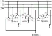
如图4所示,在图3所示的像素单元的实施例的基础上,第一发光元件为第一有机发光二极管OLED1,第二发光元件为第二有机发光二极管OLED2,第三发光元件为第三有机发光二极管OLED3;As shown in FIG. 4 , based on the embodiment of the pixel unit shown in FIG. 3 , the first light-emitting element is the first organic light-emitting diode OLED1 , the second light-emitting element is the second organic light-emitting diode OLED2 , and the third light-emitting element is the third organic light emitting diode OLED3;
所述第一数据写入电路包括第一数据写入晶体管T11;所述第一驱动电路包括第一驱动晶体管T12和第一存储电容C1;所述第一外部补偿检测电路包括第一检测晶体管T13;The first data writing circuit includes a first data writing transistor T11; the first driving circuit includes a first driving transistor T12 and a first storage capacitor C1; the first external compensation detection circuit includes a first detection transistor T13 ;
所述第一数据写入晶体管T11的栅极与所述第一栅线G1连接,所述第一数据写入晶体管T11的漏极与所述第一数据线Data1连接,所述第一数据写入晶体管T11的源极与所述第一驱动晶体管T12的栅极连接;The gate of the first data writing transistor T11 is connected to the first gate line G1, the drain of the first data writing transistor T11 is connected to the first data line Data1, and the first data writing transistor T11 is connected to the first data line Data1. the source of the input transistor T11 is connected to the gate of the first driving transistor T12;
所述第一驱动晶体管T12的漏极与所述输入电源电压VDD的电源电压端连接,所述第一驱动晶体管T12的源极与所述第一有机发光二极管OLED1的阳极连接;OLED1的阴极接地;The drain of the first driving transistor T12 is connected to the power supply voltage terminal of the input power supply voltage VDD, the source of the first driving transistor T12 is connected to the anode of the first organic light emitting diode OLED1; the cathode of OLED1 is grounded ;
所述第一存储电容C1的第一端与所述第一驱动晶体管T12的栅极连接,所述第一存储电容C1的第二端与所述第一驱动晶体管T12的源极连接;The first end of the first storage capacitor C1 is connected to the gate of the first drive transistor T12, and the second end of the first storage capacitor C1 is connected to the source of the first drive transistor T12;
所述第一检测晶体管T13的栅极与所述第一栅线G1连接,所述第一检测晶体管T13的漏极与所述第一驱动晶体管T12的源极连接,所述第一检测晶体管T13的漏极与所述第一外部补偿线Sense1连接;The gate of the first detection transistor T13 is connected to the first gate line G1, the drain of the first detection transistor T13 is connected to the source of the first driving transistor T12, and the first detection transistor T13 The drain is connected to the first external compensation line Sense1;
所述第二数据写入电路包括第二数据写入晶体管T21;所述第二驱动电路包括第二驱动晶体管T22和第二存储电容C2;所述第二外部补偿检测电路包括第二检测晶体管T23;The second data writing circuit includes a second data writing transistor T21; the second driving circuit includes a second driving transistor T22 and a second storage capacitor C2; the second external compensation detection circuit includes a second detection transistor T23 ;
所述第二数据写入晶体管T21的栅极与所述第二栅线G2连接,所述第二数据写入晶体管T21的漏极与所述第一数据线Data1连接,所述第二数据写入晶体管T21的源极与所述第二驱动晶体管T22的栅极连接;The gate of the second data writing transistor T21 is connected to the second gate line G2, the drain of the second data writing transistor T21 is connected to the first data line Data1, and the second data writing transistor T21 is connected to the first data line Data1. The source of the input transistor T21 is connected to the gate of the second driving transistor T22;
所述第二驱动晶体管T22的漏极与所述输入电源电压VDD的电源电压端连接,所述第二驱动晶体管T22的源极与所述第二有机发光二极管OLED2的阳极连接;OLED2的阴极接地;The drain of the second driving transistor T22 is connected to the power supply voltage terminal of the input power supply voltage VDD, the source of the second driving transistor T22 is connected to the anode of the second organic light emitting diode OLED2; the cathode of OLED2 is grounded ;
所述第二存储电容C2的第一端与所述第二驱动晶体管T22的栅极连接,所述第二存储电容C2的第二端与所述第二驱动晶体管T22的源极连接;The first end of the second storage capacitor C2 is connected to the gate of the second drive transistor T22, and the second end of the second storage capacitor C2 is connected to the source of the second drive transistor T22;
所述第二检测晶体管T23的栅极与所述第二栅线G2连接,所述第二检测晶体管T23的漏极与所述第二驱动晶体管T22的源极连接,所述第二检测晶体管T23的源极与所述第一外部补偿线Sense1连接;The gate of the second detection transistor T23 is connected to the second gate line G2, the drain of the second detection transistor T23 is connected to the source of the second driving transistor T22, and the second detection transistor T23 The source is connected to the first external compensation line Sense1;
所述第三数据写入电路包括第三数据写入晶体管T31;所述第三驱动电路包括第三驱动晶体管T32和第三存储电容C3;所述第三外部补偿检测电路包括第三检测晶体管T33;The third data writing circuit includes a third data writing transistor T31; the third driving circuit includes a third driving transistor T32 and a third storage capacitor C3; the third external compensation detection circuit includes a third detection transistor T33 ;
所述第三数据写入晶体管T31的栅极与所述第一栅线G1连接,所述第三数据写入晶体管T31的漏极与第二数据线Data2连接,所述第三数据写入晶体管T31的源极与所述第三驱动晶体管T32的栅极连接;The gate of the third data writing transistor T31 is connected to the first gate line G1, the drain of the third data writing transistor T31 is connected to the second data line Data2, and the third data writing transistor The source of T31 is connected to the gate of the third driving transistor T32;
所述第三驱动晶体管T32的漏极与所述输入电源电压VDD的电源电压端连接,所述第三驱动晶体管T32的源极与所述第三有机发光二极管OLED3的阳极连接;OLED3的阴极接地;The drain of the third driving transistor T32 is connected to the power supply voltage terminal of the input power supply voltage VDD, the source of the third driving transistor T32 is connected to the anode of the third organic light emitting diode OLED3; the cathode of OLED3 is grounded ;
所述第三存储电容C3的第一端与所述第三驱动晶体管T32的栅极连接,所述第三存储电容C3的第二端与所述第三驱动晶体管T32的源极连接;The first end of the third storage capacitor C3 is connected to the gate of the third drive transistor T32, and the second end of the third storage capacitor C3 is connected to the source of the third drive transistor T32;
所述第三检测晶体管T33的栅极与所述第一栅线G1连接,所述第三检测晶体管T33的漏极与所述第三驱动晶体管T32的源极连接,所述第三检测晶体管T33的源极与所述第一外部补偿线Sense1连接。The gate of the third detection transistor T33 is connected to the first gate line G1, the drain of the third detection transistor T33 is connected to the source of the third driving transistor T32, and the third detection transistor T33 The source is connected to the first external compensation line Sense1.
在具体实施时,各有机发光二极管的阴极也可以接入低电压或负电压,但不以此为限。During specific implementation, the cathode of each organic light emitting diode may also be connected to a low voltage or a negative voltage, but not limited to this.
在图4所示的像素单元的具体实施例中,三个亚像素电路共用第一外部补偿线Sense1,可以减少外部补偿线的数目,减小像素布局空间,实现高分辨率。In the specific embodiment of the pixel unit shown in FIG. 4 , the three sub-pixel circuits share the first external compensation line Sense1 , which can reduce the number of external compensation lines, reduce the pixel layout space, and achieve high resolution.
在图4所示的像素单元的具体实施例中,所有的晶体管都为n型晶体管,但不以此为限。In the specific embodiment of the pixel unit shown in FIG. 4 , all transistors are n-type transistors, but not limited thereto.
本发明实施例所述的显示面板包括上述的像素单元。The display panel according to the embodiment of the present invention includes the above-mentioned pixel unit.
在具体实施时,所述显示面板包括显示基板,所述像素单元可以设置于所述显示基板上。In a specific implementation, the display panel includes a display substrate, and the pixel units may be disposed on the display substrate.
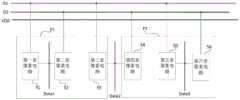
本发明实施例所提供的显示面板可以为手机、平板电脑、电视机、显示器、笔记本电脑、数码相框、导航仪等任何具有显示功能的产品或部件。The display panel provided by the embodiment of the present invention may be any product or component with display function, such as a mobile phone, a tablet computer, a television, a monitor, a notebook computer, a digital photo frame, and a navigator.
本发明实施例所述的显示面板包括像素结构,所述像素结构包括两个上述的像素单元,所述像素单元包括第一亚像素电路、第二亚像素电路和第三亚像素电路;其中,The display panel according to the embodiment of the present invention includes a pixel structure, the pixel structure includes two above-mentioned pixel units, and the pixel unit includes a first sub-pixel circuit, a second sub-pixel circuit and a third sub-pixel circuit; wherein,
第一所述像素单元中的第一亚像素驱动电路分别与第一栅线和第一数据线连接;The first sub-pixel driving circuit in the first described pixel unit is respectively connected with the first gate line and the first data line;
第一所述像素单元中的第二亚像素驱动电路分别与第二栅线和所述第一数据线连接;The second sub-pixel driving circuit in the first pixel unit is respectively connected with the second gate line and the first data line;
第一所述像素单元中的第三亚像素驱动电路分别与第一栅线和第二数据线连接;The third sub-pixel driving circuit in the first pixel unit is connected to the first gate line and the second data line respectively;
第二所述像素单元中的第一亚像素驱动电路分别与第二栅线和第二数据线连接;Second, the first sub-pixel driving circuit in the pixel unit is respectively connected to the second gate line and the second data line;
第二所述像素单元中的第二亚像素驱动电路分别与第一栅线和第三数据线连接;the second sub-pixel driving circuit in the second pixel unit is respectively connected to the first gate line and the third data line;
第二所述像素单元中的第三亚像素驱动电路分别与第二栅线和第三数据线连接。The third sub-pixel driving circuit in the second pixel unit is respectively connected with the second gate line and the third data line.
本发明实施例所述的显示面板中的像素结构包括两个像素单元,每个像素单元包括三个亚像素电路,相邻的两个亚像素电路共用一根数据线,与现有的像素结构相比,本发明实施例所述的显示面板中的像素结构仅需采用三根数据线,从而可以减少采用的数据线的数目,缩小像素布局空间,在有效空间内实现高分辨率,并可以减少源极驱动器的数量,降低产品成本。The pixel structure in the display panel according to the embodiment of the present invention includes two pixel units, each pixel unit includes three sub-pixel circuits, and two adjacent sub-pixel circuits share a data line, which is different from the existing pixel structure. In contrast, the pixel structure in the display panel according to the embodiment of the present invention only needs to use three data lines, thereby reducing the number of data lines used, reducing the pixel layout space, achieving high resolution in the effective space, and reducing The number of source drivers reduces product cost.
本发明实施例提供的像素结构可以为一种采用TOP GATE(顶栅)工艺、顶发射技术的高分辨8K AMOLED(Active-matrix organic light-emitting diode,有源矩阵有机发光二极管)像素结构。The pixel structure provided by the embodiment of the present invention may be a high-resolution 8K AMOLED (Active-matrix organic light-emitting diode) pixel structure using a TOP GATE process and a top emission technology.
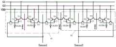
如图5所示,本发明所述的显示面板中的像素结构的一实施例包括第一像素单元P1和第二像素单元P2;As shown in FIG. 5, an embodiment of the pixel structure in the display panel according to the present invention includes a first pixel unit P1 and a second pixel unit P2;
所述第一像素单元P1包括第一亚像素电路51、第二亚像素电路52和第三亚像素电路53;The first pixel unit P1 includes a
所述第二像素单元P2包括第四亚像素电路54、第五亚像素电路55和第六亚像素电路56;The second pixel unit P2 includes a
所述第一亚像素电路51、所述第三亚像素电路53和所述第五亚像素电路55都与第一栅线G1连接;The
所述第二亚像素电路52、所述第四亚像素电路54和所述第六亚像素电路56都与第二栅线G2连接;The
所述第一亚像素电路51和所述第二亚像素电路52都与第一数据线Data1连接;Both the
所述第三亚像素电路53和所述第四亚像素电路54都与第二数据线Data2连接;The
所述第五亚像素电路55和所述第六亚像素电路56都与第三数据线Data3连接。Both the
在图5所示的像素结构的实施例中,所述第一亚像素电路51和所述第二亚像素电路52共用第一数据线Data1;所述第三亚像素电路53和所述第四亚像素电路54共用第二数据线Data2;所述第五亚像素电路55和所述第六亚像素电路56共用第三数据线Data3;可以减少数据线的数目,减小像素布局空间,实现高分辨率,并可以减少采用的源极驱动器的数量,降低生产成本。In the embodiment of the pixel structure shown in FIG. 5 , the
具体的,第一所述像素单元中的第一亚像素驱动电路包括第一外部补偿检测电路、第一数据写入电路和第一驱动电路;第一所述像素单元中的第二亚像素驱动电路包括第二外部补偿检测电路、第二数据写入电路和第二驱动电路;第一所述像素单元中的第三亚像素驱动电路包括第三外部补偿检测电路、第三数据写入电路和第三驱动电路;Specifically, the first sub-pixel driving circuit in the first pixel unit includes a first external compensation detection circuit, a first data writing circuit and a first driving circuit; the second sub-pixel driving circuit in the first pixel unit The circuit includes a second external compensation detection circuit, a second data writing circuit and a second driving circuit; the third sub-pixel driving circuit in the first pixel unit includes a third external compensation detection circuit, a third data writing circuit and a third sub-pixel driving circuit. Three drive circuits;
第二所述像素单元中的第一亚像素驱动电路包括第四外部补偿检测电路、第四数据写入电路和第四驱动电路;第二所述像素单元中的第二亚像素驱动电路包括第五外部补偿检测电路、第五数据写入电路和第五驱动电路;第二所述像素单元中的第三亚像素驱动电路包括第六外部补偿检测电路、第六数据写入电路和第六驱动电路;The first sub-pixel driving circuit in the second pixel unit includes a fourth external compensation detection circuit, a fourth data writing circuit and a fourth driving circuit; the second sub-pixel driving circuit in the second pixel unit includes a Five external compensation detection circuits, fifth data writing circuits and fifth driving circuits; the third sub-pixel driving circuit in the second pixel unit includes a sixth external compensation detection circuit, a sixth data writing circuit and a sixth driving circuit ;
所述第一外部补偿检测电路、所述第二外部补偿检测电路和所述第三外部补偿检测电路都与第一外部补偿线连接;The first external compensation detection circuit, the second external compensation detection circuit and the third external compensation detection circuit are all connected to the first external compensation line;
所述第四外部补偿检测电路、所述第五外部补偿检测电路和所述第六外部补偿检测电路都与第二外部补偿线连接。The fourth external compensation detection circuit, the fifth external compensation detection circuit and the sixth external compensation detection circuit are all connected to the second external compensation line.
在优选情况下,第一个像素单元中的三个亚像素电路共用一根外部补偿线,第二个像素单元中的三个亚像素电路共用一根外部补偿线,以减少采用的外部补偿线的数目。Preferably, the three sub-pixel circuits in the first pixel unit share one external compensation line, and the three sub-pixel circuits in the second pixel unit share one external compensation line, so as to reduce the use of external compensation lines Number of.
如图6所示,本发明所述的显示面板中的像素结构的另一实施例包括第一像素单元P1和第二像素单元P2;As shown in FIG. 6, another embodiment of the pixel structure in the display panel according to the present invention includes a first pixel unit P1 and a second pixel unit P2;
所述第一像素单元P1包括第一亚像素电路51、第二亚像素电路52和第三亚像素电路53;The first pixel unit P1 includes a
所述第二像素单元P2包括第四亚像素电路54、第五亚像素电路55和第六亚像素电路56;The second pixel unit P2 includes a
所述第一亚像素电路51、所述第三亚像素电路53和所述第五亚像素电路55都与第一栅线G1连接;The
所述第二亚像素电路52、所述第四亚像素电路54和所述第六亚像素电路56都与第二栅线G2连接;The
所述第一亚像素电路51和所述第二亚像素电路52都与第一数据线Data1连接;Both the
所述第三亚像素电路53和所述第四亚像素电路54都与第二数据线Data2连接;The
所述第五亚像素电路55和所述第六亚像素电路56都与第三数据线Data3连接;The
所述第一亚像素电路51、所述第二亚像素电路52和所述第三亚像素电路53都与第一外部检测线Sense1连接;The
所述第四亚像素电路54、所述第五亚像素电路55和所述第六亚像素电路56都与第二外部检测线Sense2连接。The
在图6所示的像素结构的实施例中,所述第一亚像素电路51和所述第二亚像素电路52共用第一数据线Data1;所述第三亚像素电路53和所述第四亚像素电路54共用第二数据线Data2;所述第五亚像素电路55和所述第六亚像素电路56共用第三数据线Data3;所述第一亚像素电路51、所述第二亚像素电路52和所述第三亚像素电路53共用第一外部补偿线Sense1,所述第四亚像素电路54、所述第五亚像素电路55和所述第六亚像素电路56共用第二外部补偿线Sense2,可以减少数据线的数目和外部补偿线的数目,减小像素布局空间,实现高分辨率,并可以减少采用的源极驱动器的数量,降低生产成本。In the embodiment of the pixel structure shown in FIG. 6 , the
如图7所示,本发明所述的显示面板中的像素结构的一具体实施例包括第一像素单元和第二像素单元;所述第一像素单元包括第一亚像素电路、第二亚像素电路和第三亚像素电路;所述第二像素单元P2包括第四亚像素电路、第五亚像素电路和第六亚像素电路;As shown in FIG. 7 , a specific embodiment of the pixel structure in the display panel according to the present invention includes a first pixel unit and a second pixel unit; the first pixel unit includes a first sub-pixel circuit, a second sub-pixel a circuit and a third sub-pixel circuit; the second pixel unit P2 includes a fourth sub-pixel circuit, a fifth sub-pixel circuit and a sixth sub-pixel circuit;
所述第一亚像素电路包括第一亚像素驱动电路和第一有机发光二极管OLED1;所述第二亚像素电路包括第二亚像素驱动电路和第二有机发光二极管OLED2;所述第三亚像素电路包括第三亚像素驱动电路和第三有机发光二极管OLED3;所述第四亚像素电路包括第四亚像素驱动电路和第四有机发光二极管OLED4;所述第五亚像素电路包括第五亚像素驱动电路和第五有机发光二极管OLED5;所述第六亚像素电路包括第六亚像素驱动电路和第六有机发光二极管OLED6;The first sub-pixel circuit includes a first sub-pixel driving circuit and a first organic light-emitting diode OLED1; the second sub-pixel circuit includes a second sub-pixel driving circuit and a second organic light-emitting diode OLED2; the third sub-pixel circuit It includes a third sub-pixel driving circuit and a third organic light emitting diode OLED3; the fourth sub-pixel circuit includes a fourth sub-pixel driving circuit and a fourth organic light emitting diode OLED4; the fifth sub-pixel circuit includes a fifth sub-pixel driving circuit and a fifth organic light emitting diode OLED5; the sixth sub-pixel circuit includes a sixth sub-pixel driving circuit and a sixth organic light emitting diode OLED6;
所述第一亚像素驱动电路包括第一数据写入晶体管T11、第一驱动晶体管T12、第一存储电容C1和第一检测晶体管T13;The first sub-pixel driving circuit includes a first data writing transistor T11, a first driving transistor T12, a first storage capacitor C1 and a first detection transistor T13;
T11的栅极与第一栅线G1连接,T11的漏极与所述第一数据线Data1连接,T11的源极与T12的栅极连接;The gate of T11 is connected to the first gate line G1, the drain of T11 is connected to the first data line Data1, and the source of T11 is connected to the gate of T12;
T12的漏极与输入电源电压VDD的电源电压端连接,T12的源极与OLED1的阳极连接;OLED1的阴极接地;The drain of T12 is connected to the power supply voltage terminal of the input power supply voltage VDD, the source of T12 is connected to the anode of OLED1; the cathode of OLED1 is grounded;
C1的第一端与T12的栅极连接,C1的第二端与T12的源极连接;The first end of C1 is connected to the gate of T12, and the second end of C1 is connected to the source of T12;
T13的栅极与所述第一栅线G1连接,T13的漏极与所述T12的源极连接,T13的漏极与所述第一外部补偿线Sense1连接;The gate of T13 is connected to the first gate line G1, the drain of T13 is connected to the source of T12, and the drain of T13 is connected to the first external compensation line Sense1;
所述第二亚像素驱动电路包括第二数据写入晶体管T21、第二驱动晶体管T22、第二存储电容C2和第二检测晶体管T23;The second sub-pixel driving circuit includes a second data writing transistor T21, a second driving transistor T22, a second storage capacitor C2 and a second detection transistor T23;
T21的栅极与所述第二栅线G2连接,T21的漏极与所述第一数据线Data1连接,T21的源极与T22的栅极连接;The gate of T21 is connected to the second gate line G2, the drain of T21 is connected to the first data line Data1, and the source of T21 is connected to the gate of T22;
T22的漏极与所述输入电源电压VDD的电源电压端连接,T22的源极与OLED2的阳极连接;OLED2的阴极接地;The drain of T22 is connected to the power supply voltage terminal of the input power supply voltage VDD, the source of T22 is connected to the anode of OLED2; the cathode of OLED2 is grounded;
C2的第一端与T22的栅极连接,C2的第二端与T22的源极连接;The first end of C2 is connected to the gate of T22, and the second end of C2 is connected to the source of T22;
T23的栅极与所述第二栅线G2连接,T23的漏极与T22的源极连接,T23的源极与所述第一外部补偿线Sense1连接;The gate of T23 is connected to the second gate line G2, the drain of T23 is connected to the source of T22, and the source of T23 is connected to the first external compensation line Sense1;
所述第三亚像素驱动电路包括第三数据写入晶体管T31、第三驱动晶体管T32、第三存储电容C3和第三检测晶体管T33;The third sub-pixel driving circuit includes a third data writing transistor T31, a third driving transistor T32, a third storage capacitor C3 and a third detecting transistor T33;
T31的栅极与所述第一栅线G1连接,T31的漏极与第二数据线Data2连接,T31的源极与T32的栅极连接;The gate of T31 is connected to the first gate line G1, the drain of T31 is connected to the second data line Data2, and the source of T31 is connected to the gate of T32;
T32的漏极与所述输入电源电压VDD的电源电压端连接,T32的源极与OLED3的阳极连接;OLED3的阴极接地;The drain of T32 is connected to the power supply voltage terminal of the input power supply voltage VDD, the source of T32 is connected to the anode of OLED3; the cathode of OLED3 is grounded;
C3的第一端与T32的栅极连接,C3的第二端与T32的源极连接;The first end of C3 is connected to the gate of T32, and the second end of C3 is connected to the source of T32;
T33的栅极与所述第一栅线G1连接,T33的漏极与T32的源极连接,T33的源极与所述第一外部补偿线Sense1连接;The gate of T33 is connected to the first gate line G1, the drain of T33 is connected to the source of T32, and the source of T33 is connected to the first external compensation line Sense1;
所述第四亚像素驱动电路包括第四数据写入晶体管T41、第四驱动晶体管T42、第四存储电容C4和第四检测晶体管T43;The fourth sub-pixel driving circuit includes a fourth data writing transistor T41, a fourth driving transistor T42, a fourth storage capacitor C4 and a fourth detecting transistor T43;
T41的栅极与第二栅线G1连接,T11的漏极与所述第二数据线Data2连接,T41的源极与T42的栅极连接;The gate of T41 is connected to the second gate line G1, the drain of T11 is connected to the second data line Data2, and the source of T41 is connected to the gate of T42;
T42的漏极与输入电源电压VDD的电源电压端连接,T42的源极与OLED4的阳极连接;OLED4的阴极接地;The drain of T42 is connected to the power supply voltage terminal of the input power supply voltage VDD, the source of T42 is connected to the anode of OLED4; the cathode of OLED4 is grounded;
C4的第一端与T42的栅极连接,C4的第二端与T42的源极连接;The first end of C4 is connected to the gate of T42, and the second end of C4 is connected to the source of T42;
T43的栅极与所述第二栅线G2连接,T43的漏极与所述T42的源极连接,T43的漏极与所述第二外部补偿线Sense2连接;The gate of T43 is connected to the second gate line G2, the drain of T43 is connected to the source of T42, and the drain of T43 is connected to the second external compensation line Sense2;
所述第五亚像素驱动电路包括第五数据写入晶体管T51、第五驱动晶体管T52、第五存储电容C5和第五检测晶体管T53;The fifth sub-pixel driving circuit includes a fifth data writing transistor T51, a fifth driving transistor T52, a fifth storage capacitor C5 and a fifth detecting transistor T53;
T51的栅极与所述第一栅线G1连接,T51的漏极与所述第三数据线Data3连接,T51的源极与T52的栅极连接;The gate of T51 is connected to the first gate line G1, the drain of T51 is connected to the third data line Data3, and the source of T51 is connected to the gate of T52;
T52的漏极与所述输入电源电压VDD的电源电压端连接,T52的源极与OLED5的阳极连接;OLED5的阴极接地;The drain of T52 is connected to the power supply voltage terminal of the input power supply voltage VDD, the source of T52 is connected to the anode of OLED5; the cathode of OLED5 is grounded;
C5的第一端与T52的栅极连接,C5的第二端与T52的源极连接;The first end of C5 is connected to the gate of T52, and the second end of C5 is connected to the source of T52;
T53的栅极与所述第一栅线G1连接,T53的漏极与T52的源极连接,T53的源极与所述第二外部补偿线Sense2连接;The gate of T53 is connected to the first gate line G1, the drain of T53 is connected to the source of T52, and the source of T53 is connected to the second external compensation line Sense2;
所述第六亚像素驱动电路包括第六数据写入晶体管T61、第六驱动晶体管T62、第六存储电容C6和第六检测晶体管T63;The sixth sub-pixel driving circuit includes a sixth data writing transistor T61, a sixth driving transistor T62, a sixth storage capacitor C6 and a sixth detection transistor T63;
T61的栅极与所述第二栅线G2连接,T61的漏极与第三数据线Data3连接,T61的源极与T62的栅极连接;The gate of T61 is connected to the second gate line G2, the drain of T61 is connected to the third data line Data3, and the source of T61 is connected to the gate of T62;
T62的漏极与所述输入电源电压VDD的电源电压端连接,T62的源极与OLED6的阳极连接;OLED6的阴极接地;The drain of T62 is connected to the power supply voltage terminal of the input power supply voltage VDD, the source of T62 is connected to the anode of OLED6; the cathode of OLED6 is grounded;
C6的第一端与T62的栅极连接,C6的第二端与T62的源极连接;The first end of C6 is connected to the gate of T62, and the second end of C6 is connected to the source of T62;
T63的栅极与所述第二栅线G2连接,T63的漏极与T62的源极连接,T63的源极与所述第二外部补偿线Sense2连接。The gate of T63 is connected to the second gate line G2, the drain of T63 is connected to the source of T62, and the source of T63 is connected to the second external compensation line Sense2.
在图7所示的像素结构的具体实施例中,第一亚像素电路为第一红色亚像素电路,OLED1为第一红色OLED;第二亚像素电路为第一绿色亚像素电路,OLED2为第一绿色OLED;第三亚像素电路为第一蓝色亚像素电路,OLED3为第一蓝色OLED;第四亚像素电路为第二红色亚像素电路,OLED4为第二红色OLED;第五亚像素电路为第二绿色亚像素电路,OLED5为第二绿色OLED;第六亚像素电路为第二蓝色亚像素电路,OLED6为第二蓝色OLED。In the specific embodiment of the pixel structure shown in FIG. 7 , the first sub-pixel circuit is a first red sub-pixel circuit, and OLED1 is a first red OLED; the second sub-pixel circuit is a first green sub-pixel circuit, and OLED2 is a first green sub-pixel circuit. A green OLED; the third sub-pixel circuit is the first blue sub-pixel circuit, OLED3 is the first blue OLED; the fourth sub-pixel circuit is the second red sub-pixel circuit, OLED4 is the second red OLED; the fifth sub-pixel circuit is a second green sub-pixel circuit, and OLED5 is a second green OLED; the sixth sub-pixel circuit is a second blue sub-pixel circuit, and OLED6 is a second blue OLED.
在图7所示的像素结构的具体实施例中,所有的晶体管都为n型晶体管,但不以此为限。In the specific embodiment of the pixel structure shown in FIG. 7 , all transistors are n-type transistors, but not limited thereto.
本发明如图7所示的像素结构的具体实施例在进行显示驱动时,显示周期包括第一显示时间段和第二显示时间段;In the specific embodiment of the pixel structure shown in FIG. 7 of the present invention, when display driving is performed, the display period includes a first display period and a second display period;
在所述第一显示时间段,第一数据线Data1输出第一数据电压Vdata1,第二数据线Data2输出第二数据电压Vdata2,第三数据线Data3输出第三数据电压Vdata3,在第一栅线G1的控制下,第一亚像素驱动电路根据Vdata1驱动OLED1,第三亚像素驱动电路根据Vdata2驱动OLED3,第五亚像素驱动电路根据Vdata3驱动OLED5;During the first display period, the first data line Data1 outputs the first data voltage Vdata1, the second data line Data2 outputs the second data voltage Vdata2, and the third data line Data3 outputs the third data voltage Vdata3. Under the control of G1, the first sub-pixel driving circuit drives OLED1 according to Vdata1, the third sub-pixel driving circuit drives OLED3 according to Vdata2, and the fifth sub-pixel driving circuit drives OLED5 according to Vdata3;
在所述第二显示时间段,第一数据线Data1输出第四数据电压Vdata4,第二数据线Data2输出第五数据电压Vdata5,第三数据线Data3输出第六数据电压Vdata6,在第二栅线G2的控制下,第二亚像素驱动电路根据Vdata4驱动OLED2,第四亚像素驱动电路根据Vdata5驱动OLED4,第六亚像素驱动电路根据Vdata6驱动OLED6。During the second display period, the first data line Data1 outputs the fourth data voltage Vdata4, the second data line Data2 outputs the fifth data voltage Vdata5, the third data line Data3 outputs the sixth data voltage Vdata6, and the second gate line outputs the sixth data voltage Vdata6. Under the control of G2, the second sub-pixel driving circuit drives OLED2 according to Vdata4, the fourth sub-pixel driving circuit drives OLED4 according to Vdata5, and the sixth sub-pixel driving circuit drives OLED6 according to Vdata6.
在具体实施时,所述第一显示时间段可以包括第一显示阶段、第三显示阶段和第五显示阶段;所述第二显示时间段可以包括第二显示阶段、第四显示阶段和第六显示阶段;In a specific implementation, the first display period may include a first display period, a third display period, and a fifth display period; the second display period may include a second display period, a fourth display period, and a sixth display period display stage;
在所述第一显示阶段,Data1输出所述第一数据电压Vdata1,在所述第一栅线G1的控制下,T11打开,以控制将所述第一数据电压Vdata1写入T12的栅极,T12根据其栅极的电压驱动OLED1;In the first display stage, Data1 outputs the first data voltage Vdata1, and under the control of the first gate line G1, T11 is turned on to control writing the first data voltage Vdata1 into the gate of T12, T12 drives OLED1 according to the voltage of its gate;
在所述第二显示阶段,Data2输出所述第五数据电压Vdata5,在所述第二栅线G2的控制下,T41控制将Vdata5写入T42的栅极,T42根据其栅极的电压驱动OLED4;In the second display stage, Data2 outputs the fifth data voltage Vdata5. Under the control of the second gate line G2, T41 controls to write Vdata5 into the gate of T42, and T42 drives OLED4 according to the voltage of its gate. ;
在所述第三显示阶段,Data3输出所述第三数据电压Vdata3,在所述第一栅线G1的控制下,T51打开,以控制将Vdata3写入T52的栅极,T52根据其栅极的电压驱动OLED5;In the third display stage, Data3 outputs the third data voltage Vdata3. Under the control of the first gate line G1, T51 is turned on to control the writing of Vdata3 into the gate of T52. Voltage drive OLED5;
在所述第四显示阶段,Data1输出所述第四数据电压Vdata4,在所述第二栅线G2的控制下,T21打开,以控制将Vdata4写入T22的栅极,T22根据其栅极的电压驱动OLED2;In the fourth display stage, Data1 outputs the fourth data voltage Vdata4, and under the control of the second gate line G2, T21 is turned on to control the writing of Vdata4 into the gate of T22. voltage drive OLED2;
在所述第五显示阶段,Data2输出所述第二数据电压Vdata2,在所述第一栅线G1的控制下,T31打开,以控制将Vdata2写入T32的栅极,T32根据其栅极的电压驱动OLED3;In the fifth display stage, Data2 outputs the second data voltage Vdata2. Under the control of the first gate line G1, T31 is turned on to control the writing of Vdata2 into the gate of T32. Voltage drive OLED3;
在所述第六显示阶段,Data3输出所述第六数据电压Vdata6,在所述第二栅线G2的控制下,T61打开,以控制Vdata6写入T62,T62根据其栅极的电压驱动OLED6。In the sixth display stage, Data3 outputs the sixth data voltage Vdata6, and under the control of the second gate line G2, T61 is turned on to control Vdata6 to write into T62, which drives OLED6 according to the voltage of its gate.
如图8所示,本发明如图7所示的像素结构的具体实施例在显示纯色时,G1和G2交替打开;As shown in FIG. 8 , in the specific embodiment of the pixel structure shown in FIG. 7 of the present invention, when a solid color is displayed, G1 and G2 are turned on alternately;
在第一红色显示时间段t81,G1输入高电平,G2输入低电平,Data1输出第一红色数据电压Vdata_R1,OLED1发红光;In the first red display period t81, G1 inputs a high level, G2 inputs a low level, Data1 outputs the first red data voltage Vdata_R1, and OLED1 emits red light;
在第二红色显示时间段t82,G2输入高电平,G1输入低电平,Data2输出第二红色数据电压Vdata_R2,OLED4发红光;In the second red display period t82, G2 inputs a high level, G1 inputs a low level, Data2 outputs a second red data voltage Vdata_R2, and OLED4 emits red light;
在第一绿色显示时间段t83,G1输入高电平,G2输入低电平,Data3输出第一绿色数据电压Vdata_G1,OLED5发绿光;In the first green display period t83, G1 inputs a high level, G2 inputs a low level, Data3 outputs the first green data voltage Vdata_G1, and OLED5 emits green light;
在第二绿色显示时间段t84,G2输入高电平,G1输入低电平,Data1输出第二绿色数据电压Vdata_G2,OLED2发绿光;In the second green display period t84, G2 inputs a high level, G1 inputs a low level, Data1 outputs a second green data voltage Vdata_G2, and OLED2 emits green light;
在第一蓝色显示时间段t85,G1输入高电平,G2输入低电平,Data2输出第一蓝色数据电压Vdata_B1,OLED3发蓝光;In the first blue display period t85, G1 inputs a high level, G2 inputs a low level, Data2 outputs the first blue data voltage Vdata_B1, and OLED3 emits blue light;
在第二蓝色显示时间段t86,G2输入高电平,G1输入低电平,Data3输出第二蓝色数据电压Vdata_B2,OLED6发蓝光。In the second blue display period t86, G2 inputs a high level, G1 inputs a low level, Data3 outputs a second blue data voltage Vdata_B2, and the OLED6 emits blue light.
在图8中,第一红色显示时间段t81也即所述第一显示阶段,Vdata_R1也即所述第一数据电压Vdata1;所述第二红色显示时间段t82也即所述第二显示阶段,Vdata_R2也即所述第五数据电压Vdata5;所述第一绿色显示时间段t83也即所述第三显示阶段,Vdata_G1也即所述第三数据电压Vdata3;所述第二绿色显示时间段t84也即所述第四显示阶段,Vdata_G2也即所述第四数据电压Vdata4;所述第一蓝色显示时间段t85也即所述第五显示阶段,Vdata_B1也即第二数据电压Vdata2;所述第二蓝色显示时间段t86也即所述第六显示阶段,Vdata_B2也即第六数据电压Vdata6。In FIG. 8, the first red display period t81 is also the first display stage, Vdata_R1 is also the first data voltage Vdata1; the second red display period t82 is also the second display stage, Vdata_R2 is also the fifth data voltage Vdata5; the first green display period t83 is also the third display stage, Vdata_G1 is also the third data voltage Vdata3; the second green display period t84 is also That is, in the fourth display stage, Vdata_G2 is also the fourth data voltage Vdata4; the first blue display period t85 is also the fifth display stage, Vdata_B1 is also the second data voltage Vdata2; The second blue display period t86 is the sixth display stage, and Vdata_B2 is the sixth data voltage Vdata6.
在对本发明实施例所述的显示面板中的像素结构进行外部补偿控制时,可以在一个外部补偿控制时间段对一个亚像素电路进行外部补偿控制,也可以在一个外部补偿控制时间段对两个亚像素电路同时进行外部补偿控制,下面对以上两种情况进行详细介绍。When performing external compensation control on the pixel structure in the display panel according to the embodiment of the present invention, one sub-pixel circuit may be externally compensated and controlled in one external compensation control time period, or two sub-pixel circuits may be externally compensated and controlled in one external compensation control time period. The sub-pixel circuit performs external compensation control at the same time, and the above two cases are described in detail below.
本发明如图7所示的像素结构的具体实施例在进行外部补偿控制时,外部补偿控制周期可以包括六个外部补偿控制时间段,在每个外部补偿控制时间段分别对一个亚像素电路进行外部补偿控制;In the specific embodiment of the pixel structure shown in FIG. 7 of the present invention, when external compensation control is performed, the external compensation control period may include six external compensation control time periods, and one sub-pixel circuit is respectively performed in each external compensation control time period. External compensation control;
在第一外部补偿控制时间段,Data1输出第一红色数据电压Vdata_R1,G1输入高电平,G2输入低电平,T11和T13都打开,以将Vdata_R1输入T12的栅极,并将T12的源极电压写入Sense1,以对第一亚像素电路进行外部补偿控制;During the first external compensation control period, Data1 outputs the first red data voltage Vdata_R1, G1 inputs a high level, G2 inputs a low level, both T11 and T13 are turned on, so that Vdata_R1 is input to the gate of T12, and the source of T12 is The pole voltage is written into Sense1 to perform external compensation control on the first sub-pixel circuit;
在第二外部补偿控制时间段,Data1输出第一绿色数据电压Vdata_G1,G2输入高电平,G1输入低电平,T21和T23都打开,以将Vdata_G1输入T22的栅极,并将T22的源极电压写入Sense1,以对第二亚像素电路进行外部补偿控制;During the second external compensation control period, Data1 outputs the first green data voltage Vdata_G1, G2 inputs a high level, G1 inputs a low level, both T21 and T23 are turned on, so that Vdata_G1 is input to the gate of T22, and the source of T22 is connected to The pole voltage is written into Sense1 to perform external compensation control on the second sub-pixel circuit;
在第三外部补偿控制时间段,Data2输出第一蓝色数据电压Vdata_B1,G1输入高电平,G2输入低电平,T31和T33都打开,以将Vdata_B1输入T32的栅极,并将T32的源极电压写入Sense1,以对第三亚像素电路进行外部补偿控制;During the third external compensation control period, Data2 outputs the first blue data voltage Vdata_B1, G1 inputs a high level, G2 inputs a low level, and both T31 and T33 are turned on, so that Vdata_B1 is input to the gate of T32, and T32’s gate is turned on. The source voltage is written into Sense1 to perform external compensation control for the third sub-pixel circuit;
在第四外部补偿控制时间段,Data2输出第二红色数据电压Vdata_R2,G2输入高电平,G1输入低电平,T41和T43都打开,以将Vdata_R2输入T42的栅极,并将T42的源极电压写入Sense2,以对第四亚像素电路进行外部补偿控制;During the fourth external compensation control period, Data2 outputs the second red data voltage Vdata_R2, G2 inputs a high level, G1 inputs a low level, and both T41 and T43 are turned on to input Vdata_R2 to the gate of T42 and to the source of T42 The pole voltage is written into Sense2 to perform external compensation control on the fourth sub-pixel circuit;
在第五外部补偿控制时间段,Data3输出第二绿色数据电压Vdata_G2,G1输入高电平,G2输入低电平,T51和T53都打开,以将Vdata_G2输入T52的栅极,并将T52的源极电压写入Sense2,以对第五亚像素电路进行外部补偿控制;During the fifth external compensation control period, Data3 outputs the second green data voltage Vdata_G2, G1 inputs a high level, G2 inputs a low level, and both T51 and T53 are turned on to input Vdata_G2 to the gate of T52, and to input the source of T52 to The pole voltage is written into Sense2 to perform external compensation control on the fifth sub-pixel circuit;
在第六外部补偿控制时间段,Data3输出第二蓝色数据电压Vdata_B2,G2输入高电平,G1输入低电平,T61和T63都打开,以将Vdata_B2输入T62的栅极,并将T62的源极电压写入Sense2,以对第六亚像素电路进行外部补偿控制。During the sixth external compensation control period, Data3 outputs the second blue data voltage Vdata_B2, G2 inputs a high level, G1 inputs a low level, and both T61 and T63 are turned on to input Vdata_B2 to the gate of T62, and to input the gate of T62 to The source voltage is written into Sense2 for external compensation control of the sixth sub-pixel circuit.
本发明如图7所示的像素结构的具体实施例在进行外部补偿控制时,可以依次对一种颜色的亚像素电路进行外部补偿控制,例如,可以依次对第一亚像素电路和第四亚像素电路(所述第一亚像素电路和所述第四亚像素电路都为红色亚像素电路)进行外部补偿控制;In the specific embodiment of the pixel structure shown in FIG. 7 of the present invention, when performing external compensation control, the external compensation control can be performed on the sub-pixel circuits of one color in sequence. For example, the first sub-pixel circuit and the fourth sub-pixel circuit can be sequentially controlled. The pixel circuit (both the first sub-pixel circuit and the fourth sub-pixel circuit are red sub-pixel circuits) performs external compensation control;
如图9所示,在第一时间段T1,G1输入高电平,G2输入低电平,Data1输出第一红色数据电压Vdata_R1,T11和T13都打开,以将Vdata_R1输入T12的栅极,并将T12的源极电压写入Sense1,以对第一亚像素电路进行外部补偿控制;As shown in FIG. 9 , in the first time period T1, G1 inputs a high level, G2 inputs a low level, Data1 outputs the first red data voltage Vdata_R1, both T11 and T13 are turned on to input Vdata_R1 to the gate of T12, and Write the source voltage of T12 into Sense1 to perform external compensation control on the first sub-pixel circuit;
在第二时间段T2,G2输入高电平,G1输入低电平,Data2输出第二红色数据电压Vdata_R2,T41和T43都打开,以将Vdata_R2输入T42的栅极,并将T42的源极电压写入Sense2,以对第四亚像素电路进行外部补偿控制;In the second time period T2, G2 inputs a high level, G1 inputs a low level, Data2 outputs a second red data voltage Vdata_R2, both T41 and T43 are turned on to input Vdata_R2 to the gate of T42, and to input the source voltage of T42 Write Sense2 to perform external compensation control on the fourth sub-pixel circuit;
在图9中,标号为T3的为第三时间段。In FIG. 9, the third time period is labeled T3.
本发明如图7所示的像素结构的具体实施例在进行外部补偿控制时,可以在一个外部补偿控制时间段内对第一亚像素电路和第五亚像素电路同时进行外部补偿控制;In the specific embodiment of the pixel structure shown in FIG. 7 of the present invention, when performing external compensation control, the first sub-pixel circuit and the fifth sub-pixel circuit can be simultaneously externally compensated and controlled within an external compensation control time period;
如图10所示,在一外部补偿控制时间段T0,Data1输出第一红色数据电压Vdata_R1,Data3输入第二绿色数据电压Vdata_G2,G1输入高电平,G2输入低电平,T11和T13都打开,以将Vdata_R1写入T12的栅极,并将T12的源极电压写入Sense1,以对第一亚像素电路进行外部补偿控制;T51和T53都打开,以将Vdata_G2写入T52的栅极,并将T52的源极电压写入Sense2;以在该外部补偿控制时间段T0同时对第一亚像素电路和第五亚像素电路进行外部补偿控制,从而可以提升外部补偿速度,从而提升补偿能力;As shown in FIG. 10, during an external compensation control period T0, Data1 outputs the first red data voltage Vdata_R1, Data3 inputs the second green data voltage Vdata_G2, G1 inputs a high level, G2 inputs a low level, and both T11 and T13 are turned on. , to write Vdata_R1 to the gate of T12, and write the source voltage of T12 to Sense1 to perform external compensation control on the first sub-pixel circuit; both T51 and T53 are turned on to write Vdata_G2 to the gate of T52, Write the source voltage of T52 into Sense2; to perform external compensation control on the first sub-pixel circuit and the fifth sub-pixel circuit at the same time during the external compensation control period T0, so that the external compensation speed can be improved, thereby improving the compensation capability;
在所述外部补偿控制时间段T0,Data2输出关断控制电压,G1输入高电平,G2输入低电平,T31和T33都打开,已将关断控制电压写入T32的栅极,从而控制T32关断,由于T32的源极与T12的源极同时与Sense1连接,为了使得第三亚像素电路不会影响Sense1上的电压,需要在所述外部补偿控制时间段T0控制T32关断。During the external compensation control period T0, Data2 outputs the turn-off control voltage, G1 inputs a high level, G2 inputs a low level, both T31 and T33 are turned on, and the turn-off control voltage has been written to the gate of T32, thereby controlling T32 is turned off. Since the source of T32 and the source of T12 are connected to Sense1 at the same time, in order to prevent the third sub-pixel circuit from affecting the voltage on Sense1, it is necessary to control T32 to be turned off during the external compensation control period T0.
本发明如图7所示的像素结构的具体实施例在进行外部补偿控制时,可以在一个外部补偿控制时间段内对第三亚像素电路和第五亚像素电路同时进行外部补偿控制;In the specific embodiment of the pixel structure shown in FIG. 7 of the present invention, when performing external compensation control, the third sub-pixel circuit and the fifth sub-pixel circuit can be simultaneously externally compensated and controlled within an external compensation control time period;
如图11所示,在一外部补偿控制时间段T0,Data2输出第一蓝色数据电压Vdata_B1,Data3输入第二绿色数据电压Vdata_G2,G1输入高电平,G2输入低电平,T31和T33都打开,以将Vdata_B1写入T32的栅极,并将T32的源极电压写入Sense1,以对第三亚像素电路进行外部补偿控制;T51和T53都打开,以将Vdata_G2写入T52的栅极,并将T52的源极电压写入Sense2;以在该外部补偿控制时间段T0同时对第三亚像素电路和第五亚像素电路进行外部补偿控制,从而可以提升外部补偿速度,从而提升补偿能力;As shown in FIG. 11, during an external compensation control period T0, Data2 outputs a first blue data voltage Vdata_B1, Data3 inputs a second green data voltage Vdata_G2, G1 inputs a high level, G2 inputs a low level, both T31 and T33 Turn on to write Vdata_B1 to the gate of T32 and write the source voltage of T32 to Sense1 for external compensation control of the third sub-pixel circuit; both T51 and T53 are turned on to write Vdata_G2 to the gate of T52, Write the source voltage of T52 into Sense2; to perform external compensation control on the third sub-pixel circuit and the fifth sub-pixel circuit at the same time during the external compensation control period T0, so that the external compensation speed can be improved, thereby improving the compensation capability;
在所述外部补偿控制时间段T0,Data1输出关断控制电压,G1输入高电平,G2输入低电平,T11和T13都打开,已将关断控制电压写入T12的栅极,从而控制T12关断,由于T32的源极与T12的源极同时与Sense1连接,为了使得第一亚像素电路不会影响Sense1上的电压,需要在所述外部补偿控制时间段T0控制T12关断。During the external compensation control period T0, Data1 outputs the turn-off control voltage, G1 inputs a high level, G2 inputs a low level, both T11 and T13 are turned on, and the turn-off control voltage has been written to the gate of T12, thereby controlling T12 is turned off. Since the source of T32 and the source of T12 are connected to Sense1 at the same time, in order to prevent the first sub-pixel circuit from affecting the voltage on Sense1, it is necessary to control T12 to be turned off during the external compensation control period T0.
本发明如图7所示的像素结构的具体实施例在进行外部补偿控制时,可以在一个外部补偿控制时间段内对第二亚像素电路和第四亚像素电路同时进行外部补偿控制;In the specific embodiment of the pixel structure shown in FIG. 7 of the present invention, when performing external compensation control, the second sub-pixel circuit and the fourth sub-pixel circuit can be simultaneously externally compensated and controlled within an external compensation control time period;
如图12所示,在一外部补偿控制时间段T0,Data1输出第一绿色数据电压Vdata_G1,Data2输入第二红色数据电压Vdata_R2,G1输入低电平,G2输入高电平,T21和T23都打开,以将Vdata_G1写入T22的栅极,并将T22的源极电压写入Sense1,以对第二亚像素电路进行外部补偿控制;T41和T43都打开,以将Vdata_R2写入T42的栅极,并将T42的源极电压写入Sense2;以在该外部补偿控制时间段T0同时对第二亚像素电路和第四亚像素电路进行外部补偿控制,从而可以提升外部补偿速度,从而提升补偿能力;As shown in FIG. 12, during an external compensation control period T0, Data1 outputs the first green data voltage Vdata_G1, Data2 inputs the second red data voltage Vdata_R2, G1 inputs a low level, G2 inputs a high level, and both T21 and T23 are turned on. , to write Vdata_G1 to the gate of T22, and write the source voltage of T22 to Sense1 to perform external compensation control for the second sub-pixel circuit; both T41 and T43 are turned on to write Vdata_R2 to the gate of T42, Write the source voltage of T42 into Sense2; to perform external compensation control on the second sub-pixel circuit and the fourth sub-pixel circuit at the same time during the external compensation control period T0, so that the external compensation speed can be improved, thereby improving the compensation capability;
在所述外部补偿控制时间段T0,Data3输出关断控制电压,G2输入高电平,G1输入低电平,T61和T63都打开,已将关断控制电压写入T62的栅极,从而控制T62关断,由于T62的源极与T42的源极同时与Sense2连接,为了使得第四亚像素电路不会影响Sense2上的电压,需要在所述外部补偿控制时间段T0控制T62关断。During the external compensation control period T0, Data3 outputs the turn-off control voltage, G2 inputs a high level, G1 inputs a low level, both T61 and T63 are turned on, and the turn-off control voltage has been written to the gate of T62, thereby controlling T62 is turned off. Since the source of T62 and the source of T42 are connected to Sense2 at the same time, in order to prevent the fourth sub-pixel circuit from affecting the voltage on Sense2, it is necessary to control T62 to be turned off during the external compensation control period T0.
本发明如图7所示的像素结构的具体实施例在进行外部补偿控制时,可以在一个外部补偿控制时间段内对第二亚像素电路和第六亚像素电路同时进行外部补偿控制;In the specific embodiment of the pixel structure shown in FIG. 7 of the present invention, when performing external compensation control, the second sub-pixel circuit and the sixth sub-pixel circuit can be simultaneously externally compensated and controlled within an external compensation control time period;
如图13所示,在一外部补偿控制时间段T0,Data1输出第一绿色数据电压Vdata_G1,Data2输入第二蓝色数据电压Vdata_B2,G1输入低电平,G2输入高电平,T21和T23都打开,以将Vdata_G1写入T22的栅极,并将T22的源极电压写入Sense1,以对第二亚像素电路进行外部补偿控制;T61和T63都打开,以将Vdata_B2写入T62的栅极,并将T62的源极电压写入Sense2;以在该外部补偿控制时间段T0同时对第二亚像素电路和第六亚像素电路进行外部补偿控制,从而可以提升外部补偿速度,从而提升补偿能力;As shown in FIG. 13, during an external compensation control period T0, Data1 outputs a first green data voltage Vdata_G1, Data2 inputs a second blue data voltage Vdata_B2, G1 inputs a low level, G2 inputs a high level, both T21 and T23 Open to write Vdata_G1 to the gate of T22 and write the source voltage of T22 to Sense1 for external compensation control of the second sub-pixel circuit; both T61 and T63 are open to write Vdata_B2 to the gate of T62 , and write the source voltage of T62 into Sense2; to perform external compensation control on the second sub-pixel circuit and the sixth sub-pixel circuit at the same time during the external compensation control period T0, so that the external compensation speed can be improved, thereby improving the compensation capability. ;
在所述外部补偿控制时间段T0,Data2输出关断控制电压,G2输入高电平,G1输入低电平,T41和T43都打开,已将关断控制电压写入T42的栅极,从而控制T42关断,由于T62的源极与T42的源极同时与Sense2连接,为了使得第四亚像素电路不会影响Sense2上的电压,需要在所述外部补偿控制时间段T0控制T42关断。During the external compensation control period T0, Data2 outputs the turn-off control voltage, G2 inputs a high level, G1 inputs a low level, both T41 and T43 are turned on, and the turn-off control voltage has been written to the gate of T42, thereby controlling T42 is turned off. Since the source of T62 and the source of T42 are connected to Sense2 at the same time, in order to prevent the fourth sub-pixel circuit from affecting the voltage on Sense2, it is necessary to control T42 to be turned off during the external compensation control period T0.
在本发明具体实施例中,由于像素结构中的各晶体管都为n型晶体管,因此关断控制电压可以为负电压、低电压或零,以控制相应的栅极接入该关断控制电压的驱动晶体管关断,但不以此为限。In the specific embodiment of the present invention, since each transistor in the pixel structure is an n-type transistor, the turn-off control voltage can be a negative voltage, a low voltage or zero, so as to control the corresponding gate to be connected to the turn-off control voltage. The driving transistor is turned off, but not limited thereto.
本发明实施例所述的显示面板的驱动方法,应用于上述的显示面板,显示周期包括第一显示时间段和第二显示时间段;所述显示面板的驱动方法包括:The driving method of the display panel according to the embodiment of the present invention is applied to the above-mentioned display panel, and the display period includes a first display time period and a second display time period; the driving method of the display panel includes:
在所述第一显示时间段,第一数据线输出第一数据电压,第二数据线输出第二数据电压,第三数据线输出第三数据电压,在第一栅线的控制下,第一所述像素单元中的第一亚像素驱动电路根据所述第一数据电压驱动第一所述像素单元中的第一发光元件,第一所述像素单元中的第三亚像素驱动电路根据所述第二数据电压驱动第一所述像素单元中的第三发光元件,第二所述像素单元中的第二亚像素驱动电路根据所述第三数据电压驱动第二所述像素单元中的第二发光元件;During the first display period, the first data line outputs the first data voltage, the second data line outputs the second data voltage, and the third data line outputs the third data voltage. Under the control of the first gate line, the first data line outputs the first data voltage. The first sub-pixel drive circuit in the pixel unit drives the first light-emitting element in the first pixel unit according to the first data voltage, and the third sub-pixel drive circuit in the first pixel unit drives according to the first data voltage. Two data voltages drive the third light-emitting element in the first pixel unit, and the second sub-pixel driving circuit in the second pixel unit drives the second light-emitting element in the second pixel unit according to the third data voltage element;
在所述第二显示时间段,第二数据线输出第四数据电压,第二数据线输出第五数据电压,第三数据线输出第六数据电压,在第二栅线的控制下,第一所述像素单元中的第二亚像素驱动电路根据所述第四数据电压驱动第一所述像素单元中的第二发光元件,第二所述像素单元中的第一亚像素驱动电路根据所述第五数据电压驱动第二所述像素单元中的第一发光元件,第二所述像素单元中的第三亚像素驱动电路根据所述第六数据电压驱动第二所述像素单元中的第三发光元件。During the second display period, the second data line outputs the fourth data voltage, the second data line outputs the fifth data voltage, and the third data line outputs the sixth data voltage. Under the control of the second gate line, the first The second sub-pixel driving circuit in the pixel unit drives the second light-emitting element in the first pixel unit according to the fourth data voltage, and the first sub-pixel driving circuit in the second pixel unit according to the The fifth data voltage drives the first light-emitting element in the second pixel unit, and the third sub-pixel driving circuit in the second pixel unit drives the third light-emitting element in the second pixel unit according to the sixth data voltage element.
在具体实施时,可以将显示周期分为两个显示时间段,在第一显示时间段对第一像素单元中的第一亚像素电路、第一像素单元中的第三亚像素电路和第二像素单元中的第二亚像素电路进行显示驱动,在第二显示时间段,对第一像素单元中的第二亚像素电路、第二像素单元中的第一亚像素电路和第二像素单元中的第三亚像素电路进行显示驱动。In specific implementation, the display period can be divided into two display time periods, and in the first display time period, the first sub-pixel circuit in the first pixel unit, the third sub-pixel circuit in the first pixel unit and the second pixel The second sub-pixel circuit in the unit performs display driving, and in the second display period, the second sub-pixel circuit in the first pixel unit, the first sub-pixel circuit in the second pixel unit, and the second pixel unit are driven. The third sub-pixel circuit performs display driving.
具体的,第一所述像素单元中的第一亚像素驱动电路包括第一数据写入电路和第一驱动电路;第一所述像素单元中的第二亚像素驱动电路包括第二数据写入电路和第二驱动电路;第一所述像素单元中的第三亚像素驱动电路包括第三数据写入电路和第三驱动电路;第二所述像素单元中的第一亚像素驱动电路包括第四数据写入电路和第四驱动电路;第二所述像素单元中的第二亚像素驱动电路包括第五数据写入电路和第五驱动电路;第二所述像素单元中的第三亚像素驱动电路包括第六数据写入电路和第六驱动电路;所述第一显示时间段可以包括第一显示阶段、第三显示阶段和第五显示阶段;所述第二显示时间段可以包括第二显示阶段、第四显示阶段和第六显示阶段;Specifically, the first sub-pixel driving circuit in the first pixel unit includes a first data writing circuit and a first driving circuit; the second sub-pixel driving circuit in the first pixel unit includes a second data writing circuit circuit and a second driving circuit; the third sub-pixel driving circuit in the first pixel unit includes a third data writing circuit and a third driving circuit; the first sub-pixel driving circuit in the second pixel unit includes a fourth a data writing circuit and a fourth driving circuit; the second sub-pixel driving circuit in the second pixel unit includes a fifth data writing circuit and a fifth driving circuit; the third sub-pixel driving circuit in the second pixel unit including a sixth data writing circuit and a sixth driving circuit; the first display period may include a first display stage, a third display stage and a fifth display stage; the second display period may include a second display stage , the fourth display stage and the sixth display stage;
所述显示面板的驱动方法可以包括:The driving method of the display panel may include:
在所述第一显示阶段,所述第一数据线输出所述第一数据电压,在所述第一栅线的控制下,所述第一数据写入电路控制将所述第一数据电压写入所述第一驱动电路的控制端,所述第一驱动电路根据其控制端的电压驱动第一所述像素单元中的第一发光元件;In the first display stage, the first data line outputs the first data voltage, and under the control of the first gate line, the first data writing circuit controls to write the first data voltage into the control terminal of the first driving circuit, and the first driving circuit drives the first light-emitting element in the first pixel unit according to the voltage of the control terminal;
在所述第二显示阶段,所述第二数据线输出所述第五数据电压,在所述第二栅线的控制下,所述第四数据写入电路控制将所述第五数据电压写入所述第四驱动电路的控制端,所述第四驱动电路根据其控制端的电压驱动第二所述像素单元中的第一发光元件;In the second display stage, the second data line outputs the fifth data voltage, and under the control of the second gate line, the fourth data writing circuit controls to write the fifth data voltage into the control terminal of the fourth driving circuit, and the fourth driving circuit drives the first light-emitting element in the second pixel unit according to the voltage of the control terminal;
在所述第三显示阶段,所述第三数据线输出所述第三数据电压,在所述第一栅线的控制下,所述第五数据写入电路控制将所述第三数据电压写入所述第五驱动电路的控制端,所述第五驱动电路根据其控制端的电压驱动第二所述像素单元中的第二发光元件;In the third display stage, the third data line outputs the third data voltage, and under the control of the first gate line, the fifth data writing circuit controls to write the third data voltage into the control terminal of the fifth driving circuit, and the fifth driving circuit drives the second light-emitting element in the second pixel unit according to the voltage of the control terminal;
在所述第四显示阶段,所述第一数据线输出所述第四数据电压,在所述第二栅线的控制下,所述第二数据写入电路控制将所述第四数据电压写入所述第二驱动电路的控制端,所述第二驱动电路根据其控制端的电压驱动第一所述像素单元中的第二发光元件;In the fourth display stage, the first data line outputs the fourth data voltage, and under the control of the second gate line, the second data writing circuit controls to write the fourth data voltage into the control terminal of the second driving circuit, and the second driving circuit drives the second light-emitting element in the first pixel unit according to the voltage of the control terminal;
在所述第五显示阶段,所述第二数据线输出第二数据电压,在所述第一栅线的控制下,所述第三数据写入电路控制将所述第二数据电压写入所述第三驱动电路的控制端,所述第三驱动电路根据其控制端的电压驱动第一所述像素单元中的第三发光元件;In the fifth display stage, the second data line outputs a second data voltage, and under the control of the first gate line, the third data writing circuit controls to write the second data voltage into all a control terminal of the third driving circuit, the third driving circuit drives the third light-emitting element in the first pixel unit according to the voltage of the control terminal;
在所述第六显示阶段,所述第三数据线输出第六数据电压,在所述第二栅线的控制下,所述第六数据写入电路控制将所述第六数据电压写入所述第六驱动电路的控制端,所述第六驱动电路根据其控制端的电压驱动第二所述像素单元中的第三发光元件。In the sixth display stage, the third data line outputs a sixth data voltage, and under the control of the second gate line, the sixth data writing circuit controls to write the sixth data voltage into all The control terminal of the sixth driving circuit, the sixth driving circuit drives the third light-emitting element in the second pixel unit according to the voltage of the control terminal.
在具体实施时,可以将第一显示时间段设置为包括第一显示阶段、第三显示阶段和第五显示阶段,将所述第二显示时间段设置为包括第二显示阶段、第四显示阶段和第六显示阶段,在一个显示阶段,所述像素结构中的一个驱动电路驱动相应的发光元件发光。In a specific implementation, the first display time period may be set to include the first display stage, the third display stage and the fifth display stage, and the second display time period may be set to include the second display stage and the fourth display stage and the sixth display stage, in one display stage, a driving circuit in the pixel structure drives the corresponding light-emitting element to emit light.
本发明实施例所述的显示面板的补偿控制方法,应用于上述的显示面板,外部补偿控制周期包括六个外部补偿控制时间段;The compensation control method for a display panel according to the embodiment of the present invention is applied to the above-mentioned display panel, and the external compensation control period includes six external compensation control time periods;
所述显示面板的补偿控制方法包括:The compensation control method of the display panel includes:
在第2n-1个外部补偿控制时间段,第n数据线输出第2n-1数据电压,在第一栅线的控制下,第2n-1数据写入电路将所述第2n-1数据电压写入第2n-1驱动电路的控制端,第2n-1外部补偿检测电路将第2n-1驱动电路的第二端的电压写入第一外部补偿线;During the 2n-1 th external compensation control period, the n th data line outputs the 2n-1 th data voltage, and under the control of the first gate line, the 2n-1 th data writing circuit writes the 2n-1 th data voltage Write into the control terminal of the 2n-1th drive circuit, and the 2n-1th external compensation detection circuit writes the voltage of the second terminal of the 2n-1th drive circuit into the first external compensation line;
在第2n外部补偿控制时间段,第n数据线输出第2n数据电压,在第二栅线的控制下,第2n数据写入电路将所述第2n数据电压写入第2n驱动电路的控制端,第2n外部补偿检测电路将第2n驱动电路的第二端的电压写入第二外部补偿线;During the 2nth external compensation control period, the nth data line outputs the 2nth data voltage, and under the control of the second gate line, the 2nth data writing circuit writes the 2nth data voltage into the control terminal of the 2nth driving circuit , the 2nth external compensation detection circuit writes the voltage of the second end of the 2nth drive circuit into the second external compensation line;
n为小于或等于3的正整数。n is a positive integer less than or equal to 3.
在进行外部补偿控制时,外部补偿控制周期可以包括六个外部补偿控制时间段,在每个外部补偿控制时间段分别对一个亚像素电路进行外部补偿控制。When the external compensation control is performed, the external compensation control period may include six external compensation control time periods, and the external compensation control is respectively performed on one sub-pixel circuit in each external compensation control time period.
本发明实施例所述的显示面板的补偿控制方法,应用于上述的显示面板,所述显示面板的补偿控制方法包括:The compensation control method for a display panel according to the embodiment of the present invention is applied to the above-mentioned display panel, and the compensation control method for the display panel includes:
在一外部补偿控制时间段,第一数据线输出第一数据电压,在第一栅线的控制下,第一数据写入电路将第一数据电压写入第一驱动电路的控制端,第一外部补偿检测电路将第一驱动电路的第二端的电压写入第一外部补偿线,第三数据线输出第五数据电压,在第一栅线的控制下,第五数据写入电路将第五数据电压写入第五驱动电路的控制端,第五外部补偿检测电路将第五驱动电路的第二端的电压写入第二外部补偿线;During an external compensation control period, the first data line outputs the first data voltage, and under the control of the first gate line, the first data writing circuit writes the first data voltage into the control terminal of the first driving circuit, the first The external compensation detection circuit writes the voltage of the second end of the first drive circuit into the first external compensation line, the third data line outputs the fifth data voltage, and under the control of the first gate line, the fifth data writing circuit writes the fifth data voltage. The data voltage is written into the control terminal of the fifth driving circuit, and the fifth external compensation detection circuit writes the voltage of the second terminal of the fifth driving circuit into the second external compensation line;
在所述外部补偿控制时间段,第二数据线输出关断控制电压,在所述第一栅线的控制下,第三数据写入电路将所述关断控制电压写入第三驱动电路的控制端,以使得所述第三驱动电路断开其第一端与该第三驱动电路的第二端之间的连接。During the external compensation control period, the second data line outputs a turn-off control voltage, and under the control of the first gate line, the third data writing circuit writes the turn-off control voltage into the third drive circuit the control terminal, so that the third driving circuit disconnects the connection between its first terminal and the second terminal of the third driving circuit.
在进行外部补偿控制时,可以在同一外部补偿控制时间段内,对第一像素单元中的第一亚像素驱动电路和第二像素单元中的第二亚像素驱动电路同时进行外部补偿控制,以提升显示面板中的像素结构的补偿能力,加快补偿速度。然而由于在该外部补偿控制时间段,第一像素单元的第三亚像素驱动电路中的第三数据写入电路也导通第二数据线与该第三亚像素驱动电路中的第三驱动电路的控制端,因此此时需要控制第二数据线输出关断控制电压,以使得该第三驱动电路关断,从而不影响对第一像素单元中的第一亚像素驱动电路的外部补偿控制。When performing the external compensation control, the external compensation control can be simultaneously performed on the first sub-pixel driving circuit in the first pixel unit and the second sub-pixel driving circuit in the second pixel unit within the same external compensation control period, so as to Improve the compensation capability of the pixel structure in the display panel and speed up the compensation. However, due to the external compensation control period, the third data writing circuit in the third sub-pixel driving circuit of the first pixel unit also conducts the control of the second data line and the third driving circuit in the third sub-pixel driving circuit Therefore, it is necessary to control the second data line to output the turn-off control voltage at this time, so as to turn off the third driving circuit, so as not to affect the external compensation control of the first sub-pixel driving circuit in the first pixel unit.
本发明实施例所述的显示面板的补偿控制方法,应用于上述的显示面板,所述显示面板的补偿控制方法包括:The compensation control method for a display panel according to the embodiment of the present invention is applied to the above-mentioned display panel, and the compensation control method for the display panel includes:
在一外部补偿控制时间段,第二数据线输出第三数据电压,在第一栅线的控制下,第三数据写入电路将第三数据电压写入第三驱动电路的控制端,第三外部补偿检测电路将第三驱动电路的第二端的电压写入第一外部补偿线,第三数据线输出第五数据电压,在第一栅线的控制下,第五数据写入电路将第五数据电压写入第五驱动电路的控制端,第五外部补偿检测电路将第五驱动电路的第二端的电压写入第二外部补偿线;During an external compensation control period, the second data line outputs a third data voltage, and under the control of the first gate line, the third data writing circuit writes the third data voltage into the control terminal of the third driving circuit, and the third data writing circuit writes the third data voltage into the control terminal of the third driving circuit. The external compensation detection circuit writes the voltage of the second end of the third drive circuit into the first external compensation line, the third data line outputs the fifth data voltage, and under the control of the first gate line, the fifth data writing circuit writes the fifth data voltage. The data voltage is written into the control terminal of the fifth driving circuit, and the fifth external compensation detection circuit writes the voltage of the second terminal of the fifth driving circuit into the second external compensation line;
在所述外部补偿控制时间段,第一数据线输出关断控制电压,在所述第一栅线的控制下,第一数据写入电路将所述关断控制电压写入第一驱动电路的控制端,以使得所述第一驱动电路断开其第一端与该第一驱动电路的第二端之间的连接。During the external compensation control period, the first data line outputs a turn-off control voltage, and under the control of the first gate line, the first data writing circuit writes the turn-off control voltage into the first drive circuit the control end, so that the first drive circuit disconnects the connection between the first end of the first drive circuit and the second end of the first drive circuit.
在进行外部补偿控制时,可以在同一外部补偿控制时间段内,对第一像素单元中的第三亚像素驱动电路和第二像素单元中的第二亚像素驱动电路同时进行外部补偿控制,以提升显示面板中的像素结构的补偿能力,加快补偿速度。然而由于在该外部补偿控制时间段,第一像素单元的第一亚像素驱动电路中的第一数据写入电路也导通第一数据线与该第一亚像素驱动电路中的第一驱动电路的控制端,因此此时需要控制第一数据线输出关断控制电压,以使得该第一驱动电路关断,从而不影响对第一像素单元中的第三亚像素驱动电路的外部补偿控制。When performing external compensation control, the external compensation control can be simultaneously performed on the third sub-pixel driving circuit in the first pixel unit and the second sub-pixel driving circuit in the second pixel unit within the same external compensation control period, so as to improve the The compensation capability of the pixel structure in the display panel increases the compensation speed. However, due to the external compensation control period, the first data writing circuit in the first sub-pixel driving circuit of the first pixel unit also turns on the first data line and the first driving circuit in the first sub-pixel driving circuit Therefore, it is necessary to control the first data line to output the turn-off control voltage at this time, so that the first driving circuit is turned off, so as not to affect the external compensation control of the third sub-pixel driving circuit in the first pixel unit.
本发明实施例所述的显示面板的补偿控制方法,应用于上述的显示面板,所述显示面板的补偿控制方法包括:The compensation control method for a display panel according to the embodiment of the present invention is applied to the above-mentioned display panel, and the compensation control method for the display panel includes:
在一外部补偿控制时间段,第一数据线输出第二数据电压,在第二栅线的控制下,第二数据写入电路将第二数据电压写入第二驱动电路的控制端,第二外部补偿检测电路将第二驱动电路的第二端的电压写入第一外部补偿线,第二数据线输出第四数据电压,在第二栅线的控制下,第四数据写入电路将第四数据电压写入第四驱动电路的控制端,第四外部补偿检测电路将第四驱动电路的第二端的电压写入第二外部补偿线;During an external compensation control period, the first data line outputs a second data voltage, and under the control of the second gate line, the second data writing circuit writes the second data voltage into the control terminal of the second driving circuit, and the second data writing circuit writes the second data voltage into the control terminal of the second driving circuit. The external compensation detection circuit writes the voltage of the second end of the second drive circuit into the first external compensation line, the second data line outputs the fourth data voltage, and under the control of the second gate line, the fourth data writing circuit writes the fourth data voltage. The data voltage is written into the control terminal of the fourth drive circuit, and the fourth external compensation detection circuit writes the voltage of the second terminal of the fourth drive circuit into the second external compensation line;
在所述外部补偿控制时间段,第三数据线输出关断控制电压,在所述第二栅线的控制下,第六数据写入电路将所述关断控制电压写入第六驱动电路的控制端,以使得所述第六驱动电路断开其第一端与该第六驱动电路的第二端之间的连接。During the external compensation control period, the third data line outputs a turn-off control voltage, and under the control of the second gate line, the sixth data writing circuit writes the turn-off control voltage into the sixth drive circuit the control end, so that the sixth drive circuit disconnects the connection between the first end of the sixth drive circuit and the second end of the sixth drive circuit.
在进行外部补偿控制时,可以在同一外部补偿控制时间段内,对第一像素单元中的第二亚像素驱动电路和第二像素单元中的第一亚像素驱动电路同时进行外部补偿控制,以提升显示面板中的像素结构的补偿能力,加快补偿速度。然而由于在该外部补偿控制时间段,第二像素单元的第三亚像素驱动电路中的第六数据写入电路也导通第三数据线与该第三亚像素驱动电路中的第六驱动电路的控制端,因此此时需要控制第三数据线输出关断控制电压,以使得该第六驱动电路关断,从而不影响对第二像素单元中的第一亚像素驱动电路的外部补偿控制。When performing external compensation control, the external compensation control may be simultaneously performed on the second sub-pixel driving circuit in the first pixel unit and the first sub-pixel driving circuit in the second pixel unit within the same external compensation control time period, so as to Improve the compensation capability of the pixel structure in the display panel and speed up the compensation. However, due to the external compensation control period, the sixth data writing circuit in the third sub-pixel driving circuit of the second pixel unit also conducts the control of the third data line and the sixth driving circuit in the third sub-pixel driving circuit Therefore, it is necessary to control the third data line to output the turn-off control voltage at this time, so that the sixth driving circuit is turned off, so as not to affect the external compensation control of the first sub-pixel driving circuit in the second pixel unit.
本发明实施例所述的显示面板的补偿控制方法,应用于上述的显示面板,所述显示面板的补偿控制方法包括:The compensation control method for a display panel according to the embodiment of the present invention is applied to the above-mentioned display panel, and the compensation control method for the display panel includes:
在一外部补偿控制时间段,第一数据线输出第二数据电压,在第二栅线的控制下,第二数据写入电路将第二数据电压写入第二驱动电路的控制端,第二外部补偿检测电路将第二驱动电路的第二端的电压写入第一外部补偿线,第三数据线输出第六数据电压,在第二栅线的控制下,第六数据写入电路将第六数据电压写入第六驱动电路的控制端,第六外部补偿检测电路将第六驱动电路的第二端的电压写入第二外部补偿线;During an external compensation control period, the first data line outputs a second data voltage, and under the control of the second gate line, the second data writing circuit writes the second data voltage into the control terminal of the second driving circuit, and the second data writing circuit writes the second data voltage into the control terminal of the second driving circuit. The external compensation detection circuit writes the voltage of the second end of the second driving circuit into the first external compensation line, the third data line outputs the sixth data voltage, and under the control of the second gate line, the sixth data writing circuit writes the sixth data voltage. The data voltage is written into the control terminal of the sixth drive circuit, and the sixth external compensation detection circuit writes the voltage of the second terminal of the sixth drive circuit into the second external compensation line;
在所述外部补偿控制时间段,第二数据线输出关断控制电压,在所述第二栅线的控制下,第四数据写入电路将所述关断控制电压写入第四驱动电路的控制端,以使得所述第四驱动电路断开其第一端与该第四驱动电路的第二端之间的连接。During the external compensation control period, the second data line outputs a turn-off control voltage, and under the control of the second gate line, the fourth data writing circuit writes the turn-off control voltage into the fourth drive circuit the control terminal, so that the fourth driving circuit disconnects the connection between its first terminal and the second terminal of the fourth driving circuit.
在进行外部补偿控制时,可以在同一外部补偿控制时间段内,对第一像素单元中的第二亚像素驱动电路和第二像素单元中的第三亚像素驱动电路同时进行外部补偿控制,以提升显示面板中的像素结构的补偿能力,加快补偿速度。然而由于在该外部补偿控制时间段,第二像素单元的第一亚像素驱动电路中的第四数据写入电路也导通第二数据线与该第一亚像素驱动电路中的第四驱动电路的控制端,因此此时需要控制第二数据线输出关断控制电压,以使得该第四驱动电路关断,从而不影响对第二像素单元中的第三亚像素驱动电路的外部补偿控制。When performing external compensation control, the second sub-pixel driving circuit in the first pixel unit and the third sub-pixel driving circuit in the second pixel unit may be simultaneously externally compensated and controlled within the same external compensation control time period, so as to improve the The compensation capability of the pixel structure in the display panel increases the compensation speed. However, due to the external compensation control period, the fourth data writing circuit in the first sub-pixel driving circuit of the second pixel unit also turns on the second data line and the fourth driving circuit in the first sub-pixel driving circuit Therefore, it is necessary to control the second data line to output the turn-off control voltage at this time, so as to turn off the fourth drive circuit, so as not to affect the external compensation control of the third sub-pixel drive circuit in the second pixel unit.
以上所述是本发明的优选实施方式,应当指出,对于本技术领域的普通技术人员来说,在不脱离本发明所述原理的前提下,还可以作出若干改进和润饰,这些改进和润饰也应视为本发明的保护范围。The above are the preferred embodiments of the present invention. It should be pointed out that for those skilled in the art, without departing from the principles of the present invention, several improvements and modifications can be made. It should be regarded as the protection scope of the present invention.
Claims (11)
Priority Applications (2)
| Application Number | Priority Date | Filing Date | Title |
|---|---|---|---|
| CN201811582314.1ACN109523954B (en) | 2018-12-24 | 2018-12-24 | Pixel unit, display panel, driving method and compensation control method |
| US16/674,531US11270642B2 (en) | 2018-12-24 | 2019-11-05 | Pixel unit, display panel, driving method thereof and compensation control method thereof |
Applications Claiming Priority (1)
| Application Number | Priority Date | Filing Date | Title |
|---|---|---|---|
| CN201811582314.1ACN109523954B (en) | 2018-12-24 | 2018-12-24 | Pixel unit, display panel, driving method and compensation control method |
Publications (2)
| Publication Number | Publication Date |
|---|---|
| CN109523954A CN109523954A (en) | 2019-03-26 |
| CN109523954Btrue CN109523954B (en) | 2020-12-22 |
Family
ID=65796069
Family Applications (1)
| Application Number | Title | Priority Date | Filing Date |
|---|---|---|---|
| CN201811582314.1AActiveCN109523954B (en) | 2018-12-24 | 2018-12-24 | Pixel unit, display panel, driving method and compensation control method |
Country Status (2)
| Country | Link |
|---|---|
| US (1) | US11270642B2 (en) |
| CN (1) | CN109523954B (en) |
Cited By (1)
| Publication number | Priority date | Publication date | Assignee | Title |
|---|---|---|---|---|
| US12243466B2 (en)* | 2022-02-23 | 2025-03-04 | Innolux Corporation | Electronic device and driving method thereof |
Families Citing this family (9)
| Publication number | Priority date | Publication date | Assignee | Title |
|---|---|---|---|---|
| CN110060633B (en)* | 2019-05-23 | 2021-10-15 | 合肥鑫晟光电科技有限公司 | A display panel, its driving method and display device |
| CN110491337B (en)* | 2019-08-27 | 2021-02-05 | 京东方科技集团股份有限公司 | Pixel circuit and driving method thereof, display panel and electronic device |
| WO2021046720A1 (en)* | 2019-09-10 | 2021-03-18 | 京东方科技集团股份有限公司 | Display panel and display device |
| CN110619846B (en)* | 2019-09-26 | 2021-03-23 | 合肥京东方卓印科技有限公司 | Pixel structure and control method thereof, display panel and control method thereof |
| TWI767167B (en)* | 2019-12-12 | 2022-06-11 | 友達光電股份有限公司 | Pixel unit and display panel |
| GB2609341A (en)* | 2021-02-18 | 2023-02-01 | Boe Technology Group Co Ltd | Driving backplane, display panel, and display device |
| CN114267297B (en) | 2021-12-16 | 2023-05-02 | Tcl华星光电技术有限公司 | Pixel compensation circuit and method and display panel |
| CN116312336B (en)* | 2021-12-21 | 2025-08-12 | 厦门市芯颖显示科技有限公司 | A light-emitting element compensation circuit, a driving circuit and an LED display device |
| CN116030763B (en)* | 2023-03-30 | 2023-06-06 | 惠科股份有限公司 | Display panel and display device |
Citations (4)
| Publication number | Priority date | Publication date | Assignee | Title |
|---|---|---|---|---|
| US20100097334A1 (en)* | 2008-10-17 | 2010-04-22 | Samsung Mobile Display Co., Ltd. | Light sensing circuit, method of driving the same, and touch panel including the light sensing circuit |
| CN104732916A (en)* | 2013-12-23 | 2015-06-24 | 乐金显示有限公司 | Organic light emitting display device |
| US20170061865A1 (en)* | 2015-08-31 | 2017-03-02 | Lg Display Co., Ltd. | Organic light emitting display and method of driving the same |
| CN107134259A (en)* | 2017-06-28 | 2017-09-05 | 京东方科技集团股份有限公司 | Image element circuit, driving method, display module, driving method and display device |
Family Cites Families (32)
| Publication number | Priority date | Publication date | Assignee | Title |
|---|---|---|---|---|
| EP3716257B1 (en)* | 2001-09-07 | 2021-01-20 | Joled Inc. | El display panel, method of driving the same, and el display device |
| KR100665943B1 (en) | 2005-06-30 | 2007-01-09 | 엘지.필립스 엘시디 주식회사 | Organic electroluminescent display device and driving method |
| JP2007199684A (en)* | 2005-12-28 | 2007-08-09 | Canon Inc | Image display device |
| KR101319357B1 (en)* | 2006-11-30 | 2013-10-16 | 엘지디스플레이 주식회사 | Liquid crystal display device and driving method thereof |
| JP4623138B2 (en)* | 2008-05-21 | 2011-02-02 | ソニー株式会社 | Display device and electronic device |
| KR20110013693A (en)* | 2009-08-03 | 2011-02-10 | 삼성모바일디스플레이주식회사 | Organic electroluminescent display and driving method thereof |
| KR101777122B1 (en)* | 2010-09-15 | 2017-09-12 | 엘지디스플레이 주식회사 | Liquid crystal display device |
| SG11201503377XA (en)* | 2012-10-30 | 2015-06-29 | Sharp Kk | Active-matrix substrate, display panel and display device including the same |
| KR102194825B1 (en)* | 2014-06-17 | 2020-12-24 | 삼성디스플레이 주식회사 | Organic Light Emitting Apparatus |
| CN104050919B (en)* | 2014-06-18 | 2016-03-16 | 京东方科技集团股份有限公司 | Image element circuit and display device |
| CN104167171B (en)* | 2014-07-17 | 2016-08-03 | 京东方科技集团股份有限公司 | A kind of image element circuit and display device |
| KR102411543B1 (en)* | 2015-06-29 | 2022-06-22 | 삼성디스플레이 주식회사 | Organic light-emitting display apparatus |
| KR102406606B1 (en)* | 2015-10-08 | 2022-06-09 | 삼성디스플레이 주식회사 | Organic light emitting device, organic light emitting display device having the same and fabricating method of the same |
| KR102448611B1 (en)* | 2015-10-30 | 2022-09-27 | 엘지디스플레이 주식회사 | organic light emitting diode display |
| KR102481376B1 (en)* | 2015-11-26 | 2022-12-27 | 삼성디스플레이 주식회사 | Liquid crystal display apparatus and method for manufacturing the same |
| CN105845080B (en)* | 2016-05-26 | 2019-09-06 | 上海天马有机发光显示技术有限公司 | A kind of organic light emitting display panel and display equipment |
| KR102526355B1 (en)* | 2016-09-22 | 2023-05-02 | 엘지디스플레이 주식회사 | Organic Light Emitting Display Device |
| KR102577246B1 (en)* | 2016-11-11 | 2023-09-12 | 삼성디스플레이 주식회사 | Display device |
| US10957755B2 (en)* | 2016-11-15 | 2021-03-23 | Lg Display Co., Ltd. | Display panel having a gate driving circuit arranged distributively in a display region of the display panel and organic light-emitting diode display device using the same |
| CN206163102U (en)* | 2016-11-22 | 2017-05-10 | 合肥鑫晟光电科技有限公司 | Pixel drive circuit , array substrate and display device |
| KR102667721B1 (en)* | 2016-12-26 | 2024-05-23 | 삼성디스플레이 주식회사 | Display device |
| CN106502019B (en)* | 2017-01-03 | 2019-08-09 | 京东方科技集团股份有限公司 | Array substrate, display device and driving method thereof |
| CN106531084B (en)* | 2017-01-05 | 2019-02-05 | 上海天马有机发光显示技术有限公司 | Organic light emitting display panel and its driving method, organic light-emitting display device |
| KR102295068B1 (en)* | 2017-03-31 | 2021-08-31 | 삼성디스플레이 주식회사 | Display device and method of driving the display device |
| US10262607B2 (en)* | 2017-04-01 | 2019-04-16 | Wuhan China Star Optoelectronics Technology Co., Ltd | Driving circuits of liquid crystal panels and liquid crystal displays |
| CN106816502B (en)* | 2017-04-12 | 2019-04-02 | 京东方科技集团股份有限公司 | A kind of LED chip, LED light-emitting substrate, display device and color display control method |
| CN107086023A (en) | 2017-05-04 | 2017-08-22 | 合肥鑫晟光电科技有限公司 | Pixel drive compensation circuit, drive compensation method, and display device |
| CN106940978B (en)* | 2017-05-15 | 2019-10-25 | 上海天马有机发光显示技术有限公司 | Organic light emitting display panel and its driving method, organic light-emitting display device |
| CN106952612B (en) | 2017-05-22 | 2019-09-03 | 京东方科技集团股份有限公司 | Pixel circuit, display panel and driving method thereof |
| CN107393456B (en)* | 2017-09-19 | 2021-01-26 | 京东方科技集团股份有限公司 | Display panel and detection method and detection system thereof |
| CN107452336B (en)* | 2017-09-25 | 2019-08-13 | 京东方科技集团股份有限公司 | Pixel-driving circuit and its driving method, display panel and its driving method |
| CN109166529B (en)* | 2018-10-24 | 2020-07-24 | 合肥京东方卓印科技有限公司 | Display panel, display device and driving method |
- 2018
- 2018-12-24CNCN201811582314.1Apatent/CN109523954B/enactiveActive
- 2019
- 2019-11-05USUS16/674,531patent/US11270642B2/enactiveActive
Patent Citations (4)
| Publication number | Priority date | Publication date | Assignee | Title |
|---|---|---|---|---|
| US20100097334A1 (en)* | 2008-10-17 | 2010-04-22 | Samsung Mobile Display Co., Ltd. | Light sensing circuit, method of driving the same, and touch panel including the light sensing circuit |
| CN104732916A (en)* | 2013-12-23 | 2015-06-24 | 乐金显示有限公司 | Organic light emitting display device |
| US20170061865A1 (en)* | 2015-08-31 | 2017-03-02 | Lg Display Co., Ltd. | Organic light emitting display and method of driving the same |
| CN107134259A (en)* | 2017-06-28 | 2017-09-05 | 京东方科技集团股份有限公司 | Image element circuit, driving method, display module, driving method and display device |
Cited By (1)
| Publication number | Priority date | Publication date | Assignee | Title |
|---|---|---|---|---|
| US12243466B2 (en)* | 2022-02-23 | 2025-03-04 | Innolux Corporation | Electronic device and driving method thereof |
Also Published As
| Publication number | Publication date |
|---|---|
| CN109523954A (en) | 2019-03-26 |
| US11270642B2 (en) | 2022-03-08 |
| US20200202786A1 (en) | 2020-06-25 |
Similar Documents
| Publication | Publication Date | Title |
|---|---|---|
| CN109523954B (en) | Pixel unit, display panel, driving method and compensation control method | |
| CN107358915B (en) | A pixel circuit, a driving method thereof, a display panel and a display device | |
| CN103700342B (en) | OLED pixel circuit and driving method, display device | |
| CN108399895B (en) | Display panel, driving method and display device thereof | |
| WO2023005694A1 (en) | Pixel circuit and driving method thereof, and display panel | |
| JP2024069476A (en) | PIXEL CIRCUIT, METHOD FOR DRIVING PIXEL CIRCUIT, AND DISPLAY DEVICE | |
| CN103531151B (en) | OLED pixel circuit and driving method, display device | |
| CN104835452B (en) | Pixel circuit and driving method and related devices thereof | |
| CN106991968B (en) | Pixel compensation circuit and compensation method, and display device | |
| CN106097962B (en) | Display base plate, display equipment and regional compensation method | |
| CN105139805B (en) | A kind of pixel-driving circuit and its driving method, display device | |
| CN108597450A (en) | Pixel circuit and its driving method, display panel | |
| CN109523956A (en) | Pixel circuit and its driving method, display device | |
| CN104269429B (en) | A kind of organic elctroluminescent device, its driving method and display device | |
| WO2019237809A1 (en) | Sub-pixel circuit, pixel circuit and driving method thereof, display module and display device | |
| US20200082756A1 (en) | Display Panel, Display Device and Compensation Method | |
| CN106205490A (en) | organic light emitting display | |
| CN109979394A (en) | Pixel circuit and its driving method, array substrate and display device | |
| CN104575398A (en) | Pixel circuit, driving method thereof and display device | |
| CN107731167A (en) | Image element circuit, display panel, display device and driving method | |
| CN106971691A (en) | A kind of image element circuit, driving method and display device | |
| CN104658480A (en) | Pixel circuit, pixel circuit driving method and display device | |
| CN104157241A (en) | Pixel drive circuit and drive method thereof and display device | |
| CN108417178A (en) | Array substrate, driving method thereof, electroluminescence display panel and display device | |
| WO2022193667A1 (en) | Pixel structure and driving method therefor, and display substrate |
Legal Events
| Date | Code | Title | Description |
|---|---|---|---|
| PB01 | Publication | ||
| PB01 | Publication | ||
| SE01 | Entry into force of request for substantive examination | ||
| SE01 | Entry into force of request for substantive examination | ||
| GR01 | Patent grant | ||
| GR01 | Patent grant |