CN109449210B - Array substrate and display device - Google Patents
Array substrate and display deviceDownload PDFInfo
- Publication number
- CN109449210B CN109449210BCN201811095887.1ACN201811095887ACN109449210BCN 109449210 BCN109449210 BCN 109449210BCN 201811095887 ACN201811095887 ACN 201811095887ACN 109449210 BCN109449210 BCN 109449210B
- Authority
- CN
- China
- Prior art keywords
- thin film
- film transistor
- driving thin
- equal
- active layer
- Prior art date
- Legal status (The legal status is an assumption and is not a legal conclusion. Google has not performed a legal analysis and makes no representation as to the accuracy of the status listed.)
- Active
Links
- 239000000758substrateSubstances0.000titleclaimsabstractdescription29
- 239000010409thin filmSubstances0.000claimsabstractdescription110
- 238000002360preparation methodMethods0.000claimsabstractdescription9
- 238000000034methodMethods0.000claimsdescription21
- 238000005984hydrogenation reactionMethods0.000claimsdescription9
- 238000000137annealingMethods0.000claimsdescription8
- VYPSYNLAJGMNEJ-UHFFFAOYSA-NSilicium dioxideChemical compoundO=[Si]=OVYPSYNLAJGMNEJ-UHFFFAOYSA-N0.000claimsdescription6
- 229910052814silicon oxideInorganic materials0.000claimsdescription6
- 229910052581Si3N4Inorganic materials0.000claimsdescription5
- HQVNEWCFYHHQES-UHFFFAOYSA-Nsilicon nitrideChemical compoundN12[Si]34N5[Si]62N3[Si]51N64HQVNEWCFYHHQES-UHFFFAOYSA-N0.000claimsdescription5
- 229910052796boronInorganic materials0.000claimsdescription3
- -1boron ionsChemical class0.000claimsdescription3
- 238000002347injectionMethods0.000claimsdescription3
- 239000007924injectionSubstances0.000claimsdescription3
- 238000000151depositionMethods0.000claimsdescription2
- 230000000694effectsEffects0.000abstractdescription6
- 239000010410layerSubstances0.000description63
- 230000008859changeEffects0.000description28
- 230000007423decreaseEffects0.000description15
- 230000001965increasing effectEffects0.000description13
- 230000008569processEffects0.000description12
- 239000007943implantSubstances0.000description9
- 238000002513implantationMethods0.000description7
- 238000010586diagramMethods0.000description5
- 230000003071parasitic effectEffects0.000description4
- 230000009286beneficial effectEffects0.000description3
- 230000009467reductionEffects0.000description3
- 239000002356single layerSubstances0.000description3
- 239000000243solutionSubstances0.000description3
- 230000007547defectEffects0.000description2
- 238000009826distributionMethods0.000description2
- 238000005516engineering processMethods0.000description2
- 239000004973liquid crystal related substanceSubstances0.000description2
- 238000004519manufacturing processMethods0.000description2
- 229910021420polycrystalline siliconInorganic materials0.000description2
- 229920005591polysiliconPolymers0.000description2
- 239000008186active pharmaceutical agentSubstances0.000description1
- 229910021417amorphous siliconInorganic materials0.000description1
- 230000015572biosynthetic processEffects0.000description1
- 239000000969carrierSubstances0.000description1
- 239000003086colorantSubstances0.000description1
- 230000008878couplingEffects0.000description1
- 238000010168coupling processMethods0.000description1
- 238000005859coupling reactionMethods0.000description1
- 230000005684electric fieldEffects0.000description1
- 230000002708enhancing effectEffects0.000description1
- 239000010408filmSubstances0.000description1
- 239000012535impuritySubstances0.000description1
- 238000005468ion implantationMethods0.000description1
- 239000007788liquidSubstances0.000description1
- 230000004048modificationEffects0.000description1
- 238000012986modificationMethods0.000description1
- 239000007787solidSubstances0.000description1
Images


Classifications
- H—ELECTRICITY
- H10—SEMICONDUCTOR DEVICES; ELECTRIC SOLID-STATE DEVICES NOT OTHERWISE PROVIDED FOR
- H10D—INORGANIC ELECTRIC SEMICONDUCTOR DEVICES
- H10D30/00—Field-effect transistors [FET]
- H10D30/60—Insulated-gate field-effect transistors [IGFET]
- H10D30/67—Thin-film transistors [TFT]
- H10D30/6757—Thin-film transistors [TFT] characterised by the structure of the channel, e.g. transverse or longitudinal shape or doping profile
- H—ELECTRICITY
- H10—SEMICONDUCTOR DEVICES; ELECTRIC SOLID-STATE DEVICES NOT OTHERWISE PROVIDED FOR
- H10D—INORGANIC ELECTRIC SEMICONDUCTOR DEVICES
- H10D30/00—Field-effect transistors [FET]
- H10D30/01—Manufacture or treatment
- H10D30/021—Manufacture or treatment of FETs having insulated gates [IGFET]
- H10D30/031—Manufacture or treatment of FETs having insulated gates [IGFET] of thin-film transistors [TFT]
- H10D30/0312—Manufacture or treatment of FETs having insulated gates [IGFET] of thin-film transistors [TFT] characterised by the gate electrodes
- H10D30/0314—Manufacture or treatment of FETs having insulated gates [IGFET] of thin-film transistors [TFT] characterised by the gate electrodes of lateral top-gate TFTs comprising only a single gate
- H—ELECTRICITY
- H10—SEMICONDUCTOR DEVICES; ELECTRIC SOLID-STATE DEVICES NOT OTHERWISE PROVIDED FOR
- H10D—INORGANIC ELECTRIC SEMICONDUCTOR DEVICES
- H10D30/00—Field-effect transistors [FET]
- H10D30/01—Manufacture or treatment
- H10D30/021—Manufacture or treatment of FETs having insulated gates [IGFET]
- H10D30/031—Manufacture or treatment of FETs having insulated gates [IGFET] of thin-film transistors [TFT]
- H10D30/0321—Manufacture or treatment of FETs having insulated gates [IGFET] of thin-film transistors [TFT] comprising silicon, e.g. amorphous silicon or polysilicon
- H—ELECTRICITY
- H10—SEMICONDUCTOR DEVICES; ELECTRIC SOLID-STATE DEVICES NOT OTHERWISE PROVIDED FOR
- H10D—INORGANIC ELECTRIC SEMICONDUCTOR DEVICES
- H10D30/00—Field-effect transistors [FET]
- H10D30/60—Insulated-gate field-effect transistors [IGFET]
- H10D30/67—Thin-film transistors [TFT]
- H10D30/6729—Thin-film transistors [TFT] characterised by the electrodes
- H10D30/673—Thin-film transistors [TFT] characterised by the electrodes characterised by the shapes, relative sizes or dispositions of the gate electrodes
- H10D30/6731—Top-gate only TFTs
- H—ELECTRICITY
- H10—SEMICONDUCTOR DEVICES; ELECTRIC SOLID-STATE DEVICES NOT OTHERWISE PROVIDED FOR
- H10D—INORGANIC ELECTRIC SEMICONDUCTOR DEVICES
- H10D30/00—Field-effect transistors [FET]
- H10D30/60—Insulated-gate field-effect transistors [IGFET]
- H10D30/67—Thin-film transistors [TFT]
- H10D30/674—Thin-film transistors [TFT] characterised by the active materials
- H10D30/6741—Group IV materials, e.g. germanium or silicon carbide
- H10D30/6743—Silicon
- H10D30/6745—Polycrystalline or microcrystalline silicon
- H—ELECTRICITY
- H10—SEMICONDUCTOR DEVICES; ELECTRIC SOLID-STATE DEVICES NOT OTHERWISE PROVIDED FOR
- H10D—INORGANIC ELECTRIC SEMICONDUCTOR DEVICES
- H10D64/00—Electrodes of devices having potential barriers
- H10D64/20—Electrodes characterised by their shapes, relative sizes or dispositions
- H10D64/27—Electrodes not carrying the current to be rectified, amplified, oscillated or switched, e.g. gates
- H10D64/311—Gate electrodes for field-effect devices
- H10D64/411—Gate electrodes for field-effect devices for FETs
- H10D64/511—Gate electrodes for field-effect devices for FETs for IGFETs
- H10D64/514—Gate electrodes for field-effect devices for FETs for IGFETs characterised by the insulating layers
- H—ELECTRICITY
- H10—SEMICONDUCTOR DEVICES; ELECTRIC SOLID-STATE DEVICES NOT OTHERWISE PROVIDED FOR
- H10D—INORGANIC ELECTRIC SEMICONDUCTOR DEVICES
- H10D86/00—Integrated devices formed in or on insulating or conducting substrates, e.g. formed in silicon-on-insulator [SOI] substrates or on stainless steel or glass substrates
- H10D86/40—Integrated devices formed in or on insulating or conducting substrates, e.g. formed in silicon-on-insulator [SOI] substrates or on stainless steel or glass substrates characterised by multiple TFTs
- H10D86/421—Integrated devices formed in or on insulating or conducting substrates, e.g. formed in silicon-on-insulator [SOI] substrates or on stainless steel or glass substrates characterised by multiple TFTs having a particular composition, shape or crystalline structure of the active layer
- H—ELECTRICITY
- H10—SEMICONDUCTOR DEVICES; ELECTRIC SOLID-STATE DEVICES NOT OTHERWISE PROVIDED FOR
- H10D—INORGANIC ELECTRIC SEMICONDUCTOR DEVICES
- H10D86/00—Integrated devices formed in or on insulating or conducting substrates, e.g. formed in silicon-on-insulator [SOI] substrates or on stainless steel or glass substrates
- H10D86/40—Integrated devices formed in or on insulating or conducting substrates, e.g. formed in silicon-on-insulator [SOI] substrates or on stainless steel or glass substrates characterised by multiple TFTs
- H10D86/60—Integrated devices formed in or on insulating or conducting substrates, e.g. formed in silicon-on-insulator [SOI] substrates or on stainless steel or glass substrates characterised by multiple TFTs wherein the TFTs are in active matrices
- H—ELECTRICITY
- H10—SEMICONDUCTOR DEVICES; ELECTRIC SOLID-STATE DEVICES NOT OTHERWISE PROVIDED FOR
- H10K—ORGANIC ELECTRIC SOLID-STATE DEVICES
- H10K59/00—Integrated devices, or assemblies of multiple devices, comprising at least one organic light-emitting element covered by group H10K50/00
- H10K59/10—OLED displays
- H10K59/12—Active-matrix OLED [AMOLED] displays
- H10K59/121—Active-matrix OLED [AMOLED] displays characterised by the geometry or disposition of pixel elements
- H10K59/1213—Active-matrix OLED [AMOLED] displays characterised by the geometry or disposition of pixel elements the pixel elements being TFTs
- H—ELECTRICITY
- H10—SEMICONDUCTOR DEVICES; ELECTRIC SOLID-STATE DEVICES NOT OTHERWISE PROVIDED FOR
- H10D—INORGANIC ELECTRIC SEMICONDUCTOR DEVICES
- H10D30/00—Field-effect transistors [FET]
- H10D30/60—Insulated-gate field-effect transistors [IGFET]
- H10D30/67—Thin-film transistors [TFT]
- H10D30/6729—Thin-film transistors [TFT] characterised by the electrodes
- H10D30/673—Thin-film transistors [TFT] characterised by the electrodes characterised by the shapes, relative sizes or dispositions of the gate electrodes
- H10D30/6736—Thin-film transistors [TFT] characterised by the electrodes characterised by the shapes, relative sizes or dispositions of the gate electrodes characterised by the shape of gate insulators
Landscapes
- Physics & Mathematics (AREA)
- Geometry (AREA)
- Engineering & Computer Science (AREA)
- Microelectronics & Electronic Packaging (AREA)
- Electroluminescent Light Sources (AREA)
Abstract
Translated fromChinese
Description
Translated fromChinese技术领域technical field
本发明涉及发光显示领域,具体涉及一种驱动薄膜晶体管及制备方法、阵列基板及显示器件。The invention relates to the field of light-emitting display, in particular to a driving thin film transistor and a preparation method, an array substrate and a display device.
背景技术Background technique
液晶显示和OLED显示是两种完全不同的显示技术,目前均在智能手机等领域被广泛应用。其中OLED是固体显示,这区别于液晶显示的液体属性,因此OLED显示器件对温度和压力更为不敏感,可以适应更宽广的温度和压力环境的需求。此外OLED产品可以采用多种基底制作——这源于OLED是固体显示的特性,因此OLED可以制造成柔性显示设备、透明显示设备等特种显示产品。但是OLED显示器件在长时间点亮后,器件的性能会发生退化,亮度降低,寿命减小。Liquid crystal display and OLED display are two completely different display technologies, both of which are widely used in smartphones and other fields. Among them, OLED is a solid display, which is different from the liquid property of liquid crystal display, so OLED display device is less sensitive to temperature and pressure, and can adapt to the needs of wider temperature and pressure environment. In addition, OLED products can be made with a variety of substrates - this is due to the characteristics of OLEDs as solid-state displays, so OLEDs can be manufactured into flexible display devices, transparent display devices and other special display products. However, after the OLED display device is lit for a long time, the performance of the device will be degraded, the brightness will be reduced, and the lifespan will be shortened.
发明内容SUMMARY OF THE INVENTION
有鉴于此,本发明提供一种驱动薄膜晶体管及电子设备,以解决现有技术中OLED显示器件长期点亮后亮度降低,寿命减小的技术问题。In view of this, the present invention provides a driving thin film transistor and an electronic device to solve the technical problems in the prior art that the brightness of the OLED display device decreases after being lit for a long time, and the service life is shortened.
本发明提出的技术方案如下:The technical scheme proposed by the present invention is as follows:
本发明第一方面提出了一种驱动薄膜晶体管,至少包括:A first aspect of the present invention provides a driving thin film transistor, comprising at least:
有源层、栅极绝缘层和栅极,其特征在于,An active layer, a gate insulating layer and a gate, characterized in that:
所述有源层的沟道长度L处于35μm至50μm区间范围内。The channel length L of the active layer is in the range of 35 μm to 50 μm.
本发明所提供的驱动薄膜晶体管通过增加沟道长度,弱化器件本身的沟道长度调制效应,使得驱动薄膜晶体管饱和区的斜率降低,驱动薄膜晶体管的驱动能力增强,改善了OLED显示器件的寿命。The driving thin film transistor provided by the present invention weakens the channel length modulation effect of the device itself by increasing the channel length, reduces the slope of the saturation region of the driving thin film transistor, enhances the driving ability of the driving thin film transistor, and improves the life of the OLED display device.
优选地,所述栅极绝缘层包括双层结构,包括靠近所述沟道区设置的第一栅极绝缘层,以及靠近栅极设置的第二栅极绝缘层,所述第一栅极绝缘层包括氧化硅,所述第二栅极绝缘层包括氮化硅。栅极绝缘层使用双层结构,相比于现有的栅极绝缘层使用单层结构,能够增加栅极对沟道的控制能力。Preferably, the gate insulating layer comprises a double-layer structure, including a first gate insulating layer disposed close to the channel region, and a second gate insulating layer disposed close to the gate, the first gate insulating layer The layer includes silicon oxide, and the second gate insulating layer includes silicon nitride. The gate insulating layer uses a double-layer structure, which can increase the control ability of the gate to the channel compared with the single-layer structure used for the existing gate insulating layer.
优选地,所述栅极绝缘层的总厚度大于或等于80nm,小于或等于120nm。Preferably, the total thickness of the gate insulating layer is greater than or equal to 80 nm and less than or equal to 120 nm.
优选地,所述驱动薄膜晶体管为PMOS,所述有源层包括源区/漏区,所述源区/漏区采用硼离子进行注入,注入剂量大于5×1014个/cm2,小于 1×10¹⁵个/cm2。相对现有的源区/漏区的注入剂量减小了75%-90%,源区/ 漏区的注入剂量的减小,使得耗尽区电荷的数量和分布减小,减小了寄生电容。Preferably, the driving thin film transistor is a PMOS, the active layer includes source/drain regions, the source/drain regions are implanted with boron ions, and the implantation dose is greater than 5×10¹⁴ /cm2 , less than 1 ×10¹⁵ /cm2 . Compared with the existing source/drain area, the implant dose is reduced by 75%-90%. The reduction of the source/drain area reduces the amount and distribution of charges in the depletion area and reduces the parasitic capacitance. .
本发明第二方面提出了一种阵列基板,包括:所述阵列基板上分散有若干个驱动薄膜晶体管,其中对应于蓝色像素和绿色像素的驱动薄膜晶体管中的至少一种采用以上任意一种驱动薄膜晶体管。A second aspect of the present invention provides an array substrate, comprising: a plurality of driving thin film transistors are dispersed on the array substrate, wherein at least one of the driving thin film transistors corresponding to blue pixels and green pixels adopts any one of the above drive thin film transistors.
本发明所提供的这种阵列基板,通过采用本发明上述驱动薄膜晶体管作为蓝色像素和绿色像素的驱动薄膜晶体管,有利于改善蓝色像素和绿色像素的使用寿命,进而优化相应OLED的使用寿命。In the array substrate provided by the present invention, by using the above-mentioned driving thin film transistor of the present invention as the driving thin film transistor for the blue pixel and the green pixel, it is beneficial to improve the service life of the blue pixel and the green pixel, thereby optimizing the service life of the corresponding OLED .
可选地,对应于蓝色像素的驱动薄膜晶体管中沟道的长度L1,对应于绿色像素的驱动薄膜晶体管中沟道的长度L2,对应于红色像素的驱动薄膜晶体管中沟道的长度L3,其中L1和L2大于L3;优选L1与L3的差值大于等于10μm,优选L2与L3的差值大于等于10μm。Optionally, corresponding to the length L1 of the channel in the driving thin film transistor of the blue pixel, corresponding to the length L2 of the channel in the driving thin film transistor of the green pixel, corresponding to the length L3 of the channel in the driving thin film transistor of the red pixel, Wherein L1 and L2 are greater than L3; preferably, the difference between L1 and L3 is greater than or equal to 10 μm, and preferably, the difference between L2 and L3 is greater than or equal to 10 μm.
在OLED器件中,红色像素、绿色像素和蓝色像素的寿命通常不同,而绿色像素和蓝色像素的寿命低于红色相同,通过调整不同颜色的像素的沟道长度,进而使得三者寿命接近,有利于优化OLED器件的整体寿命。In OLED devices, the lifespans of red pixels, green pixels and blue pixels are usually different, while the lifespans of green pixels and blue pixels are the same as those of red pixels. By adjusting the channel lengths of pixels of different colors, the lifespans of the three are closer , which is beneficial to optimize the overall lifetime of the OLED device.
可选地,L3为18-35μm。Optionally, L3 is 18-35 μm.
本发明第三方面提出了一种显示器件,包括:所述显示装置中包括第二方面中任一种阵列基板。A third aspect of the present invention provides a display device, including: the display device includes any one of the array substrates in the second aspect.
本发明第四方面提出了一种驱动薄膜晶体管的制备方法,包括:在基板上形成有源层;在所述有源层上制作源极和漏极;并在所述有源层上依次形成栅极绝缘层和栅极;;其中,有源层中沟道长度处于35μm至50μm 区间范围内。A fourth aspect of the present invention provides a method for preparing a driving thin film transistor, which includes: forming an active layer on a substrate; forming a source electrode and a drain electrode on the active layer; and sequentially forming on the active layer A gate insulating layer and a gate; wherein, the channel length in the active layer is in the range of 35 μm to 50 μm.
可选地,所述制备方法中,在所述基板上沉积所述有源层后还包括:对所述有源层进行大于或等于45分钟小于或等于90分钟的氢化处理。Optionally, in the preparation method, after depositing the active layer on the substrate, the method further includes: performing a hydrogenation treatment on the active layer for more than or equal to 45 minutes and less than or equal to 90 minutes.
可选地,所述制备方法还包括:制作源区/漏区时,注入能量大于或等于25KeV,小于或等于35KeV。Optionally, the preparation method further includes: when fabricating the source/drain regions, the implantation energy is greater than or equal to 25KeV and less than or equal to 35KeV.
可选地,所述制备方法还包括:对所述驱动薄膜晶体管进行大于或等于45分钟小于或等于90分钟的退火处理。Optionally, the preparation method further includes: performing an annealing treatment on the driving thin film transistor for more than or equal to 45 minutes and less than or equal to 90 minutes.
本发明通过上述方法,可以增加栅极对沟道的控制能力,降低曲线的亚阈值摆幅(S.S),改善沟道及界面质量,进一步降低驱动薄膜晶体管饱和区的斜率。Through the above method, the present invention can increase the control ability of the gate to the channel, reduce the sub-threshold swing (S.S) of the curve, improve the quality of the channel and the interface, and further reduce the slope of the saturation region of the driving thin film transistor.
附图说明Description of drawings
为了更清楚地说明本发明具体实施方式或现有技术中的技术方案,下面将对具体实施方式或现有技术描述中所需要使用的附图作简单地介绍,显而易见地,下面描述中的附图是本发明的一些实施方式,对于本领域普通技术人员来讲,在不付出创造性劳动的前提下,还可以根据这些附图获得其他的附图。In order to illustrate the specific embodiments of the present invention or the technical solutions in the prior art more clearly, the following briefly introduces the accompanying drawings that need to be used in the description of the specific embodiments or the prior art. Obviously, the accompanying drawings in the following description The drawings are some embodiments of the present invention. For those of ordinary skill in the art, other drawings can also be obtained based on these drawings without creative efforts.
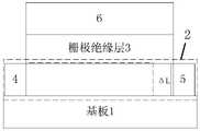
图1为本发明实施例中一种驱动薄膜晶体管的结构原理图FIG. 1 is a schematic structural diagram of a driving thin film transistor according to an embodiment of the present invention
图2为本发明实施例中驱动薄膜晶体管Ids相对变化率的示意图;FIG. 2 is a schematic diagram of the relative change rate of the driving thin film transistor Ids in an embodiment of the present invention;
图3为本发明示出了驱动薄膜晶体管饱和区斜率的示意图。FIG. 3 is a schematic diagram illustrating the slope of the saturation region of the driving thin film transistor according to the present invention.
附图标记:Reference number:
1-基板;2-有源层;3-栅极绝缘层;4-源区;5-漏区;6-栅极。1-substrate; 2-active layer; 3-gate insulating layer; 4-source region; 5-drain region; 6-gate.
具体实施方式Detailed ways
正如背景技术中所述,OLED显示器件在长时间点亮后,器件的性能会发生退化,OLED显示器件的开启电压降上升,即OLED显示器件两端的电压上升,导致驱动薄膜晶体管源漏两端的电压减小,经过OLED显示器件的电流随之减小,OLED显示器件的亮度降低,寿命减小。发明人研究发现,出现这种问题的原因在于OLED显示器件在点亮阶段,驱动薄膜晶体管工作在饱和区,此时,驱动薄膜晶体管存在一定饱和区斜率,在OLED 显示器件在长时间点亮后,器件的性能会发生退化,驱动薄膜晶体管的饱和区斜率增大,而驱动薄膜晶体管的饱和区斜率增大会进一步导致经过 OLED显示器件的电流减小,OLED显示器件的亮度降低,寿命减小。As mentioned in the Background Art, after the OLED display device is lit for a long time, the performance of the device will be degraded, and the turn-on voltage drop of the OLED display device will increase, that is, the voltage across the OLED display device will increase, resulting in the driving thin film transistor. When the voltage decreases, the current passing through the OLED display device decreases accordingly, the brightness of the OLED display device decreases, and the life span of the OLED display device decreases. The inventor found that the reason for this problem is that the driving thin film transistor works in the saturation region during the lighting stage of the OLED display device. At this time, the driving thin film transistor has a certain saturation region slope. After the OLED display device is lit for a long time, the , the performance of the device will be degraded, the slope of the saturation region of the driving thin film transistor will increase, and the increase in the slope of the saturation region of the driving thin film transistor will further reduce the current passing through the OLED display device, the brightness of the OLED display device, and the life.
为使本发明实施例的目的、技术方案和优点更加清楚,下面将结合附图对本发明的技术方案进行清楚、完整地描述,显然,所描述的实施例是本发明一部分实施例,而不是全部的实施例。基于本发明中的实施例,本领域普通技术人员在没有做出创造性劳动前提下所获得的所有其他实施例,都属于本发明保护的范围。In order to make the purposes, technical solutions and advantages of the embodiments of the present invention clearer, the technical solutions of the present invention will be clearly and completely described below with reference to the accompanying drawings. Obviously, the described embodiments are part of the embodiments of the present invention, but not all of them. example. Based on the embodiments of the present invention, all other embodiments obtained by those of ordinary skill in the art without creative efforts shall fall within the protection scope of the present invention.
本发明实施例提供一种驱动薄膜晶体管,如图1所示,至少包括:基板1、有源层2、栅极绝缘层3,所述有源层包括源区、漏区及沟道;其中沟道长度处于35μm至50μm区间范围内,优选地,沟道长度L为37μm、 40μm、42和45.8μm中任一点或选自任意两点组成的区域范围;沟道宽度 w为3μm至3.5μm。优选沟道宽度W与长度L的比值为0.06-0.1。An embodiment of the present invention provides a driving thin film transistor, as shown in FIG. 1, which at least includes: a
本发明实施例中驱动薄膜晶体管具有沟道长度调制效应,如公式(1) 所示,In the embodiment of the present invention, the driving thin film transistor has a channel length modulation effect, as shown in formula (1),

其中,Ids表示源漏电流,即流经OLED显示器件的电流,μ表示载流子的迁移率,Cox表示单位面积的栅氧化电容,
由公式(1)可以看出,当增加沟道长度时,源漏电流增大,即流经 OLED显示器件的电流增大,弱化了器件本身的沟道长度调制效应,有助于改善饱和区斜率,使驱动薄膜晶体管保持稳定的驱动能力,器件经过长时间点亮后,驱动薄膜晶体管源漏两端的电压变化幅度减小,减缓了OLED 显示器件的电流速率,使得OLED显示器件更长时间的处于较高的亮度状态,改善OLED器件寿命。It can be seen from formula (1) that when the channel length is increased, the source-drain current increases, that is, the current flowing through the OLED display device increases, which weakens the channel length modulation effect of the device itself and helps to improve the saturation region. The slope of the driving thin film transistor keeps the driving ability stable. After the device is lit for a long time, the voltage change across the source and drain of the driving thin film transistor decreases, which slows down the current rate of the OLED display device and makes the OLED display device last longer. In a higher brightness state, improving the life of the OLED device.
本发明实施例中,制备35μm至50μm区间范围内的沟道长度时,可以按照以下的工艺进行,按阵列的正常工艺使非晶硅经过晶化形成多晶硅,然后在后续黄光、多晶硅刻蚀工艺段新增一张Mask,使刻蚀沟道长度增加ΔL,然后继续栅极绝缘层3成膜、栅极6工艺。这仅仅给出了实现制备35μm 至50μm区间范围内的沟道长度的一种方式,在实际应用中,还可以通过其他的方式制备,本发明并不以此为限。In the embodiment of the present invention, when preparing the channel length in the range of 35 μm to 50 μm, the following process can be performed. According to the normal process of the array, the amorphous silicon is crystallized to form polysilicon, and then the subsequent yellow light and polysilicon are etched. A new mask is added to the process section to increase the length of the etched channel by ΔL, and then the gate insulating layer 3 film formation and
由于OLED显示器件在长时间点亮后,器件的性能会发生退化,OLED 显示器件的开启电压降上升,即OLED显示器件两端的电压上升,导致驱动薄膜晶体管源漏两端的电压减小,经过OLED显示器件的电流随之减小, OLED显示器件的亮度降低,寿命减小,现有的OLED显示器件长时间使用后,源漏电流变化率为0.29%左右。Since the performance of the OLED display device will degrade after being lit for a long time, the turn-on voltage drop of the OLED display device will increase, that is, the voltage across the OLED display device will increase, resulting in a decrease in the voltage across the source and drain of the driving thin film transistor. The current of the display device decreases accordingly, the brightness of the OLED display device decreases, and the lifespan of the OLED display device decreases. After the existing OLED display device is used for a long time, the source-drain current change rate is about 0.29%.
本发明实施例中,当沟道长度处于35μm至50μm区间范围内时,饱和区的电流Ids的相对变化率由现有的0.29%可以降低至0.15%,使得驱动薄膜晶体管饱和区的斜率降低,驱动薄膜晶体管的驱动能力增强,,器件经过长时间点亮后,驱动薄膜晶体管源漏两端的电压变化幅度减小,减缓了OLED 显示器件的电流速率,使得OLED显示器件更长时间的处于较高的亮度状态,改善了OLED显示器件的寿命。In the embodiment of the present invention, when the channel length is in the range of 35 μm to 50 μm, the relative change rate of the current Ids in the saturation region can be reduced from the existing 0.29% to 0.15%, so that the slope of the saturation region of the driving thin film transistor is reduced , the driving ability of the driving thin film transistor is enhanced, and after the device is lit for a long time, the voltage change across the source and drain of the driving thin film transistor decreases, which slows down the current rate of the OLED display device and makes the OLED display device stay in a longer period of time. The high brightness state improves the lifetime of the OLED display device.
为了进一步降低驱动薄膜晶体管饱和区的电流的斜率,还可以通过改变制作驱动薄膜晶体管的工艺条件实现具体的可以从以下几点进行改变,该改变栅极绝缘层的厚度、改变栅极绝缘层的结构、改变有源层区厚度、改变源区/漏区的注入计量和能量、改变源区和漏区退火时间,改变有源层的氢化时间,上述多个条件并非是严格意义上的工艺条件的改变,其中前三种改变实际是通过工艺条件的改变对驱动薄膜晶体管的结构进行的改变,为方便描述,在本实施例中将上述六种改变统称为工艺条件改变。In order to further reduce the slope of the current in the saturation region of the driving thin film transistor, the process conditions for manufacturing the driving thin film transistor can also be changed. The specific changes can be made from the following points: changing the thickness of the gate insulating layer, changing the Structure, change the thickness of the active layer, change the implantation metering and energy of the source/drain region, change the annealing time of the source and drain regions, change the hydrogenation time of the active layer, the above conditions are not strictly process conditions The first three changes are actually changes to the structure of the driving thin film transistor through changes in process conditions. For convenience of description, the above six changes are collectively referred to as changes in process conditions in this embodiment.
具体的,驱动薄膜晶体管中的栅极绝缘层的厚度设置为大于或等于 80nm,小于或等于120nm,优选地厚度为90nm,100nm,110nm。Specifically, the thickness of the gate insulating layer in the driving thin film transistor is set to be greater than or equal to 80 nm and less than or equal to 120 nm, and preferably the thickness is 90 nm, 100 nm, or 110 nm.
本发明实施例中,栅极绝缘层的厚度大于或等于80nm,小于或等于 120nm,这一厚度相对现有的驱动薄膜晶体管中栅极绝缘层的厚度相对减薄,而当栅极绝缘层减薄之后,栅极和沟道的距离减小,能够增加栅极对沟道的控制能力,降低曲线的亚阈值摆幅(S.S),改善沟道及界面质量,可以在沟道长度相较现有技术中沟道长度增加的前提下,使得驱动薄膜晶体管饱和区的电流斜率进一步降低,进一步增强驱动薄膜晶体管的驱动能力,使得OLED显示器件更长时间的处于较高的亮度状态,改善OLED显示器件的寿命。当然,单独采用本实施例描述的将栅极绝缘层的厚度大于或等于 80nm,小于或等于120nm的范围内也是可以使得驱动薄膜晶体管饱和区的电流斜率降低,增强驱动薄膜晶体管的驱动能力,增加OLED器件的使用寿命的。In the embodiment of the present invention, the thickness of the gate insulating layer is greater than or equal to 80 nm and less than or equal to 120 nm, which is relatively thinner than the thickness of the gate insulating layer in the existing driving thin film transistor, and when the gate insulating layer is reduced After thinning, the distance between the gate and the channel is reduced, which can increase the control ability of the gate to the channel, reduce the sub-threshold swing (S.S) of the curve, and improve the channel and interface quality. Under the premise of increasing the channel length in the prior art, the current slope in the saturation region of the driving thin film transistor is further reduced, and the driving capability of the driving thin film transistor is further enhanced, so that the OLED display device is in a higher brightness state for a longer time, and the OLED display is improved. device lifetime. Of course, if the thickness of the gate insulating layer is greater than or equal to 80 nm and less than or equal to 120 nm as described in this embodiment alone, the current slope of the saturation region of the driving thin film transistor can be reduced, the driving ability of the driving thin film transistor can be enhanced, and the driving ability of the driving thin film transistor can be increased. the service life of OLED devices.
为了进一步降低驱动薄膜晶体管饱和区的电流的斜率,可以改变栅极绝缘层的结构,在本实施例中沉积栅极绝缘层时可以将栅极绝缘层设置为双层结构,其中,先沉积一层氧化硅,在氧化硅上再沉积一层氮化硅。In order to further reduce the slope of the current in the saturation region of the driving thin film transistor, the structure of the gate insulating layer can be changed. A layer of silicon oxide is deposited, and a layer of silicon nitride is deposited on the silicon oxide.
本发明实施例中,栅极绝缘层使用双层结构,相比于现有的栅极绝缘层使用单层结构,能够增加栅极对沟道的控制能力,具体的,该双层结构的栅极绝缘层可以包括层叠的氧化硅和氮化硅同时相对现有的单层结构的栅极绝缘层的总厚度不变,能够增加栅极对沟道的控制能力,有利于降低曲线的亚阈值摆幅(S.S),使得驱动薄膜晶体管饱和区的斜率降低,驱动薄膜晶体管的驱动能力增强,器件经过长时间点亮后,驱动薄膜晶体管源漏两端的电压变化幅度减小,减缓了OLED显示器件的电流速率,使得OLED 显示器件更长时间的处于较高的亮度状态,改善了OLED显示器件的寿命。In the embodiment of the present invention, the gate insulating layer uses a double-layer structure. Compared with the existing gate insulating layer using a single-layer structure, the control ability of the gate to the channel can be increased. Specifically, the gate of the double-layer structure can be The polar insulating layer can include stacked silicon oxide and silicon nitride, while the total thickness of the gate insulating layer of the existing single-layer structure is unchanged, which can increase the control ability of the gate to the channel and is beneficial to reduce the sub-threshold value of the curve. The swing (S.S) reduces the slope of the saturation region of the driving thin film transistor and enhances the driving ability of the driving thin film transistor. After the device is lit for a long time, the voltage change across the source and drain of the driving thin film transistor decreases, which slows down the OLED display device. The high current rate enables the OLED display device to be in a higher brightness state for a longer period of time, thereby improving the lifespan of the OLED display device.
如图1所示,驱动薄膜晶体管包括源区4、漏区5,栅极绝缘层3,栅极6,具体的,以PMOS为例进行说明,当VDS增大时,耗尽区内电场强度随之增强,沟道中电子数增多,这一过程相当于漏区与沟道存在耦合电容,减弱了栅极对沟道的控制能力,因此,为进一步降低驱动薄膜晶体管饱和区的电流的斜率,在可选的实施例中,采用硼离子进行注入,可以改变源区4/漏区5的注入计量和能量,源区4/漏区5的注入剂量大于或等于 5×10¹⁴个/cm2小于或等于1×1015个/cm2,源区/漏区的注入能量大于或等于25KeV小于或等于35KeV。该实施例相对现有的源区/漏区的注入剂量和注入能量减小了75%-90%,源区/漏区的注入剂量和注入能量的减小,使得耗尽区电荷的数量和分布减小,减小了寄生电容,可以增加栅极对沟道的控制能力,降低曲线的亚阈值摆幅(S.S),改善沟道及界面质量,使得驱动薄膜晶体管饱和区的斜率降低,驱动薄膜晶体管的驱动能力增强,改善了 OLED显示器件的寿命。As shown in FIG. 1, the driving thin film transistor includes a
在本实施例中,减小漏区与沟道的寄生电容还可以通过减薄有源层的厚度实现,具体的在本实施例中可以通过将有源层的厚度控制在大于60nm 小于80nm范围内,优选地,厚度为70nm。有源层厚度减薄相当于减小了漏极与沟道的寄生电容,可以增加栅极对有源层沟道的控制能力,降低曲线的亚阈值摆幅(S.S),改善沟道及界面质量,使得驱动薄膜晶体管饱和区的斜率降低,驱动薄膜晶体管的驱动能力增强,改善了OLED显示器件的寿命。In this embodiment, reducing the parasitic capacitance between the drain region and the channel can also be achieved by reducing the thickness of the active layer. Specifically, in this embodiment, the thickness of the active layer can be controlled in the range of greater than 60 nm and less than 80 nm. Inside, preferably, the thickness is 70 nm. The thinning of the active layer thickness is equivalent to reducing the parasitic capacitance between the drain and the channel, which can increase the gate’s ability to control the active layer channel, reduce the sub-threshold swing (S.S) of the curve, and improve the channel and interface. Therefore, the slope of the saturation region of the driving thin film transistor is reduced, the driving capability of the driving thin film transistor is enhanced, and the lifespan of the OLED display device is improved.
为进一步降低驱动薄膜晶体管饱和区的电流的斜率,在另一可选的实施例中,驱动薄膜晶体管的退火时间可以控制在大于或等于45分钟小于或等于90分钟,优选地,退火时间为60分钟,70分钟。In order to further reduce the slope of the current in the saturation region of the driving thin film transistor, in another optional embodiment, the annealing time of the driving thin film transistor can be controlled to be greater than or equal to 45 minutes and less than or equal to 90 minutes, preferably, the annealing time is 60 minutes. minutes, 70 minutes.
本发明实施例中,驱动薄膜晶体管的退火时间控制在大于或等于45分钟小于或等于90分钟,相对现有的驱动薄膜晶体管的退火时间小于45分钟有所增加,可以降低源区和漏区中杂质的浓度,增加栅极对沟道的控制能力,降低曲线的亚阈值摆幅(S.S),改善沟道及界面质量,使得驱动薄膜晶体管饱和区的斜率降低,增强驱动薄膜晶体管的驱动能力,改善OLED 显示器件的寿命。In the embodiment of the present invention, the annealing time of the driving thin film transistor is controlled to be greater than or equal to 45 minutes and less than or equal to 90 minutes, which is increased compared to the annealing time of the existing driving thin film transistor of less than 45 minutes, which can reduce the time in the source region and the drain region. The concentration of impurities increases the control ability of the gate to the channel, reduces the sub-threshold swing (S.S) of the curve, improves the channel and interface quality, reduces the slope of the saturation region of the driving thin film transistor, and enhances the driving ability of the driving thin film transistor. Improve the lifespan of OLED display devices.
为进一步降低驱动薄膜晶体管饱和区的电流的斜率,可以通过减小有源层的缺陷实现,具体的,在可选的实施例中,有源层氢化时间大于或等于45分钟小于或等于90分钟,优选地,氢化时间为60分钟,70分钟。In order to further reduce the slope of the current driving the saturation region of the thin film transistor, it can be achieved by reducing the defects of the active layer. Specifically, in an optional embodiment, the hydrogenation time of the active layer is greater than or equal to 45 minutes and less than or equal to 90 minutes. , preferably, the hydrogenation time is 60 minutes, 70 minutes.
在本发明实施例中,有源层氢化时间大于或等于45分钟小于或等于90 分钟相对现有技术中的氢化时间小于45分钟有所增加,而氢化时间的增加减小了有源层的缺陷,可以改善有源层中沟道和栅极绝缘层的界面质量,使得驱动薄膜晶体管饱和区的斜率降低,增强驱动薄膜晶体管的驱动能力,改善OLED显示器件的寿命。In the embodiment of the present invention, the hydrogenation time of the active layer is greater than or equal to 45 minutes and less than or equal to 90 minutes, which is increased compared to the hydrogenation time of less than 45 minutes in the prior art, and the increase of the hydrogenation time reduces the defects of the active layer , the interface quality of the channel and the gate insulating layer in the active layer can be improved, the slope of the saturation region of the driving thin film transistor can be reduced, the driving ability of the driving thin film transistor can be enhanced, and the life of the OLED display device can be improved.
本发明实施例中提出的增加沟道的长度或者变更驱动薄膜晶体管的制备条件,可以将采用上述实施例中至少之一的条件制备驱动薄膜晶体管。To increase the length of the channel or to change the fabrication conditions of the driving thin film transistor proposed in the embodiments of the present invention, the driving thin film transistor may be fabricated by adopting at least one of the conditions in the above-mentioned embodiments.
本发明实施例中提出的增加沟道的长度或者变更驱动薄膜晶体管的制备条件等对于源漏电流的增大或者驱动薄膜晶体管饱和区斜率的减小都具有积极的影响,对源漏电流影响如表1所示,对驱动薄膜晶体管饱和区斜率的影响如表2所示。Increasing the length of the channel or changing the preparation conditions of the driving thin film transistor proposed in the embodiment of the present invention has a positive influence on the increase of the source-drain current or the reduction of the slope of the saturation region of the driving thin-film transistor, and the influence on the source-drain current such as As shown in Table 1, the influence on the slope of the saturation region of the driving thin film transistor is shown in Table 2.
表1Table 1
对应的图2示出了通过沟道长度改变和工艺条件与现有技术(Baseline) 的改变对应的Ids的相对变化率对比的示意图。Corresponding Figure 2 shows a schematic diagram comparing the relative rate of change of Ids by channel length change and process condition change corresponding to the prior art (Baseline).
表2Table 2

对应的图3示出了通过工艺条件的改变,即上述表2中任意至少之一项改变后与现有技术(Baseline)饱和区斜率的对比示意图。Correspondingly, FIG. 3 shows a schematic diagram comparing the slope of the saturation region with the prior art (Baseline) after changing at least one of the above-mentioned Table 2 by changing the process conditions.
由于OLED显示器件在长时间点亮后,器件的性能会发生退化,OLED 显示器件的开启电压降上升,即OLED显示器件两端的电压上升,导致驱动薄膜晶体管源漏两端的电压减小,经过OLED显示器件的电流随之减小,源漏电流减小,驱动薄膜晶体管的饱和区斜率增大,因此减小源漏电流的相对变化率或者减小驱动薄膜晶体管的饱和区斜率的相对变化率都可以延长OLED显示器件的寿命。Since the performance of the OLED display device will degrade after being lit for a long time, the turn-on voltage drop of the OLED display device will increase, that is, the voltage across the OLED display device will increase, resulting in a decrease in the voltage across the source and drain of the driving thin film transistor. The current of the display device decreases, the source-drain current decreases, and the slope of the saturation region of the driving thin-film transistor increases, so reducing the relative rate of change of the source-drain current or reducing the relative rate of change of the saturation region slope of the driving thin-film transistor are both The lifetime of the OLED display device can be extended.
如表1所示,当有源层中沟道长度处于35μm至50μm区间范围内时Ids的相对变化率小于或等于0.15%;当栅极绝缘层的厚度大于或等于80nm,小于或等于120nm,且源极/漏极的注入剂量大于5×1014个/cm2小于 1×10¹⁵个/cm2,源极/漏极的注入能量大于25KeV小于35KeV且驱动薄膜晶体管在离子注入后的退火时间大于45分钟小于90分钟时Ids的相对变化率小于或等于0.20%,这两个相对变化率与现有驱动薄膜晶体管的0.29%相比都减小,改善了OLED显示器件的寿命。As shown in Table 1, when the channel length in the active layer is in the range of 35 μm to 50 μm, the relative change rate of Ids is less than or equal to 0.15%; when the thickness of the gate insulating layer is greater than or equal to 80 nm, less than or equal to 120 nm , and the implant dose of source/drain is greater than 5×10¹⁴ /cm2 and less than 1×10¹⁵ /cm2 , the implant energy of source/drain is greater than 25KeV and less than 35KeV, and the driving thin film transistor after ion implantation When the annealing time is greater than 45 minutes and less than 90 minutes, the relative change rate of Ids is less than or equal to 0.20%, both of which are reduced compared with 0.29% of the existing driving thin film transistor, which improves the lifetime of the OLED display device.
如表2所示,当驱动薄膜晶体管栅极绝缘层的厚度大于或等于80nm,小于或等于120nm,且源极/漏极的注入剂量大于或等于5×1014个/cm2小于或等于1×1015个/cm2,源极/漏极的注入能量大于或等于25KeV小于或等于35KeV时饱和区斜率相对变化率为不大于0.132%;当驱动薄膜晶体管源极/漏极的注入剂量大于5×1014个/cm2小于1×1015个/cm2,源极/漏极的注入能量大于或等于25KeV小于或等于35KeV时饱和区斜率相对变化率为小于或等于0.137%;当栅极绝缘层包括双层结构氧化硅和氮化硅时饱和区斜率相对变化率为小于或等于0.128%,;当有源层氢化时间大于45分钟小于90分钟时饱和区斜率相对变化率小于或等于0.143%;当有源层的厚度大于60nm小于80nm时饱和区斜率相对变化率小于或等于0.146%,这几个相对变化率与现有驱动薄膜晶体管的0.148%相比都减小,改善了OLED显示器件的寿命。As shown in Table 2, when the thickness of the gate insulating layer of the driving thin film transistor is greater than or equal to 80 nm, less than or equal to 120 nm, and the implantation dose of the source/drain is greater than or equal to 5×10¹⁴ /cm2 is less than or equal to 1 ×10¹⁵ pcs/cm2 , when the source/drain implant energy is greater than or equal to 25KeV and less than or equal to 35KeV, the relative change rate of the slope of the saturation region is not greater than 0.132%; when the source/drain implant dose of the driving thin film transistor is greater than 5×10¹⁴ /cm2 is less than 1×10¹⁵ /cm2 , the source/drain injection energy is greater than or equal to 25KeV and less than or equal to 35KeV, the relative change rate of the slope of the saturation region is less than or equal to 0.137%; When the polar insulating layer includes double-layer structure silicon oxide and silicon nitride, the relative change rate of the saturation region slope is less than or equal to 0.128%; when the hydrogenation time of the active layer is greater than 45 minutes and less than 90 minutes, the relative change rate of the saturation region slope is less than or equal to 0.143%; when the thickness of the active layer is greater than 60 nm and less than 80 nm, the relative change rate of the slope of the saturation region is less than or equal to 0.146%, and these relative change rates are all reduced compared with 0.148% of the existing driving thin film transistor, which improves the OLED Displays the lifetime of the device.
本发明施例提供一种阵列基板,阵列基板上分散有若干个驱动薄膜晶体管,其中对应于蓝色像素和绿色像素的驱动薄膜晶体管采用上述驱动薄膜晶体管。An embodiment of the present invention provides an array substrate, on which a plurality of driving thin film transistors are dispersed, wherein the driving thin film transistors corresponding to blue pixels and green pixels are the above driving thin film transistors.
对应于蓝色像素的驱动薄膜晶体管中沟道的长度L1,对应于绿色像素的驱动薄膜晶体管中沟道的长度L2,对应于红色像素的驱动薄膜晶体管中沟道的长度L3,其中L1和L2大于L3;优选L1与L3的差值大于等于10μm,优选L2与L3的差值大于等于10μm,L3为18-35μm。Corresponding to the length L1 of the channel in the driving thin film transistor of the blue pixel, corresponding to the length L2 of the channel in the driving thin film transistor of the green pixel, corresponding to the length L3 of the channel in the driving thin film transistor of the red pixel, wherein L1 and L2 Greater than L3; preferably, the difference between L1 and L3 is greater than or equal to 10 μm, preferably the difference between L2 and L3 is greater than or equal to 10 μm, and L3 is 18-35 μm.
本发明实施例中的阵列基板,使用上述驱动薄膜晶体管,通过增加沟道长度,弱化器件本身的沟道长度调制效应,使得驱动薄膜晶体管饱和区的斜率降低,驱动薄膜晶体管的驱动能力增强,改善了OLED显示器件的寿命;或者通过增加栅极的控制能力,降低曲线的亚阈值摆幅(S.S),改善沟道及界面质量,使得驱动薄膜晶体管饱和区的斜率降低,驱动薄膜晶体管的驱动能力增强,改善了OLED显示器件的寿命。The array substrate in the embodiment of the present invention uses the above-mentioned driving thin film transistor, and by increasing the channel length, the channel length modulation effect of the device itself is weakened, so that the slope of the saturation region of the driving thin film transistor is reduced, the driving ability of the driving thin film transistor is enhanced, and the The life of the OLED display device is improved; or by increasing the control ability of the gate, reducing the sub-threshold swing (S.S) of the curve, improving the channel and interface quality, reducing the slope of the saturation region of the driving thin film transistor, and the driving ability of the driving thin film transistor. Enhanced, improving the lifespan of OLED display devices.
本发明实施例提供一种显示器件,包括上述阵列基板。An embodiment of the present invention provides a display device including the above-mentioned array substrate.
本发明实施例中的显示器件使用上述阵列基板,通过增加沟道长度,弱化器件本身的沟道长度调制效应,使得驱动薄膜晶体管饱和区的斜率降低,驱动薄膜晶体管的驱动能力增强,改善了OLED显示器件的寿命;或者通过增加栅极的控制能力,降低曲线的亚阈值摆幅(S.S),改善沟道及界面质量,使得驱动薄膜晶体管饱和区的斜率降低,驱动薄膜晶体管的驱动能力增强,改善了OLED显示器件的寿命。The display device in the embodiment of the present invention uses the above-mentioned array substrate. By increasing the channel length, the channel length modulation effect of the device itself is weakened, so that the slope of the saturation region of the driving thin film transistor is reduced, the driving ability of the driving thin film transistor is enhanced, and the OLED is improved. The life of the display device; or by increasing the control ability of the gate, reducing the sub-threshold swing (S.S) of the curve, improving the channel and interface quality, reducing the slope of the saturation region of the driving thin film transistor, and enhancing the driving ability of the driving thin film transistor, The lifetime of the OLED display device is improved.
显然,上述实施例仅仅是为清楚地说明所作的举例,而并非对实施方式的限定。对于所属领域的普通技术人员来说,在上述说明的基础上还可以做出其它不同形式的变化或变动。这里无需也无法对所有的实施方式予以穷举。而由此所引伸出的显而易见的变化或变动仍处于本发明创造的保护范围之中。Obviously, the above-mentioned embodiments are only examples for clear description, and are not intended to limit the implementation manner. For those of ordinary skill in the art, changes or modifications in other different forms can also be made on the basis of the above description. There is no need and cannot be exhaustive of all implementations here. And the obvious changes or changes derived from this are still within the protection scope of the present invention.
Claims (10)
Translated fromChinesePriority Applications (1)
| Application Number | Priority Date | Filing Date | Title |
|---|---|---|---|
| CN201811095887.1ACN109449210B (en) | 2018-09-19 | 2018-09-19 | Array substrate and display device |
Applications Claiming Priority (1)
| Application Number | Priority Date | Filing Date | Title |
|---|---|---|---|
| CN201811095887.1ACN109449210B (en) | 2018-09-19 | 2018-09-19 | Array substrate and display device |
Publications (2)
| Publication Number | Publication Date |
|---|---|
| CN109449210A CN109449210A (en) | 2019-03-08 |
| CN109449210Btrue CN109449210B (en) | 2022-06-10 |
Family
ID=65530722
Family Applications (1)
| Application Number | Title | Priority Date | Filing Date |
|---|---|---|---|
| CN201811095887.1AActiveCN109449210B (en) | 2018-09-19 | 2018-09-19 | Array substrate and display device |
Country Status (1)
| Country | Link |
|---|---|
| CN (1) | CN109449210B (en) |
Families Citing this family (2)
| Publication number | Priority date | Publication date | Assignee | Title |
|---|---|---|---|---|
| CN110797413A (en)* | 2019-11-11 | 2020-02-14 | 云谷(固安)科技有限公司 | Thin film transistor, pixel driving circuit and display panel |
| CN112086467B (en)* | 2020-09-02 | 2023-03-24 | 武汉华星光电半导体显示技术有限公司 | Display panel |
Citations (9)
| Publication number | Priority date | Publication date | Assignee | Title |
|---|---|---|---|---|
| CN1914552A (en)* | 2004-01-26 | 2007-02-14 | 株式会社半导体能源研究所 | Electric appliance, semiconductor device and manufacturing method thereof |
| CN101063782A (en)* | 2006-04-28 | 2007-10-31 | Lg.菲利浦Lcd株式会社 | Liquid crystal display device and array substrate for the same |
| CN101236992A (en)* | 2006-12-12 | 2008-08-06 | 三菱电机株式会社 | Thin film transistor and manufacturing method thereof |
| JP2010049056A (en)* | 2008-08-22 | 2010-03-04 | Canon Inc | Organic el display |
| CN102709184A (en)* | 2011-05-13 | 2012-10-03 | 京东方科技集团股份有限公司 | Polysilicon active layer-containing thin film transistor, manufacturing method thereof and array substrate |
| CN205561900U (en)* | 2016-03-16 | 2016-09-07 | 黑龙江大学 | Power / magnetism multi -functional sensor |
| CN206471332U (en)* | 2016-12-26 | 2017-09-05 | 云谷(固安)科技有限公司 | Display panel and display device |
| CN107706243A (en)* | 2017-09-20 | 2018-02-16 | 武汉华星光电半导体显示技术有限公司 | Low-temperature polysilicon film transistor and preparation method thereof and array base palte |
| CN107887418A (en)* | 2017-10-19 | 2018-04-06 | 武汉天马微电子有限公司 | Display panel and display device |
Family Cites Families (7)
| Publication number | Priority date | Publication date | Assignee | Title |
|---|---|---|---|---|
| JP4265552B2 (en)* | 1993-02-10 | 2009-05-20 | セイコーエプソン株式会社 | Thin film transistor and manufacturing method thereof |
| WO1995003629A1 (en)* | 1993-07-26 | 1995-02-02 | Seiko Epson Corporation | Thin film semiconductor device, its manufacture, and display system |
| US7612749B2 (en)* | 2003-03-04 | 2009-11-03 | Chi Mei Optoelectronics Corporation | Driving circuits for displays |
| EP2183780A4 (en)* | 2007-08-02 | 2010-07-28 | Applied Materials Inc | THIN FILM TRANSISTORS USING THIN FILM SEMICONDUCTOR MATERIALS |
| CN105206626B (en)* | 2015-11-09 | 2018-11-20 | 深圳市华星光电技术有限公司 | Array substrate and preparation method thereof, display device |
| CN105428240A (en)* | 2015-12-16 | 2016-03-23 | 信利(惠州)智能显示有限公司 | Thin-film transistor and preparation method thereof |
| CN107204376B (en)* | 2017-05-26 | 2019-12-27 | 厦门天马微电子有限公司 | Thin film transistor, manufacturing method thereof, array substrate and display device |
- 2018
- 2018-09-19CNCN201811095887.1Apatent/CN109449210B/enactiveActive
Patent Citations (9)
| Publication number | Priority date | Publication date | Assignee | Title |
|---|---|---|---|---|
| CN1914552A (en)* | 2004-01-26 | 2007-02-14 | 株式会社半导体能源研究所 | Electric appliance, semiconductor device and manufacturing method thereof |
| CN101063782A (en)* | 2006-04-28 | 2007-10-31 | Lg.菲利浦Lcd株式会社 | Liquid crystal display device and array substrate for the same |
| CN101236992A (en)* | 2006-12-12 | 2008-08-06 | 三菱电机株式会社 | Thin film transistor and manufacturing method thereof |
| JP2010049056A (en)* | 2008-08-22 | 2010-03-04 | Canon Inc | Organic el display |
| CN102709184A (en)* | 2011-05-13 | 2012-10-03 | 京东方科技集团股份有限公司 | Polysilicon active layer-containing thin film transistor, manufacturing method thereof and array substrate |
| CN205561900U (en)* | 2016-03-16 | 2016-09-07 | 黑龙江大学 | Power / magnetism multi -functional sensor |
| CN206471332U (en)* | 2016-12-26 | 2017-09-05 | 云谷(固安)科技有限公司 | Display panel and display device |
| CN107706243A (en)* | 2017-09-20 | 2018-02-16 | 武汉华星光电半导体显示技术有限公司 | Low-temperature polysilicon film transistor and preparation method thereof and array base palte |
| CN107887418A (en)* | 2017-10-19 | 2018-04-06 | 武汉天马微电子有限公司 | Display panel and display device |
Non-Patent Citations (4)
| Title |
|---|
| Stability Enhancement of Polysilicon Thin-Film Transistors Using Stacked Plasma-Enhanced Chemical Vapor Deposited SiO2/SiNx Gate Dielectric;Byoung-Deog CHOI等;《Japanese Journal of Applied Physics》;20050930;第44卷(第9A期);第6417页以及图1* |
| 实现多晶硅薄膜等离子氢化的新工艺;曾祥斌等;《光电子技术》;20000930;第20卷(第3期);179-182页,图1* |
| 高品质低温多晶硅薄膜晶体管的制作与周边一体化设计;黄金英;《中国优秀博士学位论文全文数据库》;20070415(第4期);论文58页、65-68页、74页,表4.2,图4.9,图4.22* |
| 黄金英.高品质低温多晶硅薄膜晶体管的制作与周边一体化设计.《中国优秀博士学位论文全文数据库》.2007,(第4期),I135-17.* |
Also Published As
| Publication number | Publication date |
|---|---|
| CN109449210A (en) | 2019-03-08 |
Similar Documents
| Publication | Publication Date | Title |
|---|---|---|
| US9373724B2 (en) | Method of driving transistor and device including transistor driven by the method | |
| CN101626036B (en) | Thin-film transistor and manufacture method thereof and comprise the panel display apparatus of this transistor | |
| CN101794809B (en) | Organic light emitting display device and method of manufacturing the same | |
| CN109817645B (en) | Array substrate and manufacturing method thereof, display panel, electronic device | |
| CN105390551B (en) | Thin film transistor (TFT) and its manufacturing method, array substrate, display device | |
| US20110012125A1 (en) | Thin film transistor and active matrix display | |
| JP5285024B2 (en) | Thin film transistor and organic light emitting display device having the same | |
| CN106486499B (en) | A circuit structure and manufacturing method and display panel | |
| CN103762174A (en) | Preparation method for thin-film transistor | |
| JP6872133B2 (en) | Display devices and electronic devices | |
| CN104538458A (en) | Display device, array substrate, thin film transistor and fabricating method thereof | |
| CN110752219B (en) | A thin film transistor and display panel | |
| CN104347813B (en) | Transistor, the method for manufacturing transistor and the electronic device including transistor | |
| CN109560044A (en) | A method of inhibiting thin film transistor (TFT) threshold voltage shift | |
| CN105161516A (en) | Organic light emitting display and manufacture method thereof | |
| TWI621270B (en) | Thin film transistor element and thin film transistor display device | |
| CN109449210B (en) | Array substrate and display device | |
| US9768324B2 (en) | Co-planar oxide semiconductor TFT substrate structure and manufacture method thereof | |
| WO2017181449A1 (en) | Thin film transistor, manufacturing method for thin film transistor, and cmos device | |
| CN103367456B (en) | Thin-film transistor and manufacture method thereof | |
| US20070051956A1 (en) | Thin film transistor | |
| CN104332501B (en) | NLDMOS device and its manufacture method | |
| CN114628529A (en) | Driving backboard, manufacturing method thereof and display panel | |
| CN103762169A (en) | Bottom gate thin film transistor and manufacturing method thereof | |
| GB2460395A (en) | Thin film transistor and active matrix display |
Legal Events
| Date | Code | Title | Description |
|---|---|---|---|
| PB01 | Publication | ||
| PB01 | Publication | ||
| SE01 | Entry into force of request for substantive examination | ||
| SE01 | Entry into force of request for substantive examination | ||
| GR01 | Patent grant | ||
| GR01 | Patent grant |