CN109427382B - Memory cell and memory cell array - Google Patents
Memory cell and memory cell arrayDownload PDFInfo
- Publication number
- CN109427382B CN109427382BCN201810954519.1ACN201810954519ACN109427382BCN 109427382 BCN109427382 BCN 109427382BCN 201810954519 ACN201810954519 ACN 201810954519ACN 109427382 BCN109427382 BCN 109427382B
- Authority
- CN
- China
- Prior art keywords
- memory cell
- transistors
- capacitor
- memory cells
- ferroelectric
- Prior art date
- Legal status (The legal status is an assumption and is not a legal conclusion. Google has not performed a legal analysis and makes no representation as to the accuracy of the status listed.)
- Active
Links
Images


Classifications
- G—PHYSICS
- G11—INFORMATION STORAGE
- G11C—STATIC STORES
- G11C11/00—Digital stores characterised by the use of particular electric or magnetic storage elements; Storage elements therefor
- G11C11/21—Digital stores characterised by the use of particular electric or magnetic storage elements; Storage elements therefor using electric elements
- G11C11/22—Digital stores characterised by the use of particular electric or magnetic storage elements; Storage elements therefor using electric elements using ferroelectric elements
- G11C11/221—Digital stores characterised by the use of particular electric or magnetic storage elements; Storage elements therefor using electric elements using ferroelectric elements using ferroelectric capacitors
- G—PHYSICS
- G11—INFORMATION STORAGE
- G11C—STATIC STORES
- G11C11/00—Digital stores characterised by the use of particular electric or magnetic storage elements; Storage elements therefor
- G11C11/21—Digital stores characterised by the use of particular electric or magnetic storage elements; Storage elements therefor using electric elements
- G11C11/22—Digital stores characterised by the use of particular electric or magnetic storage elements; Storage elements therefor using electric elements using ferroelectric elements
- G11C11/225—Auxiliary circuits
- G11C11/2253—Address circuits or decoders
- G11C11/2257—Word-line or row circuits
- G—PHYSICS
- G11—INFORMATION STORAGE
- G11C—STATIC STORES
- G11C11/00—Digital stores characterised by the use of particular electric or magnetic storage elements; Storage elements therefor
- G11C11/21—Digital stores characterised by the use of particular electric or magnetic storage elements; Storage elements therefor using electric elements
- G11C11/22—Digital stores characterised by the use of particular electric or magnetic storage elements; Storage elements therefor using electric elements using ferroelectric elements
- G11C11/225—Auxiliary circuits
- G11C11/2259—Cell access
- G—PHYSICS
- G11—INFORMATION STORAGE
- G11C—STATIC STORES
- G11C11/00—Digital stores characterised by the use of particular electric or magnetic storage elements; Storage elements therefor
- G11C11/21—Digital stores characterised by the use of particular electric or magnetic storage elements; Storage elements therefor using electric elements
- G11C11/22—Digital stores characterised by the use of particular electric or magnetic storage elements; Storage elements therefor using electric elements using ferroelectric elements
- G11C11/225—Auxiliary circuits
- G11C11/2273—Reading or sensing circuits or methods
- G—PHYSICS
- G11—INFORMATION STORAGE
- G11C—STATIC STORES
- G11C11/00—Digital stores characterised by the use of particular electric or magnetic storage elements; Storage elements therefor
- G11C11/56—Digital stores characterised by the use of particular electric or magnetic storage elements; Storage elements therefor using storage elements with more than two stable states represented by steps, e.g. of voltage, current, phase, frequency
- G11C11/5657—Digital stores characterised by the use of particular electric or magnetic storage elements; Storage elements therefor using storage elements with more than two stable states represented by steps, e.g. of voltage, current, phase, frequency using ferroelectric storage elements
- H—ELECTRICITY
- H10—SEMICONDUCTOR DEVICES; ELECTRIC SOLID-STATE DEVICES NOT OTHERWISE PROVIDED FOR
- H10B—ELECTRONIC MEMORY DEVICES
- H10B53/00—Ferroelectric RAM [FeRAM] devices comprising ferroelectric memory capacitors
- H—ELECTRICITY
- H10—SEMICONDUCTOR DEVICES; ELECTRIC SOLID-STATE DEVICES NOT OTHERWISE PROVIDED FOR
- H10B—ELECTRONIC MEMORY DEVICES
- H10B53/00—Ferroelectric RAM [FeRAM] devices comprising ferroelectric memory capacitors
- H10B53/20—Ferroelectric RAM [FeRAM] devices comprising ferroelectric memory capacitors characterised by the three-dimensional arrangements, e.g. with cells on different height levels
Landscapes
- Engineering & Computer Science (AREA)
- Computer Hardware Design (AREA)
- Power Engineering (AREA)
- Semiconductor Memories (AREA)
Abstract
Translated fromChinese
Description
Translated fromChinese技术领域technical field
本文中所公开的实施例涉及存储器单元和存储器单元阵列。Embodiments disclosed herein relate to memory cells and memory cell arrays.
背景技术Background technique
存储器是一种类型的集成电路且用于计算机系统以存储数据。存储器可被制造成个别存储器单元的一或多个阵列。可使用数字线(其也可被称为位线、数据线或感测线)和存取线(其也可被称为字线)对存储器单元进行写入或从存储器单元进行读取。数字线可使存储器单元沿着阵列的列以导电方式互连,且存取线可使存储器单元沿着阵列的行以导电方式互连。可通过数字线和存取线的组合对每个存储器单元进行唯一地寻址。Memory is a type of integrated circuit and is used in computer systems to store data. Memory can be fabricated as one or more arrays of individual memory cells. Memory cells may be written to or read from memory cells using digit lines (which may also be referred to as bit lines, data lines, or sense lines) and access lines (which may also be referred to as word lines). Digit lines may electrically interconnect memory cells along the columns of the array, and access lines may electrically interconnect memory cells along the rows of the array. Each memory cell is uniquely addressable by a combination of digit lines and access lines.
存储器单元可以是易失性的、半易失性的或非易失性的。非易失性存储器单元可在不通电的情况下延长存储数据的时间段。非易失性存储器通常被指定为具有至少约10年保留时间的存储器。易失性存储器是耗散的且因此被刷新/重写以维持数据存储。易失性存储器可具有数毫秒或更短保留时间。无论如何,存储器单元被配置成以至少两个不同可选择状态保持或存储存储器。在二元系统中,状态被认为是“0”或“1”。在其它系统中,至少某一个别存储器单元可被配置成存储多于两个位或状态的信息。Memory cells can be volatile, semi-volatile or non-volatile. Non-volatile memory cells can store data for extended periods of time without powering up. Non-volatile memory is typically designated as memory with a retention time of at least about 10 years. Volatile memory is dissipated and thus refreshed/rewritten to maintain data storage. Volatile memory can have retention times of milliseconds or less. Regardless, the memory cells are configured to hold or store memory in at least two different selectable states. In a binary system, states are considered to be "0" or "1". In other systems, at least some individual memory cell may be configured to store more than two bits or states of information.
电容器是可用于存储器单元的一种类型的电子组件。电容器具有由电绝缘材料分离的两个电导体。能量如电场可以静电方式存储在此类材料内。取决于绝缘材料的组成,所述存储的场将是易失性的或非易失性的。举例来说,仅包含SiO2的电容器绝缘材料将是易失性的。一种类型的非易失性电容器是铁电电容器,所述铁电电容器具有铁电材料作为绝缘材料的至少部分。铁电材料的特征为具有两个稳定极化状态且由此可包括电容器和/或存储器单元的可编程材料。铁电材料的极化状态可通过施加合适的编程电压来改变,且在移除编程电压之后保持住(至少持续一时间)。每个极化状态具有彼此不同的存储电荷的电容,且理想地可用于在不颠倒极化状态的情况下写入(即,存储)和读取(即,确定)存储器状态,直到期望颠倒此类极化状态为止。不太合意地,在具有铁电电容器的某一存储器中,读取存储器状态的行为可能会颠倒极化状态。因此,在确定极化状态后,对存储器单元进行重新写入以紧接在确定极化状态之后将存储器单元置于预读取状态中。无论如何,由于形成电容器的部分的铁电材料的双稳态特性,因此并入有铁电电容器的存储器单元理想地是非易失性的。Capacitors are one type of electronic component that can be used in memory cells. A capacitor has two electrical conductors separated by an electrically insulating material. Energy such as electric fields can be electrostatically stored within such materials. Depending on the composition of the insulating material, the stored field will be volatile or non-volatile. For example, a capacitor insulating material containing onlySiO2 would be volatile. One type of nonvolatile capacitor is a ferroelectric capacitor, which has a ferroelectric material as at least part of the insulating material. Ferroelectric materials are characterized as programmable materials that have two stable polarization states and thus can include capacitors and/or memory cells. The polarization state of the ferroelectric material can be changed by applying an appropriate programming voltage, and is maintained (for at least a period of time) after the programming voltage is removed. Each polarization state has a different capacitance of stored charge from each other, and ideally can be used to write (ie, store) and read (ie, determine) a memory state without reversing the polarization state, until it is desired to reverse this up to the polarization-like state. Less desirable, in a memory with a ferroelectric capacitor, the act of reading the memory state may reverse the polarization state. Therefore, after the polarization state is determined, the memory cell is rewritten to place the memory cell in the pre-read state immediately after the polarization state is determined. Regardless, memory cells incorporating ferroelectric capacitors are ideally non-volatile due to the bistable nature of the ferroelectric materials that form part of the capacitor.
场效应晶体管是可用于存储器单元的另一类型的电子组件。这些晶体管包括一对源极/漏极区,所述一对源极/漏极区在其间具有半导体沟道区。导电栅极邻近沟道区且通过薄的栅极绝缘体与所述沟道区分离。向栅极施加合适的电压允许电流通过沟道区从源极/漏极区中的一个区流动到另一个区。当从栅极移除电压时,大大地防止了电流流动通过沟道区。场效应晶体管还可包含额外结构,例如,可颠倒地可编程存储电荷的区,作为栅极绝缘体与导电栅极之间的栅极构造的部分。场效应晶体管可以是铁电的,其中栅极构造的至少某一部分(例如,栅极绝缘体)包括铁电材料。晶体管中的铁电材料的两个不同极化状态的特征可在于晶体管的不同阈值电压(Vt)或在于选定操作电压的不同沟道导电性。Field effect transistors are another type of electronic component that can be used in memory cells. These transistors include a pair of source/drain regions with a semiconductor channel region therebetween. A conductive gate is adjacent to and separated from the channel region by a thin gate insulator. Applying an appropriate voltage to the gate allows current to flow from one of the source/drain regions through the channel region to the other. When the voltage is removed from the gate, current flow through the channel region is greatly prevented. Field effect transistors may also include additional structures, such as regions that can be reversely programmed to store charge, as part of the gate configuration between the gate insulator and the conductive gate. Field effect transistors may be ferroelectric, wherein at least some portion of the gate construction (eg, the gate insulator) includes a ferroelectric material. The two different polarization states of the ferroelectric material in a transistor can be characterized by different threshold voltages (Vt ) of the transistor or by different channel conductivities at selected operating voltages.
个别存储器单元可含有一或多个晶体管和一或多个电容器。Individual memory cells may contain one or more transistors and one or more capacitors.
发明内容SUMMARY OF THE INVENTION
在一个方面中,本公开涉及一种存储器单元,其包括:第一、第二、第三和第四晶体管;以及第一和第二铁电电容器,其个别地具有在两个竖向间隔开的水平面处的一个电容器电极,在两个水平面中的一个中铁电电容器绝缘体介于一个电容器电极与另一电容器电极之间,且在两个水平面中的另一个中没有铁电电容器绝缘体介于一个电容器电极与另一电容器电极之间。(段落[0007])In one aspect, the present disclosure relates to a memory cell comprising: first, second, third and fourth transistors; and first and second ferroelectric capacitors individually having two vertically spaced apart One capacitor electrode at the level of the two levels with a ferroelectric capacitor insulator interposed between one capacitor electrode and the other capacitor electrode in one of the two levels and no ferroelectric capacitor insulator interposed in the other of the two levels between one capacitor electrode and another capacitor electrode. (paragraph [0007])
在另一方面中,本公开涉及一种阵列,其包括段落[0007]中所指示的存储器单元,作为相对于彼此具有相似构造的多个存储器单元中的一个存储器单元,其中一个电容器电极是多个存储器单元的铁电电容器中的一个电容器电极,且对所述铁电电容器共用。In another aspect, the present disclosure relates to an array comprising the memory cell indicated in paragraph [0007] as a memory cell of a plurality of memory cells of similar construction relative to each other, wherein one capacitor electrode is a multi- One capacitor electrode in the ferroelectric capacitors of each memory cell, and is common to the ferroelectric capacitors.
在另一方面中,本公开涉及一种阵列,其包括在段落[0007]中指示的存储器单元,作为相对于彼此具有相似构造的多个存储器单元中的一个存储器单元,其中,个别存储器单元中的第一和第二铁电电容器中的一个电容器电极与彼此电隔离;且个别存储器单元中的第一和第二铁电电容器中的另一电容器电极与彼此电隔离。In another aspect, the present disclosure relates to an array comprising the memory cell indicated in paragraph [0007] as a memory cell of a plurality of memory cells of similar construction relative to each other, wherein the individual memory cells are One capacitor electrode of the first and second ferroelectric capacitors is electrically isolated from each other; and the other capacitor electrode of the first and second ferroelectric capacitors in the individual memory cells is electrically isolated from each other.
在又一方面中,本公开涉及一种存储器单元,其包括:第一、第二、第三和第四晶体管,其个别地包括晶体管栅极;以及第一和第二铁电电容器,其个别地具有竖向地介于第一、第二、第三和第四晶体管的晶体管栅极之间的一个电容器电极。(段落[0010])In yet another aspect, the present disclosure relates to a memory cell comprising: first, second, third and fourth transistors, which individually include transistor gates; and first and second ferroelectric capacitors, which individually The ground has a capacitor electrode vertically interposed between the transistor gates of the first, second, third and fourth transistors. (paragraph [0010])
在另一方面中,本公开涉及一种阵列,其包括在段落[0010]中指示的存储器单元,作为相对于彼此具有相似构造的多个存储器单元中的一个存储器单元,其中一个电容器电极是多个存储器单元的所有铁电电容器中的一个电容器电极且对所述所有铁电电容器共用。In another aspect, the present disclosure relates to an array comprising the memory cell indicated in paragraph [0010] as a memory cell of a plurality of memory cells of similar construction relative to each other, wherein one capacitor electrode is a multi- One capacitor electrode in and common to all ferroelectric capacitors of a memory cell.
在另一方面中,本公开涉及一种阵列,其包括在段落[0010]中指示的存储器单元,其作为相对于彼此具有相似构造的多个存储器单元中的一个存储器单元,其中,第一和第二铁电电容器个别地具有另一电容器电极;个别存储器单元中的第一和第二铁电电容器中的一个电容器电极与彼此电隔离;且个别存储器单元中的第一和第二铁电电容器中的另一电容器电极与彼此电隔离。In another aspect, the present disclosure relates to an array comprising the memory cell indicated in paragraph [0010] as one of a plurality of memory cells of similar construction relative to each other, wherein the first and The second ferroelectric capacitors individually have another capacitor electrode; one capacitor electrode in the first and second ferroelectric capacitors in the individual memory cells is electrically isolated from each other; and the first and second ferroelectric capacitors in the individual memory cells The other capacitor electrodes in are electrically isolated from each other.
在另一方面中,本公开涉及一种存储器单元,其包括:第一、第二、第三和第四晶体管;以及第一和第二铁电电容器,其个别地包括第一和第二电容器电极,所述第一和第二电容器电极在其间具有铁电电容器绝缘体,第一电容器电极包括竖向延伸的柱,铁电电容器绝缘体包括从第一电容器电极径向向外的环带,第二电容器电极包括从铁电-电容器-绝缘体环带径向向外的部分。In another aspect, the present disclosure relates to a memory cell including: first, second, third, and fourth transistors; and first and second ferroelectric capacitors, individually including first and second capacitors electrodes, the first and second capacitor electrodes having a ferroelectric capacitor insulator therebetween, the first capacitor electrode including a vertically extending post, the ferroelectric capacitor insulator including an annulus radially outward from the first capacitor electrode, the second The capacitor electrode includes a portion radially outward from the ferroelectric-capacitor-insulator annulus.
在另一方面中,本公开涉及一种存储器单元,其包括:第一和第二侧向间隔开和竖向延伸的柱;第一和第二铁电电容器,其个别地包括第一和第二电容器电极,所述第一和第二电容器电极在其间具有铁电电容器绝缘体;第一、第二、第三和第四竖向延伸的晶体管,其个别地包括源极/漏极区、介于源极/漏极区之间的竖向延伸的沟道区以及可操作地接近于沟道区的晶体管栅极,第一和第二晶体管的沟道区在第二电容器电极上方彼此侧向地邻近;第三和第四晶体管的沟道区在第二电容器电极下方彼此侧向地邻近;第一柱,其包括第一和第三晶体管的源极/漏极区和沟道区,第一柱包括第一铁电电容器的第一电容器电极;以及第二柱;其包括第二和第四晶体管的源极/漏极区和沟道区,第二柱包括第二铁电电容器的第一电容器电极。在另一方面中,本公开涉及一种存储器单元阵列,其包括多个铁电电容器的行和列,所述铁电电容器的两个行内紧邻铁电电容器的对包括个别存储器单元的所述两个铁电电容器,所述两个铁电电容器个别地包括第一和第二电容器电极,所述第一和第二电容器电极在其间具有铁电电容器绝缘体,所述铁电电容器绝缘体包括从所述第一电容器电极径向向外的环带,所述第二电容器电极包括从所述铁电电容器绝缘体环带径向向外的部分且是所有所述多个铁电电容器中的所述第二电容器电极且对所有所述多个铁电电容器共用;包括列内紧邻第一和第二比较性数字线的对的所述列;包括短路晶体管的所述行和列,所述短路晶体管个别地包括晶体管栅极,所述晶体管栅极包括使多个所述短路晶体管沿着个别所述行互连的个别短路控制线的一部分,两个行内紧邻所述短路晶体管的对包括所述个别存储器单元的第一两个晶体管,所述个别存储器单元中的所述第一两个短路晶体管个别地直接电耦合到所述各别第一电容器电极和所述共用第二电容器电极中的不同电容器电极且直接电耦合在所述不同电容器电极之间;包括选择晶体管的所述行和列,所述选择晶体管个别地包括晶体管栅极,所述晶体管栅极包括使多个所述选择晶体管沿着所述个别行互连的个别字线的一部分,所述两个行内紧邻选择晶体管的对包括所述个别存储器单元的第二两个晶体管,所述个别存储器单元中的所述第二两个选择晶体管个别地直接电耦合到所述各别第一电容器电极中的不同第一电容器电极以及个别所述第一和第二比较性数字线的对中的所述第一或第二比较性数字线中的不同比较性数字线且直接电耦合在所述不同第一电容器电极与所述不同比较性数字线之间;和(a)所述字线或(b)所述短路控制线中的一个,其在所有所述多个铁电电容器上方,而(a)或(b)中的另一个在所有所述多个铁电电容器下方。In another aspect, the present disclosure relates to a memory cell comprising: first and second laterally spaced apart and vertically extending posts; first and second ferroelectric capacitors, individually comprising first and second two capacitor electrodes, the first and second capacitor electrodes having a ferroelectric capacitor insulator therebetween; first, second, third and fourth vertically extending transistors, which individually include source/drain regions, dielectric a vertically extending channel region between the source/drain regions and a transistor gate operatively proximate the channel region, the channel regions of the first and second transistors are lateral to each other over the second capacitor electrode ground adjacent; the channel regions of the third and fourth transistors are laterally adjacent to each other under the second capacitor electrode; the first pillar, which includes the source/drain regions and the channel regions of the first and third transistors, the second a pillar including a first capacitor electrode of the first ferroelectric capacitor; and a second pillar; including source/drain regions and channel regions of the second and fourth transistors, the second pillar including the first capacitor electrode of the second ferroelectric capacitor a capacitor electrode. In another aspect, the present disclosure relates to an array of memory cells comprising a plurality of rows and columns of ferroelectric capacitors, the pairs of adjacent ferroelectric capacitors within two rows of the ferroelectric capacitors comprising the two pairs of individual memory cells ferroelectric capacitors, the two ferroelectric capacitors individually including first and second capacitor electrodes with a ferroelectric capacitor insulator therebetween, the ferroelectric capacitor insulator including a first capacitor electrode radially outward annulus, said second capacitor electrode comprising a radially outward portion from said ferroelectric capacitor insulator annulus and being said second of all said plurality of ferroelectric capacitors capacitor electrodes and common to all of the plurality of ferroelectric capacitors; including the column within a column immediately adjacent to the pair of first and second comparative digit lines; including the row and column of shorting transistors, the shorting transistors individually including transistor gates including a portion of an individual shorting control line interconnecting a plurality of said shorting transistors along individual said rows, a pair of immediately adjacent said shorting transistors within two rows comprising said individual memory cells of the first two transistors, the first two shorted transistors in the individual memory cells are individually directly electrically coupled to different ones of the respective first capacitor electrodes and the common second capacitor electrode and electrically coupled directly between the different capacitor electrodes; including the row and column of select transistors, the select transistors individually including transistor gates including having a plurality of the select transistors along the a portion of an individual word line interconnected by an individual row, the pair of immediately adjacent select transistors within the two rows includes the second two transistors of the individual memory cell in which the second two select transistors are individually ground is electrically coupled directly to a different one of the respective first capacitor electrodes and to a different one of the first or second comparative digit lines of a respective pair of the first and second comparative digit lines different comparative digit lines and directly electrically coupled between said different first capacitor electrodes and said different comparative digit lines; and one of (a) said word lines or (b) said shorted control lines, which above all of the plurality of ferroelectric capacitors and the other of (a) or (b) below all of the plurality of ferroelectric capacitors.
在另一方面中,本公开涉及一种存储器单元阵列,其包括:包括铁电电容器的行和列,所述铁电电容器个别地包括第一和第二电容器电极,所述第一和第二电容器电极在其间具有铁电电容器绝缘体,所述铁电电容器绝缘体包括从所述第一电容器电极径向向外的环带,所述第二电容器电极包括从所述铁电-电容器-绝缘体环带径向向外的部分,个别所述存储器单元的所述两个铁电电容器中的所述第一电容器电极与彼此电隔离,所述个别存储器单元的所述两个铁电电容器中的所述第二电容器电极与彼此电隔离;包括列内紧邻第一比较性数字线的对和列内紧邻第二比较性数字线的对的所述列,所述个别存储器单元包括所述第一比较性数字线中的一个和所述第二比较性数字线中的一个;包括短路晶体管的所述行和列,所述短路晶体管个别地包括晶体管栅极,所述晶体管栅极包括使多个所述短路晶体管沿着个别所述行互连的个别短路控制线的一部分,所述个别行中的每一个其它所述短路晶体管的对包括所述个别存储器单元的第一两个晶体管,所述个别存储器单元中的所述第一两个短路晶体管个别地直接电耦合到所述各别第一电容器电极中的不同第一电容器电极和所述各别第二电容器电极中的不同第二电容器电极且直接电耦合在所述不同第一电容器电极与所述不同第二电容器电极之间;包括选择晶体管的所述行和列,所述选择晶体管个别地包括晶体管栅极,所述晶体管栅极包括使多个所述选择晶体管沿着所述个别行互连的个别字线的一部分,所述个别行中的每一个其它所述选择晶体管的对包括所述个别存储器单元的第二两个晶体管,所述个别存储器单元中的所述第二两个选择晶体管个别地直接电耦合到所述各别第一电容器电极中的不同第一电容器电极和所述各别第一或第二比较性数字线中的不同比较性数字线且直接电耦合在所述不同第一电容器电极与所述不同比较性数字线之间;和(a)所述字线或(b)所述短路控制线中的一个,其在所有所述铁电电容器上方,(a)或(b)中的另一个在所有所述铁电电容器下方。In another aspect, the present disclosure relates to an array of memory cells comprising: rows and columns comprising ferroelectric capacitors, the ferroelectric capacitors individually comprising first and second capacitor electrodes, the first and second capacitor electrodes The capacitor electrodes have a ferroelectric capacitor insulator therebetween, the ferroelectric capacitor insulator including an annulus radially outward from the first capacitor electrode, and the second capacitor electrode including an annulus from the ferroelectric-capacitor-insulator a radially outward portion, the first capacitor electrodes of the two ferroelectric capacitors of the individual memory cells are electrically isolated from each other, the two ferroelectric capacitors of the individual memory cells second capacitor electrodes are electrically isolated from each other; said column comprising a pair of immediately adjacent first comparative digit lines within a column and a pair of adjacent second comparative digit lines within a column, said individual memory cells comprising said first comparative digit line one of the digit lines and one of the second comparative digit lines; including the row and column of shorting transistors individually including transistor gates including a plurality of the A shorting transistor is interconnected along a portion of an individual shorting control line of the individual row, each other pair of the shorting transistor in the individual row comprising the first two transistors of the individual memory cell, the individual memory The first two shorting transistors in a cell are individually directly electrically coupled to a different one of the respective first capacitor electrodes and a different second one of the respective second capacitor electrodes and directly Electrically coupled between the different first capacitor electrodes and the different second capacitor electrodes; including the rows and columns of select transistors, the select transistors individually including transistor gates including a plurality of Each of the select transistors is part of an individual word line interconnected along the individual row, each other pair of the select transistors in the individual row comprising the second two transistors of the individual memory cell, the The second two select transistors in the individual memory cells are individually directly electrically coupled to different ones of the respective first capacitor electrodes and to the respective first or second comparison digit lines different comparative digit lines and directly electrically coupled between said different first capacitor electrodes and said different comparative digit lines; and one of (a) said word lines or (b) said shorted control lines, which Above all of the ferroelectric capacitors, the other of (a) or (b) is below all of the ferroelectric capacitors.
附图说明Description of drawings
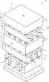
图1是根据本发明的一实施例的单个4T-2FC存储器单元的非-结构性图解示意图。1 is a non-structural schematic diagram of a single 4T-2FC memory cell according to an embodiment of the present invention.
图2是根据本发明的一实施例的图1示意图的多个4T-2FC存储器单元的阵列的一部分的图解混合示意性和结构性透视图。2 is a diagrammatic mixed schematic and structural perspective view of a portion of the array of multiple 4T-2FC memory cells of the schematic diagram of FIG. 1 in accordance with an embodiment of the present invention.
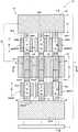
图3是通过图4和5中的线3-3截取的截面视图。FIG. 3 is a cross-sectional view taken through line 3-3 in FIGS. 4 and 5 .
图4是通过图3和5中的线4-4截取的截面视图。FIG. 4 is a cross-sectional view taken through line 4-4 in FIGS. 3 and 5 .
图5是通过图3和4中的线5-5截取的截面视图。FIG. 5 is a cross-sectional view taken through line 5-5 in FIGS. 3 and 4. FIG.
图6是根据本发明的一实施例的图1示意图的多个4T-2FC存储器单元的另一阵列的一部分的图解混合示意性和结构性截面视图,且对应于如图3结构中所展示的截面视图。6 is a diagrammatic mixed schematic and structural cross-sectional view of a portion of another array of the plurality of 4T-2FC memory cells of the FIG. 1 schematic, and corresponds to that shown in the FIG. 3 structure, in accordance with an embodiment of the present invention Sectional view.
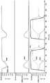
图7是展示根据图1到6的实施例的4T-2FC存储器单元的一些可能操作特性的电压对时间的曲线图。7 is a graph of voltage versus time showing some possible operating characteristics of a 4T-2FC memory cell according to the embodiments of FIGS. 1-6.
图8是根据本发明的一实施例的单个4T-2FC存储器单元的非结构性图解示意图。8 is a non-structural schematic diagram of a single 4T-2FC memory cell according to an embodiment of the present invention.
图9是根据本发明的一实施例的图8示意图的多个4T-2FC存储器单元的阵列的一部分的图解混合示意性和结构性透视图。9 is a diagrammatic mixed schematic and structural perspective view of a portion of the array of multiple 4T-2FC memory cells of the schematic diagram of FIG. 8 in accordance with an embodiment of the present invention.
图10是通过图11和12中的线10-10截取的截面视图。FIG. 10 is a cross-sectional view taken through line 10 - 10 in FIGS. 11 and 12 .
图11是通过图10和12中的线11-11截取的截面视图。FIG. 11 is a cross-sectional view taken through line 11 - 11 in FIGS. 10 and 12 .
图12是通过图10和11中的线12-12截取的截面视图。FIG. 12 is a cross-sectional view taken through line 12 - 12 in FIGS. 10 and 11 .
图13是根据本发明的一实施例的图8示意图的多个4T-2FC存储器单元的另一阵列的一部分的图解混合示意性和结构性截面视图,且对应于如图10结构中所展示的截面视图。13 is a diagrammatic mixed schematic and structural cross-sectional view of a portion of another array of the plurality of 4T-2FC memory cells of the FIG. 8 schematic, and corresponds to the structure shown in FIG. 10, in accordance with an embodiment of the present invention Sectional view.
图14是展示根据图8到13的实施例的4T-2FC存储器单元的一些可能操作特性的电压对时间的曲线图。14 is a graph of voltage versus time showing some possible operating characteristics of a 4T-2FC memory cell according to the embodiments of FIGS. 8-13.
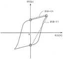
图15是铁电电容器的磁滞回线的曲线图。FIG. 15 is a graph of a hysteresis loop of a ferroelectric capacitor.
具体实施方式Detailed ways
本发明的实施例包括单个存储器单元,所述单个存储器单元个别地具有四个晶体管和两个铁电电容器(例如,在一些实施例中与单个存储器单元中的晶体管和电容器的总数一样,而不管其示意图,且在下文中被称为4T-2FC存储器单元)以及此类存储器单元的阵列。首先参考图1到6描述其第一实施例,其中图1是根据一些实施例的一个单个4T-2FC存储器单元MC0的示意图。Embodiments of the invention include a single memory cell that individually has four transistors and two ferroelectric capacitors (eg, in some embodiments the same as the total number of transistors and capacitors in a single memory cell, regardless of A schematic diagram thereof, and is hereinafter referred to as a 4T-2FC memory cell) and an array of such memory cells. A first embodiment thereof is first described with reference to Figures 1 through 6, wherein Figure 1 is a schematic diagram of a single 4T-2FC memory cell MC0 according to some embodiments.
参考图2到5,衬底构造10包括基底衬底11,所述基底衬底11可包含导电性/导体/导电(即,本文中以电气方式)、半导电性/半导体/半导电或绝缘性/绝缘体/绝缘(即,在本文中以电气方式)材料中的任何一或多种。各种材料已经竖向地形成在基底衬底11上方。材料可在图2到5所描绘的材料旁边、从图2到5所描绘的材料竖向向内或从图2到5所描绘的材料竖向向外。举例来说,集成电路的其它部分或完全制造的组件可设置在基底衬底11上方某处、围绕基底衬底11设置或设置在基底衬底11内。还可制造用于操作存储器单元阵列内的组件的控制和/或其它外围设备电路,且可或可不完全地或部分地在存储器阵列或子阵列内。此外,也可相对彼此独立地、先后地(in tandem)或以其它方式构制造和操作多个存储器子阵列。如此文件中所使用,“子阵列”也可被视为阵列。Referring to Figures 2-5,
构造10包括4T-2FC存储器单元(例如,MC0、MC1)的阵列13。图2到5中总共可见仅六个(图5)存储器单元MC0和MC1的部分,其中一阵列可能具有数千、数十万、数百万等相似构造的存储器单元MC*(符号“*”在本文中用作任何具体编号组件的通用替代)。阵列13包括行12和列14,包括多个铁电电容器(例如,FC0T、FC0B、FC1T、FC1B)。两个行内紧邻铁电电容器的对(例如,对FC0T、FC0B和对FC1T、FC1B)包括个别4T-2FC存储器单元MC*的两个铁电电容器。两个铁电电容器个别地包括第一电容器电极(例如,CBT0、CBB0、CBT1、CBB1)和第二电容器电极(例如,CP),其间具有铁电电容器绝缘体16。铁电电容器绝缘体16包括从其第一电容器电极CBT*或CBB*径向向外的环带18。第二电容器电极CP包括从铁电电容器绝缘体环带18径向向外的部分20(图5)。此外,在此实例实施例中,第二电容器电极CP是所有多个铁电电容器FC*T、FC*B的第二电容器电极且对所有多个铁电电容器FC*T、FC*B共用。
列14包括彼此列内紧邻的第一比较性数字线(例如,DLT0、DLT1)和第二比较性数字线(例如,DLB0、DLB1)的对(例如,对DLT0、DLB0和对DLT1、DLB1)。此类对可个别地连接到读取/感测放大器SA(图1,其构造可在阵列13的边缘处),所述读取/感测放大器SA可用来放大当存储器单元MC*被读存取时在数字线对上产生的差信号。
行12和列14包括短路晶体管(例如,MCBRT0、MCBRB0、MCBRT1、MCBRB2),所述短路晶体管个别地包括晶体管栅极28(图4),所述晶体管栅极28包括使短路晶体管中的多个沿着个别行12互连的个别短路控制线(例如,CBR0、CBR1、CBR2)的一部分。两个紧邻行内短路晶体管的对(例如,对MCBRT0、MCBRB0和对MCBRT1、MCBRB1)包括个别4T-2FC存储器单元MC*的第一两个晶体管。个别4T-2FC存储器单元MC*中的此类第一两个短路晶体管个别地直接电耦合到相应第一电容器电极CBT*、CBB*和共用第二电容器电极CP中的不同电容器电极且直接电耦合在所述不同电容器电极之间。
行12和列14包括选择晶体管(例如,MWL0T、MWL0B、MWL1T、MWL1B,且其可替代地可被视为存取晶体管),所述选择晶体管个别地包括晶体管栅极40(图4),所述晶体管栅极40包括使选择晶体管中的多个沿着个别行12互连的个别字线(例如,WL0、WL1、WL2)的一部分。两个紧邻行内选择晶体管的对(例如,对MWL0T、MWL0B和对MWL1T、MWL1B)包括个别4T-2FC存储器单元MC*的第二两个晶体管。个别4T-2FC存储器单元MC*中的此类第二两个选择晶体管个别地直接电耦合到相应第一电容器电极CBT*、CBB*中的不同第一电容器电极以及第一和第二比较性数字线的个别对(例如,DLT0/DLB0、DLT1/DLB1)的第一比较性数字线DLT*或第二比较性数字线DLB*中的不同比较性数字线且直接电耦合在所述不同第一电容器电极与所述不同比较性数字线之间。
(a)字线或(b)短路控制线中的一个在所有多个铁电电容器上方,而(a)或(b)中的另一个在所有多个铁电电容器下方。图2到5描绘一实施例,其中(b):短路控制线在所有多个铁电电容器上方。阵列13a的替代实施例构造10a在图6(类似于图3)中所展示,其中(a):字线在所有多个铁电电容器上方。已经在适当时使用上文所描述实施例的相同标号,其中用后缀“a”指示某些构造差异。如本文中相对于其它实施例所展示和/或描述的任何其它属性或方面可用于图6实施例。One of (a) the word line or (b) the shorted control line is above all of the plurality of ferroelectric capacitors, and the other of (a) or (b) is below all of the plurality of ferroelectric capacitors. Figures 2 to 5 depict an embodiment in which (b): the shorted control line is over all of the plurality of ferroelectric capacitors. An
在一个实施例中,所有第一和第二比较性数字线在具有字线的所有铁电电容器上方或下方。换句话说,在此实施例中,所有第一和第二比较性数字线在字线的上侧或下侧中的任一个位于上面的所有铁电电容器上方或下方,且如仅借助于实例相对于图2到5实施例和图6实施例中的每一个所展示。在一个此类实施例中,字线在所有铁电电容器下方且所有第一和第二比较性数字线在所有字线下方(例如,图2到5实施例)。在替代此类实施例中,字线在所有铁电电容器上方且所有第一和第二比较性数字线在所有字线上方(例如,图6实施例)。In one embodiment, all first and second comparative digit lines are above or below all ferroelectric capacitors having word lines. In other words, in this embodiment, all first and second comparative digit lines are either above or below all ferroelectric capacitors above on either the upper side or the lower side of the word line, and as by way of example only Illustrated with respect to each of the embodiments of FIGS. 2 to 5 and the embodiment of FIG. 6 . In one such embodiment, word lines are below all ferroelectric capacitors and all first and second comparative digit lines are below all word lines (eg, the FIGS. 2-5 embodiments). In alternative such embodiments, word lines are above all ferroelectric capacitors and all first and second comparative digit lines are above all word lines (eg, the FIG. 6 embodiment).
在一个实施例中且如所展示,短路晶体管和选择晶体管是竖向延伸的晶体管,且在一个此类实施例中是竖直的或在竖直10°内。在一个实施例中,4T-2FC存储器单元MC*个别地包括相对于彼此行内间隔开的第一竖向延伸的柱(例如,24)和第二竖向延伸的柱(例如,26)。在此实施例中,个别4T-2FC存储器单元MC*的短路晶体管和选择晶体管可被视为个别地包括源极/漏极区和其间的竖向延伸的沟道区。举例来说,图3和4展示短路晶体管MCBRT*、MCBRB*,所述短路晶体管MCBRT*、MCBRB*个别地包括源极/漏极区35、源极/漏极区CBT0、CBB0 CBT1、CBB1以及其间的竖向延伸的沟道区32。源极/漏极区35和第二电容器电极CP可被视为单个或集体电极,且其中所描绘的其两个竖向间隔开的CP部分在图2到6实施例中彼此直接电耦合(例如,通过示意性互连线25,其构造可在阵列13的边缘处)。此外,举例来说,个别4T-2FC存储器单元MC*的选择晶体管MWL*T、MWL*B个别地包括源极/漏极区37、源极/漏极区CBT0、CBB0、CBT1、CBB1以及其间的竖向延伸的沟道区33。短路晶体管MCBRT、MCBRB的沟道区32在一个层级36处彼此行内间隔开,且选择晶体管MWL*T、MWL*B的沟道区33以与层级36竖向间隔开的另一层级34彼此行内间隔开。In one embodiment and as shown, the shorting transistor and the select transistor are vertically extending transistors, and in one such embodiment are vertical or within 10° of vertical. In one embodiment, 4T-2FC memory cells MC* individually include a first vertically extending pillar (eg, 24) and a second vertically extending pillar (eg, 26) spaced in-row relative to each other. In this embodiment, the short and select transistors of the individual 4T-2FC memory cells MC* can be viewed as individually including source/drain regions and vertically extending channel regions therebetween. For example, Figures 3 and 4 show shorting transistors MCBRT*, MCBRB*, which individually include source/
第一柱24个别地包括个别4T-2FC存储器单元MC*的短路晶体管MCBRT*、MCBRB*中的一个和选择晶体管MWL*T、MWL*B中的一个的各自沟道区32、33。第一柱24还个别地包括个别4T-2FC存储器单元MC*的短路晶体管中的相应短路晶体管和选择晶体管中的相应选择晶体管的源极/漏极区。第一柱24另外个别地包括个别4T-2FC存储器单元MC*的两个铁电电容器中的一个的第一电容器电极CBBT*、CBBB*。第二柱26个别地包括个别4T-2FC存储器单元MC*的另一个短路晶体管和另一个选择晶体管的各自沟道区32、33。第二柱26还个别地包括个别4T-2FC存储器单元MC*的相应其它短路晶体管和相应其它选择晶体管的源极/漏极区。第二柱26另外个别地包括个别4T-2FC存储器单元MC*的两个铁电电容器中的另一个铁电电容器的第一电容器电极。The
如本文中相对于其它实施例所展示和/或描述的任何其它属性或方面可用于图1到5实施例。Any other attributes or aspects as shown and/or described herein with respect to other embodiments may be used with the Figures 1-5 embodiments.
接下来参考图8到12描述4T-2FC存储器单元MC*的阵列13b的替代实例实施例构造10b。已经在适当时使用上文所描述实施例的相同标号,用后缀“b”或用不同标号指示某些构造差异。构造10b与构造10的部分不同之处在于铁电电容器的第二电容器电极并不对所有多个铁电电容器共用。实际上,阵列13b具有彼此电隔离的个别4T-2FC存储器单元MC*(即,CP1和CP2并不直接彼此电耦合)的两个铁电电容器(例如,FC*T、FC*B)的第二电容器电极(例如,CP1、CP2)。个别4T-2FC存储器单元MC*的两个铁电电容器的第一电容器电极CBT*、CBB*也彼此电隔离,且例如如首先所描述实施例中所展示。正如所描述的两个竖向间隔开的CP1部分一样,所描绘的两个竖向间隔开的CP1部分直接彼此电耦合(例如,通过用于CP1部分的示意性互连线25和通过用于CP2部分的示意性互连线27,且其构造可在阵列13b的边缘处)。An alternate
另外,在构造10b中,列14包括列内紧邻第一比较性数字线(DLT0、DLT1)的对(例如,对DLT0、DLT1)和列内紧邻第二比较性数字线(DLB0、DLB1)的对(例如,对DLB0、DLB1)。个别存储器单元MC*包括第一比较性数字线DLT0或DLT1中的一个和第二比较性数字线DLB0或DLB1中的一个。因此,个别存储器单元MC*的所有组件并非如例如首先所描述实施例的构造10/10a中所展示的那样全部彼此行内紧邻。Additionally, in
行12和列14同样包括短路晶体管MCBRT*、MCBRB*,所述短路晶体管MCBRT*、MCBRB*个别地包括晶体管栅极28,所述晶体管栅极28包括使短路晶体管中的多个沿着个别行12互连的个别短路控制线CBR*的一部分。然而,个别行12中的短路晶体管的每一个其它短路晶体管的对(例如,对MCBRT0、MCBRB0和对MCBRT1、MCBRB1)包括个别4T-2FC存储器单元MC*的第一两个晶体管。个别4T-2FC存储器单元MC*中的第一两个短路晶体管个别地直接电耦合到相应第一电容器电极CBT*、CBB*中的不同第一电容器电极和相应第二电容器电极CP*、CP*中的不同第二电容器电极且直接电耦合在所述不同第一电容器电极与所述不同第二电容器电极之间。
行12和列14同样包括选择晶体管MWL*T、MWL*B,所述选择晶体管MWL*T、MWL*B个别地包括晶体管栅极40,所述晶体管栅极40包括使选择晶体管中的多个沿着个别行12互连的个别字线WL*的一部分。然而,个别行12中的选择晶体管的每一个其它选择晶体管的对(例如,对MWL0T、MWL0B和对MWL1T、MWL1B)包括个别4T-2FC存储器单元MC*的第二两个选择晶体管。个别4T-2FC存储器单元MC*中的第二两个选择晶体管个别地直接电耦合到相应第一电容器电极CBT*、CBB*中的不同第一电容器电极和相应第一或第二比较性数字线DLT*、DLB*中的比较性数字线且直接电耦合在所述不同第一电容器电极与所述不同比较性数字线之间。(a)字线或(b)短路控制线中的一个在所有铁电电容器上方,而(a)或(b)中的另一个在所有铁电电容器下方。图9到12描绘一实例实施例,其中(b):短路控制线在所有铁电电容器上方。图13展示一替代实例实施例,其中(a):字线在所有铁电电容器上方。已经在适当时使用上文所描述实施例的相同标号,其中用后缀“c”指示某些构造差异。如本文中所展示和/或描述的任何其它属性或方面可相对于图8到12的实施例和图13的实施例一起使用。
本发明的一些实施例包括4T-2FC存储器单元,而不管是否是图1示意图、图8示意图或某一其它示意图,且可包含此类4T-2FC存储器单元的阵列。在一个此类实施例中,4T-2FC存储器单元包括第一、第二、第三和第四晶体管(例如,分别为MCBRT0、MCBRB0、MWL0T、MWL0B)。4T-2FC存储器单元包括第一和第二铁电电容器(例如,分别为FC0T、FC0B),所述第一和第二铁电电容器个别地具有在两个竖向间隔开的层级(例如,层级44、层级46)处的一个电容器电极(例如,图1示意图中的CP、图8示意图中的CP*)。铁电电容器绝缘体(例如,16)介于在两个层级(例如,构造10中的44)处的一个电容器电极与另一电容器电极(例如,CBT*、CBB*)之间,且没有铁电电容器绝缘体介于在两个层级中的另一个(例如,构造10中的46,至少是因为CBT*和CBB*都不在层级46内的任何位置)中的一个电容器电极与另一电容器电极之间。Some embodiments of the invention include 4T-2FC memory cells, whether the FIG. 1 schematic, the FIG. 8 schematic, or some other schematic, and may include arrays of such 4T-2FC memory cells. In one such embodiment, the 4T-2FC memory cell includes first, second, third, and fourth transistors (eg, MCBRT0, MCBRB0, MWLOT, MWLOB, respectively). The 4T-2FC memory cell includes first and second ferroelectric capacitors (eg, FCOT, FC0B, respectively) that individually have levels (eg, levels of 44. One capacitor electrode at level 46) (eg, CP in the schematic diagram of FIG. 1, CP* in the schematic diagram of FIG. 8). A ferroelectric capacitor insulator (eg, 16) is interposed between one capacitor electrode and the other capacitor electrode (eg, CBT*, CBB*) at two levels (eg, 44 in configuration 10), and no ferroelectric A capacitor insulator is interposed between one capacitor electrode and the other in the other of the two levels (eg, 46 in
在一个实施例中,第一、第二、第三和第四晶体管个别地包括晶体管栅极(例如,28、40),其中栅极中的一个(例如,构造10中的28)竖向地介于两个竖向间隔开的层级之间。在一个此类实施例中,栅极中的另一个(例如,构造10中的40)并不竖向地介于两个竖向间隔开的层级之间。在一个实施例中,晶体管栅极中的多个(例如,构造10中的28)竖向地介于两个竖向间隔开的层级之间。在一个此类实施例中,有且仅有两个晶体管栅极竖向地介于两个竖向间隔开的层级之间。在一个实施例中,第一、第二、第三和第四晶体管中的两个是直接电耦合到相应一个电容器电极中的不同电容器电极和另一电容器电极中的不同电容器电极且直接电耦合在相应一个电容器电极中的不同电容器电极与另一电容器电极中的不同电容器电极之间的短路晶体管(例如,MCBR0T、MCBR0B)。In one embodiment, the first, second, third and fourth transistors individually include transistor gates (eg, 28, 40), wherein one of the gates (eg, 28 in construction 10) is vertically between two vertically spaced levels. In one such embodiment, the other of the gates (eg, 40 in construction 10) is not vertically interposed between the two vertically spaced levels. In one embodiment, a plurality of transistor gates (eg, 28 in construction 10) are vertically interposed between two vertically spaced levels. In one such embodiment, there are and only two transistor gates vertically interposed between the two vertically spaced levels. In one embodiment, two of the first, second, third and fourth transistors are directly electrically coupled to and directly electrically coupled to different ones of the respective one capacitor electrodes and the other capacitor electrodes Shorting transistors (eg, MCBR0T, MCBR0B) between different ones of the respective one capacitor electrodes and different ones of the other capacitor electrodes.
在一个实施例中,阵列(例如,13、13a)包括4T-2FC存储器单元作为相对于彼此具有相似构造的多个4T-2FC存储器单元的一个存储器单元,且其中一个电容器电极是多个4T-2FC存储器单元的所有铁电电容器的一个电容器电极且对所有铁电电容器共用。在另一实施例中,阵列(例如,13b、13c)包括4T-2FC存储器单元作为相对于彼此具有相似构造的多个4T-2FC存储器单元的一个存储器单元。在此实施例中,个别4T-2FC存储器单元中的第一和第二铁电电容器的一个电容器电极彼此电隔离。在此实施例中,个别4T-2FC存储器单元中的第一和第二铁电电容器的另一电容器电极彼此电隔离。In one embodiment, the array (eg, 13, 13a) includes a 4T-2FC memory cell as one memory cell of a plurality of 4T-2FC memory cells of similar construction relative to each other, and wherein one capacitor electrode is a plurality of 4T-2FC memory cells One capacitor electrode for all ferroelectric capacitors of a 2FC memory cell and is common to all ferroelectric capacitors. In another embodiment, the array (eg, 13b, 13c) includes a 4T-2FC memory cell as one memory cell of a plurality of 4T-2FC memory cells of similar construction relative to each other. In this embodiment, one capacitor electrode of the first and second ferroelectric capacitors in an individual 4T-2FC memory cell is electrically isolated from each other. In this embodiment, the other capacitor electrodes of the first and second ferroelectric capacitors in the individual 4T-2FC memory cells are electrically isolated from each other.
可使用如本文中所展示和/或描述的任何其它属性或方面。Any other attributes or aspects as shown and/or described herein may be used.
本发明的额外实施例包括4T-2FC存储器单元,而不管是否是图1示意图、图8示意图或某一其它示意图,且可包含此类4T-2FC存储器单元的阵列。在一个此类实施例中,4T-2FC存储器单元包括第一、第二、第三和第四晶体管(例如,分别为MCBRT0、MCBRB0、MWL0T、MWL0B),所述第一、第二、第三和第四晶体管个别地包括晶体管栅极(例如,28、40)。4T-2FC存储器单元包括第一和第二铁电电容器(例如,分别为FC0T、FC0B),所述第一和第二铁电电容器个别地具有竖向地介于第一、第二、第三和第四晶体管的晶体管栅极之间的一个电容器电极(例如,CBT0、CBB0)。在一个实施例中,第一和第二铁电电容器个别地具有另一电容器电极(例如,CP、CP1、CP2),所述另一电容器电极的某一部分(例如,在构造10中的层级44内)竖向地介于第一、第二、第三和第四晶体管的晶体管栅极之间。在一个实施例中,第一和第二铁电电容器个别地具有另一电容器电极(例如,CP、CP1、CP2),所述另一电容器电极的仅一部分(例如,在构造10中的层级44内)竖向地介于第一、第二、第三和第四晶体管的晶体管栅极之间。在一个实施例中,阵列(例如,13、13a、13b、13c)包括4T-2FC存储器单元作为相对于彼此具有相似构造的多个4T-2FC存储器单元的一个存储器单元。可使用如本文中所展示和/或描述的任何其它属性或方面。Additional embodiments of the invention include 4T-2FC memory cells, whether the FIG. 1 schematic, the FIG. 8 schematic, or some other schematic, and may include arrays of such 4T-2FC memory cells. In one such embodiment, the 4T-2FC memory cell includes first, second, third, and fourth transistors (eg, MCBRT0, MCBRB0, MWLOT, MWLOB, respectively), the first, second, third and fourth transistors individually include transistor gates (eg, 28, 40). The 4T-2FC memory cell includes first and second ferroelectric capacitors (eg, FCOT, FCOB, respectively), the first and second ferroelectric capacitors individually having vertically interposed between the first, second, and third ferroelectric capacitors. A capacitor electrode (eg, CBT0, CBB0) between the transistor gate of the fourth transistor. In one embodiment, the first and second ferroelectric capacitors individually have another capacitor electrode (eg, CP, CP1 , CP2 ), some portion of the other capacitor electrode (eg,
本发明的额外实施例包括4T-2FC存储器单元,而不管是否是图1示意图、图8示意图或某一其它示意图,且可包含此类4T-2FC存储器单元的阵列。在一个此类实施例中,4T-2FC存储器单元包括第一、第二、第三和第四晶体管(例如,分别为MCBRT0、MCBRB0、MWL0T、MWL0B)。4T-2FC存储器单元包括第一和第二铁电电容器(例如,分别为FC0T、FC0B),所述第一和第二铁电电容器个别地包括第一和第二电容器电极(例如,分别为CBT0、CBB0和CP、CP1、CP2),所述第一和第二电容器电极在其间具有铁电电容器绝缘体(例如,16)。第一电容器电极包括竖向延伸的柱(例如,24、26)。铁电电容器绝缘体包括从第一电容器电极径向向外的环带(例如,18)。第二电容器电极包括从铁电-电容器-绝缘体环带径向向外的部分(例如,20)。在一个实施例中,柱的导电材料(例如,CBT*、CBB*的材料)在直径上完整地跨越所有柱延伸。Additional embodiments of the invention include 4T-2FC memory cells, whether the FIG. 1 schematic, the FIG. 8 schematic, or some other schematic, and may include arrays of such 4T-2FC memory cells. In one such embodiment, the 4T-2FC memory cell includes first, second, third, and fourth transistors (eg, MCBRT0, MCBRB0, MWLOT, MWLOB, respectively). The 4T-2FC memory cell includes first and second ferroelectric capacitors (eg, FCOT, FC0B, respectively) that individually include first and second capacitor electrodes (eg, CBT0, respectively) , CBB0 and CP, CP1, CP2), the first and second capacitor electrodes have a ferroelectric capacitor insulator (eg, 16) therebetween. The first capacitor electrode includes vertically extending posts (eg, 24, 26). The ferroelectric capacitor insulator includes an annulus (eg, 18) radially outward from the first capacitor electrode. The second capacitor electrode includes a portion (eg, 20) radially outward from the ferroelectric-capacitor-insulator annulus. In one embodiment, the conductive material of the posts (eg, material of CBT*, CBB*) extends diametrically completely across all posts.
在一个实施例中,第一、第二、第三和第四晶体管个别地包括晶体管栅极(例如,28、40)。第一、第二、第三和第四晶体管中的两个(例如,构造10中的MCBRT0、MCBRB0)的栅极(例如,构造10中的28)在第二电容器电极的从铁电-电容器-绝缘体环带径向向外的部分上方。第一、第二、第三和第四晶体管中的另外两个(例如,构造10中的MWL0T、MWL0B)的栅极(例如,构造10中的40)在第二电容器电极的从铁电-电容器-绝缘体环带径向向外的部分下方。In one embodiment, the first, second, third and fourth transistors individually include transistor gates (eg, 28, 40). The gates (eg, 28 in configuration 10) of two of the first, second, third, and fourth transistors (eg, MCBRT0, MCBRB0 in configuration 10) are in the second capacitor electrode from the ferroelectric-capacitor - Above the radially outward portion of the insulator annulus. The gates (eg, 40 in configuration 10) of the other two of the first, second, third, and fourth transistors (eg, MWL0T, MWLOB in configuration 10) are in the second capacitor electrode from the ferroelectric- Below the radially outward portion of the capacitor-insulator annulus.
可使用如本文中所展示和/或描述的任何其它属性或方面。Any other attributes or aspects as shown and/or described herein may be used.
本发明的额外实施例包括4T-2FC存储器单元,而不管是否是图1示意图、图8示意图或某一其它示意图,且可包含此类4T-2FC存储器单元的阵列。在一个此类实施例中,4T-2FC存储器单元包括第一和第二侧向间隔开和竖向延伸的柱(例如,分别为24、26)。4T-2FC存储器单元包括第一和第二铁电电容器(例如,分别为FC0T、FC0B),所述第一和第二铁电电容器个别地包括第一和第二电容器电极(例如,分别为CBT0、CBB0和CP、CP1、CP2),所述第一和第二电容器电极在其间具有铁电电容器绝缘体(例如,16)。4T-2FC存储器单元包括第一、第二、第三和第四竖向延伸的晶体管(例如,分别为MCBRT0、MCBRB0、MWL0T、MWL0B),所述第一、第二、第三和第四竖向延伸的晶体管个别地包括源极/漏极区(例如,35、CBT0、CBB0、37)、介于源极/漏极区之间的竖向延伸的沟道区(例如,32、33)以及可操作地接近于沟道区的晶体管栅极(例如,28、40)(例如,栅极绝缘体17介于沟道与栅极之间)。第一和第二晶体管(例如,构造10中的MCBRT0、MCBRB0)的沟道区(例如,构造10中的32)在第二电容器电极上方彼此侧向邻近。第三和第四晶体管(例如,构造10中的MWL0T、MWL0B)的沟道区(例如,构造10中的33)在第二电容器电极下方彼此侧向邻近。第一柱包括第一和第三晶体管的源极/漏极区和沟道区。第一柱包括第一铁电电容器的第一电容器电极。第二柱包括第二和第四晶体管的源极/漏极区和沟道区。第二柱包括第二铁电电容器的第一电容器电极。可使用如本文中所展示和/或描述的任何其它属性或方面。Additional embodiments of the invention include 4T-2FC memory cells, whether the FIG. 1 schematic, the FIG. 8 schematic, or some other schematic, and may include arrays of such 4T-2FC memory cells. In one such embodiment, the 4T-2FC memory cell includes first and second laterally spaced and vertically extending pillars (eg, 24, 26, respectively). The 4T-2FC memory cell includes first and second ferroelectric capacitors (eg, FCOT, FC0B, respectively) that individually include first and second capacitor electrodes (eg, CBT0, respectively) , CBB0 and CP, CP1, CP2), the first and second capacitor electrodes have a ferroelectric capacitor insulator (eg, 16) therebetween. The 4T-2FC memory cell includes first, second, third, and fourth vertically extending transistors (eg, MCBRT0, MCBRB0, MWLOT, MWLOB, respectively) that are The extending transistors individually include source/drain regions (eg, 35, CBT0, CBB0, 37), vertically extending channel regions (eg, 32, 33) between the source/drain regions and transistor gates (eg, 28, 40) operatively proximate to the channel region (eg,
在一些实施例中,竖向延伸的特征中的任何一或多个被形成为竖直的或在竖直10°内。In some embodiments, any one or more of the vertically extending features are formed vertical or within 10° of vertical.
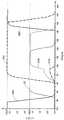
图7是展示根据图1到6的实施例的4T-2FC存储器单元的一些可能的操作特性的电压对时间的曲线图。更具体地说,图7是图1到6存储器单元MC0的读取和写入循环的时序图。由于可能不允许跨铁电电容器FC0T和FC0B的电压差,因此平衡信号CBR0在备用期间处于VCCP。在循环开始时,平衡CBR0被关闭以使单元板CP与铁电电容器FC0T、CBT0的另一节点断开连接,所述另一节点与单元板CP处于相同电势。数字线DLT0和DLB0在备用期间被预充电到接地。一旦CBR0被关闭,数字线就与地面断开连接且变得是电压浮动的,且单元板CP被升高到VMSA,同时CBT0和CBB0两者由于充分大于CBT0或CBB0的寄生电容值的铁电电容器的电容而被拉升到类似于单元板CP的层级的层级。接着,为了存取铁电电容器FC0T和FC0B,字线WL0被升高到高达VCCP层级。一旦WL0达到选择晶体管MWL0T和MWL0B的阈值电压,分别在数字线DLT0、DLB0与铁电电容器FC0T、FC0B之间就会发生电荷转移。数字线电压根据其相对电容形成。铁电电容器的两个电容0或1可通过如图15中所展示的两个线性电容器C0或C1中的一个进行估算。因此,在数字线DLT0和DLB0上形成的电压可以是两个值V0或V1中的一个:7 is a graph of voltage versus time showing some possible operating characteristics of a 4T-2FC memory cell according to the embodiments of FIGS. 1-6. More specifically, FIG. 7 is a timing diagram of the read and write cycles of the memory cell MC0 of FIGS. 1 through 6 . Since the voltage difference across the ferroelectric capacitors FC0T and FC0B may not be allowed, the balanced signal CBR0 is at VCCP during standby. At the beginning of the cycle, the balancing CBR0 is closed to disconnect the cell plate CP from the other node of the ferroelectric capacitors FCOT, CBT0, which is at the same potential as the cell plate CP. The digital lines DLT0 and DLB0 are precharged to ground during standby. Once CBR0 is turned off, the digit line is disconnected from ground and becomes voltage floating, and the cell board CP is raised to VMSA, while both CBT0 and CBB0 due to ferroelectricity sufficiently larger than the parasitic capacitance value of CBT0 or CBB0 The capacitance of the capacitor is pulled up to a level similar to that of the cell board CP. Next, to access the ferroelectric capacitors FC0T and FC0B, the word line WL0 is raised up to the VCCP level. Once WL0 reaches the threshold voltages of select transistors MWL0T and MWL0B, charge transfer occurs between digit lines DLT0, DLB0 and ferroelectric capacitors FC0T, FC0B, respectively. The digital line voltage is formed according to its relative capacitance. The two
V数字线=V0={C0/(C0+C数字线)}x VMSA (如果单元数据是0)Vdigit line = V0 = {C0/(C0+Cdigit line )} x VMSA (if cell data is 0)
V数字线=V1={C1/(C1+C数字线)}x VMSA (如果单元数据是1)Vdigit line = V1 = {C1/(C1+Cdigit line )} x VMSA (if cell data is 1)
电容器FC0T和FC0B上的数据彼此互补。因此,如果FC0T是1,那么FC0B是0,且反之亦然。一旦DLT0与DLB0之间形成的电压差稳定,读取/感测放大器SA就将所述形成的电压差驱动到满刻度电压VMSA和接地层级且读取数据将最终被如下往回写入到电容器:当单元板CP为高时,DLT0被固定到接地层级且单元板CP是VMSA,接着数据0被写入到电容器FC0T。另一方面,当单元板CP接地且数字线DLB0处于VMSA时,互补数据1被写入到电容器FC0B。在数据被往回写入到电容器之后,数字线和单元板CP被驱动到接地且平衡信号CBR0接通以确保跨铁电电容器FC0T和FC0B的顶部和底部节点无电压差,可能需要无电压差以避免电容器由于印记或干扰或保留问题而丢失电容器中的信号。在循环结束时,字线WL0被关闭到接地层级。The data on capacitors FC0T and FC0B are complementary to each other. Thus, if FC0T is 1, then FC0B is 0, and vice versa. Once the voltage difference formed between DLT0 and DLB0 stabilizes, the read/sense amplifier SA drives the formed voltage difference to the full scale voltage VMSA and ground level and the read data will eventually be written back to the capacitor as follows : When cell board CP is high, DLT0 is pinned to the ground plane and cell board CP is VMSA, then
图14是展示根据图8到13的实施例的4T-2FC存储器单元MC0的一些可能的操作特性的电压对时间的曲线图。图14的顶部曲线图表示连接到晶体管MWL0B的电容器FC0B的电极的电势曲线。图14的中间曲线图表示连接到晶体管MWL0T的电容器FC0T的电极的电势曲线。图14的底部曲线图表示字线WL0以及所展示的两次连续读取-存取的电势曲线,由此逻辑“0”被存储在电容器FC0T、FC0B中。在对存储器单元进行读取-存取之前,两个数字线DLT0、DLB0被预充电到共用偏置电势VMSA=1.6V。此对应于两个板电势CP1=0V和约CP=3.2V的平均值。字线WL0接着用正边沿变得有源。晶体管MWL0T、MWL0B由此被切换成“接通”以导电,从而使得数字线DLT0、DLB0与电容器FC0T、FC0B之间发生电荷均衡。就存储的逻辑“0”而言,数字线DLT0的电势稍微减小,且数字线DLB0的电势稍微增大。接下来,读取/感测放大器SA被启动,由此数字线对DLT0、DLB0上的差信号被放大。读取-存取以字线WL0上的电势的负边沿结束。14 is a graph of voltage versus time showing some possible operating characteristics of a 4T-2FC memory cell MC0 according to the embodiments of FIGS. 8-13. The top graph of Figure 14 represents the potential profile of the electrode of capacitor FCOB connected to transistor MWLOB. The middle graph of FIG. 14 represents the potential curve of the electrode of the capacitor FCOT connected to the transistor MWLOT. The bottom graph of Figure 14 represents word line WL0 and the potential curve shown for two consecutive read-accesses, whereby a logic "0" is stored in capacitors FCOT, FCOB. The two digit lines DLT0, DLB0 are precharged to a common bias potential VMSA=1.6V prior to read-access to the memory cell. This corresponds to the average of the two plate potentials CP1=0V and about CP=3.2V. Word line WL0 then becomes active with the positive edge. The transistors MWL0T, MWL0B are thus switched "on" to conduct so that charge equalization occurs between the digit lines DLT0, DLB0 and the capacitors FC0T, FC0B. Regarding the stored logic "0", the potential of the digit line DLT0 is slightly decreased, and the potential of the digit line DLB0 is slightly increased. Next, the read/sense amplifier SA is activated, whereby the difference signal on the digit line pair DLT0, DLB0 is amplified. The read-access ends with the negative edge of the potential on word line WLO.
在此文件中,除非另外指明,否则“竖向”、“更高”、“上部”、“下部”、“顶部”、“顶上”、“底部”、“上方”、“下方”、“在…下方”、“在…之下”、“向上”和“向下”大体上参照竖直方向。“水平”是指沿着主衬底表面的一般方向(即,10度内)且可相对于在制造期间处理的衬底,且竖直是大体上与水平正交的方向。对“恰好水平”的提及是沿着主衬底表面的方向(即,从所述主衬底表面无度数)且可相对于在制造期间处理的衬底。此外,如本文中所使用的“竖直”和“水平”是相对于彼此的大体上垂直方向,且与三维空间中衬底的定向无关。另外,“竖向延伸的”和“竖向地延伸”是指从恰好水平偏离至少45°的方向。此外,相对于场效应晶体管的“竖向地延伸”和“竖向延伸的”是参照晶体管的沟道长度的定向,在源极/漏极区之间操作时电流沿着所述晶体管的沟道长度流动。对于双极结晶体管,“竖向地延伸”和“竖向延伸的”是参照底座长度的定向,在发射极与集电极之间操作时电流沿着所述基极长度流动。In this document, unless otherwise indicated, "vertical", "higher", "upper", "lower", "top", "above", "bottom", "above", "below", " "Below", "under", "up" and "down" generally refer to the vertical direction. "Horizontal" refers to the general direction (ie, within 10 degrees) along the main substrate surface and relative to the substrate that can be handled during fabrication, and vertical is the direction generally orthogonal to horizontal. References to "exactly horizontal" are along the direction of the main substrate surface (ie, no degrees from the main substrate surface) and relative to the substrate that can be handled during fabrication. Furthermore, "vertical" and "horizontal" as used herein are generally vertical directions relative to each other and are independent of the orientation of the substrate in three-dimensional space. Additionally, "vertically extending" and "vertically extending" refer to directions that deviate from exactly horizontal by at least 45°. Furthermore, "vertically extending" and "vertically extending" with respect to a field effect transistor refer to the orientation of the channel length of the transistor along which the current flows when operating between the source/drain regions. track length flow. For bipolar junction transistors, "vertically extending" and "vertically extending" are orientations with reference to the length of the base along which current flows when operating between the emitter and collector.
此外,“正上方”、“正下方”和“正下面”要求两个所论述区/材料/组件相对彼此具有至少一定的侧向重叠(即,水平地)。而且,使用前面没有“正”的“上方”仅要求在另一所论述区/材料/组件上方的所论述区/材料/组件的某一部分从另一所论述区/材料/组件的竖向向外(即,与两个所论述区/材料/组件是否存在任何侧向重叠无关)。类似地,使用前面没有“正”的“下方”仅要求在另一所论述区/材料/组件下方/下面的所论述区/材料/组件的某一部分在另一所论述区/材料/组件的竖向内侧(即,与两个所论述区/材料/组件柱是否存在任何侧向重叠无关)。Furthermore, "directly above", "directly below" and "directly below" require that the two discussed regions/materials/components have at least some lateral overlap (ie, horizontally) with respect to each other. Moreover, the use of "above" without the preceding "positive" only requires that a portion of a discussed area/material/component above another discussed area/material/component is vertically oriented from another discussed area/material/component Outside (ie, regardless of whether there is any lateral overlap between the two discussed regions/materials/components). Similarly, the use of "below" without "positive" before it only requires that some portion of the discussed area/material/component below/below another discussed area/material/component is within the other discussed area/material/component Vertically inboard (ie, regardless of whether there is any lateral overlap of the two zones/materials/component columns in question).
本文中所描述的材料、区和结构中的任一个可以是均匀的或非均匀的,且无论如何在其上覆的任何材料上方可以是连续的或不连续的。此外,除非另外指明,否则可使用任何合适的或尚待开发的技术来形成每种材料,所述技术的实例是原子层沉积、化学气相沉积、物理气相沉积、外延生长、扩散掺杂和离子注入。Any of the materials, regions and structures described herein may be uniform or non-uniform, and in any event may be continuous or discontinuous over any material overlying it. Furthermore, unless otherwise specified, each material may be formed using any suitable or yet to be developed technique, examples of which are atomic layer deposition, chemical vapor deposition, physical vapor deposition, epitaxial growth, diffusion doping, and ionization injection.
另外,单独使用的“厚度”(前面无方向性形容词)被定义为从具有不同组分的紧邻材料或紧邻区的最接近表面垂直穿过给定材料或区的平均直线距离。另外,本文中所描述的各种材料或区可具有大体上恒定的厚度或具有可变的厚度。如果具有可变厚度,那么除非另外指明,否则厚度是指平均厚度,且所述材料或区由于厚度可变而将具有某一最小厚度和某一最大厚度。如本文中所使用,“不同组分”仅要求两个所论述材料或区的可直接抵靠彼此的那些部分在化学上和/或在物理上不同,例如在所述材料或区不均匀的情况下。如果两个所论述材料或区并未直接抵靠彼此,那么在所述材料或区不均匀的情况下,“不同组分”仅要求两个所论述材料或区的最接近于彼此的那些部分在化学上和/或在物理上不同。在此文件中,当所论述材料、区或结构相对彼此存在至少某一物理接触时,一材料、区或结构“直接抵靠”另一材料、区或结构。相比之下,前面没有“正”的“在…上方”、“在…上”、“邻近”、“沿着”和“抵靠”涵盖“直接抵靠”以及其中介入材料、区或结构使得所论述材料、区或结构相对于彼此无物理接触的构造。Additionally, "thickness" (preceded by non-directional adjective), used alone, is defined as the average straight-line distance perpendicular to a given material or region from the closest surface of immediately adjacent materials or regions having different compositions. Additionally, the various materials or regions described herein can have a substantially constant thickness or have a variable thickness. If having a variable thickness, unless otherwise specified, the thickness refers to the average thickness, and the material or region will have a certain minimum thickness and a certain maximum thickness due to the variable thickness. As used herein, "different components" require only those parts of the two discussed materials or regions that are chemically and/or physically different, such as where the materials or regions are not uniform, that may directly abut each other. case. If the two materials or regions in question are not directly against each other, then "different compositions" only require those parts of the two materials or regions in question that are closest to each other where the materials or regions are not homogeneous chemically and/or physically different. In this document, a material, region or structure is "directly abutted" against another material, region or structure when the materials, regions or structures in question are in at least some physical contact with respect to each other. In contrast, "above", "on", "adjacent", "along" and "abut" without "positive" before cover "directly abut" and intervening materials, regions or structures therein A configuration such that the materials, regions or structures in question are not in physical contact with each other.
在本文中,如果在正常操作中,电流能够从一个区域/材料/组件连续流动到另一区域/材料/组件,且在充足地产生亚原子正和/或负电荷时主要通过所述亚原子正和/或负电荷的移动来进行流动,那么所述区域/材料/组件相对于彼此“电耦合”。另一电子组件可在所述区/材料/组件之间且电耦合到所述区/材料/组件。相比之下,当区/材料/组件被称为“直接电耦合”时,直接电耦合的区/材料/组件之间没有介入的电子组件(例如,没有二极管、晶体管、电阻器、换能器、交换器、熔断器等)。In this context, if in normal operation, current can flow continuously from one region/material/component to another region/material/component, and mainly through the subatomic positive and/or negative subatomic charges when sufficient to generate the subatomic positive and/or negative charges and/or movement of negative charges to flow, then the regions/materials/components are "electrically coupled" with respect to each other. Another electronic component may be between and electrically coupled to the regions/materials/components. In contrast, when regions/materials/components are referred to as "directly electrically coupled," there are no intervening electronic components (eg, no diodes, transistors, resistors, transducers, etc.) between the regions/materials/components that are directly electrically coupled switches, switches, fuses, etc.).
另外,“金属材料”是元素金属、两种或多于两种元素金属的混合物或合金以及任何导电金属化合物中的任一个或组合。Additionally, a "metallic material" is any one or combination of an elemental metal, a mixture or alloy of two or more elemental metals, and any conductive metal compound.
在此文件中使用“行”和“列”是为了方便区分一个系列或定向的特征与另一系列或定向的特征且组件已经或将要沿着所述“行”和“列”形成。“行”和“列”相对于与功能无关的任何系列的区、组件和/或特征同义地使用。无论如何,行可以是相对于彼此直的和/或弯曲和/或平行和/或不平行,列可同样如此。此外,行和列可相对于彼此以90°或者以一或多个其它角度相交。The use of "rows" and "columns" in this document is for convenience in distinguishing one series or orientation of features from another series or orientation of features along which components have been or will be formed. "Row" and "column" are used synonymously with respect to any series of regions, components and/or features unrelated to function. In any event, the rows may be straight and/or curved and/or parallel and/or non-parallel with respect to each other, as may the columns. Furthermore, the rows and columns may intersect at 90° with respect to each other or at one or more other angles.
根据规定,已经就结构和方法特征而言以更具体或更不具体的语言描述了本文中所公开的主题。然而,应理解,权利要求书不限于所展示和描述的具体特征,因为本文中所公开的装置包括实例实施例。因此,权利要求书具有如书面所说明的全部范围,且应根据等效物原则恰当地进行解释。As required, the subject matter disclosed herein has been described in terms of structural and methodological features in terms of more specific or less specific language. It is to be understood, however, that the claims are not limited to the specific features shown and described, as the apparatus disclosed herein includes example embodiments. Accordingly, the claims have the full scope as they are written, and are to be properly construed in accordance with the doctrine of equivalents.
Claims (10)
Priority Applications (1)
| Application Number | Priority Date | Filing Date | Title |
|---|---|---|---|
| CN202211013284.9ACN115440264A (en) | 2017-08-22 | 2018-08-21 | Memory cell and memory cell array |
Applications Claiming Priority (2)
| Application Number | Priority Date | Filing Date | Title |
|---|---|---|---|
| US201762548799P | 2017-08-22 | 2017-08-22 | |
| US62/548,799 | 2017-08-22 |
Related Child Applications (1)
| Application Number | Title | Priority Date | Filing Date |
|---|---|---|---|
| CN202211013284.9ADivisionCN115440264A (en) | 2017-08-22 | 2018-08-21 | Memory cell and memory cell array |
Publications (2)
| Publication Number | Publication Date |
|---|---|
| CN109427382A CN109427382A (en) | 2019-03-05 |
| CN109427382Btrue CN109427382B (en) | 2022-09-09 |
Family
ID=65437879
Family Applications (2)
| Application Number | Title | Priority Date | Filing Date |
|---|---|---|---|
| CN201810954519.1AActiveCN109427382B (en) | 2017-08-22 | 2018-08-21 | Memory cell and memory cell array |
| CN202211013284.9APendingCN115440264A (en) | 2017-08-22 | 2018-08-21 | Memory cell and memory cell array |
Family Applications After (1)
| Application Number | Title | Priority Date | Filing Date |
|---|---|---|---|
| CN202211013284.9APendingCN115440264A (en) | 2017-08-22 | 2018-08-21 | Memory cell and memory cell array |
Country Status (2)
| Country | Link |
|---|---|
| US (3) | US10679687B2 (en) |
| CN (2) | CN109427382B (en) |
Families Citing this family (8)
| Publication number | Priority date | Publication date | Assignee | Title |
|---|---|---|---|---|
| JP2021048193A (en)* | 2019-09-17 | 2021-03-25 | キオクシア株式会社 | Semiconductor storage device |
| TWI882001B (en)* | 2019-10-31 | 2025-05-01 | 日商半導體能源研究所股份有限公司 | Semiconductor device and electronic device |
| US11114153B2 (en)* | 2019-12-30 | 2021-09-07 | Taiwan Semiconductor Manufacturing Co., Ltd. | SRAM devices with reduced coupling capacitance |
| US12048165B2 (en)* | 2020-06-26 | 2024-07-23 | Intel Corporation | Ferroelectric capacitors and methods of fabrication |
| KR102744282B1 (en)* | 2020-08-03 | 2024-12-19 | 에스케이하이닉스 주식회사 | Semiconductor device and manufacturing method of semiconductor device |
| US11706999B2 (en)* | 2021-01-13 | 2023-07-18 | Taiwan Semiconductor Manufacturing Co., Ltd. | Semiconductor device and manufacturing method of semiconductor device |
| KR20220149216A (en)* | 2021-04-30 | 2022-11-08 | 에스케이하이닉스 주식회사 | Memory cell and semiconductor memory dedvice with the same |
| CN118301940A (en)* | 2023-01-03 | 2024-07-05 | 华为技术有限公司 | Memory array, electronic equipment, memory and manufacturing method thereof |
Citations (4)
| Publication number | Priority date | Publication date | Assignee | Title |
|---|---|---|---|---|
| US6011285A (en)* | 1998-01-02 | 2000-01-04 | Sharp Laboratories Of America, Inc. | C-axis oriented thin film ferroelectric transistor memory cell and method of making the same |
| EP1475804A2 (en)* | 1999-06-02 | 2004-11-10 | Kabushiki Kaisha Toshiba | Ferroelectric memory and semiconductor memory |
| CN1819205A (en)* | 2004-11-30 | 2006-08-16 | 因芬尼昂技术股份公司 | Transistor array for semiconductor memory devices and method for fabricating a vertical channel transistor array |
| CN101000926A (en)* | 2007-01-08 | 2007-07-18 | 电子科技大学 | Ferroelectric field effect transistor storage device structure and preparation method |
Family Cites Families (20)
| Publication number | Priority date | Publication date | Assignee | Title |
|---|---|---|---|---|
| US5381364A (en) | 1993-06-24 | 1995-01-10 | Ramtron International Corporation | Ferroelectric-based RAM sensing scheme including bit-line capacitance isolation |
| US6256220B1 (en)* | 1997-09-15 | 2001-07-03 | Celis Semiconductor Corporation | Ferroelectric memory with shunted isolated nodes |
| US6316801B1 (en)* | 1998-03-04 | 2001-11-13 | Nec Corporation | Semiconductor device having capacitive element structure and multilevel interconnection structure and method of fabricating the same |
| DE19952311B4 (en) | 1999-10-29 | 2006-07-13 | Infineon Technologies Ag | Integrated memory with memory cells of 2-transistor / 2-capacitor type |
| JP2002289729A (en) | 2000-04-10 | 2002-10-04 | Ngk Spark Plug Co Ltd | Pin standing resin substrate, method for manufacturing pin standing resin substrate, pin and method for manufacturing pin |
| JP2002259729A (en) | 2001-02-27 | 2002-09-13 | Mitsubishi Shoji Plast Kk | Goods sales method and system using network |
| JP2002313100A (en)* | 2001-04-17 | 2002-10-25 | Toshiba Corp | Ferroelectric memory and test method therefor |
| US6744654B2 (en)* | 2002-08-21 | 2004-06-01 | Micron Technology, Inc. | High density dynamic ternary-CAM memory architecture |
| KR100597629B1 (en)* | 2003-12-22 | 2006-07-07 | 삼성전자주식회사 | Ferroelectric memory device and driving method thereof |
| US7902598B2 (en)* | 2005-06-24 | 2011-03-08 | Micron Technology, Inc. | Two-sided surround access transistor for a 4.5F2 DRAM cell |
| US7514740B2 (en)* | 2006-07-10 | 2009-04-07 | Taiwan Semiconductor Manufacturing Company, Ltd. | Logic compatible storage device |
| JP2010123590A (en)* | 2008-11-17 | 2010-06-03 | Toshiba Corp | Semiconductor memory device |
| US9036391B2 (en)* | 2012-03-06 | 2015-05-19 | Micron Technology, Inc. | Arrays of vertically-oriented transistors, memory arrays including vertically-oriented transistors, and memory cells |
| US10636471B2 (en)* | 2016-04-20 | 2020-04-28 | Micron Technology, Inc. | Memory arrays, ferroelectric transistors, and methods of reading and writing relative to memory cells of memory arrays |
| US10282108B2 (en)* | 2016-08-31 | 2019-05-07 | Micron Technology, Inc. | Hybrid memory device using different types of capacitors |
| US9837420B1 (en)* | 2017-01-10 | 2017-12-05 | Micron Technology, Inc. | Arrays of memory cells individually comprising a capacitor and an elevationally-extending transistor, methods of forming a tier of an array of memory cells, and methods of forming an array of memory cells individually comprising a capacitor and an elevationally-extending transistor |
| US10229874B1 (en)* | 2018-03-22 | 2019-03-12 | Micron Technology, Inc. | Arrays of memory cells individually comprising a capacitor and a transistor and methods of forming such arrays |
| US10854617B2 (en)* | 2019-04-09 | 2020-12-01 | Micron Technology, Inc. | Integrated components which have both horizontally-oriented transistors and vertically-oriented transistors |
| US11482528B2 (en)* | 2019-12-27 | 2022-10-25 | Kepler Computing Inc. | Pillar capacitor and method of fabricating such |
| US11527551B2 (en)* | 2020-10-30 | 2022-12-13 | Ferroelectric Memory Gmbh | Memory cell arrangements and methods thereof |
- 2018
- 2018-07-31USUS16/050,141patent/US10679687B2/enactiveActive
- 2018-08-21CNCN201810954519.1Apatent/CN109427382B/enactiveActive
- 2018-08-21CNCN202211013284.9Apatent/CN115440264A/enactivePending
- 2020
- 2020-05-20USUS16/878,882patent/US10957374B2/enactiveActive
- 2021
- 2021-02-25USUS17/185,488patent/US11810607B2/enactiveActive
Patent Citations (4)
| Publication number | Priority date | Publication date | Assignee | Title |
|---|---|---|---|---|
| US6011285A (en)* | 1998-01-02 | 2000-01-04 | Sharp Laboratories Of America, Inc. | C-axis oriented thin film ferroelectric transistor memory cell and method of making the same |
| EP1475804A2 (en)* | 1999-06-02 | 2004-11-10 | Kabushiki Kaisha Toshiba | Ferroelectric memory and semiconductor memory |
| CN1819205A (en)* | 2004-11-30 | 2006-08-16 | 因芬尼昂技术股份公司 | Transistor array for semiconductor memory devices and method for fabricating a vertical channel transistor array |
| CN101000926A (en)* | 2007-01-08 | 2007-07-18 | 电子科技大学 | Ferroelectric field effect transistor storage device structure and preparation method |
Also Published As
| Publication number | Publication date |
|---|---|
| CN115440264A (en) | 2022-12-06 |
| US10679687B2 (en) | 2020-06-09 |
| US20210183426A1 (en) | 2021-06-17 |
| US11810607B2 (en) | 2023-11-07 |
| CN109427382A (en) | 2019-03-05 |
| US20200286539A1 (en) | 2020-09-10 |
| US10957374B2 (en) | 2021-03-23 |
| US20190066751A1 (en) | 2019-02-28 |
Similar Documents
| Publication | Publication Date | Title |
|---|---|---|
| CN109427382B (en) | Memory cell and memory cell array | |
| CN109196584B (en) | Sense Amplifier Construction | |
| AU751949B2 (en) | Programmable sub-surface aggregating metallization structure and method of making same | |
| US6894916B2 (en) | Memory array employing single three-terminal non-volatile storage elements | |
| TW201225080A (en) | Semiconductor memory device and method for driving the same | |
| CN113488088A (en) | Memory device and method of operating memory cell thereof | |
| US20150117084A1 (en) | Multi-bit ferroelectric memory device and methods of forming the same | |
| CN110603640B (en) | Memory circuit system | |
| US10950295B2 (en) | Memory cell array having three-dimensional structure | |
| US11989427B2 (en) | Transistor configurations for vertical memory arrays | |
| US20230267977A1 (en) | Signal development circuitry layouts in a memory device | |
| WO2022187780A1 (en) | Thin film transistor random access memory | |
| US20250087266A1 (en) | Multiple transistor architecture for three-dimensional memory arrays | |
| US20240357809A1 (en) | Support structures for tier deflection in a memory system | |
| CN109215710B (en) | Memory cell and memory | |
| US20060126416A1 (en) | Memory cell array structure adapted to maintain substantially uniform voltage distribution across plate electrode | |
| KR20060076662A (en) | Charge Trap Insulator Memory Device | |
| HK1032139B (en) | Programmable sub-surface aggregating metallization structure and method of making same |
Legal Events
| Date | Code | Title | Description |
|---|---|---|---|
| PB01 | Publication | ||
| PB01 | Publication | ||
| SE01 | Entry into force of request for substantive examination | ||
| SE01 | Entry into force of request for substantive examination | ||
| GR01 | Patent grant | ||
| GR01 | Patent grant |