CN109426026B - Display panel, preparation method thereof and display device - Google Patents
Display panel, preparation method thereof and display deviceDownload PDFInfo
- Publication number
- CN109426026B CN109426026BCN201710790365.2ACN201710790365ACN109426026BCN 109426026 BCN109426026 BCN 109426026BCN 201710790365 ACN201710790365 ACN 201710790365ACN 109426026 BCN109426026 BCN 109426026B
- Authority
- CN
- China
- Prior art keywords
- reflective
- reflection
- substrate
- substructure
- display panel
- Prior art date
- Legal status (The legal status is an assumption and is not a legal conclusion. Google has not performed a legal analysis and makes no representation as to the accuracy of the status listed.)
- Active
Links
Images


Classifications
- G—PHYSICS
- G02—OPTICS
- G02F—OPTICAL DEVICES OR ARRANGEMENTS FOR THE CONTROL OF LIGHT BY MODIFICATION OF THE OPTICAL PROPERTIES OF THE MEDIA OF THE ELEMENTS INVOLVED THEREIN; NON-LINEAR OPTICS; FREQUENCY-CHANGING OF LIGHT; OPTICAL LOGIC ELEMENTS; OPTICAL ANALOGUE/DIGITAL CONVERTERS
- G02F1/00—Devices or arrangements for the control of the intensity, colour, phase, polarisation or direction of light arriving from an independent light source, e.g. switching, gating or modulating; Non-linear optics
- G02F1/01—Devices or arrangements for the control of the intensity, colour, phase, polarisation or direction of light arriving from an independent light source, e.g. switching, gating or modulating; Non-linear optics for the control of the intensity, phase, polarisation or colour
- G02F1/13—Devices or arrangements for the control of the intensity, colour, phase, polarisation or direction of light arriving from an independent light source, e.g. switching, gating or modulating; Non-linear optics for the control of the intensity, phase, polarisation or colour based on liquid crystals, e.g. single liquid crystal display cells
- G02F1/133—Constructional arrangements; Operation of liquid crystal cells; Circuit arrangements
- G02F1/1333—Constructional arrangements; Manufacturing methods
- G02F1/1335—Structural association of cells with optical devices, e.g. polarisers or reflectors
- G02F1/133553—Reflecting elements
- B—PERFORMING OPERATIONS; TRANSPORTING
- B29—WORKING OF PLASTICS; WORKING OF SUBSTANCES IN A PLASTIC STATE IN GENERAL
- B29D—PRODUCING PARTICULAR ARTICLES FROM PLASTICS OR FROM SUBSTANCES IN A PLASTIC STATE
- B29D11/00—Producing optical elements, e.g. lenses or prisms
- B29D11/0074—Production of other optical elements not provided for in B29D11/00009- B29D11/0073
- G—PHYSICS
- G02—OPTICS
- G02B—OPTICAL ELEMENTS, SYSTEMS OR APPARATUS
- G02B30/00—Optical systems or apparatus for producing three-dimensional [3D] effects, e.g. stereoscopic images
- G02B30/20—Optical systems or apparatus for producing three-dimensional [3D] effects, e.g. stereoscopic images by providing first and second parallax images to an observer's left and right eyes
- G02B30/26—Optical systems or apparatus for producing three-dimensional [3D] effects, e.g. stereoscopic images by providing first and second parallax images to an observer's left and right eyes of the autostereoscopic type
- G02B30/33—Optical systems or apparatus for producing three-dimensional [3D] effects, e.g. stereoscopic images by providing first and second parallax images to an observer's left and right eyes of the autostereoscopic type involving directional light or back-light sources
- G—PHYSICS
- G02—OPTICS
- G02F—OPTICAL DEVICES OR ARRANGEMENTS FOR THE CONTROL OF LIGHT BY MODIFICATION OF THE OPTICAL PROPERTIES OF THE MEDIA OF THE ELEMENTS INVOLVED THEREIN; NON-LINEAR OPTICS; FREQUENCY-CHANGING OF LIGHT; OPTICAL LOGIC ELEMENTS; OPTICAL ANALOGUE/DIGITAL CONVERTERS
- G02F1/00—Devices or arrangements for the control of the intensity, colour, phase, polarisation or direction of light arriving from an independent light source, e.g. switching, gating or modulating; Non-linear optics
- G02F1/01—Devices or arrangements for the control of the intensity, colour, phase, polarisation or direction of light arriving from an independent light source, e.g. switching, gating or modulating; Non-linear optics for the control of the intensity, phase, polarisation or colour
- G02F1/13—Devices or arrangements for the control of the intensity, colour, phase, polarisation or direction of light arriving from an independent light source, e.g. switching, gating or modulating; Non-linear optics for the control of the intensity, phase, polarisation or colour based on liquid crystals, e.g. single liquid crystal display cells
- G02F1/133—Constructional arrangements; Operation of liquid crystal cells; Circuit arrangements
- G02F1/1333—Constructional arrangements; Manufacturing methods
- G02F1/1343—Electrodes
- G02F1/13439—Electrodes characterised by their electrical, optical, physical properties; materials therefor; method of making
- B—PERFORMING OPERATIONS; TRANSPORTING
- B29—WORKING OF PLASTICS; WORKING OF SUBSTANCES IN A PLASTIC STATE IN GENERAL
- B29L—INDEXING SCHEME ASSOCIATED WITH SUBCLASS B29C, RELATING TO PARTICULAR ARTICLES
- B29L2031/00—Other particular articles
- B29L2031/34—Electrical apparatus, e.g. sparking plugs or parts thereof
- B29L2031/3475—Displays, monitors, TV-sets, computer screens
- G—PHYSICS
- G02—OPTICS
- G02B—OPTICAL ELEMENTS, SYSTEMS OR APPARATUS
- G02B5/00—Optical elements other than lenses
- G02B5/12—Reflex reflectors
- G02B5/136—Reflex reflectors plural reflecting elements forming part of a unitary body
- G—PHYSICS
- G02—OPTICS
- G02F—OPTICAL DEVICES OR ARRANGEMENTS FOR THE CONTROL OF LIGHT BY MODIFICATION OF THE OPTICAL PROPERTIES OF THE MEDIA OF THE ELEMENTS INVOLVED THEREIN; NON-LINEAR OPTICS; FREQUENCY-CHANGING OF LIGHT; OPTICAL LOGIC ELEMENTS; OPTICAL ANALOGUE/DIGITAL CONVERTERS
- G02F1/00—Devices or arrangements for the control of the intensity, colour, phase, polarisation or direction of light arriving from an independent light source, e.g. switching, gating or modulating; Non-linear optics
- G02F1/01—Devices or arrangements for the control of the intensity, colour, phase, polarisation or direction of light arriving from an independent light source, e.g. switching, gating or modulating; Non-linear optics for the control of the intensity, phase, polarisation or colour
- G02F1/13—Devices or arrangements for the control of the intensity, colour, phase, polarisation or direction of light arriving from an independent light source, e.g. switching, gating or modulating; Non-linear optics for the control of the intensity, phase, polarisation or colour based on liquid crystals, e.g. single liquid crystal display cells
- G02F1/133—Constructional arrangements; Operation of liquid crystal cells; Circuit arrangements
- G02F1/1333—Constructional arrangements; Manufacturing methods
- G02F1/1335—Structural association of cells with optical devices, e.g. polarisers or reflectors
- G02F1/1336—Illuminating devices
- G02F1/133618—Illuminating devices for ambient light
- G—PHYSICS
- G02—OPTICS
- G02F—OPTICAL DEVICES OR ARRANGEMENTS FOR THE CONTROL OF LIGHT BY MODIFICATION OF THE OPTICAL PROPERTIES OF THE MEDIA OF THE ELEMENTS INVOLVED THEREIN; NON-LINEAR OPTICS; FREQUENCY-CHANGING OF LIGHT; OPTICAL LOGIC ELEMENTS; OPTICAL ANALOGUE/DIGITAL CONVERTERS
- G02F1/00—Devices or arrangements for the control of the intensity, colour, phase, polarisation or direction of light arriving from an independent light source, e.g. switching, gating or modulating; Non-linear optics
- G02F1/01—Devices or arrangements for the control of the intensity, colour, phase, polarisation or direction of light arriving from an independent light source, e.g. switching, gating or modulating; Non-linear optics for the control of the intensity, phase, polarisation or colour
- G02F1/13—Devices or arrangements for the control of the intensity, colour, phase, polarisation or direction of light arriving from an independent light source, e.g. switching, gating or modulating; Non-linear optics for the control of the intensity, phase, polarisation or colour based on liquid crystals, e.g. single liquid crystal display cells
- G02F1/133—Constructional arrangements; Operation of liquid crystal cells; Circuit arrangements
- G02F1/1333—Constructional arrangements; Manufacturing methods
- G02F1/1335—Structural association of cells with optical devices, e.g. polarisers or reflectors
- G02F1/1336—Illuminating devices
- G02F1/133621—Illuminating devices providing coloured light
- G02F1/133623—Inclined coloured light beams
- G—PHYSICS
- G02—OPTICS
- G02F—OPTICAL DEVICES OR ARRANGEMENTS FOR THE CONTROL OF LIGHT BY MODIFICATION OF THE OPTICAL PROPERTIES OF THE MEDIA OF THE ELEMENTS INVOLVED THEREIN; NON-LINEAR OPTICS; FREQUENCY-CHANGING OF LIGHT; OPTICAL LOGIC ELEMENTS; OPTICAL ANALOGUE/DIGITAL CONVERTERS
- G02F1/00—Devices or arrangements for the control of the intensity, colour, phase, polarisation or direction of light arriving from an independent light source, e.g. switching, gating or modulating; Non-linear optics
- G02F1/01—Devices or arrangements for the control of the intensity, colour, phase, polarisation or direction of light arriving from an independent light source, e.g. switching, gating or modulating; Non-linear optics for the control of the intensity, phase, polarisation or colour
- G02F1/13—Devices or arrangements for the control of the intensity, colour, phase, polarisation or direction of light arriving from an independent light source, e.g. switching, gating or modulating; Non-linear optics for the control of the intensity, phase, polarisation or colour based on liquid crystals, e.g. single liquid crystal display cells
- G02F1/133—Constructional arrangements; Operation of liquid crystal cells; Circuit arrangements
- G02F1/136—Liquid crystal cells structurally associated with a semi-conducting layer or substrate, e.g. cells forming part of an integrated circuit
- G02F1/1362—Active matrix addressed cells
- G02F1/136231—Active matrix addressed cells for reducing the number of lithographic steps
- G02F1/136236—Active matrix addressed cells for reducing the number of lithographic steps using a grey or half tone lithographic process
- G—PHYSICS
- G02—OPTICS
- G02F—OPTICAL DEVICES OR ARRANGEMENTS FOR THE CONTROL OF LIGHT BY MODIFICATION OF THE OPTICAL PROPERTIES OF THE MEDIA OF THE ELEMENTS INVOLVED THEREIN; NON-LINEAR OPTICS; FREQUENCY-CHANGING OF LIGHT; OPTICAL LOGIC ELEMENTS; OPTICAL ANALOGUE/DIGITAL CONVERTERS
- G02F2201/00—Constructional arrangements not provided for in groups G02F1/00 - G02F7/00
- G02F2201/12—Constructional arrangements not provided for in groups G02F1/00 - G02F7/00 electrode
- G02F2201/122—Constructional arrangements not provided for in groups G02F1/00 - G02F7/00 electrode having a particular pattern
- G—PHYSICS
- G02—OPTICS
- G02F—OPTICAL DEVICES OR ARRANGEMENTS FOR THE CONTROL OF LIGHT BY MODIFICATION OF THE OPTICAL PROPERTIES OF THE MEDIA OF THE ELEMENTS INVOLVED THEREIN; NON-LINEAR OPTICS; FREQUENCY-CHANGING OF LIGHT; OPTICAL LOGIC ELEMENTS; OPTICAL ANALOGUE/DIGITAL CONVERTERS
- G02F2203/00—Function characteristic
- G02F2203/02—Function characteristic reflective
Landscapes
- Physics & Mathematics (AREA)
- Nonlinear Science (AREA)
- Optics & Photonics (AREA)
- General Physics & Mathematics (AREA)
- Crystallography & Structural Chemistry (AREA)
- Chemical & Material Sciences (AREA)
- Mathematical Physics (AREA)
- Engineering & Computer Science (AREA)
- Health & Medical Sciences (AREA)
- Manufacturing & Machinery (AREA)
- Ophthalmology & Optometry (AREA)
- Mechanical Engineering (AREA)
- Devices For Indicating Variable Information By Combining Individual Elements (AREA)
- Liquid Crystal (AREA)
- Optical Elements Other Than Lenses (AREA)
Abstract
Translated fromChinese
Description
Translated fromChinese技术领域technical field
本发明涉及显示技术领域,特别涉及一种显示面板及其制备方法和显示装置。The present invention relates to the field of display technology, and in particular, to a display panel, a preparation method thereof, and a display device.
背景技术Background technique
立体显示技术即3D显示技术,主要是根据人类的视觉获得同一物体在不同角度上的两幅图像,并将这两幅图像分别投射至人的左眼和右眼中,从而使人左、右眼中图像具有一定的视差,大脑对具有视差的左眼图像和右眼图像进行合成,就会产生深度知觉,即形成立体图像的显示效果。Stereoscopic display technology, namely 3D display technology, mainly obtains two images of the same object at different angles according to human vision, and projects the two images to the left eye and right eye of the human, so that the left and right eyes of the human are The image has a certain parallax, and the brain synthesizes the left-eye image and the right-eye image with parallax to produce depth perception, that is, the display effect of a stereoscopic image.
现有的3D显示技术主要分为眼镜式和裸眼式两大类。眼镜式3D显示技术需要佩戴专用的眼镜,因此不利于便携式设备使用。在可移动的电子产品中更注重裸眼式3D显示技术。Existing 3D display technologies are mainly divided into two categories: glasses type and naked eye type. Glasses-based 3D display technology requires the wearing of special glasses, so it is not conducive to the use of portable devices. More attention is paid to naked-eye 3D display technology in mobile electronic products.
现有的裸眼式3D显示技术是在显示面板前方或后方设置一光栅,以使得左眼像素发出的光进入用户左眼,右眼像素发出的进入用户的右眼。现有的裸眼式3D显示装置仅包含两个可视视场,适用于一个观看,不适用多人观看,存在一定的局限性。In the existing naked-eye 3D display technology, a grating is arranged in front of or behind the display panel, so that the light emitted by the left-eye pixel enters the user's left eye, and the light emitted by the right-eye pixel enters the user's right eye. The existing naked-eye 3D display device only includes two visual fields of view, which are suitable for viewing by one person, but not suitable for viewing by multiple people, and have certain limitations.
发明内容SUMMARY OF THE INVENTION
本发明旨在至少解决现有技术中存在的技术问题之一,提出了一种显示面板及其制备方法和显示装置。The present invention aims to solve at least one of the technical problems existing in the prior art, and proposes a display panel, a manufacturing method thereof, and a display device.
为实现上述目的,本发明提供了一种显示面板,所述显示面板对应至少两个可视视场,所述显示面板包括:相对设置的第一基板和第二基板,所述第一基板朝向所述第二基板的一侧或背向所述第二基板的一侧设置有若干个反射结构组,所述反射结构组包括与所述可视视场一一对应的若干个反射结构,所述反射结构的反射面朝向所述第二基板;In order to achieve the above object, the present invention provides a display panel, the display panel corresponds to at least two visual fields of view, the display panel includes: a first substrate and a second substrate arranged oppositely, the first substrate facing One side of the second substrate or the side facing away from the second substrate is provided with several reflective structure groups, and the reflective structure group includes several reflective structures corresponding to the visible field of view one-to-one. the reflective surface of the reflective structure faces the second substrate;
所述反射结构用于将以沿预定方向从所述第二基板入射的光线进行反射且反射至对应的可视视场。The reflection structure is used for reflecting light incident from the second substrate in a predetermined direction to a corresponding visible field of view.
可选地,所述显示面板上划分有若干个视场显示区域组,所述视场显示区域组与所述反射结构组一一对应;Optionally, the display panel is divided into several field of view display area groups, and the field of view display area groups are in one-to-one correspondence with the reflection structure groups;
所述视场显示区域组中划分有沿与所述可视视场一一对应的若干个视场显示区域;The field of view display area group is divided into a plurality of field of view display areas corresponding to the visible field of view one-to-one;
所述反射结构与所述视场显示区域一一对应。The reflective structures are in one-to-one correspondence with the field of view display areas.
可选地,所述反射结构包括:沿第一方向设置的若干个反射子结构,位于同一反射结构中的各所述反射子结构的反射面平行设置。Optionally, the reflection structure includes: a plurality of reflection substructures arranged along the first direction, and the reflection surfaces of the reflection substructures in the same reflection structure are arranged in parallel.
可选地,所述反射子结构的纵向截面形状为直角三角形,所述直角三角形的斜边作为反射面。Optionally, the longitudinal cross-sectional shape of the reflection substructure is a right triangle, and the hypotenuse of the right triangle serves as a reflection surface.
可选地,所述反射结构的材料为金属材料。Optionally, the material of the reflective structure is a metal material.
可选地,相邻的反射结构之间存在功能结构,所述功能结构朝向所述第二基板的一侧为与所述第二基板平行的功能面,所述功能面为反射面或吸光面。Optionally, there is a functional structure between adjacent reflective structures, the side of the functional structure facing the second substrate is a functional surface parallel to the second substrate, and the functional surface is a reflective surface or a light-absorbing surface. .
可选地,当所述功能面为反射面时,所述功能结构与所述反射结构一体成型。Optionally, when the functional surface is a reflective surface, the functional structure and the reflective structure are integrally formed.
可选地,所述显示面板对应的可视视场的数量为2~4个。Optionally, the number of visible fields of view corresponding to the display panel is 2-4.
可选地,所述显示面板为反射型液晶显示面板。Optionally, the display panel is a reflective liquid crystal display panel.
可选地,所述第一基板包括由金属材料构成的像素电极,所述像素电极复用作为所述反射结构;Optionally, the first substrate includes a pixel electrode composed of a metal material, and the pixel electrode is multiplexed as the reflection structure;
和/或,所述第一基板包括:由金属材料构成的公共电极,所述公共电极复用作为所述反射结构。And/or, the first substrate includes: a common electrode formed of a metal material, and the common electrode is multiplexed as the reflection structure.
为实现上述目的,本发明还提供了一种显示装置,包括:如上述的显示面板。To achieve the above object, the present invention also provides a display device, comprising: the above-mentioned display panel.
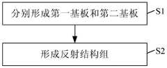
为实现上述目的,本发明还提供了一种显示面板的制备方法,该制备方法包括:In order to achieve the above object, the present invention also provides a preparation method of a display panel, the preparation method comprising:
分别形成第一基板和第二基板;respectively forming a first substrate and a second substrate;
形成反射结构组,所述反射结构组位于所述第一基板朝向所述第二基板的一侧或背向所述第二基板的一侧,所述反射结构组包括与可视视场一一对应的若干个反射结构,所述反射结构的反射面朝向所述第二基板,所述反射结构用于将以沿预定方向从所述第二基板入射的光线进行反射且反射至对应的可视视场。A reflective structure group is formed, the reflective structure group is located on the side of the first substrate facing the second substrate or the side facing away from the second substrate, the reflective structure group includes a visual field of view one by one A plurality of corresponding reflective structures, the reflective surfaces of the reflective structures face the second substrate, and the reflective structures are used to reflect the light incident from the second substrate in a predetermined direction to a corresponding visible light field of view.
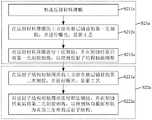
可选地,所述形成反射结构组的步骤包括:Optionally, the step of forming a reflective structure group includes:
依次形成所述反射结构组中的各所述反射结构,所述反射结构包括:沿第一方向设置的若干个反射子结构,位于同一反射结构中的各所述反射子结构的反射面平行设置。Each of the reflection structures in the reflection structure group is sequentially formed, the reflection structure includes: a plurality of reflection substructures arranged along the first direction, and the reflection surfaces of the reflection substructures located in the same reflection structure are arranged in parallel .
可选地,所述形成所述反射结构组中的各反射结构的步骤包括:Optionally, the step of forming each reflective structure in the reflective structure group includes:
通过第一次构图工艺形成与待形成的反射子结构相对应的反射子结构初始图形,所述反射子结构初始图形的纵向截面形状为矩形;An initial pattern of the reflection substructure corresponding to the reflection substructure to be formed is formed by the first patterning process, and the longitudinal cross-sectional shape of the initial pattern of the reflection substructure is a rectangle;
通过第二次构图工艺对所述反射子结构初始图形进行斜面刻蚀,以形成纵向截面形状为直角三角形的反射子结构。The initial pattern of the reflective substructure is subjected to bevel etching through a second patterning process to form a reflective substructure whose longitudinal cross-sectional shape is a right-angled triangle.
可选地,所述通过第一次构图工艺形成与待形成的反射子结构相对应的反射子结构初始图形形成所述反射子结构初始图形的步骤具体包括:Optionally, the step of forming the initial pattern of the reflective substructure by forming the initial pattern of the reflective substructure corresponding to the reflective substructure to be formed by the first patterning process specifically includes:
形成反射材料薄膜;forming a thin film of reflective material;
在反射材料薄膜的上方涂布整层的第一光刻胶,并进行曝光、显影工艺,位于垂直面刻蚀预留区域的光刻胶去除,位于反射子结构形成区域和斜面刻蚀预留区域的第一光刻胶保留,所述垂直面刻蚀预留区域为在第一方向上与所述反射子结构的垂直面底部的距离小于等于第一预定距离的所有点的集合,所述反射子结构形成区域为后续形成有反射子结构的区域,所述斜面刻蚀预留区域为在第一方向上与所述反射子结构的斜面底部的距离小于等于第二预定距离的所有点的集合;Coat the entire layer of first photoresist on the top of the reflective material film, and perform exposure and development processes. The photoresist located in the vertical surface etching reserved area is removed, and the photoresist located in the reflective substructure forming area and the slope etching reserved area is removed. The first photoresist in the area is reserved, and the reserved area for vertical plane etching is a collection of all points whose distances in the first direction from the bottom of the vertical plane of the reflective substructure are less than or equal to a first predetermined distance, and the The reflective substructure forming area is the area where the reflective substructure is subsequently formed, and the reserved area for bevel etching is all points whose distance from the bottom of the bevel of the reflective substructure in the first direction is less than or equal to the second predetermined distance. gather;
对所述反射材料薄膜进行干法刻蚀,并在刻蚀结束后将第一光刻胶剥离,以得到反射子结构初始图形,所述反射子结构初始图形的纵向截面形状为矩形。Dry etching is performed on the reflective material film, and after the etching is completed, the first photoresist is peeled off to obtain an initial pattern of the reflective substructure, and the longitudinal cross-sectional shape of the initial pattern of the reflective substructure is a rectangle.
可选地,所述通过第二次构图工艺对所述反射子结构初始图形进行斜面刻蚀,以形成纵向截面形状为直角三角形的反射子结构对反射子结构初始图形进行斜面刻蚀的步骤具体包括:Optionally, the step of performing bevel etching on the initial pattern of the reflective substructure by the second patterning process to form a reflective substructure whose longitudinal cross-sectional shape is a right-angled triangle is specific to the step of performing bevel etching on the initial pattern of the reflective substructure. include:
在反射子结构初始图形的上方涂布整层铺设的第二光刻胶,并进行曝光、显影工艺,位于所述斜面刻蚀预留区域的光刻胶去除,位于反射子结构形成区域和垂直面刻蚀预留区域的第二光刻胶保留;Coat the whole layer of second photoresist above the initial pattern of the reflective substructure, and perform exposure and development processes. The photoresist located in the reserved area for the slope etching is removed, and the photoresist located in the formation area of the reflective substructure and the vertical The second photoresist in the reserved area for surface etching remains;
对所述反射子结构初始图形进行湿法刻蚀,并在刻蚀结束后将第二光刻胶剥离,以得到纵向截面形状为直角三角形的反射子结构。Wet etching is performed on the initial pattern of the reflective substructure, and after the etching is completed, the second photoresist is peeled off to obtain a reflective substructure whose longitudinal cross-sectional shape is a right-angled triangle.
可选地,所述形成所述反射结构组中的各反射结构的步骤包括:Optionally, the step of forming each reflective structure in the reflective structure group includes:
形成光敏树脂材料薄膜;forming a photosensitive resin material film;
采用灰阶掩膜板对所述光敏树脂材料薄膜进行曝光,并对曝光后的光敏树脂材料薄膜进行显影处理,以得到与待形成的反射子结构相对应的反射子结构衬底模型,所述反射子结构衬底模型具有一垂直面和一斜面,反射子结构衬底模型的纵向截面形状为直角三角形;The photosensitive resin material film is exposed by a gray-scale mask, and the exposed photosensitive resin material film is developed to obtain a reflective substructure substrate model corresponding to the reflective substructure to be formed. The reflection substructure substrate model has a vertical plane and an inclined plane, and the longitudinal cross-sectional shape of the reflection substructure substrate model is a right triangle;
在所述反射子结构衬底模型的表面形成反射材料薄膜,所述反射子结构衬底模型与覆盖所述反射子结构衬底模型的垂直面和斜面的部分构成所述反射子结构。A reflective material film is formed on the surface of the reflective substructure substrate model, and the reflective substructure substrate model and the part covering the vertical plane and the inclined plane of the reflective substructure substrate model constitute the reflective substructure.
可选地,所述形成反射结构组的步骤包括:Optionally, the step of forming a reflective structure group includes:
形成反射材料薄膜;forming a thin film of reflective material;
对所述反射材料薄膜进行构图,以形成所述反射结构和功能结构,所述功能结构位于相邻的反射结构之间,所述功能结构朝向所述第二基板的一侧为与所述第二基板平行的反射面。The reflective material film is patterned to form the reflective structure and the functional structure, the functional structure is located between adjacent reflective structures, and the side of the functional structure facing the second substrate is the same as the second substrate. The reflecting surfaces of the two substrates are parallel.
可选地,所述反射材料薄膜的材料为金属材料。Optionally, the material of the reflective material film is a metal material.
本发明具有如下有益效果:The present invention has the following beneficial effects:
本发明提供了本发明提供了一种显示面板及其制备方法和显示装置,该显示面板包括:相对设置的第一基板和第二基板,第一基板和第二基板之间设置有液晶层,第一基板朝向第二基板的一侧若干个反射结构组,反射结构组包括与可视视场一一对应的若干个反射结构,反射结构的反射面朝向第二基板;反射结构用于将以沿预定方向从第二基板入射的光线进行反射且反射至对应的可视视场。本发明的技术方案可实现反射型液晶显示面板的多可视视场显示。The present invention provides a display panel, a preparation method thereof, and a display device, the display panel includes: a first substrate and a second substrate arranged oppositely, a liquid crystal layer is arranged between the first substrate and the second substrate, There are several reflective structure groups on the side of the first substrate facing the second substrate, the reflective structure group includes several reflective structures corresponding to the visible field of view, and the reflective surfaces of the reflective structures face the second substrate; the reflective structures are used to The light incident from the second substrate in a predetermined direction is reflected and reflected to a corresponding visible field of view. The technical scheme of the present invention can realize the multi-viewing field display of the reflective liquid crystal display panel.
附图说明Description of drawings
图1为本发明实施例一提供的一种显示面板的结构示意图;FIG. 1 is a schematic structural diagram of a display panel according to Embodiment 1 of the present invention;
图2为本发明中反射结构组的结构示意图;2 is a schematic structural diagram of a reflection structure group in the present invention;
图3为图2所示反射结构组的俯视图;Fig. 3 is the top view of the reflection structure group shown in Fig. 2;
图4为本发明中反射结构的结构示意图;4 is a schematic structural diagram of a reflective structure in the present invention;
图5为本发明提供的显示面板实现多可视视场显示的原理示意图;FIG. 5 is a schematic diagram of the principle of realizing multi-view field display by the display panel provided by the present invention;
图6为显示面板上相邻的视场显示区域的显示画面出现串扰时的示意图;6 is a schematic diagram when crosstalk occurs between display images of adjacent field of view display areas on the display panel;
图7为在相邻反射结构之间设置功能结构的示意图;Fig. 7 is the schematic diagram that the functional structure is arranged between adjacent reflective structures;
图8a为本发明中第一基板上设置有像素电极且像素电极复用为反射结构的示意图;FIG. 8a is a schematic diagram of the present invention, wherein pixel electrodes are disposed on the first substrate and the pixel electrodes are multiplexed into a reflective structure;
图8b为本发明中第一基板上设置有像素电极和公共电极且两者复用为反射结构的示意图;FIG. 8b is a schematic diagram of the present invention, where a pixel electrode and a common electrode are disposed on the first substrate, and the two are multiplexed into a reflective structure;
图9为本发明实施例二提供的一种显示面板的结构示意图;FIG. 9 is a schematic structural diagram of a display panel according to
图10为本发明实施例四提供的一种显示面板的制备方法的流程图。FIG. 10 is a flowchart of a method for manufacturing a display panel according to Embodiment 4 of the present invention.
图11为图10中步骤S2对应的一种制备方法的流程图;Fig. 11 is a flow chart of a preparation method corresponding to step S2 in Fig. 10;
图12为采用图11所示流程图制备反射结构组的生产流程示意图;12 is a schematic diagram of a production process for preparing a reflective structure group using the flow chart shown in FIG. 11;
图13为图10中步骤S2对应的又一种制备方法的流程图;Fig. 13 is a flow chart of another preparation method corresponding to step S2 in Fig. 10;
图14为采用图13所示流程图制备反射结构组的生产流程示意图。FIG. 14 is a schematic diagram of a production process for preparing a reflective structure group using the flow chart shown in FIG. 13 .
具体实施方式Detailed ways
为使本领域的技术人员更好地理解本发明的技术方案,下面结合附图对本发明提供的一种显示面板及其制备方法和显示装置进行详细描述。In order for those skilled in the art to better understand the technical solutions of the present invention, a display panel, a manufacturing method thereof, and a display device provided by the present invention are described in detail below with reference to the accompanying drawings.
需要说明的是,本发明中的显示面板为基于反射原理进行显示的反射型液晶显示面板,即外部光源或自然光提供的平行光从入光侧射入至液晶显示面板内,并在反射层的作用下将光线从入光侧射出,从而使得用户观察到显示画面。It should be noted that the display panel in the present invention is a reflective liquid crystal display panel that displays based on the reflection principle, that is, parallel light provided by an external light source or natural light is incident into the liquid crystal display panel from the light incident side, and is formed on the surface of the reflective layer. Under the action, the light is emitted from the light incident side, so that the user can observe the display screen.
本发明中的“可视视场”是指光线沿预定方向(预先人为设定)指入射直至显示面板内时,用户可正常观察显示面板中的显示画面时对应的区域。其中,该“预定方向”一般可设计为垂直于显示面板的方向(外部光源或太阳正对显示面板,以使得平行光垂直射向显示面板),当然也可以为相对于显示面板倾斜一定角度的方向。在本发明中,入射至显示面板内光线所对应的“预定方向”、“可视视场”的数量以及各“可视视场”相对于显示面板的具体位置,可根据实际需要进行预先设定。The "viewable field of view" in the present invention refers to the area corresponding to when the light enters the display panel along a predetermined direction (pre-set artificially) and the user can normally observe the display screen in the display panel. Wherein, the "predetermined direction" can generally be designed as a direction perpendicular to the display panel (the external light source or the sun is facing the display panel, so that the parallel light is perpendicular to the display panel), of course, it can also be inclined at a certain angle relative to the display panel. direction. In the present invention, the "predetermined direction", the number of "viewable fields of view" corresponding to the light incident on the display panel, and the specific position of each "viewable field of view" relative to the display panel can be preset according to actual needs. Certainly.
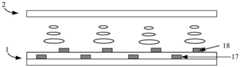
图1为本发明实施例一提供的一种显示面板的结构示意图,图2为本发明中反射结构组的结构示意图,图3为图2所示反射结构组的俯视图,图4为本发明中反射结构的结构示意图,如图1至图4所示,该显示面板对应至少两个可视视场,显示面板包括:相对设置的第一基板1和第二基板2,第一基板1和第二基板2之间设置有液晶层4,第一基板1朝向第二基板2的一侧若干个反射结构组3,反射结构组3包括与可视视场一一对应的若干个反射结构31,反射结构31的反射面朝向第二基板2;反射结构31用于将以沿预定方向从第二基板2入射的光线进行反射且反射至对应的可视视场。1 is a schematic structural diagram of a display panel according to Embodiment 1 of the present invention, FIG. 2 is a schematic structural diagram of a reflective structure group in the present invention, FIG. 3 is a top view of the reflective structure group shown in FIG. Schematic diagrams of the structure of the reflective structure, as shown in FIG. 1 to FIG. 4 , the display panel corresponds to at least two visual fields of view, and the display panel includes: a first substrate 1 and a
可选地,反射结构31的材料为金属材料,例如金属银,由金属银构成的结构的表面可提高较佳的镜面反射效果。Optionally, the material of the
需要说明的是,本实施例中的显示面板为扭曲向列(Twisted Nematic,简称TN)型液晶显示面板、面内转换(In-Plane Switching,简称IPS)型液晶显示面板、边缘场开关(Fringe Field Switching,简称FFS)型液晶显示面板、垂直配向(Vertical Alignment,简称VA)型液晶显示面板、高级超维场转换(Advanced Super Dimension Switch,简称ADS)型液晶显示面板中一种。对于上述各类型液晶显示面板中用于对液晶进行取向的取向层(未示出,取向层与液晶层4接触),以及用于驱动液晶进行偏转的电极(像素电极和公共电极)的具体内容,此处不再赘述。It should be noted that the display panel in this embodiment is a twisted nematic (TN) type liquid crystal display panel, an in-plane switching (referred to as IPS) type liquid crystal display panel, a fringe field switch (Fringe Field Switching (FFS) type liquid crystal display panel, Vertical Alignment (Vertical Alignment, VA) type liquid crystal display panel, Advanced Super Dimension Switch (Advanced Super Dimension Switch, ADS for short) type liquid crystal display panel. The specific content of the alignment layer (not shown, the alignment layer is in contact with the liquid crystal layer 4 ) for aligning the liquid crystal and the electrodes (pixel electrode and common electrode) for driving the liquid crystal to deflect in the above-mentioned various types of liquid crystal display panels , and will not be repeated here.
本实施例中,以第一基板1为阵列基板,第二基板2可为对盒基板为例,进行示例型描述,此时第一基板1上设置有薄膜晶体管阵列,第二基板2上设置有用于进行彩色画面显示的彩膜层(彩色滤光图形阵列);当然,在本发明中也可以是第一基板1为对盒基板,第二基板2为阵列基板。In this embodiment, the first substrate 1 is an array substrate, and the
下面将结合附图来对本发明提供的显示面板实现多可视视场显示的原理进行详细描述。The principle of realizing multi-view field display by the display panel provided by the present invention will be described in detail below with reference to the accompanying drawings.
图5为本发明提供的显示面板实现多可视视场显示的原理示意图,如图5所示,作为本发明中的一种可选方案,显示面板上划分有若干个视场显示区域组,视场显示区域组与反射结构组3一一对应,视场显示区域组中划分有沿第一方向X排列且与可视视场一一对应的若干个视场显示区域,反射结构31与视场显示区域一一对应。FIG. 5 is a schematic diagram of the principle of realizing multi-view field display by the display panel provided by the present invention. As shown in FIG. 5 , as an optional solution in the present invention, the display panel is divided into several field of view display area groups. The field of view display area group is in one-to-one correspondence with the reflection structure group 3. The field of view display area group is divided into several field of view display areas arranged along the first direction X and corresponding to the visible field of view one-to-one. Field display areas are in one-to-one correspondence.
以预定方向为垂直于显示面板的方向为例,假定可视视场的数量为四个为例,分别记为第一可视视场、第二可视视场、第三可视视场、第四可视视场;显示面板上与上述四个可视视场对应的四个视场显示区域分别记为第一视场显示区域、第二视场显示区域、第三视场显示区域、第四可视场显示区域;反射结构组3中与上述四个可视视场对应的四个反射结构31分别记为第一反射结构31a、第二反射结构31b、第三反射结构31c、第四反射结构31d。Taking the predetermined direction as the direction perpendicular to the display panel as an example, it is assumed that the number of visible fields of view is four as an example, which are respectively recorded as the first visible field of view, the second visible field of view, the third visible field of view, The fourth visual field of view; the four visual field display areas on the display panel corresponding to the above four visual fields of view are respectively denoted as the first visual field display area, the second visual field display area, the third visual field display area, The fourth visible field display area; the four
在显示面板上的第一视场显示区域,平行光垂直于显示面板且从第一视场显示区域射入,经过液晶层4作用后,光线到达第一视场显示区域对应的第一反射结构31a的反射面时,第一反射结构31a将该光线进行反射,并使得反射光线从与入射时相同的第一视场显示区域射出,并射向第一可视视场。因此,用户可在可视视场观察到显示面板上第一视场显示区域所呈现的第一显示画面。In the display area of the first field of view on the display panel, parallel light is perpendicular to the display panel and is incident from the display area of the first field of view. After the action of the liquid crystal layer 4, the light reaches the first reflection structure corresponding to the display area of the first field of view When the reflective surface of 31a is used, the first
在显示面板上的第二视场显示区域,平行光垂直于显示面板且从第二视场显示区域射入,经过液晶层4作用后,光线到达第二视场显示区域对应的第二反射结构31b的反射面时,第二反射结构31b将该光线进行反射,并使得反射光线从与入射时相同的第二视场显示区域射出,并射向第二可视视场。因此,用户可在可视视场观察到显示面板上第二视场显示区域所呈现的第二显示画面。In the display area of the second field of view on the display panel, the parallel light is perpendicular to the display panel and is incident from the display area of the second field of view. After the action of the liquid crystal layer 4, the light reaches the second reflection structure corresponding to the display area of the second field of view When the reflective surface of 31b is used, the second
在显示面板上的第三视场显示区域,平行光垂直于显示面板且从第三视场显示区域射入,经过液晶层4作用后,光线到达第三视场显示区域对应的第三反射结构31c的反射面时,第三反射结构31c将该光线进行反射,并使得反射光线从与入射时相同的第三视场显示区域射出,并射向第三可视视场。因此,用户可在可视视场观察到显示面板上第三视场显示区域所呈现的第三显示画面。In the display area of the third field of view on the display panel, the parallel light is perpendicular to the display panel and is incident from the display area of the third field of view. After the action of the liquid crystal layer 4, the light reaches the third reflection structure corresponding to the display area of the third field of view When the reflective surface of 31c is used, the third
在显示面板上的第四视场显示区域,平行光垂直于显示面板且从第四视场显示区域射入,经过液晶层4作用后,光线到达第四视场显示区域对应的第四反射结构31d的反射面时,第四反射结构31d将该光线进行反射,并使得反射光线从与入射时相同的第四视场显示区域射出,并射向第四可视视场。因此,用户可在可视视场观察到显示面板上第四视场显示区域所呈现的第四显示画面。In the display area of the fourth field of view on the display panel, the parallel light is perpendicular to the display panel and is incident from the display area of the fourth field of view. After the action of the liquid crystal layer 4, the light reaches the fourth reflection structure corresponding to the display area of the fourth field of view When the reflective surface of 31d is used, the fourth
由此可见,本发明提供的显示面板可实现多可视视场。当一个用户的两只眼睛分别处于不同可视视场时,即左眼和右眼能分别看到不同显示画面,从而达到裸眼3D的效果。It can be seen that the display panel provided by the present invention can realize multiple viewing fields. When the two eyes of a user are in different visual fields, that is, the left eye and the right eye can see different display images respectively, so as to achieve the naked-eye 3D effect.
需要说明的是,对于各反射结构组3中各反射结构31的反射面的倾斜角度,可根据该反射结构31在显示面板中的位置以及该反射结构31对应的可视视场的位置进行相应设计。位于不同反射结构组3中对应相同可视视场的反射结构31,其反射面的倾斜角度可以不同。It should be noted that, for the inclination angle of the reflective surface of each
此外,上述可视视场为四个、四个可视视场沿第一方向排列的情况仅起到示例性作用,其不会对本发明的技术方案产生限制。在本发明中,可根据需要来对可视视场的数量(例如两个、三个)、位置(例如全部可视视场呈阵列排布)进行相应设计。在实际应用中,当显示面板的物理分辨率一定且各可视视场对应的显示画面分辨率相同时,可视视场的数量越多,各可可视视场对应的显示画面分辨率越低,显示效果越差。为此,本实施例中优选地,显示面板对应的可视视场2~4个,可在实现多可可视视场的同时保证显示质量。In addition, the above-mentioned case where the visible fields of view are four and the four visible fields of view are arranged along the first direction only serves as an example, and does not limit the technical solution of the present invention. In the present invention, the number (eg, two, three) and positions of the visible fields of view (eg, all the visible fields of view are arranged in an array) can be designed correspondingly as required. In practical applications, when the physical resolution of the display panel is constant and the display resolutions corresponding to each visible field of view are the same, the greater the number of visible fields of view, the lower the display resolution corresponding to each visible field of view. , the display effect is worse. For this reason, in this embodiment, preferably, the display panel corresponds to 2-4 visual fields of view, which can ensure the display quality while realizing multiple visual fields of view.
作为本发明的一种优选方案,反射结构31包括:沿第一方向X设置的若干个反射子结构311,位于同一反射结构31中的各反射子结构311的反射面平行设置。当平行光照射至同一反射结构31中的不同反射子结构311的反射面时,不同反射子结构311的反射面处的反射光线会发生增强干涉,从而能提升显示亮度,进而能提升该显示面板在弱光环境下的对比度。可选地,反射子结构311的纵向截面(垂直于显示面板且与第一方向X平行的截面)形状为直角三角形,直角三角形的斜边作为反射面。每个反射结构31中的反射子结构311的数目可以是一个,也可以是多个。As a preferred solution of the present invention, the
图6为显示面板上相邻的视场显示区域的显示画面出现串扰时的示意图,如图6所示,以可视视场的数量为两个为例,分别记为左眼可视视场和右眼第二可视视场;显示面板上与上述两个可视视场对应的视场显示区域为左眼视场显示区域和右眼视场显示区域,其中位于左眼视场显示区域内的像素为左眼像素61,位于右眼视场显示区域内的像素为右眼像素62;反射结构组3中与上述两个可视视场对应的反射结构31分别记为左眼反射结构和右眼反射结构,其中左眼反射结构具有左眼反射面32,右眼反射结构具有右眼反射面33。FIG. 6 is a schematic diagram of the display screen of the adjacent field of view display areas on the display panel when crosstalk occurs. As shown in FIG. 6 , taking the number of visible fields of view as two as an example, it is denoted as the left eye visible field of view respectively. and the second visual field of view of the right eye; the visual field display areas corresponding to the above two visual fields of view on the display panel are the left eye visual field display area and the right eye visual field display area, which are located in the left eye visual field display area The pixels inside are the left-
在进行裸眼3D显示时,以预定方向射入左眼像素61的光线51a,在左眼反射面32发生反射后,反射光线51b再次经过左眼像素61,并射向左眼可视视场,以在用户的左眼形成左眼显示画面;以预定方向射入右眼像素62的光线52a,在右眼反射面33发生反射后,反射光线52b再次经过右眼像素62,并射向右眼可视视场以在用户的右眼形成右眼显示画面。然而,在实际使用过程中,不可避免的存在一些不处于预定角度的环境光射如至显示面板中,以图中环境光线53a为例,环境光线53a以非预定角度射入右眼像素62,并在左眼反射面32发生反射,且反射光线53b再次经过右眼像素62射向用户的左眼,此时出现画面串扰。When performing naked-eye 3D display, the
为解决上述技术问题,本发明在相邻的反射结构31之间设置一功能结构35,该功能结构35朝向第二基板2的一侧为与第二基板2平行的功能面,功能面为反射面或吸光面,从而能有效解决画面串扰的问题。图7为在相邻反射结构之间设置功能结构的示意图,如图7所示,以功能结构35中的功能面为反射面为例,图6中产生画面串扰的环境光线53a经过右眼像素后射向功能面34,并在在功能结构35上的功能面34发生反射,反射光线53b射向左眼像素。在彩色显示面板中,由于左眼像素和右眼像素的彩膜颜色(彩色滤光图形)不同,因此反射光线53b不能透过显示面板,从而有效防止左眼显示画面和右眼显示画面发生串扰。In order to solve the above-mentioned technical problems, the present invention provides a
当功能结构35中的功能面34为吸光面时,环境光线53a经过右眼像素后射向功能面,功能面34将光线53a吸收,从而有效防止左眼显示画面和右眼显示画面发生串扰。When the
在本实施例中,当功能结构35功能面为反射面时,功能结构35与反射结构31一体成型,即功能结构35和反射结构31可通过一次构图进行制备,具体制备过程可参见后续内容。In this embodiment, when the functional surface of the
需要说明的是,上述可视视场包括左眼可视视场和右眼可视视场,功能结构35以防止左眼显示画面和右眼显示画面发生串扰的情况仅起到示例性作用。本领域技术人员应该知晓的是,当可视视场数量为多个时,通过在相邻反射结构31之间设置功能结构35,可有效防止任意相邻两个可视视场对应的显示画面出现串扰。It should be noted that the above-mentioned visible field of view includes a left-eye viewable field and a right-eye viewable field, and the
在本实施例,作为一种优选方案,当第一基板上设置有像素电极和/或公共电极时,可使得位于第一基板上的像素电极和/或公共电极采用金属材料进行制备,并将该像素电极和/或公共电极复用作反射结构。In this embodiment, as a preferred solution, when pixel electrodes and/or common electrodes are provided on the first substrate, the pixel electrodes and/or common electrodes on the first substrate can be prepared with metal materials, and the The pixel electrodes and/or the common electrodes are multiplexed as reflective structures.
图8a为本发明中第一基板上设置有像素电极且像素电极复用为反射结构的示意图,如图8a所示,作为一种可选方案,第一基板1上设置有像素电极17,第二基板2上设置有公共电极18,像素电极17与公共电极18之间产生垂直电场控制液晶偏转,公共电极18由透明材料制成,像素电极17由金属材料制成,该像素电极17可复用为反射结构。FIG. 8a is a schematic diagram of the present invention where pixel electrodes are provided on the first substrate and the pixel electrodes are multiplexed into a reflective structure. As shown in FIG. 8a, as an optional solution, pixel electrodes 17 are provided on the first substrate 1, and the first substrate 1 is provided with a pixel electrode 17. The two
当然,也可以是将像素电极17设置于第二基板2上,像素电极17由透明材料制成,将公共电极18设置于第一基板上,公共电极18由金属材料制成,该公共电极18可复用为反射结构。Of course, the pixel electrode 17 can also be disposed on the
图8b为本发明中第一基板上设置有像素电极和公共电极且两者复用为反射结构的示意图,如图8b所示,作为又一种可选方案,像素电极17和公共电极18均位于第一基板上,像素电极17与公共电极18之间产生边缘电场以控制液晶偏转,像素电极17和公共电极18均采用金属材料制成,两者均复用为反射结构。FIG. 8b is a schematic diagram of the present invention where a pixel electrode and a common electrode are disposed on the first substrate, and the two are multiplexed into a reflective structure. As shown in FIG. 8b, as another alternative, the pixel electrode 17 and the
通过上述内容可见,通过将公共电极18和/或像素电极17复用为反射结构,因而无需额外设计膜层来形成反射结构,有效减小显示面板的厚度,有利于显示面板的轻薄化。当然,通过在第一基板1朝向第二基板2的一侧额外设计膜层来形成反射结构的情况,其也属于本发明的保护范围,本实施例中对反射结构所处位置不作限定,仅需保证反射结构能对穿过液晶层的光线进行反射即可。It can be seen from the above content that by multiplexing the
图9为本发明实施例二提供的一种显示面板的结构示意图,如图9所示,与上述实施例一种不同的是,本发明中的反射结构组3位于第一基板1背向第二基板2的一侧。对于本实施例中利用反射结构组3实现多可视视场显示的具体过程,此处不再赘述。FIG. 9 is a schematic structural diagram of a display panel according to the second embodiment of the present invention. As shown in FIG. 9 , different from the above-mentioned first embodiment, the reflective structure group 3 in the present invention is located on the first substrate 1 away from the second Two sides of the
本发明实施例三提供了一种显示装置,该显示装置包括显示面板,该显示面板采用上述实施例一或实施例二中的显示面板,对于该显示面板的描述可参见前述实施例一和实施例二中的内容,此处不再赘述。Embodiment 3 of the present invention provides a display device, the display device includes a display panel, and the display panel adopts the display panel in the first embodiment or the second embodiment. For the description of the display panel, please refer to the foregoing embodiment 1 and implementation The content in Example 2 will not be repeated here.
本发明实施例四提供了一种显示面板的制备方法,用于制备上述实施例一和实施例二中提供的显示面板。图10为本发明实施例四提供的一种显示面板的制备方法的流程图,如图10所示,该显示面板的制备方法包括:Embodiment 4 of the present invention provides a method for manufacturing a display panel, which is used to manufacture the display panels provided in Embodiment 1 and
步骤S1、分别形成第一基板和第二基板。Step S1, respectively forming a first substrate and a second substrate.
第一基板和第二基板中的一者为阵列基板,另一者为对盒基板。通过现有的阵列基板制备工艺和对盒基板基板,以制备第一基板和第二基板。One of the first substrate and the second substrate is an array substrate, and the other is a cell assembly substrate. The first substrate and the second substrate are prepared by using the existing array substrate preparation process and cell assembly substrates.
步骤S2、形成反射结构组。Step S2, forming a reflection structure group.
反射结构组包括与可视视场一一对应的若干个反射结构,反射结构的反射面朝向第二基板,反射结构用于将以沿预定方向从第二基板入射的光线进行反射且反射至对应的可视视场。The reflective structure group includes a number of reflective structures corresponding to the visible field of view, the reflective surface of the reflective structures faces the second substrate, and the reflective structures are used to reflect the light incident from the second substrate in a predetermined direction and reflect it to the corresponding visual field of view.
图11为图10中步骤S2对应的一种制备方法的流程图,图12为采用图11所示流程图制备反射结构组的生产流程示意图,如图11和图12所示,当反射结构包括沿第一方向设置的若干个反射子结构,且反射子结构的纵向截面形状为直角三角形时,作为本实施例中的一种可选方案,步骤S2包括:依次形成反射结构组中的各反射结构。反射结构包括:沿第一方向设置的若干个反射子结构,位于同一反射结构中的各反射子结构的反射面平行设置。11 is a flowchart of a preparation method corresponding to step S2 in FIG. 10 , and FIG. 12 is a schematic diagram of a production process of preparing a reflective structure group using the flowchart shown in FIG. 11 . As shown in FIGS. 11 and 12 , when the reflective structure includes When several reflective substructures are arranged along the first direction, and the longitudinal cross-sectional shape of the reflective substructure is a right-angled triangle, as an optional solution in this embodiment, step S2 includes: sequentially forming each reflection in the reflective structure group structure. The reflection structure includes: a plurality of reflection substructures arranged along the first direction, and the reflection surfaces of the reflection substructures located in the same reflection structure are arranged in parallel.
形成反射结构的步骤包括:The steps of forming the reflective structure include:
步骤S21a、通过第一次构图工艺形成与待形成的反射子结构相对应的反射子结构初始图形,反射子结构初始图形的纵向截面形状为矩形。Step S21a, an initial pattern of the reflection substructure corresponding to the reflection substructure to be formed is formed through the first patterning process, and the longitudinal cross-sectional shape of the initial pattern of the reflection substructure is a rectangle.
步骤S21a具体包括:Step S21a specifically includes:
步骤S211a、形成反射材料薄膜。Step S211a, forming a reflective material film.
在步骤S211a中,通过蒸镀或气相沉积工艺在衬底7上形成反射材料薄膜8。可选地,反射材料薄膜8的材料为金属材料。In step S211a, a reflective material thin film 8 is formed on the
步骤S212a、在反射材料薄膜的上方涂布整层铺设的第一光刻胶,并进行曝光、显影工艺。Step S212a, coating the entire layer of the first photoresist on the top of the reflective material film, and performing exposure and development processes.
由于反射子结构的纵向截面形状为直角三角形,则最终成型的反射子结构必然包括一与显示面板垂直的垂直面以及一相对于显示面板倾斜一定角度的斜面。Since the longitudinal cross-sectional shape of the reflective substructure is a right triangle, the final formed reflective substructure must include a vertical plane perpendicular to the display panel and an inclined plane inclined at a certain angle relative to the display panel.
在本发明中,针对各反射子结构,可预先设计出对应的反射子结构形成区域12、垂直面刻蚀预留区域10、斜面刻蚀预留区域11。其中,反射子结构形成区域12为后续形成有反射子结构的区域,垂直面刻蚀预留区域10为在第一方向X上与反射子结构的垂直面底部的距离小于等于第一预定距离a的所有点的集合,斜面刻蚀预留区域11为在第一方向上与反射子结构的斜面底部的距离小于等于第二预定距离b的所有点的集合。In the present invention, for each reflective substructure, a corresponding reflective
其中,第一预定距离a和第二预定距离b可以根据实际需要进行设计和调整。The first predetermined distance a and the second predetermined distance b can be designed and adjusted according to actual needs.
经过步骤S212a处理后,位于垂直面刻蚀预留区域10的第一光刻胶9去除,位于反射子结构形成区域12和斜面刻蚀预留区域11的第一光刻胶9保留。After the step S212a, the
步骤S213a、对反射材料薄膜进行干法刻蚀,并在刻蚀结束后将第一光刻胶剥离,以得到反射子结构初始图形。In step S213a, dry etching is performed on the reflective material film, and after the etching is completed, the first photoresist is peeled off to obtain an initial pattern of the reflective substructure.
由于干法刻蚀工艺仅对相应的膜层在垂直方向Y上进行刻蚀,因此经干法刻蚀形成的反射子结构初始图形81的侧面必然与显示面板垂直(反射子结构初始图形81的纵向截面为矩形),此时可反射子结构初始图形81的一个侧面可作为最终成型的反射子结构的垂直面。Since the dry etching process only etches the corresponding film layer in the vertical direction Y, the side surface of the
需要说明的是,在本实施例中,可采用一次构图工艺以同时制备出显示面板上各反射结构中的反射子结构初始图形,以缩短生产周期。It should be noted that, in this embodiment, a patterning process can be used to simultaneously prepare the initial patterns of the reflective substructures in each reflective structure on the display panel, so as to shorten the production cycle.
步骤S22a、通过第二次构图工艺对反射子结构初始图形进行斜面刻蚀,以形成纵向截面形状为直角三角形的反射子结构。Step S22a, performing bevel etching on the initial pattern of the reflective sub-structure through a second patterning process to form a reflective sub-structure whose longitudinal cross-sectional shape is a right-angled triangle.
步骤S22a具体包括:Step S22a specifically includes:
步骤S221a、在反射子结构初始图形的上方涂布整层铺设的第二光刻胶,并进行曝光、显影工艺。In step S221a, a whole layer of second photoresist is applied over the initial pattern of the reflective substructure, and exposure and development processes are performed.
经过步骤S221a处理后,位于斜面刻蚀预留区域11的第二光刻胶13去除,位于反射子结构形成区域12和垂直面刻蚀预留区域10的第二光刻胶13保留。After the step S221a, the
其中,位于垂直面刻蚀预留区域10的第二光刻胶13完全覆盖最终成型的反射子结构的垂直面(反射子结构初始图形81的一个侧面),以避免该垂直面在后续湿法刻蚀中被误刻蚀。Wherein, the
步骤S222a、对反射子结构初始图形进行湿法刻蚀,并在刻蚀结束后将第二光刻胶剥离,以得到纵向截面形状为直角三角形的反射子结构。In step S222a, wet etching is performed on the initial pattern of the reflective sub-structure, and after the etching is completed, the second photoresist is peeled off to obtain a reflective sub-structure whose longitudinal cross-sectional shape is a right-angled triangle.
在进行湿法刻蚀时,刻蚀液不仅能在垂直方向Y上进行刻蚀,还能在水平方向(第一方向X)上进行刻蚀,通过对工艺参数、反应时间等因子进行控制,最终可到具有一定倾斜角的斜面。During wet etching, the etching solution can not only etch in the vertical direction Y, but also etch in the horizontal direction (the first direction X). By controlling the process parameters, reaction time and other factors, Finally, a slope with a certain inclination angle can be reached.
由上述内容可见,通过干法刻蚀可得到反射子结构311的垂直面,通过湿法刻蚀可得到反射子结构311的斜面,且能对斜面的倾斜角进行控制。It can be seen from the above content that the vertical surface of the
在步骤S22a中,通过一次斜面刻蚀工艺(步骤S221a和步骤S222a),仅能得到具有某一特定倾斜角的斜面。对应于不同倾斜角的斜面,需要进行多次斜面刻蚀工艺。在进行某一次斜面刻蚀工艺中,对于暂不需要进行刻蚀的反射子结构初始图形以及已经成型的反射子结构均需使用光刻胶进行覆盖、保护,以避免出现误刻蚀。In step S22a, only a slope with a certain slope angle can be obtained through one slope etching process (step S221a and step S222a). Corresponding to the bevels with different inclination angles, multiple bevel etching processes are required. In a certain slope etching process, the initial pattern of the reflective substructure that does not need to be etched temporarily and the formed reflective substructure need to be covered and protected with photoresist to avoid mis-etching.
需要说明的是,当反射结构之间形成有功能结构且功能结构的表面为反射面时,可对步骤S212a中显影后保留的第一光刻胶的区域进行调整,以使得位于待形成功能结构的区域的第一光刻胶保留,经过步骤S213a的干法刻蚀后,可同时得到功能结构的图形。It should be noted that, when a functional structure is formed between the reflective structures and the surface of the functional structure is a reflective surface, the area of the first photoresist remaining after the development in step S212a can be adjusted so as to be located in the functional structure to be formed The first photoresist in the area of is retained, and after the dry etching in step S213a, the pattern of the functional structure can be obtained at the same time.
图13为图10中步骤S2对应的又一种制备方法的流程图,图14为采用图13所示流程图制备反射结构组的生产流程示意图,如图13和图14所示,作为本实施例中的又一种制备纵向截面形状为直角三角形的反射子结构的可选方案,步骤S2包括:FIG. 13 is a flowchart of another preparation method corresponding to step S2 in FIG. 10 , and FIG. 14 is a schematic diagram of the production process of preparing a reflective structure group using the flowchart shown in FIG. 13 , as shown in FIGS. 13 and 14 , as the embodiment Another optional scheme for preparing a reflective substructure whose longitudinal cross-sectional shape is a right-angled triangle in the example, step S2 includes:
步骤S21b、形成光敏树脂材料薄膜。Step S21b, forming a photosensitive resin material film.
在步骤S21b中,在衬底7上涂布一层光敏树脂材料薄膜14。In step S21b, a layer of photosensitive
步骤S22b、采用灰阶掩膜板对光敏树脂材料薄膜进行曝光,并对曝光后的光敏树脂材料薄膜进行显影处理,以得到与待形成的反射子结构相对应的反射子结构衬底模型,反射子结构衬底模型具有一垂直面和一斜面,反射子结构衬底模型的纵向截面形状为直角三角形。In step S22b, the photosensitive resin material film is exposed by using a gray-scale mask, and the exposed photosensitive resin material film is developed to obtain a reflective substructure substrate model corresponding to the reflective substructure to be formed. The substructure substrate model has a vertical plane and an inclined plane, and the longitudinal section shape of the reflection substructure substrate model is a right triangle.
在步骤S22b中,通过灰阶掩膜板对光敏树脂材料薄膜14进行曝光,灰阶掩膜板上具有透光率不同的透光区域,以对光敏树脂材料薄膜上不同区域进行不同程度的曝光。经过显影处理后,可得到截面形状为直角三角形的若干个反射子结构衬底模型15。反射子结构衬底模型15的斜面倾斜角与其对应的反射子结构的斜面倾斜角相同。In step S22b, the photosensitive
步骤S23b、在反射子结构衬底模型的表面形成反射材料薄膜,反射子结构衬底模型与覆盖反射子结构衬底模型的垂直面和斜面的部分构成反射子结构。Step S23b, a reflective material film is formed on the surface of the reflective sub-structure substrate model, and the reflective sub-structure substrate model and the part covering the vertical plane and the inclined plane of the reflective sub-structure substrate model constitute a reflective sub-structure.
在步骤S23b中,在步骤S22b所得到的基板的表面形成一层均匀的反射材料薄膜16,可选地,反射材料薄膜16的材料为金属材料。反射子结构衬底模型15与反射材料薄膜16覆盖该反射子结构衬底模型15的垂直面和斜面的部分构成反射子结构311。由于反射子结构衬底模型15的纵向截面形状为直角三角形,则反射子结构311的纵向截面形状也为直角三角形。In step S23b, a uniform layer of
需要说明的是,当反射结构之间形成有功能结构且功能结构的表面为反射面时,可在步骤S22b中使得对应待形成功能结构的区域的光敏树脂材料完全保留以作为功能结构衬底模型,经过步骤S23b后,功能结构衬底模型与位于其上表面的反射材料薄膜的部分构成功能结构。It should be noted that, when a functional structure is formed between the reflective structures and the surface of the functional structure is a reflective surface, the photosensitive resin material corresponding to the area where the functional structure is to be formed can be completely reserved in step S22b as the functional structure substrate model. , after step S23b, the functional structure substrate model and the part of the reflective material thin film located on the upper surface of the functional structure substrate model constitute a functional structure.
在本实施例中,当反射结构位于第一基板朝向第二基板的一侧时,可以以第一基板作为衬底来形成反射结构组;当反射结构位于第一基板背向第二基板的一侧时,需先在其他衬底上先制备出反射结构组,然后将反射结构组置于第一基板背向第二基板的一侧,且反射结构组中各反射结构的反射面朝向第二基板。In this embodiment, when the reflective structure is located on the side of the first substrate facing the second substrate, the first substrate can be used as a substrate to form a reflective structure group; when the reflective structure is located on a side of the first substrate facing away from the second substrate When the reflective structure group is placed on the other substrate, the reflective structure group should be placed on the side of the first substrate facing away from the second substrate, and the reflective surface of each reflective structure in the reflective structure group should face the second substrate. substrate.
可以理解的是,以上实施方式仅仅是为了说明本发明的原理而采用的示例性实施方式,然而本发明并不局限于此。对于本领域内的普通技术人员而言,在不脱离本发明的精神和实质的情况下,可以做出各种变型和改进,这些变型和改进也视为本发明的保护范围。It can be understood that the above embodiments are only exemplary embodiments adopted to illustrate the principle of the present invention, but the present invention is not limited thereto. For those skilled in the art, without departing from the spirit and essence of the present invention, various modifications and improvements can be made, and these modifications and improvements are also regarded as the protection scope of the present invention.
Claims (11)
Translated fromChinesePriority Applications (4)
| Application Number | Priority Date | Filing Date | Title |
|---|---|---|---|
| CN201710790365.2ACN109426026B (en) | 2017-09-05 | 2017-09-05 | Display panel, preparation method thereof and display device |
| US16/332,168US11327359B2 (en) | 2017-09-05 | 2018-06-29 | Display panel, method for manufacturing the same and display device |
| EP18853270.9AEP3680707B1 (en) | 2017-09-05 | 2018-06-29 | Display panel and preparation method therefor and display device thereof |
| PCT/CN2018/093688WO2019047601A1 (en) | 2017-09-05 | 2018-06-29 | Display panel and preparation method therefor and display device thereof |
Applications Claiming Priority (1)
| Application Number | Priority Date | Filing Date | Title |
|---|---|---|---|
| CN201710790365.2ACN109426026B (en) | 2017-09-05 | 2017-09-05 | Display panel, preparation method thereof and display device |
Publications (2)
| Publication Number | Publication Date |
|---|---|
| CN109426026A CN109426026A (en) | 2019-03-05 |
| CN109426026Btrue CN109426026B (en) | 2022-08-23 |
Family
ID=65513425
Family Applications (1)
| Application Number | Title | Priority Date | Filing Date |
|---|---|---|---|
| CN201710790365.2AActiveCN109426026B (en) | 2017-09-05 | 2017-09-05 | Display panel, preparation method thereof and display device |
Country Status (4)
| Country | Link |
|---|---|
| US (1) | US11327359B2 (en) |
| EP (1) | EP3680707B1 (en) |
| CN (1) | CN109426026B (en) |
| WO (1) | WO2019047601A1 (en) |
Families Citing this family (2)
| Publication number | Priority date | Publication date | Assignee | Title |
|---|---|---|---|---|
| CN114647025B (en)* | 2020-12-21 | 2025-02-28 | 京东方科技集团股份有限公司 | Aerial imaging device, reflector and preparation method thereof |
| CN116931306B (en)* | 2023-07-18 | 2025-08-08 | 惠科股份有限公司 | Display panel and display device |
Citations (3)
| Publication number | Priority date | Publication date | Assignee | Title |
|---|---|---|---|---|
| US6291146B1 (en)* | 1999-04-09 | 2001-09-18 | Industrial Technology Research Institute | Method for reforming a reflection-type light diffuser |
| US6573959B1 (en)* | 1999-04-24 | 2003-06-03 | Sharp Kabushiki Kaisha | Optical element, a method of making a display device and a display device comprising an optical element |
| CN102830537A (en)* | 2012-08-31 | 2012-12-19 | 北京京东方光电科技有限公司 | Color film substrate, manufacturing method thereof and display device |
Family Cites Families (12)
| Publication number | Priority date | Publication date | Assignee | Title |
|---|---|---|---|---|
| CN1311873A (en)* | 1998-07-29 | 2001-09-05 | 松下电器产业株式会社 | Scattering display and method for driving same |
| TW594218B (en)* | 2000-07-03 | 2004-06-21 | Alps Electric Co Ltd | Reflector and reflective liquid crystal display device |
| JP3960085B2 (en)* | 2002-03-06 | 2007-08-15 | セイコーエプソン株式会社 | Stereoscopic image display device |
| JP2005135899A (en)* | 2003-10-06 | 2005-05-26 | Omron Corp | Surface light source apparatus and display apparatus |
| JP4476137B2 (en)* | 2005-02-28 | 2010-06-09 | セイコーエプソン株式会社 | Liquid crystal device and electronic device |
| KR20080086118A (en)* | 2007-03-21 | 2008-09-25 | 엘지디스플레이 주식회사 | Semi-transmissive liquid crystal display device and manufacturing method |
| CN101738760B (en)* | 2008-11-11 | 2012-08-08 | 宏碁股份有限公司 | Pixel structure, optical element, liquid crystal display device and manufacturing method thereof |
| JP2011222237A (en) | 2010-04-07 | 2011-11-04 | Sony Corp | Lighting system and display device |
| CN103185293B (en)* | 2011-12-29 | 2015-03-18 | 上海天马微电子有限公司 | Reflecting plate and total reflection 3D display device |
| CN103454807B (en) | 2013-09-02 | 2016-07-27 | 京东方科技集团股份有限公司 | Array base palte and preparation method thereof, 3D display device |
| CN105372824B (en)* | 2015-12-22 | 2017-12-29 | 苏州苏大维格光电科技股份有限公司 | A kind of bore hole 3D laser display apparatus |
| CN106937106A (en) | 2017-04-07 | 2017-07-07 | 京东方科技集团股份有限公司 | Reflective 3D display devices |
- 2017
- 2017-09-05CNCN201710790365.2Apatent/CN109426026B/enactiveActive
- 2018
- 2018-06-29EPEP18853270.9Apatent/EP3680707B1/enactiveActive
- 2018-06-29USUS16/332,168patent/US11327359B2/enactiveActive
- 2018-06-29WOPCT/CN2018/093688patent/WO2019047601A1/ennot_activeCeased
Patent Citations (3)
| Publication number | Priority date | Publication date | Assignee | Title |
|---|---|---|---|---|
| US6291146B1 (en)* | 1999-04-09 | 2001-09-18 | Industrial Technology Research Institute | Method for reforming a reflection-type light diffuser |
| US6573959B1 (en)* | 1999-04-24 | 2003-06-03 | Sharp Kabushiki Kaisha | Optical element, a method of making a display device and a display device comprising an optical element |
| CN102830537A (en)* | 2012-08-31 | 2012-12-19 | 北京京东方光电科技有限公司 | Color film substrate, manufacturing method thereof and display device |
Also Published As
| Publication number | Publication date |
|---|---|
| WO2019047601A1 (en) | 2019-03-14 |
| CN109426026A (en) | 2019-03-05 |
| US20210349347A1 (en) | 2021-11-11 |
| EP3680707A1 (en) | 2020-07-15 |
| US11327359B2 (en) | 2022-05-10 |
| EP3680707A4 (en) | 2021-06-09 |
| EP3680707B1 (en) | 2024-03-06 |
Similar Documents
| Publication | Publication Date | Title |
|---|---|---|
| CN103454807B (en) | Array base palte and preparation method thereof, 3D display device | |
| US9103989B2 (en) | Method of manufacturing phase difference plate and 3D display panel | |
| CN101162311B (en) | Stereo liquid crystal display device and method for making the same | |
| EP2530942A1 (en) | 3D display panel and method of manufacturing a phase difference plate | |
| CN102707528B (en) | Array base palte and preparation method thereof, display panels and method of work thereof | |
| CN103941469B (en) | Display panel, manufacturing method thereof, and display device | |
| WO2015070585A1 (en) | Liquid crystal prism and manufacturing method thereof, and display apparatus | |
| CN107678167A (en) | 3 d display and display device | |
| KR101298025B1 (en) | Method of manufacturing a lenticular stereoscopic image display device. | |
| WO2017202162A1 (en) | Virtual curved surface display panel, manufacturing method therefor and display device | |
| TWM396974U (en) | Displaying apparatus for switching displaying modes | |
| TWI424197B (en) | Touch panel for displaying stereoscopic image | |
| WO2015018157A1 (en) | Array substrate, colour film substrate, display device and manufacturing method for alignment layer | |
| CN109426026B (en) | Display panel, preparation method thereof and display device | |
| KR101773691B1 (en) | 3D Panel, Manufacturing Method Thereof and 3D Display Device Therewith | |
| CN107678204A (en) | A kind of preparation method of liquid crystal display panel, display and display panel | |
| CN103402111B (en) | Big-sized 2D-3D switching display device | |
| CN106291957A (en) | A kind of parallax baffle, display device and manufacture method thereof | |
| CN205428387U (en) | Display device | |
| CN109148365A (en) | A kind of production method of display panel, display panel and display device | |
| KR20110093508A (en) | Stereoscopic Display and Manufacturing Method Thereof | |
| WO2014173000A1 (en) | Touchscreen capable of implementing 3d display, display apparatus, and method of fabricating touchscreen | |
| KR101971047B1 (en) | Display Device Including Retarder Panel And Method Of Fabricating The Same | |
| KR101966726B1 (en) | Image display device | |
| CN117452663A (en) | Display panel and display device |
Legal Events
| Date | Code | Title | Description |
|---|---|---|---|
| PB01 | Publication | ||
| PB01 | Publication | ||
| SE01 | Entry into force of request for substantive examination | ||
| SE01 | Entry into force of request for substantive examination | ||
| GR01 | Patent grant | ||
| GR01 | Patent grant |