CN109411539B - Semiconductor device, method of manufacturing the same, and electronic apparatus including the same - Google Patents
Semiconductor device, method of manufacturing the same, and electronic apparatus including the sameDownload PDFInfo
- Publication number
- CN109411539B CN109411539BCN201811264731.1ACN201811264731ACN109411539BCN 109411539 BCN109411539 BCN 109411539BCN 201811264731 ACN201811264731 ACN 201811264731ACN 109411539 BCN109411539 BCN 109411539B
- Authority
- CN
- China
- Prior art keywords
- semiconductor
- layer
- sidewall
- nanostructure
- substrate
- Prior art date
- Legal status (The legal status is an assumption and is not a legal conclusion. Google has not performed a legal analysis and makes no representation as to the accuracy of the status listed.)
- Active
Links
- 239000004065semiconductorSubstances0.000titleclaimsabstractdescription165
- 238000004519manufacturing processMethods0.000titleclaimsabstractdescription9
- 239000002086nanomaterialSubstances0.000claimsabstractdescription96
- 239000000758substrateSubstances0.000claimsabstractdescription61
- 239000002070nanowireSubstances0.000claimsdescription55
- 239000000463materialSubstances0.000claimsdescription27
- 238000000034methodMethods0.000claimsdescription19
- 238000005530etchingMethods0.000claimsdescription16
- 238000000059patterningMethods0.000claimsdescription7
- 238000002955isolationMethods0.000claimsdescription3
- 238000013459approachMethods0.000claimsdescription2
- 238000013473artificial intelligenceMethods0.000claimsdescription2
- 239000002064nanoplateletSubstances0.000claims2
- 239000010410layerSubstances0.000description201
- 125000006850spacer groupChemical group0.000description31
- 229920002120photoresistant polymerPolymers0.000description23
- 238000001020plasma etchingMethods0.000description17
- 239000012535impuritySubstances0.000description8
- 239000004020conductorSubstances0.000description7
- 239000002135nanosheetSubstances0.000description5
- 239000011241protective layerSubstances0.000description5
- 238000000206photolithographyMethods0.000description4
- 238000012545processingMethods0.000description4
- 229910000577Silicon-germaniumInorganic materials0.000description3
- 229910052785arsenicInorganic materials0.000description3
- 230000009286beneficial effectEffects0.000description3
- 238000000151depositionMethods0.000description3
- 230000008021depositionEffects0.000description3
- 229910052698phosphorusInorganic materials0.000description3
- 230000003213activating effectEffects0.000description2
- 238000000137annealingMethods0.000description2
- 230000015572biosynthetic processEffects0.000description2
- 238000010586diagramMethods0.000description2
- 238000000407epitaxyMethods0.000description2
- 238000011065in-situ storageMethods0.000description2
- 238000012986modificationMethods0.000description2
- 230000004048modificationEffects0.000description2
- 150000004767nitridesChemical class0.000description2
- 230000003071parasitic effectEffects0.000description2
- 238000006467substitution reactionMethods0.000description2
- 239000000725suspensionSubstances0.000description2
- ZOXJGFHDIHLPTG-UHFFFAOYSA-NBoronChemical compound[B]ZOXJGFHDIHLPTG-UHFFFAOYSA-N0.000description1
- OAICVXFJPJFONN-UHFFFAOYSA-NPhosphorusChemical compound[P]OAICVXFJPJFONN-UHFFFAOYSA-N0.000description1
- 229910052581Si3N4Inorganic materials0.000description1
- VYPSYNLAJGMNEJ-UHFFFAOYSA-NSilicium dioxideChemical compoundO=[Si]=OVYPSYNLAJGMNEJ-UHFFFAOYSA-N0.000description1
- XUIMIQQOPSSXEZ-UHFFFAOYSA-NSiliconChemical compound[Si]XUIMIQQOPSSXEZ-UHFFFAOYSA-N0.000description1
- RQNWIZPPADIBDY-UHFFFAOYSA-Narsenic atomChemical compound[As]RQNWIZPPADIBDY-UHFFFAOYSA-N0.000description1
- 229910052796boronInorganic materials0.000description1
- 238000004891communicationMethods0.000description1
- 150000001875compoundsChemical class0.000description1
- 239000013078crystalSubstances0.000description1
- 238000013461designMethods0.000description1
- 230000000694effectsEffects0.000description1
- 230000005669field effectEffects0.000description1
- 239000012212insulatorSubstances0.000description1
- 238000005468ion implantationMethods0.000description1
- 229910052751metalInorganic materials0.000description1
- 239000002184metalSubstances0.000description1
- 229910044991metal oxideInorganic materials0.000description1
- 150000004706metal oxidesChemical class0.000description1
- 239000011574phosphorusSubstances0.000description1
- 238000005498polishingMethods0.000description1
- 230000000717retained effectEffects0.000description1
- 229910052710siliconInorganic materials0.000description1
- 239000010703siliconSubstances0.000description1
- HQVNEWCFYHHQES-UHFFFAOYSA-Nsilicon nitrideChemical compoundN12[Si]34N5[Si]62N3[Si]51N64HQVNEWCFYHHQES-UHFFFAOYSA-N0.000description1
- 229910052814silicon oxideInorganic materials0.000description1
- 239000000126substanceSubstances0.000description1
- 239000010409thin filmSubstances0.000description1
Images


Classifications
- H—ELECTRICITY
- H10—SEMICONDUCTOR DEVICES; ELECTRIC SOLID-STATE DEVICES NOT OTHERWISE PROVIDED FOR
- H10D—INORGANIC ELECTRIC SEMICONDUCTOR DEVICES
- H10D30/00—Field-effect transistors [FET]
- H10D30/60—Insulated-gate field-effect transistors [IGFET]
- H10D30/62—Fin field-effect transistors [FinFET]
- B—PERFORMING OPERATIONS; TRANSPORTING
- B82—NANOTECHNOLOGY
- B82Y—SPECIFIC USES OR APPLICATIONS OF NANOSTRUCTURES; MEASUREMENT OR ANALYSIS OF NANOSTRUCTURES; MANUFACTURE OR TREATMENT OF NANOSTRUCTURES
- B82Y10/00—Nanotechnology for information processing, storage or transmission, e.g. quantum computing or single electron logic
- B—PERFORMING OPERATIONS; TRANSPORTING
- B82—NANOTECHNOLOGY
- B82Y—SPECIFIC USES OR APPLICATIONS OF NANOSTRUCTURES; MEASUREMENT OR ANALYSIS OF NANOSTRUCTURES; MANUFACTURE OR TREATMENT OF NANOSTRUCTURES
- B82Y40/00—Manufacture or treatment of nanostructures
- H—ELECTRICITY
- H10—SEMICONDUCTOR DEVICES; ELECTRIC SOLID-STATE DEVICES NOT OTHERWISE PROVIDED FOR
- H10D—INORGANIC ELECTRIC SEMICONDUCTOR DEVICES
- H10D30/00—Field-effect transistors [FET]
- H10D30/01—Manufacture or treatment
- H10D30/021—Manufacture or treatment of FETs having insulated gates [IGFET]
- H10D30/024—Manufacture or treatment of FETs having insulated gates [IGFET] of fin field-effect transistors [FinFET]
- H—ELECTRICITY
- H10—SEMICONDUCTOR DEVICES; ELECTRIC SOLID-STATE DEVICES NOT OTHERWISE PROVIDED FOR
- H10D—INORGANIC ELECTRIC SEMICONDUCTOR DEVICES
- H10D64/00—Electrodes of devices having potential barriers
- H10D64/01—Manufacture or treatment
- H10D64/017—Manufacture or treatment using dummy gates in processes wherein at least parts of the final gates are self-aligned to the dummy gates, i.e. replacement gate processes
- H—ELECTRICITY
- H10—SEMICONDUCTOR DEVICES; ELECTRIC SOLID-STATE DEVICES NOT OTHERWISE PROVIDED FOR
- H10D—INORGANIC ELECTRIC SEMICONDUCTOR DEVICES
- H10D64/00—Electrodes of devices having potential barriers
- H10D64/20—Electrodes characterised by their shapes, relative sizes or dispositions
- H10D64/27—Electrodes not carrying the current to be rectified, amplified, oscillated or switched, e.g. gates
- H10D64/311—Gate electrodes for field-effect devices
- H10D64/411—Gate electrodes for field-effect devices for FETs
- H10D64/511—Gate electrodes for field-effect devices for FETs for IGFETs
- H10D64/512—Disposition of the gate electrodes, e.g. buried gates
Landscapes
- Engineering & Computer Science (AREA)
- Chemical & Material Sciences (AREA)
- Nanotechnology (AREA)
- Physics & Mathematics (AREA)
- Crystallography & Structural Chemistry (AREA)
- Mathematical Physics (AREA)
- Theoretical Computer Science (AREA)
- Condensed Matter Physics & Semiconductors (AREA)
- General Physics & Mathematics (AREA)
- Manufacturing & Machinery (AREA)
- Insulated Gate Type Field-Effect Transistor (AREA)
- Thin Film Transistor (AREA)
Abstract
Description
Translated fromChinese技术领域technical field
本公开涉及半导体领域,具体地,涉及基于半导体纳米结构的半导体器件及其制造方法以及包括这种半导体器件的电子设备。The present disclosure relates to the field of semiconductors, and in particular, to semiconductor nanostructure-based semiconductor devices, methods of making the same, and electronic devices including such semiconductor devices.
背景技术Background technique
基于半导体纳米结构如纳米线或纳米片的半导体器件例如金属氧化物半导体场效应晶体管(MOSFET),尤其是具有四周全环绕栅极(all around wrapped gate,AAWG)的器件,具有良好的短沟道效应,并且使得器件尺寸能够进一步按比例缩小。然而,在制造具有AAWG的半导体器件时,将AAWG的上部与下部对准是非常困难的。此外,在这种器件中,难以对沟道施加强应力以增强器件的性能。Semiconductor devices based on semiconductor nanostructures such as nanowires or nanosheets such as metal oxide semiconductor field effect transistors (MOSFETs), especially devices with an all around wrapped gate (AAWG), have good short channel effect and enable further scaling down of device size. However, when fabricating a semiconductor device with an AAWG, it is very difficult to align the upper part and the lower part of the AAWG. Furthermore, in such devices, it is difficult to apply strong stress to the channel to enhance the performance of the device.
发明内容SUMMARY OF THE INVENTION
有鉴于此,本公开的目的至少部分地在于提供一种具有改进性能的基于半导体纳米结构的半导体器件及其制造方法以及包括这种半导体器件的电子设备。In view of this, it is an object of the present disclosure, at least in part, to provide a semiconductor nanostructure-based semiconductor device with improved properties, a method of fabricating the same, and an electronic device including such a semiconductor device.
根据本公开的一个方面,提供了一种半导体器件,包括:衬底;与衬底间隔开、在衬底表面上方横向延伸的半导体纳米结构;以及环绕半导体纳米结构的外周形成的栅堆叠。半导体纳米结构下方的栅堆叠部分包括彼此相对的第一侧壁和第二侧壁,半导体纳米结构上方的栅堆叠部分包括彼此相对的第三侧壁和第四侧壁。第一侧壁的至少一部分与第三侧壁的至少一部分基本共面,和/或第二侧壁的至少一部分与第四侧壁的至少一部分基本共面。According to one aspect of the present disclosure, there is provided a semiconductor device comprising: a substrate; a semiconductor nanostructure spaced from the substrate and extending laterally over a surface of the substrate; and a gate stack formed around a perimeter of the semiconductor nanostructure. The gate stack portion below the semiconductor nanostructure includes first and second sidewalls opposite to each other, and the gate stack portion above the semiconductor nanostructure includes third and fourth sidewalls opposite to each other. At least a portion of the first sidewall is substantially coplanar with at least a portion of the third sidewall, and/or at least a portion of the second sidewall is substantially coplanar with at least a portion of the fourth sidewall.
根据本公开的另一个方面,提供了一种制造半导体器件的方法,包括:在衬底上形成相对于衬底悬置的预备半导体纳米结构;在衬底上形成预备伪栅层,所述预备伪栅层环绕悬置的预备半导体纳米结构的外周;对预备伪栅层和预备半导体纳米结构进行图案化,形成自对准的伪栅层和半导体纳米结构,伪栅层仍然环绕半导体纳米结构的外周;在伪栅层的侧壁上形成环绕半导体纳米结构的栅侧墙;至少部分地去除伪栅层以在栅侧墙内侧留出环绕半导体纳米结构外周的空间;在所述空间中形成栅堆叠。According to another aspect of the present disclosure, there is provided a method of fabricating a semiconductor device, comprising: forming a preliminary semiconductor nanostructure suspended relative to the substrate on a substrate; forming a preliminary dummy gate layer on the substrate, the preliminary The dummy gate layer surrounds the periphery of the suspended preparatory semiconductor nanostructure; the preparatory dummy gate layer and the preparatory semiconductor nanostructure are patterned to form a self-aligned dummy gate layer and semiconductor nanostructure, and the dummy gate layer still surrounds the semiconducting nanostructure. perimeter; forming gate spacers surrounding the semiconductor nanostructure on sidewalls of the dummy gate layer; at least partially removing the dummy gate layer to leave a space inside the gate spacer surrounding the periphery of the semiconductor nanostructure; forming a gate in the space stack.
根据本公开的另一个方面,提供了一种电子设备,包括至少部分地由前述半导体器件形成的集成电路。According to another aspect of the present disclosure, there is provided an electronic device including an integrated circuit formed at least in part from the aforementioned semiconductor device.
根据本公开的实施例,形成了自对准环绕栅(SWAG)。可以较好地控制SWAG的栅长,这对于大规模制造是有利的。According to an embodiment of the present disclosure, a self-aligned surround gate (SWAG) is formed. The gate length of the SWAG can be better controlled, which is beneficial for large-scale manufacturing.
附图说明Description of drawings
通过以下参照附图对本公开实施例的描述,本公开的上述以及其它目的、特征和优点将更为清楚,在附图中:The above and other objects, features and advantages of the present disclosure will become more apparent from the following description of embodiments of the present disclosure with reference to the accompanying drawings, in which:
图1至16(c)是示出了制造根据本公开的实施例的半导体器件的流程中部分阶段的示意图。1 to 16(c) are schematic diagrams showing some stages in a process of fabricating a semiconductor device according to an embodiment of the present disclosure.
贯穿附图,相同或相似的附图标记表示相同或相似的部件。Throughout the drawings, the same or similar reference numbers refer to the same or similar parts.
具体实施方式Detailed ways
以下,将参照附图来描述本公开的实施例。但是应该理解,这些描述只是示例性的,而并非要限制本公开的范围。此外,在以下说明中,省略了对公知结构和技术的描述,以避免不必要地混淆本公开的概念。Hereinafter, embodiments of the present disclosure will be described with reference to the accompanying drawings. It should be understood, however, that these descriptions are exemplary only, and are not intended to limit the scope of the present disclosure. Also, in the following description, descriptions of well-known structures and techniques are omitted to avoid unnecessarily obscuring the concepts of the present disclosure.
在附图中示出了根据本公开实施例的各种结构示意图。这些图并非是按比例绘制的,其中为了清楚表达的目的,放大了某些细节,并且可能省略了某些细节。图中所示出的各种区域、层的形状以及它们之间的相对大小、位置关系仅是示例性的,实际中可能由于制造公差或技术限制而有所偏差,并且本领域技术人员根据实际所需可以另外设计具有不同形状、大小、相对位置的区域/层。Various structural schematic diagrams according to embodiments of the present disclosure are shown in the accompanying drawings. The figures are not to scale, some details have been exaggerated for clarity, and some details may have been omitted. The shapes of the various regions and layers shown in the figures, as well as their relative sizes and positional relationships are only exemplary, and in practice, there may be deviations due to manufacturing tolerances or technical limitations, and those skilled in the art should Regions/layers with different shapes, sizes, relative positions can be additionally designed as desired.
在本公开的上下文中,当将一层/元件称作位于另一层/元件“上”时,该层/元件可以直接位于该另一层/元件上,或者它们之间可以存在居中层/元件。另外,如果在一种朝向中一层/元件位于另一层/元件“上”,那么当调转朝向时,该层/元件可以位于该另一层/元件“下”。In the context of this disclosure, when a layer/element is referred to as being "on" another layer/element, it can be directly on the other layer/element or intervening layers/elements may be present therebetween. element. In addition, if a layer/element is "on" another layer/element in one orientation, then when the orientation is reversed, the layer/element can be "under" the other layer/element.
根据本公开的实施例,提供了一种基于半导体纳米结构如纳米线或纳米片的半导体器件。半导体纳米结构可以是与衬底间隔开的横向延伸结构。这样,可以绕半导体纳米结构的外周形成四周全环绕栅(AAWG)结构。栅堆叠可以自对准的方式形成。更具体地,半导体纳米结构下方的栅堆叠部分可以包括彼此相对的第一侧壁和第二侧壁,半导体纳米结构上方的栅堆叠部分可以包括彼此相对的第三侧壁和第四侧壁。所谓“自对准”,可以是指第一侧壁的至少一部分与第三侧壁的至少一部分基本共面,和/或第二侧壁的至少一部分与第四侧壁的至少一部分基本共面。例如,第一侧壁和第三侧壁可以构成连续延伸的第一平面,该第一平面环绕半导体纳米结构的一端,和/或第二侧壁和第四侧壁可以构成连续延伸的第二平面,该第二平面环绕半导体纳米结构的另一端。第一平面和第二平面可以基本上彼此平行,且可以沿例如竖直方向(例如,大致垂直于衬底表面的方向)延伸。According to embodiments of the present disclosure, there is provided a semiconductor device based on semiconductor nanostructures such as nanowires or nanosheets. The semiconductor nanostructures may be laterally extending structures spaced apart from the substrate. In this way, a gate all around (AAWG) structure can be formed around the perimeter of the semiconductor nanostructure. The gate stack can be formed in a self-aligned manner. More specifically, the gate stack portion below the semiconductor nanostructure may include first and second sidewalls opposed to each other, and the gate stack portion above the semiconductor nanostructure may include third and fourth sidewalls opposed to each other. By "self-aligned", it may mean that at least a portion of the first sidewall is substantially coplanar with at least a portion of the third sidewall, and/or at least a portion of the second sidewall is substantially coplanar with at least a portion of the fourth sidewall . For example, the first and third sidewalls can form a continuously extending first plane surrounding one end of the semiconductor nanostructure, and/or the second and fourth sidewalls can form a second continuously extending plane The second plane surrounds the other end of the semiconductor nanostructure. The first and second planes may be substantially parallel to each other, and may extend, for example, in a vertical direction (eg, a direction substantially perpendicular to the surface of the substrate).
半导体纳米结构被栅堆叠所包围,从而可以用作器件的沟道。在半导体纳米结构即沟道两端,可以形成源区和漏区。源区和漏区之间可以通过沟道而电连通。源区和漏区可以是掺杂的半导体层,其材料可以与半导体纳米结构的材料相同。源区和漏区可以呈鳍状延伸,其纵向延伸方向可以与半导体纳米结构的纵向延伸方向实质上一致。The semiconductor nanostructure is surrounded by a gate stack, which can serve as a channel for the device. At both ends of the semiconductor nanostructure, ie, the channel, source and drain regions may be formed. The source and drain regions may be in electrical communication through the channel. The source and drain regions may be doped semiconductor layers, which may be of the same material as the semiconductor nanostructures. The source region and the drain region may extend in a fin shape, and the longitudinal extension direction of the source region and the drain region may be substantially the same as the longitudinal extension direction of the semiconductor nanostructure.
源区和漏区各自靠近半导体纳米线结构即沟道一侧的端部可以呈现随着靠近半导体纳米结构而渐缩的形状。在栅堆叠的侧壁上可以形成栅侧墙。源区和漏区各自的渐缩形状的端部可以被栅侧墙环绕。这种结构有利于降低寄生电阻。The ends of the source region and the drain region on one side of the source region and the drain region near the semiconductor nanowire structure, ie, the channel, may exhibit a shape that tapers as they approach the semiconductor nanostructure. Gate spacers may be formed on sidewalls of the gate stack. Ends of the respective tapered shapes of the source and drain regions may be surrounded by gate spacers. This structure is beneficial to reduce parasitic resistance.
对于源区和漏区,可以应用应力工程。例如,可以在源区和漏区的表面上形成应力层。For source and drain regions, stress engineering can be applied. For example, stress layers may be formed on the surfaces of the source and drain regions.
这种半导体纳米结构器件例如可以如下制造。具体地,可以在衬底上形成相对于衬底悬置的预备半导体纳米结构。例如,预备半导体纳米结构可以形成为两端锚定的悬置梁形式。由于悬置形式,可以环绕预备半导体纳米结构的外周形成预备伪栅层。由于预备伪栅层的存在,预备半导体纳米结构可以不再是悬置形式,而是被预备伪栅层所支撑。于是,可以去除梁的锚定部分,而留下梁(随后用作沟道),以便于随后在其两端形成源区和漏区。也即,可以对预备半导体纳米结构进行构图,留下其一部分(例如,中部)以用作沟道,称作半导体纳米结构。这种构图也可以对预备伪栅层进行,并且以自对准方式进行,从而得到的伪栅层可以自对准于半导体纳米结构。例如,可以通过利用相同掩模来实现自对准的构图。随后,可以通过将伪栅层替换为栅堆叠来形成自对准的栅堆叠。Such a semiconductor nanostructure device can be produced, for example, as follows. Specifically, preliminary semiconductor nanostructures can be formed on the substrate that are suspended relative to the substrate. For example, the preparatory semiconductor nanostructures can be formed in the form of suspended beams anchored at both ends. Due to the suspended form, a preliminary dummy gate layer can be formed around the periphery of the preliminary semiconductor nanostructure. Due to the existence of the preparatory dummy gate layer, the preparatory semiconductor nanostructure can no longer be in a suspended form, but is supported by the preparatory dummy gate layer. Thus, the anchor portion of the beam can be removed, leaving the beam (which is then used as a channel) for subsequent formation of source and drain regions at both ends thereof. That is, a preparatory semiconductor nanostructure can be patterned, leaving a portion (eg, a middle portion) of it to serve as a channel, referred to as a semiconductor nanostructure. This patterning can also be performed on the preparatory dummy gate layer, and in a self-aligned manner, so that the resulting dummy gate layer can be self-aligned to the semiconductor nanostructure. For example, self-aligned patterning can be achieved by utilizing the same mask. Subsequently, a self-aligned gate stack can be formed by replacing the dummy gate layer with a gate stack.
为便于栅堆叠位置的限定,可以在伪栅层的侧壁上形成栅侧墙。为避免在半导体纳米结构的侧壁上形成栅侧墙,可以在半导体纳米结构的端部上进行外延生长,使得端部相对伸出。由于这种突出的端部,可以环绕相对伸出的端部在伪栅层的侧壁上形成栅侧墙,而不会形成在端部的侧壁上。另外,可以去除端部相对于栅侧墙伸出的部分。之后,可以通过去除伪栅层,并在栅侧墙内侧由于伪栅层的去除而留下的空间中形成栅堆叠。伪栅层不必完全去除,只需露出纳米线的外周即可。In order to facilitate the definition of the position of the gate stack, gate spacers may be formed on the sidewalls of the dummy gate layer. To avoid forming gate spacers on the sidewalls of the semiconductor nanostructures, epitaxial growth may be performed on the ends of the semiconductor nanostructures so that the ends protrude relatively. Due to such protruding end portions, gate spacers can be formed on the sidewalls of the dummy gate layer around the oppositely protruding end portions without being formed on the sidewalls of the end portions. In addition, the portion of the end protruding with respect to the gate spacer may be removed. After that, the dummy gate layer can be removed, and a gate stack can be formed in the space left by the removal of the dummy gate layer inside the gate spacer. The dummy gate layer does not have to be completely removed, but only the outer periphery of the nanowire is exposed.
本公开可以各种形式呈现,以下将描述其中一些示例。The present disclosure may be presented in various forms, some examples of which are described below.
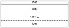
如图1所示,提供衬底1001。该衬底1001可以是各种形式的衬底,包括但不限于体半导体材料衬底如体Si衬底、绝缘体上半导体(SOI)衬底、化合物半导体衬底如SiGe衬底等。在以下的描述中,为方便说明,以体Si衬底为例进行描述。在此,提供硅晶片作为衬底1001。As shown in FIG. 1, a
在衬底1001中,例如可以通过离子注入,形成阱区1001-w。可以根据所要形成的器件类型,选择阱区1001-w的导电类型。例如,如果要形成的器件为p型器件(例如,pMOSFET),则可以形成n型阱区1001-w。n型阱区1001-w可以通过向衬底1001中注入n型杂质如磷(P)或砷(As)并通过退火来激活注入的杂质而形成。另一方面,如果要形成的器件为n型器件(例如,nMOSFET),则可以形成p型阱区1001-w。p型阱区1001-w可以通过向衬底1001中注入p型杂质如硼(B)并通过退火来激活注入的杂质而形成。In the
在衬底1001上,可以通过例如外延生长,依次形成牺牲层1003和预备半导体纳米结构层1005。On the
牺牲层1003可以具有所需的刻蚀选择性,例如相对于之下的衬底1001以及之上的预备半导体纳米结构层1005的刻蚀选择性,从而可以被选择性刻蚀。另外,考虑预备半导体纳米结构层1005的生长质量,牺牲层1003可以包括半导体材料。牺牲层1003可以具有与之下的衬底1001以及之上的预备半导体纳米结构层1005相同或基本相同的晶体结构。例如,牺牲层1003可以包括SiGe,Ge的原子百分比可以为约10-30%。牺牲层1003的厚度可以根据随后将要形成的环绕栅极的尺寸来确定,例如为约30-60nm。The
预备半导体纳米结构层1005可以包括半导体材料例如Si,随后可以形成器件的沟道。可以根据器件的沟道尺寸来确定预备半导体纳米结构层1005的尺寸,特别是其厚度(图中竖直方向上的维度)。例如,预备半导体纳米结构层1005的厚度为约5-15nm。The preparatory
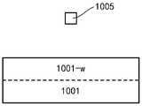
可以在预备半导体纳米结构层1005中限定所需的沟道形式,例如纳米线或纳米片。这可以通过对预备半导体纳米结构层1005构图来实现。例如,这可以如下进行。The desired channel form, such as nanowires or nanosheets, can be defined in the preparatory
如图2所示,可以在预备半导体纳米结构层1005上形成掩模层1007如光刻胶。可以通过光刻将光刻胶1007构图为限定所需的沟道形式。在该示例中,光刻胶1007的中部为线状,以便随后在预备半导体纳米结构层1005中限定纳米线。但是,本公开不限于此。例如,光刻胶可以限定矩形或方形,以便在预备半导体纳米结构层1005中限定纳米片。另外,光刻胶1007的两端覆盖预备半导体纳米结构层1005,以便限定支撑部,以支撑在后继工艺中将与衬底1001相分离的纳米线。As shown in FIG. 2 , a
然后,可以将光刻胶1007的图案转移到预备半导体纳米结构层1005中。如图3(a)、3(b)、3(c)和3(d)(图3(a)是俯视图,图3(b)是沿图3(a)中AA′线的截面图,图3(c)是沿图3(a)中B1B1′线的截面图,图3(d)是沿图3(a)中B2B2′线的截面图)所示,可以光刻胶1007作为刻蚀掩模,对预备半导体纳米结构层1005进行选择性刻蚀如反应离子刻蚀(RIE)。RIE可以沿竖直方向(例如,大致垂直于衬底表面的方向)进行。于是,预备半导体纳米结构层1005可以呈现与光刻胶1007基本上相同的图案。另外,可以对牺牲层1003进行选择性刻蚀如RIE。而且,在刻蚀过程中,可以使得在预备半导体纳米结构层1005下方,在牺牲层1003中出现底切,从而可以将预备半导体纳米结构层1005与衬底1001相分离。于是,形成了相对于衬底1001悬置的预备纳米线(预备半导体纳米结构层1005的中部),该预备纳米线在两端通过牺牲层1003支撑在衬底1001上。之后,可以去除光刻胶1007。Then, the pattern of
在以上通过牺牲层来形成悬置结构。由于牺牲层可以通过外延生长来形成,故而其尺寸控制较好。但是,本公开不限于此。本领域存在多种方式来形成悬置结构。例如,可以使衬底1001的表面部分变性从而相对于其下部具备刻蚀选择性,表面的变性部分可以类似于上述系数层1003起作用。The suspension structure is formed above through the sacrificial layer. Since the sacrificial layer can be formed by epitaxial growth, its size is better controlled. However, the present disclosure is not limited thereto. There are various ways in the art to form suspension structures. For example, the surface portion of the
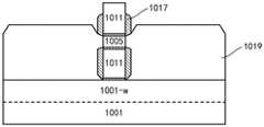
为形成具有自对准特征的栅堆叠,可以限定栅堆叠的位置。可以利用伪栅结构来占据栅堆叠的位置,在经过一系列处理之后,再将伪栅结构替换为栅堆叠。例如,这可以如下进行。To form a gate stack with self-aligned features, the location of the gate stack can be defined. The position of the gate stack can be occupied by the dummy gate structure, and after a series of processing, the dummy gate structure is replaced with the gate stack. For example, this can be done as follows.
如图4所示,可以在图3(a)、3(b)、3(c)和3(d)所示的结构上,例如通过淀积,形成环绕上述悬置预备纳米线的伪栅层1011。伪栅层1011可以包括提供所需刻蚀选择性的材料,例如氧化物(例如,氧化硅)。在该示例中,伪栅层1011填满了预备纳米线下方、牺牲层1003中的空间,并且还覆盖预备半导体纳米结构层1005的基本上全部顶面。可以对伪栅层1011进行平坦化处理如化学机械抛光(CMP)。As shown in FIG. 4, a dummy gate surrounding the above-mentioned suspended preparatory nanowires may be formed on the structures shown in FIGS. 3(a), 3(b), 3(c) and 3(d), for example, by
另外,为了保护预备纳米线,在形成伪栅层1011之前,可以先绕预备纳米线的外周形成保护层1009。保护层1009可以包括提供所需刻蚀选择性的材料,例如HfO2。保护层1009可以为一薄膜,例如大致共形地形成。In addition, in order to protect the preliminary nanowire, before forming the
在此,所谓“所需刻蚀选择性”,本领域技术人员可以根据上下文理解其含义。例如,当描述“对某一层进行选择性刻蚀”时,该层相对于暴露于对该层进行刻蚀的刻蚀配方中的其他层可以具有刻蚀选择性。Here, the so-called "required etching selectivity" can be understood by those skilled in the art according to the context. For example, when it is described that "a layer is selectively etched," the layer may have etch selectivity relative to other layers exposed to the etch recipe in which the layer is etched.
可以将伪栅层1011构图为伪栅结构。例如,伪栅结构可以与最终将用作沟道的纳米线相交(例如,各自的纵向延伸方向彼此大致垂直),以便在纳米线中限定沟道区。The
例如,如图5所示,可以在伪栅层1011上形成掩模层1013例如光刻胶。可以通过光刻将光刻胶1013构图为限定所需的栅形式,例如纵向沿与预备纳米线的纵向延伸方向(图5中的水平方向)相交(例如,大致垂直)的方向(图5中的竖直方向)延伸的棒状。For example, as shown in FIG. 5 , a
然后,可以将光刻胶1013的图案转移到伪栅层1011中以形成伪栅结构。如图6(a)和6(b)(图6(a)是俯视图,图6(b)是截面图,截取位置为前面示出的AA′线)所示,可以光刻胶1013为刻蚀掩模,对伪栅层1011进行选择性刻蚀如RIE。RIE可以沿竖直方向(例如,大致垂直于衬底表面的方向)进行。于是,伪栅层1011在俯视图中呈现与光刻胶1013基本上相同的棒状,且环绕预备纳米线。Then, the pattern of
另外,可以依次对保护层1009、预备半导体纳米结构层1005、牺牲层1003进行选择性刻蚀如RIE。RIE同样可以沿竖直方向(例如,大致垂直于衬底表面的方向)进行。于是,预备半导体纳米结构层1005留下的部分形成了纳米线(仍然标注为“1005”),该纳米线被伪栅层1011所围绕,且由伪栅层1011支撑在衬底1001上。另外,牺牲层1003已被完全去除。之后,可以去除光刻胶1013。In addition, the
由于采用同一掩模层1013作为刻蚀掩模进行刻蚀,因此,伪栅层1011中位于纳米线1005上方的部分和位于纳米线1005下方的部分可以自对准。即,上下两部分的至少部分侧壁可以在竖直方向上实质上对齐或者说共面。此外,伪栅层1011可以自对准于纳米线1005(随后将形成沟道)。因此,可以得到自对准环绕栅极(self-aligned wrapped aroundgate,SWAG)结构。由于这种SWAG结构是通过光刻得到的,其尺寸(特别是图中水平方向上的尺寸)可以得到很好地控制,且因此可以很好地控制器件的栅长,这对于大规模制造而言是有利的。Since the
通过以上处理,得到了自对准的沟道和(伪)栅结构。接下来,可以在沟道即纳米线1005两端形成源/漏区。例如,源/漏区可以通过在纳米线1005两端形成掺杂半导体材料来形成。为便于源/漏区的形成以及随后伪栅结构的替换,可以在伪栅层1011的侧壁上形成侧墙(spacer)。为了在伪栅层1011的侧壁上形成侧墙而并不在纳米线1005的侧壁上形成侧墙,可以在纳米线1005两端设置横向延伸部分。因为按照侧墙形成工艺,侧墙可以在竖直侧壁上形成,而并不形成在横向表面上。由于纳米线1005两端的横向延伸部分,侧墙可以不形成在纳米线1005的侧壁上。Through the above process, a self-aligned channel and (dummy) gate structure is obtained. Next, source/drain regions may be formed at both ends of the channel, ie, the
例如,如图7所示,可以通过选择性外延生长,从纳米线1005的侧壁生长外延层1015。生长可以纳米线1005(在此为Si)和衬底1001(在此也为Si)的露出表面为种子。外延层1015可以包括与纳米线1005相同的半导体材料,例如Si。当然,本公开不限于此。例如,外延层1015可以包括与纳米线1005不同的半导体材料,例如晶格常数不同的半导体材料以便向纳米线1005中施加应力。外延层1015可以生长一定的厚度,例如约10-30nm。在纳米线1005的两端生长的外延层1015由于其表面取向而可以呈现纺锤状。具体地,外延层1015为朝外侧先扩张然后渐缩的形状。For example, as shown in FIG. 7,
外延层1015随后可以用来形成延伸区(extension)。为此,可以对外延层1015进行一定导电类型的掺杂。例如,对于n型器件,可以利用n型杂质如P或As进行n型掺杂,而对于p型器件,可以利用p型杂质如B进行p型掺杂。可以在生长外延层1015的同时进行原位掺杂。
接下来,可以进行侧墙形成工艺。Next, a sidewall forming process may be performed.
例如,如图8所示,在图7所示的结构上,通过例如淀积,以大致共形的方式形成侧墙材料层1017。例如,侧墙材料层1017可以包括具有所需刻蚀选择性的材料如氮化物(例如,氮化硅),厚度为约5-20nm。可以对侧墙材料层1017进行选择性刻蚀如RIE。RIE可以沿着竖直方向(例如,大致垂直于衬底表面的方向)进行,以便去除侧墙材料层1017的横向延伸部分,而留下其竖直延伸部分。纳米线1005两端的外延层1015的上表面上的侧墙材料层1017可以被去除,其竖直侧壁上的侧墙材料层1017由于其高度较低从而甚至可能被完全去除,但是其下表面上的侧墙材料层1017可能留下。可以对外延层1015进行选择性刻蚀如RIE,RIE可以沿着竖直方向(例如,大致垂直于衬底表面的方向)进行。外延层1015靠近纳米线1015端面的部分由于被上方的侧墙材料层1017所遮挡从而可以保留,而外延层1015远离纳米线1015端面的部分由于外露而可以被去除,并因此露出了其下方的侧墙材料层1017。然后,进一步对侧墙材料层1017进行竖直方向的RIE。这样,就得到了如图9所示的侧墙,在此仍然标注为1017。可能仍有部分外延层1015留于衬底1001的表面。For example, as shown in FIG. 8, on the structure shown in FIG. 7, a layer of
按照上述工艺,侧墙1017自对准于伪栅结构,环绕纳米线1005端部的外延层1015。也即,形成了自对准环绕侧墙1017。另外,侧墙1017位于纳米线外延层1015上方的部分和位于外延层1015下方的部分也可以是彼此自对准的。外延层1015可以呈现朝向外侧扩张的形状,且被侧墙1017所环绕,这有助于降低寄生电阻。According to the above process, the
之后,可以在外延层1015(用作延伸区)的外侧进一步形成源/漏区。这里需要指出的是,延伸区也可以视为源/漏区的一部分。After that, source/drain regions may be further formed on the outside of the epitaxial layer 1015 (serving as extension regions). It should be pointed out here that the extension region can also be regarded as a part of the source/drain region.
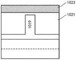
例如,如图10(a)和10(b)(图10(a)是俯视图,图10(b)是截面图,截取位置为前面示出的AA′线)所示,可以通过选择性外延生长,从外延层1015的侧壁生长外延层1019。生长可以纳米线1005两端的外延层1015(在此为Si)和衬底1001(在此也为Si)或衬底上1001上留下的外延层1015的露出表面为种子。外延层1019可以包括与纳米线1005相同的半导体材料,例如Si。当然,本公开不限于此。例如,外延层1019可以包括与纳米线1005不同的半导体材料,例如晶格常数不同的半导体材料以便向纳米线1005中施加应力。For example, as shown in Figs. 10(a) and 10(b) (Fig. 10(a) is a top view, Fig. 10(b) is a cross-sectional view, and the interception position is the line AA' shown earlier), selective epitaxy can be achieved by selective epitaxy. Growth,
可以对外延层1019进行掺杂以形成源/漏区。例如,对于n型器件,可以利用n型杂质如P或As进行n型掺杂,而对于p型器件,可以利用p型杂质如B进行p型掺杂。可以在生长外延层1019的同时进行原位掺杂。The
在此,进行较多的生长,获得较大的外延层1019,以便于后继的处理。在该示例中,从纳米线1005两端的外延层1015生长的外延层1019与从衬底1001表面生长的外延层1019可以彼此融合。另外,为便于后继处理,外延层1019的顶面可以低于侧墙1017的顶面。Here, more growth is performed to obtain a
至此,已经基本完成了器件的制作。在此,还可以应用应力源/漏技术。So far, the fabrication of the device has been basically completed. Here, stress source/drain techniques can also be applied.
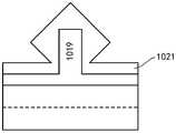
为更好地施加应力,可以将外延层1019构图为鳍状。例如,如图11所示,可以在图10(a)和10(b)所示的结构上形成掩模层1031例如光刻胶。可以通过光刻将光刻胶1031构图为鳍状。在该示例中,鳍状的光刻胶1031的纵向延伸方向可以与纳米线1005的纵向延伸方向(图中水平方向)基本上一致。另外,在俯视图中,光刻胶1031与纳米线1005、纳米线两端的外延层1015重叠。这样,随后通过光刻胶1031限定的源/漏区可以与纳米线1005两端的外延层1015相接。然后,如图12(a)、12(b)和12(c)(图12(a)是俯视图,图12(b)和12(c)是截面图,截取位置分别为前面示出的AA′线和B2B2′线)所示,可以光刻胶1031为刻蚀掩模,对外延层1019进行选择性刻蚀如反应离子刻蚀(RIE)。RIE可以沿竖直方向(例如,大致垂直于衬底表面的方向)进行。于是,外延层1019可以呈现与光刻胶1031基本相同的图案,在此为鳍状。另外,在对外延层1019进行刻蚀时,刻蚀可以没有进行到外延层1019的底面处,从而在衬底1001的表面上仍留有一定厚度的外延层1019,如图12(c)所示。之后,可以去除光刻胶1031。For better stress application, the
在外延层1019上可以形成应力层,以向纳米线1005施加应力。例如,如图13(a)、13(b)和13(c)(图13(a)是俯视图,图13(b)和13(c)是截面图,截取位置分别为前面示出的AA′线和B2B2′线)所示,可以通过外延生长,在外延层1019上形成应力层1021。例如,应力层1021可以包括晶格常数与外延层1019不同的半导体材料。对于p型器件,应力层1021可以施加压应力。例如,在外延层1019为Si的情况下,应力层1021可以包括SiGe,Ge的原子百分比可以为约10-70%。另一方面,而对于n型器件,应力层1021可以施加拉应力。例如,在外延层1019为Si的情况下,应力层1021可以包括Si:C,C的原子百分比为约0.3-2%。A stressor layer may be formed on the
图13(d)(沿B2B2′线的截面图)示出了生长的应力层1021的另一示例。FIG. 13(d) (a cross-sectional view along the line B2B2') shows another example of the
可以看到,由于外延层1019形成为鳍状,从而应力层可以绕其顶面和侧壁形成,从而可以更有效地施加应力。为便于后继处理,应力层1021的顶面可以低于侧墙1017的顶面。It can be seen that since the
接下来,可以将伪栅结构替换为栅堆叠。Next, the dummy gate structure can be replaced with a gate stack.
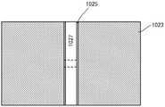
例如,如图14(a)和14(b)(图14(a)是俯视图,图14(b)是截面图,截取位置为前面示出的AA′线)所示,可以在图13(a)、13(b)和13(c)(或13(d))所示的结构上,例如通过淀积,形成电介质层1023。电介质层1023可以覆盖外延层1021,以在后继工艺中保护外延层1021。另外,电介质层1023可以占据侧墙1017外侧的空间,以避免栅堆叠形成在侧墙1017外侧。例如,电介质层1023可以包括氮化物(在此由于侧墙1017包括相同的材料,因此将侧墙1017与电介质层1023示出为一体)。淀积的电介质层1023可以超出侧墙1017的顶面,并可以对淀积的电介质层1023进行平坦化处理如CMP,CMP可以停止于侧墙1017,从而露出伪栅层1011。For example, as shown in Figures 14(a) and 14(b) (Figure 14(a) is a top view, Figure 14(b) is a cross-sectional view, and the interception position is the line AA' shown earlier), it can be shown in Figure 13 ( On the structures shown in a), 13(b) and 13(c) (or 13(d)), a
之后,可以去除伪栅层1011,并在由于伪栅层1011的去除而在侧墙内侧留下的空间中形成栅堆叠。如图15(a)和15(b)(图15(a)是俯视图,图15(b)是截面图,截取位置为前面示出的AA′线)所示,可以通过选择性刻蚀如RIE,去除伪栅层1011。在此,为了栅堆叠与衬底1001之间的电隔离,可以在底部(靠近衬底1001一侧)留下一定厚度的伪栅层1011(在此为氧化物)。对于纳米线1005下方的伪栅层1011,可以通过各向同性刻蚀予以去除。类似地,可以通过选择性刻蚀如RIE,去除保护层1009。这样,露出了纳米线1005。然后,如图16(a)、16(b)和16(c)(图16(a)是俯视图,图16(b)和16(c)是截面图,截取位置分别为前面示出的AA′线和B2B2′线)所示,可以在依次淀积栅介质层1025和栅导体层1027。例如,栅介质层1025可以包括高K栅介质如HfO2;栅导体层1027可以包括金属栅导体。优选地,栅介质层1025可以具有2-5nm的厚度。在形成栅介质层1025之前,还可以形成例如氧化物的界面层(未示出),氧化物界面层的厚度可以是0.3nm-1nm。另外,在栅介质层1025和栅导体层1027之间还可以存在功函数调节层(未示出)。栅介质层1025可以大致共形的方式形成,栅导体层1027可以填满侧墙内侧的空间。之后,可以对栅导体层1027和栅介质层1025进行平坦化处理例如CMP,CMP可以停止于电介质层1023,从而去除栅导体层1027和栅介质层1025位于侧墙之外的部分。After that, the
如图16(a)、16(b)和16(c)所示,根据本实施例的半导体器件可以包括半导体纳米结构1005(在该示例中,为纳米线)以及环绕半导体纳米结构1005的外周形成的栅堆叠。如上所述,由于伪栅层以自对准方式形成,因此占据伪栅层位置的栅堆叠也是自对准的,从而形成了SWAG。As shown in FIGS. 16( a ), 16 ( b ) and 16 ( c ), a semiconductor device according to the present embodiment may include a semiconductor nanostructure 1005 (in this example, a nanowire) and a periphery surrounding the
尽管在以上实施例中描述了单根纳米线的器件,但是本公开不限于此。例如,通过在衬底上交替堆叠牺牲层1003和半导体纳米结构层1005。在去除牺牲层1003之后,可以形成中部彼此分离的多个半导体纳米结构层1005并由此可以得到彼此间隔开的多个半导体纳米结构如纳米线或纳米片。可以按照同样的方式来形成伪栅层,伪栅层可以环绕这多个半导体纳米结构。随后,可以同样地将伪栅层替换为栅堆叠。Although a single nanowire device is described in the above embodiments, the present disclosure is not limited thereto. For example, by alternately stacking
根据本公开实施例的半导体器件可以应用于各种电子设备。例如,通过集成多个这样的半导体器件以及其他器件(例如,其他形式的晶体管等),可以形成集成电路(IC),并由此构建电子设备。因此,本公开还提供了一种包括上述半导体器件的电子设备。电子设备还可以包括与集成电路配合的显示屏幕以及与集成电路配合的无线收发器等部件。这种电子设备例如智能电话、计算机、平板电脑(PC)、人工智能、可穿戴设备、移动电源等。The semiconductor device according to the embodiment of the present disclosure can be applied to various electronic devices. For example, by integrating a plurality of such semiconductor devices, as well as other devices (eg, other forms of transistors, etc.), integrated circuits (ICs) may be formed and electronic devices constructed therefrom. Accordingly, the present disclosure also provides an electronic device including the above-described semiconductor device. The electronic device may also include components such as a display screen cooperating with the integrated circuit and a wireless transceiver cooperating with the integrated circuit. Such electronic devices are, for example, smartphones, computers, tablet computers (PCs), artificial intelligence, wearable devices, power banks, and the like.
在以上的描述中,对于各层的构图、刻蚀等技术细节并没有做出详细的说明。但是本领域技术人员应当理解,可以通过各种技术手段,来形成所需形状的层、区域等。另外,为了形成同一结构,本领域技术人员还可以设计出与以上描述的方法并不完全相同的方法。另外,尽管在以上分别描述了各实施例,但是这并不意味着各个实施例中的措施不能有利地结合使用。In the above description, technical details such as patterning and etching of each layer are not described in detail. However, those skilled in the art should understand that various technical means can be used to form layers, regions, etc. of desired shapes. In addition, in order to form the same structure, those skilled in the art can also design methods that are not exactly the same as those described above. Additionally, although the various embodiments have been described above separately, this does not mean that the measures in the various embodiments cannot be used in combination to advantage.
以上对本公开的实施例进行了描述。但是,这些实施例仅仅是为了说明的目的,而并非为了限制本公开的范围。本公开的范围由所附权利要求及其等价物限定。不脱离本公开的范围,本领域技术人员可以做出多种替代和修改,这些替代和修改都应落在本公开的范围之内。Embodiments of the present disclosure have been described above. However, these examples are for illustrative purposes only, and are not intended to limit the scope of the present disclosure. The scope of the present disclosure is defined by the appended claims and their equivalents. Without departing from the scope of the present disclosure, those skilled in the art can make various substitutions and modifications, and these substitutions and modifications should all fall within the scope of the present disclosure.
Claims (20)
Priority Applications (1)
| Application Number | Priority Date | Filing Date | Title |
|---|---|---|---|
| CN201811264731.1ACN109411539B (en) | 2018-10-26 | 2018-10-26 | Semiconductor device, method of manufacturing the same, and electronic apparatus including the same |
Applications Claiming Priority (1)
| Application Number | Priority Date | Filing Date | Title |
|---|---|---|---|
| CN201811264731.1ACN109411539B (en) | 2018-10-26 | 2018-10-26 | Semiconductor device, method of manufacturing the same, and electronic apparatus including the same |
Publications (2)
| Publication Number | Publication Date |
|---|---|
| CN109411539A CN109411539A (en) | 2019-03-01 |
| CN109411539Btrue CN109411539B (en) | 2022-04-19 |
Family
ID=65469495
Family Applications (1)
| Application Number | Title | Priority Date | Filing Date |
|---|---|---|---|
| CN201811264731.1AActiveCN109411539B (en) | 2018-10-26 | 2018-10-26 | Semiconductor device, method of manufacturing the same, and electronic apparatus including the same |
Country Status (1)
| Country | Link |
|---|---|
| CN (1) | CN109411539B (en) |
Families Citing this family (3)
| Publication number | Priority date | Publication date | Assignee | Title |
|---|---|---|---|---|
| CN111463287B (en)* | 2020-04-10 | 2024-02-27 | 中国科学院微电子研究所 | Semiconductor device, method of manufacturing the same, and electronic apparatus including the same |
| CN112018184B (en)* | 2020-09-07 | 2022-07-08 | 中国科学院微电子研究所 | Device with ferroelectric or negative capacitance material and its manufacturing method and electronic device |
| WO2022087782A1 (en)* | 2020-10-26 | 2022-05-05 | 中国科学院微电子研究所 | Pressure sensor based on zinc oxide nanowires and manufacturing method therefor |
Citations (4)
| Publication number | Priority date | Publication date | Assignee | Title |
|---|---|---|---|---|
| CN104701171A (en)* | 2013-12-05 | 2015-06-10 | 中芯国际集成电路制造(上海)有限公司 | Fin field-effect transistor and forming method thereof |
| CN104733311A (en)* | 2013-12-18 | 2015-06-24 | 中芯国际集成电路制造(上海)有限公司 | Fin-type field effect transistor forming method |
| CN105609421A (en)* | 2015-12-07 | 2016-05-25 | 中国科学院微电子研究所 | Semiconductor device with self-aligned gate structure and method of manufacturing the same |
| US9865681B1 (en)* | 2017-03-08 | 2018-01-09 | Globalfoundries Inc. | Nanowire transistors having multiple threshold voltages |
Family Cites Families (2)
| Publication number | Priority date | Publication date | Assignee | Title |
|---|---|---|---|---|
| US8685823B2 (en)* | 2011-11-09 | 2014-04-01 | International Business Machines Corporation | Nanowire field effect transistor device |
| US9929266B2 (en)* | 2016-01-25 | 2018-03-27 | International Business Machines Corporation | Method and structure for incorporating strain in nanosheet devices |
- 2018
- 2018-10-26CNCN201811264731.1Apatent/CN109411539B/enactiveActive
Patent Citations (4)
| Publication number | Priority date | Publication date | Assignee | Title |
|---|---|---|---|---|
| CN104701171A (en)* | 2013-12-05 | 2015-06-10 | 中芯国际集成电路制造(上海)有限公司 | Fin field-effect transistor and forming method thereof |
| CN104733311A (en)* | 2013-12-18 | 2015-06-24 | 中芯国际集成电路制造(上海)有限公司 | Fin-type field effect transistor forming method |
| CN105609421A (en)* | 2015-12-07 | 2016-05-25 | 中国科学院微电子研究所 | Semiconductor device with self-aligned gate structure and method of manufacturing the same |
| US9865681B1 (en)* | 2017-03-08 | 2018-01-09 | Globalfoundries Inc. | Nanowire transistors having multiple threshold voltages |
Also Published As
| Publication number | Publication date |
|---|---|
| CN109411539A (en) | 2019-03-01 |
Similar Documents
| Publication | Publication Date | Title |
|---|---|---|
| US11152516B2 (en) | Nanometer semiconductor devices having high-quality epitaxial layer | |
| US9230989B2 (en) | Hybrid CMOS nanowire mesh device and FINFET device | |
| TWI642181B (en) | Iii-v gate all around semiconductor device and method for manufaturing the same | |
| US11532753B2 (en) | Nanowire semiconductor device having high-quality epitaxial layer and method of manufacturing the same | |
| CN105633167B (en) | Semiconductor device with high-quality epitaxial layer and method of making the same | |
| CN108231864B (en) | Semiconductor device and method of manufacturing the same | |
| US20180315837A1 (en) | Finfet device with a reduced width | |
| CN109411539B (en) | Semiconductor device, method of manufacturing the same, and electronic apparatus including the same | |
| CN109888001B (en) | Semiconductor device, method for manufacturing the same, and electronic equipment including the same | |
| CN112018186A (en) | Nanowire/chip device with self-aligned isolation, manufacturing method and electronic equipment | |
| CN105977299B (en) | Semiconductor device and method for manufacturing the same | |
| CN111477684A (en) | Semiconductor device having U-shaped structure, method of manufacturing the same, and electronic apparatus | |
| CN112582464B (en) | Strained vertical channel semiconductor device, method of manufacturing the same, and electronic apparatus including the same | |
| CN106098776B (en) | Nanowire semiconductor device with high-quality epitaxial layer and method of making the same | |
| WO2017096780A1 (en) | Semiconductor device having high-quality epitaxial layer and method for manufacturing same | |
| CN111106165B (en) | U-shaped channel semiconductor device, manufacturing method thereof, and electronic equipment including the same | |
| CN111063728B (en) | C-shaped active region semiconductor device, method of manufacturing the same, and electronic apparatus including the same | |
| CN103681342B (en) | A kind of conducting channel preparation method | |
| CN111244161B (en) | C-shaped channel semiconductor device and electronic apparatus including the same | |
| CN105870062A (en) | High quality nanowire CMOS device, method of manufacturing the same, and electronic apparatus including the same | |
| CN111063684B (en) | Semiconductor device having C-shaped active region and electronic apparatus including the same | |
| CN105932057B (en) | Epitaxial layer-based nanowire device, method of making the same, and electronic device including the same | |
| CN114093949B (en) | GIDL-suppressing MOSFET, method of manufacturing the same, and electronic device including the same | |
| CN106024713A (en) | Semiconductor device, preparation method therefor, and electronic device | |
| CN116666439B (en) | Vertical semiconductor device having continuous gate length, method of manufacturing the same, and electronic apparatus |
Legal Events
| Date | Code | Title | Description |
|---|---|---|---|
| PB01 | Publication | ||
| PB01 | Publication | ||
| SE01 | Entry into force of request for substantive examination | ||
| SE01 | Entry into force of request for substantive examination | ||
| GR01 | Patent grant | ||
| GR01 | Patent grant |