CN109388173B - Current Compensation Circuit - Google Patents
Current Compensation CircuitDownload PDFInfo
- Publication number
- CN109388173B CN109388173BCN201710811829.3ACN201710811829ACN109388173BCN 109388173 BCN109388173 BCN 109388173BCN 201710811829 ACN201710811829 ACN 201710811829ACN 109388173 BCN109388173 BCN 109388173B
- Authority
- CN
- China
- Prior art keywords
- amplifier
- current
- circuit
- transistor
- voltage
- Prior art date
- Legal status (The legal status is an assumption and is not a legal conclusion. Google has not performed a legal analysis and makes no representation as to the accuracy of the status listed.)
- Active
Links
- 238000001514detection methodMethods0.000claimsabstractdescription140
- 238000006243chemical reactionMethods0.000claimsabstractdescription72
- 238000012937correctionMethods0.000claimsdescription19
- 239000003990capacitorSubstances0.000claimsdescription6
- 230000007423decreaseEffects0.000claimsdescription5
- 230000003044adaptive effectEffects0.000description45
- 238000010586diagramMethods0.000description16
- 101001064870Homo sapiens Lon protease homolog, mitochondrialProteins0.000description15
- 101000595531Homo sapiens Serine/threonine-protein kinase pim-1Proteins0.000description15
- 102100036077Serine/threonine-protein kinase pim-1Human genes0.000description15
- 241001125929Trisopterus luscusSpecies0.000description15
- 229920006395saturated elastomerPolymers0.000description8
- 101001001648Homo sapiens Serine/threonine-protein kinase pim-2Proteins0.000description6
- 102100036120Serine/threonine-protein kinase pim-2Human genes0.000description6
- 238000013461designMethods0.000description5
- 238000013459approachMethods0.000description3
- 230000003247decreasing effectEffects0.000description3
- 230000005540biological transmissionEffects0.000description1
- 230000000694effectsEffects0.000description1
- 238000000034methodMethods0.000description1
Images


Classifications
- H—ELECTRICITY
- H03—ELECTRONIC CIRCUITRY
- H03F—AMPLIFIERS
- H03F3/00—Amplifiers with only discharge tubes or only semiconductor devices as amplifying elements
- H03F3/189—High-frequency amplifiers, e.g. radio frequency amplifiers
- H03F3/19—High-frequency amplifiers, e.g. radio frequency amplifiers with semiconductor devices only
- H—ELECTRICITY
- H03—ELECTRONIC CIRCUITRY
- H03F—AMPLIFIERS
- H03F3/00—Amplifiers with only discharge tubes or only semiconductor devices as amplifying elements
- H03F3/20—Power amplifiers, e.g. Class B amplifiers, Class C amplifiers
- H03F3/21—Power amplifiers, e.g. Class B amplifiers, Class C amplifiers with semiconductor devices only
- H03F3/211—Power amplifiers, e.g. Class B amplifiers, Class C amplifiers with semiconductor devices only using a combination of several amplifiers
- G—PHYSICS
- G05—CONTROLLING; REGULATING
- G05F—SYSTEMS FOR REGULATING ELECTRIC OR MAGNETIC VARIABLES
- G05F1/00—Automatic systems in which deviations of an electric quantity from one or more predetermined values are detected at the output of the system and fed back to a device within the system to restore the detected quantity to its predetermined value or values, i.e. retroactive systems
- G05F1/10—Regulating voltage or current
- G05F1/46—Regulating voltage or current wherein the variable actually regulated by the final control device is DC
- G05F1/56—Regulating voltage or current wherein the variable actually regulated by the final control device is DC using semiconductor devices in series with the load as final control devices
- G05F1/575—Regulating voltage or current wherein the variable actually regulated by the final control device is DC using semiconductor devices in series with the load as final control devices characterised by the feedback circuit
- H—ELECTRICITY
- H03—ELECTRONIC CIRCUITRY
- H03F—AMPLIFIERS
- H03F1/00—Details of amplifiers with only discharge tubes, only semiconductor devices or only unspecified devices as amplifying elements
- H03F1/02—Modifications of amplifiers to raise the efficiency, e.g. gliding Class A stages, use of an auxiliary oscillation
- H03F1/0205—Modifications of amplifiers to raise the efficiency, e.g. gliding Class A stages, use of an auxiliary oscillation in transistor amplifiers
- H03F1/0211—Modifications of amplifiers to raise the efficiency, e.g. gliding Class A stages, use of an auxiliary oscillation in transistor amplifiers with control of the supply voltage or current
- H03F1/0216—Continuous control
- H03F1/0233—Continuous control by using a signal derived from the output signal, e.g. bootstrapping the voltage supply
- H—ELECTRICITY
- H03—ELECTRONIC CIRCUITRY
- H03F—AMPLIFIERS
- H03F1/00—Details of amplifiers with only discharge tubes, only semiconductor devices or only unspecified devices as amplifying elements
- H03F1/08—Modifications of amplifiers to reduce detrimental influences of internal impedances of amplifying elements
- H03F1/14—Modifications of amplifiers to reduce detrimental influences of internal impedances of amplifying elements by use of neutralising means
- H—ELECTRICITY
- H03—ELECTRONIC CIRCUITRY
- H03F—AMPLIFIERS
- H03F3/00—Amplifiers with only discharge tubes or only semiconductor devices as amplifying elements
- H03F3/189—High-frequency amplifiers, e.g. radio frequency amplifiers
- H—ELECTRICITY
- H03—ELECTRONIC CIRCUITRY
- H03F—AMPLIFIERS
- H03F3/00—Amplifiers with only discharge tubes or only semiconductor devices as amplifying elements
- H03F3/189—High-frequency amplifiers, e.g. radio frequency amplifiers
- H03F3/19—High-frequency amplifiers, e.g. radio frequency amplifiers with semiconductor devices only
- H03F3/191—Tuned amplifiers
- H—ELECTRICITY
- H03—ELECTRONIC CIRCUITRY
- H03F—AMPLIFIERS
- H03F3/00—Amplifiers with only discharge tubes or only semiconductor devices as amplifying elements
- H03F3/20—Power amplifiers, e.g. Class B amplifiers, Class C amplifiers
- H03F3/21—Power amplifiers, e.g. Class B amplifiers, Class C amplifiers with semiconductor devices only
- H—ELECTRICITY
- H03—ELECTRONIC CIRCUITRY
- H03F—AMPLIFIERS
- H03F3/00—Amplifiers with only discharge tubes or only semiconductor devices as amplifying elements
- H03F3/20—Power amplifiers, e.g. Class B amplifiers, Class C amplifiers
- H03F3/24—Power amplifiers, e.g. Class B amplifiers, Class C amplifiers of transmitter output stages
- H03F3/245—Power amplifiers, e.g. Class B amplifiers, Class C amplifiers of transmitter output stages with semiconductor devices only
- H—ELECTRICITY
- H03—ELECTRONIC CIRCUITRY
- H03F—AMPLIFIERS
- H03F2200/00—Indexing scheme relating to amplifiers
- H03F2200/408—Indexing scheme relating to amplifiers the output amplifying stage of an amplifier comprising three power stages
- H—ELECTRICITY
- H03—ELECTRONIC CIRCUITRY
- H03F—AMPLIFIERS
- H03F2200/00—Indexing scheme relating to amplifiers
- H03F2200/451—Indexing scheme relating to amplifiers the amplifier being a radio frequency amplifier
- H—ELECTRICITY
- H03—ELECTRONIC CIRCUITRY
- H03F—AMPLIFIERS
- H03F2200/00—Indexing scheme relating to amplifiers
- H03F2200/456—A scaled replica of a transistor being present in an amplifier
Landscapes
- Engineering & Computer Science (AREA)
- Power Engineering (AREA)
- Physics & Mathematics (AREA)
- Electromagnetism (AREA)
- General Physics & Mathematics (AREA)
- Radar, Positioning & Navigation (AREA)
- Automation & Control Theory (AREA)
- Amplifiers (AREA)
- Microelectronics & Electronic Packaging (AREA)
- Nonlinear Science (AREA)
Abstract
Description
Translated fromChinese技术领域technical field
本发明涉及一种电流补偿电路,尤其涉及一种用以提供补偿电流来增加放大器电路的偏压电流的电流补偿电路。The invention relates to a current compensation circuit, in particular to a current compensation circuit for providing compensation current to increase the bias current of an amplifier circuit.
背景技术Background technique
功率放大器(Power Amplifier)是射频发射电路中一个重要的组件,其主要的功能在于将信号放大推出,通常都会被设计在天线放射器的前端,也是整个射频前端电路中最耗功耗的组件。功率放大器主要应用于需要带宽的电子产品或设备上,例如手机、平板计算机、卫星通讯等网通产品,其中手机为其最大的应用市场。Power amplifier (Power Amplifier) is an important component in the RF transmission circuit. Its main function is to amplify the signal and push it out. It is usually designed at the front end of the antenna radiator, and it is also the most power-consuming component in the entire RF front-end circuit. Power amplifiers are mainly used in electronic products or devices that require bandwidth, such as mobile phones, tablet computers, satellite communications and other Netcom products, of which mobile phones are the largest application market.
然而,功率放大器电路具有增益会随着其输出功率的增加而逐渐饱和且下降的特性,因此在输出功率较大时,功率放大器电路的线性度会较差,此种情况于多级放大器电路中尤其明显。However, the power amplifier circuit has the characteristic that the gain will gradually saturate and decrease with the increase of its output power, so when the output power is large, the linearity of the power amplifier circuit will be poor. Especially obvious.
发明内容SUMMARY OF THE INVENTION
本发明提供一种电流补偿电路,用以提供电流至一放大器电路。放大器电路包括第一放大器、第一晶体管与第一偏压电路。第一偏压电路提供第一偏压电流至第一放大器,且第一放大器透过第一晶体管耦接于一供应电压。此种电流补偿电路包括功率侦测电路、运算放大器电路与电压电流转换单元。功率侦测电路耦接于第一放大器,运算放大器电路耦接于功率侦测电路,且电压电流转换单元耦接于运算放大器电路与第一晶体管。功率侦测电路用以侦测第一放大器的输入功率或输出功率,并将所测得的功率值转换为一第一侦测电压。根据第一侦测电压与一校正电压,运算放大器电路输出第二侦测电压。电压电流转换单元用以将第二侦测电压转换为一补偿电流。根据此补偿电流,第一补偿电流对应地被产生并经由第一晶体管流向第一放大器。于是,第一放大器转为由第一偏压电流与第一补偿电流的和来驱动。The present invention provides a current compensation circuit for supplying current to an amplifier circuit. The amplifier circuit includes a first amplifier, a first transistor and a first bias circuit. The first bias circuit provides a first bias current to the first amplifier, and the first amplifier is coupled to a supply voltage through the first transistor. The current compensation circuit includes a power detection circuit, an operational amplifier circuit and a voltage-current conversion unit. The power detection circuit is coupled to the first amplifier, the operational amplifier circuit is coupled to the power detection circuit, and the voltage-current conversion unit is coupled to the operational amplifier circuit and the first transistor. The power detection circuit is used to detect the input power or output power of the first amplifier, and convert the measured power value into a first detection voltage. According to the first detection voltage and a correction voltage, the operational amplifier circuit outputs the second detection voltage. The voltage-current converting unit is used for converting the second detection voltage into a compensation current. According to this compensation current, a first compensation current is correspondingly generated and flows to the first amplifier via the first transistor. Thus, the first amplifier turns to be driven by the sum of the first bias current and the first compensation current.
本发明提供另一种电流补偿电路,用以提供电流至一放大器电路。放大器电路包括第一放大器、第一晶体管与第一偏压电路、第二放大器、第二晶体管与第二偏压电路以及第三放大器。第一偏压电路提供一第一偏压电流至第一放大器,且第二偏压电路提供一第二偏压电流至第二放大器。另外,第一放大器与第二放大器分别透过第一晶体管与第二晶体管耦接于一供应电压。此种电流补偿电路包括功率侦测电路、运算放大器电路与电压电流转换单元。功率侦测电路耦接于第一放大器的输出端或第二放大器的输出端,运算放大器电路连接于功率侦测电路,且电压电流转换单元耦接于运算放大器电路。此外,第一晶体管与第二晶体管分别连接于电压电流转换单元。功率侦测电路用以侦测第一放大器的输出功率或侦测第二放大器的输出功率,并将所测得的功率值转换为一第一侦测电压。根据第一侦测电压与一校正电压,运算放大器电路输出一第二侦测电压。电压电流转换单元将第二侦测电压转换为一补偿电流。根据该补偿电流,第一补偿电流被对应地产生并经由第一晶体管流向第一放大器,或者根据该补偿电流,第二补偿电流对应地被产生并经由第二晶体管流向第二放大器。于是,第一放大器转为由该第一偏压电流与第一补偿电流的和来驱动,或者第二放大器转为由该第二偏压电流与第二补偿电流的和来驱动。The present invention provides another current compensation circuit for supplying current to an amplifier circuit. The amplifier circuit includes a first amplifier, a first transistor and a first bias circuit, a second amplifier, a second transistor and a second bias circuit, and a third amplifier. The first bias circuit provides a first bias current to the first amplifier, and the second bias circuit provides a second bias current to the second amplifier. In addition, the first amplifier and the second amplifier are respectively coupled to a supply voltage through the first transistor and the second transistor. The current compensation circuit includes a power detection circuit, an operational amplifier circuit and a voltage-current conversion unit. The power detection circuit is coupled to the output end of the first amplifier or the output end of the second amplifier, the operational amplifier circuit is connected to the power detection circuit, and the voltage-current conversion unit is coupled to the operational amplifier circuit. In addition, the first transistor and the second transistor are respectively connected to the voltage-current converting unit. The power detection circuit is used to detect the output power of the first amplifier or the output power of the second amplifier, and convert the measured power value into a first detection voltage. According to the first detection voltage and a correction voltage, the operational amplifier circuit outputs a second detection voltage. The voltage-current converting unit converts the second detection voltage into a compensation current. Depending on the compensation current, a first compensation current is correspondingly generated and flows to the first amplifier via the first transistor, or a second compensation current is correspondingly generated and flows to the second amplifier via the second transistor. Then, the first amplifier turns to be driven by the sum of the first bias current and the first compensation current, or the second amplifier turns to be driven by the sum of the second bias current and the second compensation current.
本发明提供另一种电流补偿电路,用以提供电流至一放大器电路。放大器电路包括第一放大器、第一晶体管与第一偏压电路、第二放大器、第二晶体管与第二偏压电路以及第三放大器。第一偏压电路提供一第一偏压电流至第一放大器,且第二偏压电路提供一第二偏压电流至第二放大器。另外,第一放大器与第二放大器分别透过第一晶体管与第二晶体管耦接于一供应电压。此种电流补偿电路包括功率侦测电路、运算放大器电路与电压电流转换单元。功率侦测电路耦接于第一放大器的输出端或第二放大器的输出端,运算放大器电路连接于功率侦测电路,且电压电流转换单元耦接于运算放大器电路。此外,第一晶体管与第二晶体管分别连接于电压电流转换单元。功率侦测电路用以侦测第一放大器的输出功率或侦测第二放大器的输出功率,并将所测得的功率值转换为一第一侦测电压。根据第一侦测电压与一校正电压,运算放大器电路输出一第二侦测电压。电压电流转换单元将第二侦测电压转换为一补偿电流。根据该补偿电流,第一补偿电流被对应地产生并经由第一晶体管流向第一放大器,且根据该补偿电流,第二补偿电流对应地被产生并经由第二晶体管流向第二放大器。于是,第一放大器转为由该第一偏压电流与第一补偿电流的和来驱动,且第二放大器转为由该第二偏压电流与第二补偿电流的和来驱动。The present invention provides another current compensation circuit for supplying current to an amplifier circuit. The amplifier circuit includes a first amplifier, a first transistor and a first bias circuit, a second amplifier, a second transistor and a second bias circuit, and a third amplifier. The first bias circuit provides a first bias current to the first amplifier, and the second bias circuit provides a second bias current to the second amplifier. In addition, the first amplifier and the second amplifier are respectively coupled to a supply voltage through the first transistor and the second transistor. The current compensation circuit includes a power detection circuit, an operational amplifier circuit and a voltage-current conversion unit. The power detection circuit is coupled to the output end of the first amplifier or the output end of the second amplifier, the operational amplifier circuit is connected to the power detection circuit, and the voltage-current conversion unit is coupled to the operational amplifier circuit. In addition, the first transistor and the second transistor are respectively connected to the voltage-current converting unit. The power detection circuit is used to detect the output power of the first amplifier or the output power of the second amplifier, and convert the measured power value into a first detection voltage. According to the first detection voltage and a correction voltage, the operational amplifier circuit outputs a second detection voltage. The voltage-current converting unit converts the second detection voltage into a compensation current. According to the compensation current, a first compensation current is correspondingly generated and flows to the first amplifier via the first transistor, and according to the compensation current, a second compensation current is correspondingly generated and flows to the second amplifier via the second transistor. Thus, the first amplifier turns to be driven by the sum of the first bias current and the first compensation current, and the second amplifier turns to be driven by the sum of the second bias current and the second compensation current.
本发明提供另一种电流补偿电路,用以提供电流至一放大器电路。该放大器电路包括第一放大器与第一晶体管,且第一放大器透过第一晶体管耦接于一供应电压。此种电流补偿电路包括侦测电路、运算放大器电路与电压电流转换单元。侦测电路耦接于第一放大器,且运算放大器电路耦接于侦测电路。侦测电路用以根据第一放大器的输入信号的强度或输出信号的强度输出一第一侦测电压。根据第一侦测电压与一校正电压,运算放大器电路输出一第二侦测电压。电压电流转换单元用以将第二侦测电压转换为一补偿电流。电压电流转换单元包括转换晶体管,此转换晶体管具有第一端、第二端与第三端。转换晶体管的第一端耦接于供应电压,转换晶体管的第三端耦接于一参考电位,且转换晶体管的第二端耦接于运算放大器电路以及第一晶体管。另外,转换晶体管与第一晶体管形成一电流镜架构。The present invention provides another current compensation circuit for supplying current to an amplifier circuit. The amplifier circuit includes a first amplifier and a first transistor, and the first amplifier is coupled to a supply voltage through the first transistor. The current compensation circuit includes a detection circuit, an operational amplifier circuit and a voltage-current conversion unit. The detection circuit is coupled to the first amplifier, and the operational amplifier circuit is coupled to the detection circuit. The detection circuit is used for outputting a first detection voltage according to the strength of the input signal or the strength of the output signal of the first amplifier. According to the first detection voltage and a correction voltage, the operational amplifier circuit outputs a second detection voltage. The voltage-current converting unit is used for converting the second detection voltage into a compensation current. The voltage-current conversion unit includes a conversion transistor, and the conversion transistor has a first end, a second end and a third end. The first end of the conversion transistor is coupled to the supply voltage, the third end of the conversion transistor is coupled to a reference potential, and the second end of the conversion transistor is coupled to the operational amplifier circuit and the first transistor. In addition, the switching transistor and the first transistor form a current mirror structure.
本发明所提供的电流补偿电路能藉由侦测放大器电路的功率来提供适当的补偿电流给放大器电路中的各级放大器,使得放大器电路中各级放大器的偏压电流因补偿电流的加入而增大,以个别调整各级放大器的增益曲线。如此一来,即使放大器电路的输出功率逐渐增加,放大器电路整体的增益也不会出现渐趋饱和与下降的情形,使得放大器电路能具有良好的线性度。The current compensation circuit provided by the present invention can provide an appropriate compensation current to the amplifiers at all levels in the amplifier circuit by detecting the power of the amplifier circuit, so that the bias current of the amplifiers at each level in the amplifier circuit increases due to the addition of the compensation current. Large, to individually adjust the gain curve of each amplifier. In this way, even if the output power of the amplifier circuit is gradually increased, the overall gain of the amplifier circuit will not be gradually saturated and decreased, so that the amplifier circuit can have good linearity.
为使能更进一步了解本发明的特征及技术内容,请参阅以下有关本发明的详细说明与附图,但是此等说明与所附说明书附图仅是用来说明本发明,而非对本发明的权利要求书作任何的限制。In order to further understand the features and technical content of the present invention, please refer to the following detailed descriptions and accompanying drawings of the present invention, but these descriptions and accompanying drawings are only used to illustrate the present invention, not to the present invention. The claims do not impose any limitations.
附图说明Description of drawings
关于本发明的优点与精神可以通过以下的发明详述及所附图式得到进一步的了解。The advantages and spirit of the present invention can be further understood from the following detailed description of the invention and the accompanying drawings.
图1A为根据本发明示例性实施例绘示的电流补偿电路的应用示意方块图;1A is a schematic block diagram of an application of a current compensation circuit according to an exemplary embodiment of the present invention;
图1B为根据本发明另一示例性实施例绘示的电流补偿电路的应用示意方块图;1B is a schematic block diagram illustrating an application of a current compensation circuit according to another exemplary embodiment of the present invention;
图2为根据本发明另一示例性实施例绘示的电流补偿电路的应用示意方块图;2 is a schematic block diagram illustrating an application of a current compensation circuit according to another exemplary embodiment of the present invention;
图3为根据本发明另一示例性实施例绘示的电流补偿电路的应用示意方块图;3 is a schematic block diagram of an application of a current compensation circuit according to another exemplary embodiment of the present invention;
图4为图3所绘示的电流补偿电路的应用示意电路图;4 is a schematic circuit diagram of an application of the current compensation circuit shown in FIG. 3;
图5A~图5C为放大器电路的输出功率与各放大器的增益的关系图;5A to 5C are graphs showing the relationship between the output power of the amplifier circuit and the gain of each amplifier;
图6为根据本发明示例性实施例绘示的电流补偿电路中功率侦测电路的电路图;6 is a circuit diagram of a power detection circuit in a current compensation circuit according to an exemplary embodiment of the present invention;
图7A为根据本发明示例性实施例绘示的电流补偿电路中运算放大器电路的电路图;7A is a circuit diagram of an operational amplifier circuit in a current compensation circuit according to an exemplary embodiment of the present invention;
图7B为根据本发明另一示例性实施例绘示的电流补偿电路中运算放大器电路的电路图。7B is a circuit diagram of an operational amplifier circuit in a current compensation circuit according to another exemplary embodiment of the present invention.
主要图示说明:Main icon description:
10a:第一偏压电路10a: first bias circuit
10b:第二偏压电路10b: Second bias circuit
20:功率侦测电路20: Power detection circuit
20’:侦测电路20': detection circuit
30:运算放大器电路30: Operational amplifier circuit
40:电压电流转换单元40: Voltage and current conversion unit
PA1:第一放大器PA1: first amplifier
PA2:第二放大器PA2: Second amplifier
PA3:第三放大器PA3: The third amplifier
VDD:供应电源VDD: power supply
M1:第一晶体管M1: first transistor
M2:第二晶体管M2: second transistor
M3:转换晶体管M3: Conversion transistor
M4:第四晶体管M4: Fourth transistor
M5:第五晶体管M5: Fifth transistor
Ibias1:第一偏压电流Ibias1 : the first bias current
Ibias2:第二偏压电流Ibias2 : second bias current
Iadaptive:补偿电流Iadaptive : compensation current
N×Iadaptive:第一补偿电流N×Iadaptive : the first compensation current
M×Iadaptive:第二补偿电流M×Iadaptive : the second compensation current
PIN:输入功率PIN: input power
PIM1、PIM2、POUT:输出功率PIM1, PIM2, POUT: output power
GND:参考电位GND: reference potential
VPD:第一侦测电压VPD : the first detection voltage
Vdet:第二侦测电压Vdet : the second detection voltage
VPD_DC:校正电压VPD_DC : Correction voltage
C:电容器C: Capacitor
Rchoke:扼流电阻Rchoke : choke resistance
R1:第一电阻R1: first resistor
R2:第二电阻R2: second resistor
R3:第三电阻R3: third resistor
R4:第四电阻R4: Fourth resistor
g1、g2、g3、g4、g5、g6:曲线g1, g2, g3, g4, g5, g6: Curves
OP:运算放大器OP: Operational Amplifier
VA:第一参考电压VA: first reference voltage
VB:第二参考电压VB: The second reference voltage
具体实施方式Detailed ways
在下文将参看说明书附图更充分地描述各种示例性实施例,在说明书附图中展示一些示例性实施例。然而,本发明概念可能以许多不同形式来体现,且不应解释为限于本文中所阐述的示例性实施例。确切而言,提供此等示例性实施例使得本发明更为详尽且完整,且将向本领域技术人员充分传达本发明概念的范畴。在各说明书附图中,表示同一组成部分的附图标记始终一致。Various exemplary embodiments will be described more fully hereinafter with reference to the accompanying drawings in the specification, in which some exemplary embodiments are shown. The inventive concepts may, however, be embodied in many different forms and should not be construed as limited to the exemplary embodiments set forth herein. Rather, these exemplary embodiments are provided so that this disclosure will be thorough and complete, and will fully convey the scope of the inventive concept to those skilled in the art. In each of the drawings in the specification, the reference numerals denoting the same components are always the same.
本发明所提供的电流补偿电路主要用以提供补偿电流予一放大器电路,使得放大器的偏压电流因补偿电流的加入而增大,进而改善放大器电路的线性度。以下将以多个实施例说明本发明所提供的电流补偿电路,然而,下述实施例并非用以限制本发明。The current compensation circuit provided by the present invention is mainly used to provide a compensation current to an amplifier circuit, so that the bias current of the amplifier is increased due to the addition of the compensation current, thereby improving the linearity of the amplifier circuit. Hereinafter, the current compensation circuit provided by the present invention will be described with several embodiments, however, the following embodiments are not intended to limit the present invention.
〔电流补偿电路的一实施例〕[An example of a current compensation circuit]
请参照图1A,图1A为根据本发明示例性实施例绘示的电流补偿电路的应用示意方块图。Please refer to FIG. 1A . FIG. 1A is a schematic block diagram illustrating an application of a current compensation circuit according to an exemplary embodiment of the present invention.
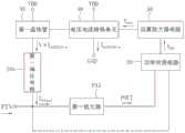
本实施例所提供的电流补偿电路能提供补偿电流给放大器电路。举例来说,放大器电路可以是如图1A所示的简单的放大器电路,此放大器电路包括第一放大器PA1、第一晶体管M1与第一偏压电路10a。第一放大器PA1包括输入端与输出端。于此放大器电路中,第一偏压电路10a提供第一偏压电流Ibias1至第一放大器PA1的输入端,且第一放大器PA1的输入端透过第一晶体管M1耦接于一供应电压VDD。The current compensation circuit provided in this embodiment can provide compensation current to the amplifier circuit. For example, the amplifier circuit can be a simple amplifier circuit as shown in FIG. 1A , and the amplifier circuit includes a first amplifier PA1 , a first transistor M1 and a
复如图1A所示,本实施例所提供的电流补偿电路包括功率侦测电路20、运算放大器电路30与电压电流转换单元40。功率侦测电路20耦接于第一放大器PA1的输入端或输出端,运算放大器电路30耦接于功率侦测电路20,且电压电流转换单元40耦接于运算放大器电路30。此外,电压电流转换单元40还耦接于放大器电路中的第一晶体管M1。As shown in FIG. 1A , the current compensation circuit provided in this embodiment includes a
由于第一放大器PA1的增益会随着其输出功率POUT或输入功率PIN的增加而逐渐饱和,因此在输出功率POUT或输入功率PIN较大时,第一放大器PA1的线性度会较差。本实施例所提供的电流补偿电路能够提供补偿电流予第一放大器PA1,使得第一放大器PA1的偏压电流因补偿电流的加入而增大,如此一来便能将第一放大器PA1原本逐渐饱和的增益拉高,进而改善第一放大器PA1的线性度(即,改善第一放大器PA1的输出功率与增益之间的关系)。Since the gain of the first amplifier PA1 will gradually saturate as its output power POUT or input power PIN increases, when the output power POUT or input power PIN is large, the linearity of the first amplifier PA1 will be poor. The current compensation circuit provided in this embodiment can provide a compensation current to the first amplifier PA1, so that the bias current of the first amplifier PA1 is increased due to the addition of the compensation current, so that the original first amplifier PA1 can be gradually saturated The gain of the first amplifier PA1 is increased, thereby improving the linearity of the first amplifier PA1 (ie, improving the relationship between the output power and the gain of the first amplifier PA1).
根据此原理,本实施例所提供的电流补偿电路所提供给第一放大器PA1的补偿电流应相关于第一放大器PA1的输出功率POUT或输入功率PIN。因此,为了能够提供足够的补偿电流给第一放大器PA1,于本实施例中,功率侦测电路20会侦测第一放大器PA1的输入端的输入功率PIN或输出端的输出功率POUT,并将所测得的功率值转换为第一侦测电压VPD。为了精确地得知要提供多少补偿电流给第一放大器PA1,运算放大器电路30会根据第一侦测电压VPD与一校正电压(图中未示出)产生第二侦测电压Vdet。According to this principle, the compensation current provided to the first amplifier PA1 by the current compensation circuit provided in this embodiment should be related to the output power POUT or the input power PIN of the first amplifier PA1. Therefore, in order to provide sufficient compensation current to the first amplifier PA1, in this embodiment, the
接着,电压电流转换单元40便将第二侦测电压Vdet转换为一补偿电流Iadaptive。举例来说,电压电流转换单元40可透过一电阻来将第二侦测电压Vdet转换为补偿电流Iadaptive。Then, the voltage-
当电压电流转换单元40将第二侦测电压转Vdet换为补偿电流Iadaptive时,根据补偿电流Iadaptive,第一补偿电流N×Iadaptive会对应地于放大器电路中产生并经由第一晶体管M1流向第一放大器PA1。于是,第一放大器PA1转为由第一偏压电流Ibias1与第一补偿电流N×Iadaptive的和来驱动。简言之,本实施例所提供的电流补偿电路提供第一补偿电流N×Iadaptive给第一放大器PA1,如此一来,用以驱动第一放大器PA1的偏压电流增加,使得第一放大器PA1原本逐渐饱和的增益被拉高,本实施例所提供的电流补偿电路也就能达到补偿放大器电路于输出功率饱和后下降的增益的功效。When the voltage-to-
需说明地是,于本实施例中,电压电流转换单元40可包括一晶体管,于是此晶体管与放大器电路中的第一晶体管M1便形成一电流镜架构,使得第一补偿电流N×Iadaptive正比于补偿电流Iadaptive(即,电流补偿电路应提供给第一放大器PA1的第一补偿电流N×Iadaptive为补偿电流Iadaptive的N倍)。值得注意地是,倍数N的大小决定了第一放大器PA1其增益被拉高的快慢。于本实施例中,较佳的作法是将拉高第一放大器PA1的增益的速率设计为原先第一放大器PA1的增益逐渐饱和的速率。此外,如前述,电压电流转换单元40与放大器电路中的第一晶体管M1形成一电流镜架构,因此倍数N的大小可透过电压电流转换单元40与第一晶体管M1两者的组件设计来调整。It should be noted that, in this embodiment, the voltage-to-
〔电流补偿电路的另一实施例〕[Another Example of Current Compensation Circuit]
请参照图1B,图1B为根据本发明另一示例性实施例绘示的电流补偿电路的应用示意方块图。Please refer to FIG. 1B , which is a schematic block diagram illustrating an application of a current compensation circuit according to another exemplary embodiment of the present invention.
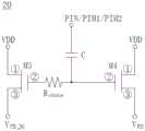
本实施例所提供的电流补偿电路能提供补偿电流给放大器电路。举例来说,放大器电路可以是如图1B所示的简单的放大器电路,此放大器电路包括第一放大器PA1与第一晶体管M1,第一放大器PA1包括输入端与输出端,且第一放大器PA1的输入端透过第一晶体管M1耦接于一供应电压VDD。The current compensation circuit provided in this embodiment can provide compensation current to the amplifier circuit. For example, the amplifier circuit may be a simple amplifier circuit as shown in FIG. 1B , the amplifier circuit includes a first amplifier PA1 and a first transistor M1 , the first amplifier PA1 includes an input terminal and an output terminal, and the first amplifier PA1 has an input terminal and an output terminal. The input terminal is coupled to a supply voltage VDD through the first transistor M1.
复如图1B所示,本实施例所提供的电流补偿电路包括侦测电路20’、运算放大器电路30与电压电流转换单元40。侦测电路20’耦接于第一放大器PA1的输入端或输出端,运算放大器电路30耦接于侦测电路20’,且电压电流转换单元40耦接于运算放大器电路30。As shown in FIG. 1B , the current compensation circuit provided in this embodiment includes a
于本实施例中,侦测电路20’会根据第一放大器PA1的输入端的输入信号的强度或输出端的输出信号的强度输出第一侦测电压VPD,接着,运算放大器电路30会根据第一侦测电压VPD与一校正电压(图中未示出)产生第二侦测电压Vdet,最后,电压电流转换单元40会将第二侦测电压Vdet转换为一电流(即如图1B所示的补偿电流Iadaptive)。In this embodiment, the
复如图1B所示,电压电流转换单元40包括一转换晶体管M3。转换晶体管M3具有第一端、第二端与第三端,转换晶体管M3的第一端耦接于供应电压VDD,转换晶体管M3的第三端耦接于一参考电位GND,转换晶体管M3的第二端耦接于运算放大器电路30以及放大器电路中的第一晶体管M1。为便于说明,于图1B中,转换晶体管M3的第一端标示为①,转换晶体管M3的第二端标示为②,转换晶体管M3的第三端标示为③。As shown in FIG. 1B , the voltage-to-
进一步说明,当转换晶体管M3的第二端接收到第二侦测电压Vdet时,根据欧姆定律,第二侦测电压Vdet会透过第一电阻R1转换为补偿电流Iadaptive。再者,由于转换晶体管M3与放大器电路中的第一晶体管M1形成了一个电流镜架构。因此,当电压电流转换单元40将第二侦测电压Vdet转换为补偿电流Iadaptive时,会有一电流于放大器电路侧产生,且此电流与补偿电流Iadaptive成正比,也就是说,此电流会是补偿电流Iadaptive的N倍。To further illustrate, when the second terminal of the conversion transistor M3 receives the second detection voltage Vdet , according to Ohm's law, the second detection voltage Vdet will be converted into the compensation current Iadaptive through the first resistor R1 . Furthermore, since the conversion transistor M3 and the first transistor M1 in the amplifier circuit form a current mirror structure. Therefore, when the voltage-to-
与图1A所绘示的电流补偿电路的差异在于,于本实施例中,透过转换晶体管M3与放大器电路中的第一晶体管M1所组成的电流镜架构所产生的电流(即,N倍的补偿电流Iadaptive)能够直接作为驱动第一放大器PA1的偏压电流,其中倍数N的大小可透过电压电流转换单元40与第一晶体管M1两者的组件设计来调整。The difference from the current compensation circuit shown in FIG. 1A is that, in this embodiment, the current generated by the current mirror structure composed of the conversion transistor M3 and the first transistor M1 in the amplifier circuit (ie, N times the The compensation current Iadaptive ) can be directly used as the bias current for driving the first amplifier PA1 , wherein the size of the multiple N can be adjusted through the component design of both the voltage-
因此,于本实施例中,若电流补偿电路所适用的放大器电路本身已包括有一偏压电路,第一放大器PA1则是由此偏压电路所提供的偏压电流以及透过转换晶体管M3与放大器电路中的第一晶体管M1所组成的电流镜架构所产生的电流共同来驱动第一放大器PA1。Therefore, in this embodiment, if the amplifier circuit to which the current compensation circuit is applied already includes a bias circuit, the first amplifier PA1 is the bias current provided by the bias circuit and passes through the conversion transistor M3 and the amplifier The currents generated by the current mirror structure formed by the first transistor M1 in the circuit together drive the first amplifier PA1.
除此之外,于本实施例中,侦测电路20’可以一功率侦测电路来实现,此功率侦测电路20是用来侦测第一放大器PA1的输入端的输入功率PIN或输出端的输出功率POUT,并将所测得的功率值转换为第一侦测电压VPD。也就是说,透过转换晶体管M3与放大器电路中的第一晶体管M1所组成的电流镜架构所产生的电流会相关于第一放大器PA1的输出功率POUT或输入功率PIN。因此,不论透过转换晶体管M3与放大器电路中的第一晶体管M1所组成的电流镜架构所产生的电流是作为第一放大器PA1的全数或部分的偏压电流源,都能够藉由侦测第一放大器PA1的输出功率POUT或输入功率PIN,以及藉由调整倍数N来改善第一放大器PA1的线性度(即,能够补偿放大器电路一般于输出功率POUT饱和后下降的增益)。Besides, in this embodiment, the
〔电流补偿电路的另一实施例〕[Another Example of Current Compensation Circuit]
请参照图2,图2为根据本发明另一示例性实施例绘示的电流补偿电路的应用示意方块图。如前述,一般放大器电路具有增益会随着输出或输入功率的增加而逐渐饱和的特性,因此在输出功率或输入功率较大时,放大器电路的线性度会较差,然而这种状况在多级放大器电路中尤其明显。Please refer to FIG. 2 , which is a schematic block diagram illustrating an application of a current compensation circuit according to another exemplary embodiment of the present invention. As mentioned above, the general amplifier circuit has the characteristic that the gain will gradually saturate with the increase of the output or input power. Therefore, when the output power or input power is large, the linearity of the amplifier circuit will be poor. This is especially evident in amplifier circuits.
本实施例所提供的电流补偿电路与图1A和图1B所绘示的电流补偿电路具有类似的电路架构,两者的主要差别在于,本实施例所提供的电流补偿电路也适用于多级放大器电路。如图2所示,相较于图1A和图1B所绘示的电流补偿电路,本实施例所提供的电流补偿电路所适用的放大器电路更包括第二放大器PA2、第二晶体管M2与第二偏压电路10b。第二放大器PA2包括输入端与输出端,第二放大器PA2的输入端连接于第一放大器PA1的输出端,第二放大器PA2的输入端透过第二晶体管M2耦接于供应电压VDD,且第二晶体管M2连接于电压电流转换单元40。另外,第二偏压电路10b提供第二偏压电流Ibias2至第二放大器PA2的输入端。The current compensation circuit provided by this embodiment has a similar circuit structure to the current compensation circuit shown in FIG. 1A and FIG. 1B , and the main difference between the two is that the current compensation circuit provided by this embodiment is also applicable to multi-stage amplifiers circuit. As shown in FIG. 2 , compared with the current compensation circuit shown in FIGS. 1A and 1B , the amplifier circuit to which the current compensation circuit provided by this embodiment is applicable further includes a second amplifier PA2 , a second transistor M2 and a
类似于图1A所绘示的电流补偿电路使第一补偿电流N×Iadaptive产生的工作原理,以及图1B所绘示的电流补偿电路使N倍的补偿电流Iadaptive产生的工作原理,于本实施例中,当第二侦测电压Vdet透过电压电流转换单元40转换为补偿电流Iadaptive时,由于电压电流转换单元40中的转换晶体管和第一晶体管M1与第二晶体管M2分别形成一电流镜架构,因此与补偿电流Iadaptive成正比的第一补偿电流N×Iadaptive会对应地于放大器电路侧产生并经由第一晶体管M1流向第一放大器PA1,另外,亦与补偿电流Iadaptive成正比的第二补偿电流M×Iadaptive也会对应地于放大器电路侧产生并经由第二晶体管M2流向第二放大器PA2。Similar to the working principle of the current compensation circuit shown in FIG. 1A to generate the first compensation current N×Iadaptive , and the working principle of the current compensation circuit shown in FIG. 1B to generate N times the compensation current Iadaptive , in this paper In the embodiment, when the second detection voltage Vdet is converted into the compensation current Iadaptive through the voltage-
因此,总的来说,当本实施例所提供的电流补偿电路应用于具有两个放大器的多级放大器电路时,电流补偿电路中的功率侦测电路20会侦测第一放大器PA1的输入端的输入功率PIN或输出端的输出功率PIM1,接着功率侦测电路20根据所测得的功率值获得第一侦测电压VPD。接着,运算放大器电路30会根据第一侦测电压VPD与一校正电压(图中未示出)产生第二侦测电压Vdet。最后,当电压电流转换单元40将第二侦测电压转Vdet换为补偿电流Iadaptive时,根据补偿电流Iadaptive,第一补偿电流N×Iadaptive会对应地于放大器电路侧产生并经由第一晶体管M1流向第一放大器PA1,此外第二补偿电流M×Iadaptive也会对应地于放大器电路侧产生并经由第二晶体管M2流向第二放大器PA2。Therefore, in general, when the current compensation circuit provided in this embodiment is applied to a multi-stage amplifier circuit with two amplifiers, the
于是,第一放大器PA1即由第一偏压电流Ibias1与第一补偿电流N×Iadaptive共同来驱动,且第二放大器PA2即由第二偏压电流Ibias2与第二补偿电流M×Iadaptive共同来驱动。如此一来,即使第一放大器PA1与第二放大器PA2都具有增益会随着输出或输入功率的增加而逐渐饱和的特性,但由于两者的偏压电流分别因为第一补偿电流N×Iadaptive与第二补偿电流M×Iadaptive的加入而增大,因此两者随着输出功率或输入功率的增加而逐渐饱和的增益便能被补偿,使得放大器电路能维持良好的线性度。Therefore, the first amplifier PA1 is jointly driven by the first bias current Ibias1 and the first compensation current N×Iadaptive , and the second amplifier PA2 is driven by the second bias current Ibias2 and the second compensation current M×Iadaptive together to drive. In this way, even though both the first amplifier PA1 and the second amplifier PA2 have the characteristic that the gain will gradually saturate with the increase of the output or input power, the bias current of the two is due to the first compensation current N×Iadaptive It increases with the addition of the second compensation current M×Iadaptive , so the gain that gradually saturates with the increase of output power or input power can be compensated, so that the amplifier circuit can maintain good linearity.
值得注意地是,于本实施例中,倍数N的大小可透过电压电流转换单元40与第一晶体管M1两者的组件设计来调整,同理,倍数M的大小也可透过电压电流转换单元40与第二晶体管M2两者的组件设计来调整。It should be noted that, in this embodiment, the size of the multiple N can be adjusted through the component design of the voltage-
举例来说,第一晶体管M1与电压电流转换单元40中的转换晶体管的尺寸比率被设计为相关于第一放大器PA1的输出功率PIM1与输入功率PIN的关系曲线的斜率,而第二晶体管M2与电压电流转换单元40中的转换晶体管的尺寸比率被设计为相关于第二放大器PA2的输出功率与输入功率(即,第一放大器PA1的输出功率PIM1)的关系曲线的斜率。需说明地是,第一晶体管M1与电压电流转换单元40中的转换晶体管的尺寸比率和第二晶体管M2与电压电流转换单元40中的转换晶体管的尺寸比率可相同或相异。藉此,倍数N与倍数M的大小便能被调整。For example, the size ratio of the first transistor M1 to the conversion transistors in the voltage-
需说明地是,本实施例中所描述的第一放大器PA1为多级放大器电路中的第一级放大器,第二放大器PA2为多级放大器电路中的第二级放大器。此外,于本实施例中,功率侦测电路20可耦接于第一级放大器的输出端与第二级放大器的输入端之间以侦测第一级放大器的输出功率PIM1(或称第二级放大器的输入功率),或者可耦接于第一级放大器的输入端以侦测第一级放大器的输入功率PIN。It should be noted that the first amplifier PA1 described in this embodiment is the first-stage amplifier in the multi-stage amplifier circuit, and the second amplifier PA2 is the second-stage amplifier in the multi-stage amplifier circuit. In addition, in this embodiment, the
〔电流补偿电路的另一实施例〕[Another Example of Current Compensation Circuit]
请同时参照图3与图4,图3为根据本发明另一示例性实施例绘示的电流补偿电路的应用示意方块图,且图4为图3所绘示的电流补偿电路的应用示意电路图。Please refer to FIG. 3 and FIG. 4 at the same time. FIG. 3 is a schematic block diagram of an application of a current compensation circuit according to another exemplary embodiment of the present invention, and FIG. 4 is a schematic circuit diagram of an application of the current compensation circuit shown in FIG. 3 . .
同于图2所绘示的电流补偿电路,本实施例所提供的电流补偿电路同样适用于多级放大器电路。本实施例所提供的电流补偿电路与图2所绘示的电流补偿电路具有类似的电路架构,两者的主要差别在于,本实施例所提供的电流补偿电路所适用的放大器电路更包括第三放大器PA3。本实施例中所描述的第一放大器PA1为多级放大器电路中的第一级放大器,第二放大器PA2为多级放大器电路中的第二级放大器,且第三放大器PA3为多级放大器电路中的第三级放大器。Similar to the current compensation circuit shown in FIG. 2 , the current compensation circuit provided in this embodiment is also applicable to a multi-stage amplifier circuit. The current compensation circuit provided in this embodiment has a similar circuit structure to the current compensation circuit shown in FIG. 2 . The main difference between the two is that the amplifier circuit to which the current compensation circuit provided by this embodiment is applicable further includes a third Amplifier PA3. The first amplifier PA1 described in this embodiment is the first-stage amplifier in the multi-stage amplifier circuit, the second amplifier PA2 is the second-stage amplifier in the multi-stage amplifier circuit, and the third amplifier PA3 is the multi-stage amplifier circuit in the the third stage amplifier.
进一步说明,本实施例所提供的电流补偿电路与图2所绘示的电流补偿电路不同之处在于,图2所绘示的电流补偿电路是根据第一放大器PA1的输入端的输入功率PIN或根据第一放大器PA1的输出端的输出功率PIM1(即,第二放大器PA2的输入端的输入功率)来产生补偿电流Iadaptive;而本实施例所提供的电流补偿电路除了能根据第一放大器PA1的输入端的输入功率PIN或根据第一放大器PA1的输出端的输出功率PIM1(即,第二放大器PA2的输入端的输入功率)来产生补偿电流Iadaptive之外,还能选择根据第二放大器PA2的输出端的输出功率PIM2来产生补偿电流Iadaptive。Further description, the difference between the current compensation circuit provided in this embodiment and the current compensation circuit shown in FIG. 2 is that the current compensation circuit shown in FIG. 2 is based on the input power PIN of the input end of the first amplifier PA1 or according to The output power PIM1 of the output end of the first amplifier PA1 (that is, the input power of the input end of the second amplifier PA2) is used to generate the compensation current Iadaptive ; and the current compensation circuit provided in this embodiment can be based on the input end of the first amplifier PA1. In addition to the input power PIN or the output power PIM1 of the output terminal of the first amplifier PA1 (that is, the input power of the input terminal of the second amplifier PA2) to generate the compensation current Iadaptive , the output power of the output terminal of the second amplifier PA2 can also be selected. PIM2 to generate the compensation current Iadaptive .
除了前述差异,本实施例所提供的电流补偿电路其余的工作原理均类似于图2所绘示的电流补偿电路的工作原理,故于此便不重复说明。Except for the aforementioned differences, other working principles of the current compensation circuit provided in this embodiment are similar to the working principles of the current compensation circuit shown in FIG. 2 , so the description is not repeated here.
图5A~图5C为放大器电路的输出功率与各放大器的增益的关系图。以一般的多级放大器电路为例,图5A所显示的是多级放大器电路的输出功率与第一级放大器的增益的关系,而图5B所显示的是多级放大器电路的输出功率与第二级放大器的增益的关系。就本发明所属技术领域中普通技术人员所能理解,随着多级放大器电路的输出功率的功率值增大,第一级放大器的增益所受到的影响较小,但第二级放大器的增益所受到的影响较大。如图5A中的曲线g1所示,随着多级放大器电路的输出功率POUT的功率值增大,第一级放大器的增益值会大约维持在一定值,而如图5B中的曲线g2所示,随着多级放大器电路的输出功率POUT的功率值增大,第二级放大器的增益值会趋近饱和且逐渐地下降。5A to 5C are graphs showing the relationship between the output power of the amplifier circuit and the gain of each amplifier. Taking a general multi-stage amplifier circuit as an example, Figure 5A shows the relationship between the output power of the multi-stage amplifier circuit and the gain of the first stage amplifier, while Figure 5B shows the relationship between the output power of the multi-stage amplifier circuit and the second stage amplifier. stage amplifier gain. As far as those of ordinary skill in the technical field of the present invention can understand, as the power value of the output power of the multi-stage amplifier circuit increases, the gain of the first-stage amplifier is less affected, but the gain of the second-stage amplifier is not affected. greatly affected. As shown by the curve g1 in FIG. 5A, as the power value of the output power POUT of the multi-stage amplifier circuit increases, the gain value of the first-stage amplifier will be approximately maintained at a certain value, while as shown by the curve g2 in FIG. 5B , as the power value of the output power POUT of the multi-stage amplifier circuit increases, the gain value of the second-stage amplifier will approach saturation and gradually decrease.
因此,综合图5A与图5B来看,随着多级放大器电路的输出功率POUT的功率值增大,多级放大器电路的增益值也会趋近饱和且逐渐地下降。亦即,当输出功率较大时,多级放大器电路的线性度较差,使得多级放大器电路的增益不易预期。然而,前述各实施例所提供的电流补偿电路能够改善此状况。5A and 5B, as the power value of the output power POUT of the multi-stage amplifier circuit increases, the gain value of the multi-stage amplifier circuit also approaches saturation and gradually decreases. That is, when the output power is large, the linearity of the multi-stage amplifier circuit is poor, so that the gain of the multi-stage amplifier circuit is not easy to predict. However, the current compensation circuit provided by the foregoing embodiments can improve this situation.
进一步说明,对于一个多级放大器电路来说,若第一级放大器的偏压电流因为第一补偿电流N×Iadaptive的加入而增大,则多级放大器电路的输出功率POUT与第一级放大器的增益间的关系会如图5C中的曲线g3;同理,若第二级放大器的偏压电流因为第二补偿电流M×Iadaptive的加入而增大,则多级放大器电路的输出功率POUT与第二级放大器的增益间的关系会如图5B中的曲线g5。也就是说,藉由提供适当大小的第一补偿电流N×Iadaptive与第二补偿电流M×Iadaptive,便能使得多级放大器电路的增益较不会因为其输出功率POUT增大而趋近饱和且逐渐地下降。To further illustrate, for a multi-stage amplifier circuit, if the bias current of the first-stage amplifier increases due to the addition of the first compensation current N×Iadaptive , the output power POUT of the multi-stage amplifier circuit will be the same as that of the first-stage amplifier. The relationship between the gains will be the curve g3 in Figure 5C; similarly, if the bias current of the second-stage amplifier increases due to the addition of the second compensation current M×Iadaptive , the output power POUT of the multi-stage amplifier circuit The relationship with the gain of the second stage amplifier will be the curve g5 in Figure 5B. That is to say, by providing the first compensation current N×Iadaptive and the second compensation current M×Iadaptive with appropriate magnitudes, the gain of the multi-stage amplifier circuit can be less likely to approach due to the increase of its output power POUT saturated and gradually decreased.
为了更详细说明前述各实施例所提供的电流补偿电路如何调整放大器电路的增益,进而改善放大器电路的线性度,于以下的叙述中将说明前述各实施例所提供的电流补偿电路中功率侦测电路与运算放大器电路的工作原理。In order to describe in more detail how the current compensation circuit provided by the foregoing embodiments adjusts the gain of the amplifier circuit, thereby improving the linearity of the amplifier circuit, the power detection in the current compensation circuit provided by the foregoing embodiments will be described in the following description. Circuits vs. Operational Amplifier Circuits.
请参照图6,图6为根据本发明示例性实施例绘示的电流补偿电路中功率侦测电路的电路图。图6中的功率侦测电路适用于前述各实施例所提供的电流补偿电路。Please refer to FIG. 6 , which is a circuit diagram of a power detection circuit in a current compensation circuit according to an exemplary embodiment of the present invention. The power detection circuit in FIG. 6 is suitable for the current compensation circuit provided by the foregoing embodiments.
如图6所示,于前述各实施例所提供的电流补偿电路中,功率侦测电路20包括有电容器C、第四晶体管M4与第五晶体管M5。电容器C的一端耦接于第一放大器PA1的输入端或输出端,又或者是第二放大器PA2的输出端。第四晶体管M4与第五晶体管M5分别具有第一端、第二端与第三端,且为便于说明,于图6中,第四晶体管M4与第五晶体管M5的第一端标示为①,第四晶体管M4与第五晶体管M5的第二端标示为②,第四晶体管M4与第五晶体管M5的第三端标示为③。此外,电容器C的另一端连接于第四晶体管M4的第二端,并透过一扼流电阻Rchoke连接于第五晶体管M5的第二端,且第四晶体管M4的第一端与第五晶体管M5的第一端耦接于供应电压VDD。As shown in FIG. 6 , in the current compensation circuit provided by the foregoing embodiments, the
图6所示的功率侦测电路所侦测的是第一放大器PA1的输入端的输入功率PIN或输出端的输出功率PIM1,又或者是第二放大器PA2的输出端的输出功率PIM2。根据图6所示的功率侦测电路的电路架构,当第一放大器PA1的输入功率PIN或输出功率PIM1为零时,或者当第二放大器PA2的输出功率PIM2为零时,第五晶体管M5的第三端的电压值等于第四晶体管M4的第三端的电压值。The power detection circuit shown in FIG. 6 detects the input power PIN of the input terminal of the first amplifier PA1 or the output power PIM1 of the output terminal, or the output power PIM2 of the output terminal of the second amplifier PA2. According to the circuit structure of the power detection circuit shown in FIG. 6 , when the input power PIN or the output power PIM1 of the first amplifier PA1 is zero, or when the output power PIM2 of the second amplifier PA2 is zero, the power of the fifth transistor M5 is zero. The voltage value of the third terminal is equal to the voltage value of the third terminal of the fourth transistor M4.
以射频放大器电路为例,当射频放大器电路没有射频信号输入时,第四晶体管M4的第三端的电压值等于供应电压VDD扣除第四晶体管M4的第一端与第三端的压降,第五晶体管M5的第三端的电压值则等于供应电压VDD扣除第五晶体管M5的第一端与第三端的压降。在第四晶体管M4与第五晶体管M5尺寸相同的情况下,第四晶体管M4的第三端的电压值便会与第五晶体管M5的第三端的电压值相等。当开始有射频信号输入时,第一放大器PA1的输入功率PIN与输出功率PIM1,以及第二放大器PA2的输出功率PIM2开始大于零,于是第四晶体管M4的第三端的电压值便开始随着射频信号的输入而上升。然而,在射频放大器电路与功率侦测电路中的第五晶体管M5之间设置有一个扼流电阻Rchoke,由于扼流电阻Rchoke的阻值很大,使得第五晶体管M5的第三端的电压值不容易因为射频信号的输入受影响。换句话说,第五晶体管M5的第三端的电压值与第一放大器PA1的输入功率PIN和输出功率PIM1,以及第二放大器PA2的输出功率PIM2的相关性不大。Taking the radio frequency amplifier circuit as an example, when the radio frequency amplifier circuit has no radio frequency signal input, the voltage value of the third end of the fourth transistor M4 is equal to the supply voltage VDD minus the voltage drop between the first end and the third end of the fourth transistor M4, and the fifth transistor The voltage value of the third terminal of M5 is equal to the supply voltage VDD minus the voltage drop between the first terminal and the third terminal of the fifth transistor M5. When the size of the fourth transistor M4 and the fifth transistor M5 are the same, the voltage value of the third terminal of the fourth transistor M4 is equal to the voltage value of the third terminal of the fifth transistor M5. When a radio frequency signal is input, the input power PIN and output power PIM1 of the first amplifier PA1, and the output power PIM2 of the second amplifier PA2 begin to be greater than zero, so the voltage value of the third end of the fourth transistor M4 begins to follow the radio frequency signal input rises. However, a choke resistor Rchoke is set between the radio frequency amplifier circuit and the fifth transistor M5 in the power detection circuit. Since the resistance of the choke resistor Rchoke is very large, the voltage at the third end of the fifth transistor M5 is The value is not easily affected by the input of the RF signal. In other words, the voltage value of the third terminal of the fifth transistor M5 has little correlation with the input power PIN and output power PIM1 of the first amplifier PA1 and the output power PIM2 of the second amplifier PA2.
于是,透过图6所示的功率侦测电路,当开始有射频信号输入时,便能于第四晶体管M4的第三端产生一个第一侦测电压VPD以及于第五晶体管M5的第三端产生一个校正电压VPD_DC。Therefore, through the power detection circuit shown in FIG. 6 , when a radio frequency signal is input, a first detection voltage V PD can be generated at the third end of the fourth transistor M4 and a first detection voltage VPD can be generated at the third end of the fifth transistor M5 A correction voltage VPD_DC is generated at the three terminals.
在一实施例中,上述各晶体管的第一端、第二端与第三端分别为漏极、栅极与源极。In one embodiment, the first end, the second end and the third end of each transistor are the drain electrode, the gate electrode and the source electrode, respectively.
接着请参照图7A,图7A为根据本发明示例性实施例绘示的电流补偿电路中运算放大器电路的电路图。图7A中的运算放大器电路适用于前述各实施例所提供的电流补偿电路。Next, please refer to FIG. 7A , which is a circuit diagram of an operational amplifier circuit in a current compensation circuit according to an exemplary embodiment of the present invention. The operational amplifier circuit in FIG. 7A is suitable for the current compensation circuit provided by the foregoing embodiments.
如图7A所示,于前述各实施例所提供的电流补偿电路中,运算放大器电路30包括有一个运算放大器OP。运算放大器OP的非反向输入端透过一第二电阻R2耦接一参考电位GND,并透过一第三电阻R3连接于功率侦测电路20的第四晶体管M4的第三端以接收第一侦测电压VPD,运算放大器OP的反向输入端透过另一第二电阻R2连接于运算放大器OP的输出端,并透过另一第三电阻R3连接于功率侦测电路20的第五晶体管M5的第三端以接收校正电压VPC_DC。As shown in FIG. 7A , in the current compensation circuits provided in the foregoing embodiments, the
此运算放大器电路30会根据第一侦测电压VPD与校正电压VPC_DC计算出第二侦测电压Vdet。以图7A中运算放大器电路30的电路架构来说,第二侦测电压Vdet可用以下的式1表示。The
Vdet=R2/R3(VPD-VPD_DC) (式1)Vdet =R2/R3(VPD -VPD_DC ) (Formula 1)
其中,R2为第二电阻,R3为第三电阻,VPD为第一侦测电压、VPD_DC为校正电压,且Vdet为第二侦测电压。Wherein, R2 is the second resistor, R3 is the third resistor, VPD is the first detection voltage, VPD_DC is the correction voltage, and Vdet is the second detection voltage.
根据式1,第二侦测电压Vdet相关于第一侦测电压VPD与校正电压VPC_DC的差值。将校正电压VPC_DC于第一侦测电压VPD中扣除的目的是为了要除去与第一放大器PA1的输入功率PIN与输出功率PIM1,以及第二放大器PA2的输出功率不相关的电压成分,以利精确地反映出电流补偿电路应提供多少补偿电流。According to
值得注意地是,于本实施例中,第二电阻R2与第三电阻R3可以一可变电阻来实现。举例来说,若功率侦测电路所侦测的是多级放大器电路中第一放大器PA1的输出功率PIM1,则式1中第二电阻R2与第三电阻R3的阻值比率相关于第一放大器PA1的输出功率与输入功率的关系曲线的斜率,即相关于第一放大器PA1的增益。因此,藉由调整第二电阻R2与第三电阻R3的阻值比率,便能调整第二侦测电压,进而调整电流补偿电路提供给第一放大器PA1的第一补偿电流N×Iadaptive。换句话说,藉由调整第二电阻R2与第三电阻R3的阻值比率便能将第一放大器PA1的增益由如图5A所示的曲线g1选择性地调整为如图5C所示的曲线g3或曲线g4。It should be noted that, in this embodiment, the second resistor R2 and the third resistor R3 can be implemented by a variable resistor. For example, if the power detection circuit detects the output power PIM1 of the first amplifier PA1 in the multi-stage amplifier circuit, the ratio of the resistance values of the second resistor R2 to the third resistor R3 in
此外也请参照图7B,图7B为根据本发明另一示例性实施例绘示的电流补偿电路中运算放大器电路的电路图。图7B中的运算放大器电路适用于前述各实施例所提供的电流补偿电路。Please also refer to FIG. 7B , which is a circuit diagram of an operational amplifier circuit in a current compensation circuit according to another exemplary embodiment of the present invention. The operational amplifier circuit in FIG. 7B is suitable for the current compensation circuit provided by the foregoing embodiments.
图7B所示的运算放大器电路与图7A所示的运算放大器电路具有大致相同的电路架构,两者的主要差别在于,于图7B所示的运算放大器电路中,运算放大器OP的非反向输入端更透过一第四电阻R4耦接于一第一参考电压VA,且运算放大器OP的反向输入端还透过另一第四电阻R4耦接于一第二参考电压VB。The operational amplifier circuit shown in FIG. 7B and the operational amplifier circuit shown in FIG. 7A have substantially the same circuit structure, and the main difference between the two is that, in the operational amplifier circuit shown in FIG. 7B , the non-inverting input of the operational amplifier OP The terminal is further coupled to a first reference voltage VA through a fourth resistor R4, and the inverting input terminal of the operational amplifier OP is further coupled to a second reference voltage VB through another fourth resistor R4.
此运算放大器电路30会根据第一侦测电压VPD与校正电压VPD_DC,以及第一参考电压VA与第二参考电压VB计算出第二侦测电压Vdet。以图7B中运算放大器电路30的电路架构来说,第二侦测电压Vdet可用以下的式2表示。The
Vdet=R2/R3(VPD-VPD_DC)+R3/R4(VA-VB) (式2)Vdet =R2/R3(VPD -VPD_DC )+R3/R4(VA-VB) (Equation 2)
其中,R2为第二电阻,R3为第三电阻,R4为第四电阻,VPD为第一侦测电压,VPD_DC为校正电压,Vdet为第二侦测电压,VA为第一参考电压,且VB为第二参考电压。Wherein, R2 is the second resistor, R3 is the third resistor, R4 is the fourth resistor, VPD is the first detection voltage, VPD_DC is the correction voltage, Vdet is the second detection voltage, and VA is the first reference voltage , and VB is the second reference voltage.
根据式2,第二侦测电压Vdet除了相关于第一侦测电压VPD与校正电压VPD_DC的差值之外,还相关于第一参考电压VA与第二参考电压VB的差值。值得注意地是,于本实施例中,第一参考电压VA与第二参考电压VB均可来自于可调式电压源。According to
举例来说,若功率侦测电路所侦测的是多级放大器电路中第一放大器PA1的输出功率PIM1,则透过调整第一参考电压VA与第二参考电压VB的差值,便能将第一放大器PA1的增益由如图5C所示的曲线g3下移为如图5C所示的曲线g6,或者将第一放大器PA1的增益由如图5C所示的曲线g6上抬为如图5C所示的曲线g3。换句话说第一参考电压与该第二参考电压的电压差值相关于第一放大器PA1的输出功率与输入功率的关系曲线(即,第一放大器PA1的增益曲线)上升的时间点。For example, if the power detection circuit detects the output power PIM1 of the first amplifier PA1 in the multi-stage amplifier circuit, by adjusting the difference between the first reference voltage VA and the second reference voltage VB, the The gain of the first amplifier PA1 is moved down from the curve g3 shown in FIG. 5C to the curve g6 shown in FIG. 5C , or the gain of the first amplifier PA1 is raised from the curve g6 shown in FIG. 5C to the curve g6 shown in FIG. 5C . Curve g3 shown. In other words, the voltage difference between the first reference voltage and the second reference voltage is related to the time point at which the relationship between the output power and the input power of the first amplifier PA1 (ie, the gain curve of the first amplifier PA1 ) rises.
因此,于此举例中,调整第二电阻R2与第三电阻R3的阻值比率以及调整第一参考电压VA与第二参考电压VB的差值都能调整第二侦测电压,进而调整电流补偿电路提供给第一放大器PA1的第一补偿电流N×Iadaptive。简单来说,调整第二电阻R2与第三电阻R3的阻值比率能够设定第一放大器PA1的增益曲线的斜率,而调整第一参考电压VA与第二参考电压VB的差值能够设定第一放大器PA1的增益曲线开始上升的时间点。Therefore, in this example, adjusting the resistance ratio of the second resistor R2 and the third resistor R3 and adjusting the difference between the first reference voltage VA and the second reference voltage VB can adjust the second detection voltage, thereby adjusting the current compensation The circuit provides the first compensation current N×Iadaptive to the first amplifier PA1 . In short, adjusting the resistance ratio of the second resistor R2 and the third resistor R3 can set the slope of the gain curve of the first amplifier PA1, and adjusting the difference between the first reference voltage VA and the second reference voltage VB can set The time point when the gain curve of the first amplifier PA1 starts to rise.
〔实施例的可能功效〕[Possible efficacy of the embodiment]
综上所述,本发明所提供的电流补偿电路能藉由侦测放大器电路的功率来提供适当的补偿电流给放大器电路中的各级放大器,使得放大器电路中各级放大器的偏压电流因补偿电流的加入而增大,以个别调整各级放大器的增益曲线。如此一来,即使放大器电路的输出功率逐渐增加,放大器电路整体的增益也不会出现渐趋饱和与下降的情形,使得放大器电路能具有良好的线性度。To sum up, the current compensation circuit provided by the present invention can provide an appropriate compensation current to the amplifiers of all levels in the amplifier circuit by detecting the power of the amplifier circuit, so that the bias current of the amplifiers of each level in the amplifier circuit is compensated due to the compensation. The current is added to increase to adjust the gain curve of each amplifier individually. In this way, even if the output power of the amplifier circuit is gradually increased, the overall gain of the amplifier circuit will not be gradually saturated and decreased, so that the amplifier circuit can have good linearity.
以上所述仅为本发明的实施例,其并非用以限制本发明的权利要求书范围。The above descriptions are merely embodiments of the present invention, and are not intended to limit the scope of the claims of the present invention.
Claims (20)
Applications Claiming Priority (2)
| Application Number | Priority Date | Filing Date | Title |
|---|---|---|---|
| TW106126076ATWI639299B (en) | 2017-08-02 | 2017-08-02 | Current compensation circuit |
| TW106126076 | 2017-08-02 |
Publications (2)
| Publication Number | Publication Date |
|---|---|
| CN109388173A CN109388173A (en) | 2019-02-26 |
| CN109388173Btrue CN109388173B (en) | 2020-08-07 |
Family
ID=64797665
Family Applications (1)
| Application Number | Title | Priority Date | Filing Date |
|---|---|---|---|
| CN201710811829.3AActiveCN109388173B (en) | 2017-08-02 | 2017-09-11 | Current Compensation Circuit |
Country Status (3)
| Country | Link |
|---|---|
| US (1) | US10447215B2 (en) |
| CN (1) | CN109388173B (en) |
| TW (1) | TWI639299B (en) |
Families Citing this family (14)
| Publication number | Priority date | Publication date | Assignee | Title |
|---|---|---|---|---|
| KR102069634B1 (en)* | 2018-07-05 | 2020-01-23 | 삼성전기주식회사 | Multi stage power amplifier having linearity compensating function |
| TWI787689B (en)* | 2019-05-08 | 2022-12-21 | 立積電子股份有限公司 | Amplifier device |
| JP6748760B1 (en)* | 2019-05-13 | 2020-09-02 | ウィンボンド エレクトロニクス コーポレーション | Semiconductor memory device |
| US11625054B2 (en)* | 2021-06-17 | 2023-04-11 | Novatek Microelectronics Corp. | Voltage to current converter of improved size and accuracy |
| US12231088B2 (en) | 2021-06-18 | 2025-02-18 | Qorvo Us, Inc. | Wideband transmission circuit |
| US12206365B2 (en) | 2021-06-18 | 2025-01-21 | Qorvo Us, Inc. | Voltage ripple suppression in a transmission circuit |
| US12199577B2 (en) | 2021-06-18 | 2025-01-14 | Qorvo Us, Inc. | Envelope tracking voltage correction in a transmission circuit |
| US12323174B2 (en) | 2021-09-16 | 2025-06-03 | Qorvo Us, Inc. | Amplitude-to-phase error correction in a transceiver circuit |
| US12401332B2 (en) | 2021-09-16 | 2025-08-26 | Qorvo Us, Inc. | Phase and amplitude error correction in a transmission circuit |
| US12284003B2 (en) | 2021-09-16 | 2025-04-22 | Qorvo Us, Inc. | Phase and amplitude error correction in a transmission circuit |
| US12273081B2 (en) | 2022-01-27 | 2025-04-08 | Qorvo Us, Inc. | Voltage ripple reduction in a power management circuit |
| EP4473653A1 (en)* | 2022-02-04 | 2024-12-11 | Qorvo US, Inc. | Power amplifier with analog predistortion |
| US12381525B2 (en)* | 2022-06-28 | 2025-08-05 | Qorvo Us, Inc. | Amplifier system |
| TWI819726B (en)* | 2022-07-29 | 2023-10-21 | 瑞昱半導體股份有限公司 | A radio frequency transmitter and a calibrating method of radio frequency output power therefor |
Citations (4)
| Publication number | Priority date | Publication date | Assignee | Title |
|---|---|---|---|---|
| US7352244B2 (en)* | 2005-02-28 | 2008-04-01 | Renesas Technology Corp. | Electronics parts for high frequency power amplifier |
| US7486142B2 (en)* | 2006-02-17 | 2009-02-03 | Renesas Technology Corp. | Radio frequency power amplifying module with hetero junction bipolar transistor |
| CN101420207A (en)* | 2007-10-24 | 2009-04-29 | 财团法人工业技术研究院 | Operational amplifier, integrated circuit and method for dynamically compensating current |
| CN103916087A (en)* | 2013-01-04 | 2014-07-09 | 日月光半导体制造股份有限公司 | Electronic system, radio frequency power amplifier and method for dynamic adjustment of bias point |
Family Cites Families (25)
| Publication number | Priority date | Publication date | Assignee | Title |
|---|---|---|---|---|
| JPS5999851A (en) | 1982-11-29 | 1984-06-08 | Nec Corp | Signal control circuit |
| US5128629A (en) | 1991-04-22 | 1992-07-07 | Hughes Aircraft Company | Method for controlling the output power of digital cellular telephones |
| JPH05206771A (en) | 1992-01-30 | 1993-08-13 | Mitsubishi Electric Corp | Automatic output power control circuit |
| GB2279779B (en) | 1993-06-02 | 1997-03-05 | Vtech Communications Ltd | Amplifier power control system |
| US5777516A (en) | 1996-08-13 | 1998-07-07 | Motorola, Inc. | High frequency amplifier in CMOS |
| US6130579A (en)* | 1999-03-29 | 2000-10-10 | Rf Micro Devices, Inc. | Feed-forward biasing for RF amplifiers |
| JP2002151982A (en)* | 2000-11-15 | 2002-05-24 | Hitachi Ltd | High frequency power amplifier circuit, wireless communication device, and wireless communication system |
| WO2003073627A1 (en)* | 2002-02-28 | 2003-09-04 | Renesas Technology Corp. | High-frequency power amplifier circuit and electronic part for communication |
| JP3759117B2 (en)* | 2003-03-28 | 2006-03-22 | 川崎マイクロエレクトロニクス株式会社 | I/V conversion circuit and DA converter |
| US7288991B2 (en) | 2005-02-17 | 2007-10-30 | Skyworks Solutions, Inc. | Power control circuit for accurate control of power amplifier output power |
| JP2007067820A (en)* | 2005-08-31 | 2007-03-15 | Renesas Technology Corp | High frequency power amplifier |
| JP4770344B2 (en)* | 2005-09-12 | 2011-09-14 | 三菱電機株式会社 | Power amplifier |
| US7761065B2 (en) | 2006-02-03 | 2010-07-20 | Quantance, Inc. | RF power amplifier controller circuit with compensation for output impedance mismatch |
| EP1855379B1 (en)* | 2006-05-12 | 2011-02-09 | STMicroelectronics Srl | Output power control of an RF amplifier |
| JP2008271517A (en)* | 2007-03-23 | 2008-11-06 | Matsushita Electric Ind Co Ltd | High frequency power amplifier, semiconductor device, and high frequency power amplification method |
| KR101004851B1 (en)* | 2008-12-23 | 2010-12-28 | 삼성전기주식회사 | Power Amplifier System with Output Control |
| US8344806B1 (en) | 2009-09-29 | 2013-01-01 | Amalfi Semiconductor, Inc. | Power amplifier with power feedback |
| US8963643B2 (en)* | 2010-03-25 | 2015-02-24 | Emhiser Research Limited | Method and system for providing automatic gate bias and bias sequencing for field effect transistors |
| US8890616B2 (en)* | 2010-12-05 | 2014-11-18 | Rf Micro Devices (Cayman Islands), Ltd. | Power amplifier system with a current bias signal path |
| JP5821876B2 (en)* | 2013-03-05 | 2015-11-24 | 株式会社村田製作所 | Power amplification module |
| WO2015006505A1 (en)* | 2013-07-09 | 2015-01-15 | Oleksandr Gorbachov | Power amplifier with input power protection circuits |
| US9362879B2 (en)* | 2013-09-17 | 2016-06-07 | Rf Micro Devices, Inc. | Power amplifier (PA) system with electrothermal feedback circuitry for PA gain correction |
| JP2017072911A (en)* | 2015-10-05 | 2017-04-13 | 株式会社村田製作所 | Current output circuit |
| US10439563B2 (en)* | 2017-02-28 | 2019-10-08 | Psemi Corporation | Positive temperature coefficient bias compensation circuit |
| US10187019B1 (en)* | 2018-03-26 | 2019-01-22 | Qorvo Us, Inc. | Phased array antenna system |
- 2017
- 2017-08-02TWTW106126076Apatent/TWI639299B/enactive
- 2017-09-11CNCN201710811829.3Apatent/CN109388173B/enactiveActive
- 2018
- 2018-01-04USUS15/862,598patent/US10447215B2/enactiveActive
Patent Citations (4)
| Publication number | Priority date | Publication date | Assignee | Title |
|---|---|---|---|---|
| US7352244B2 (en)* | 2005-02-28 | 2008-04-01 | Renesas Technology Corp. | Electronics parts for high frequency power amplifier |
| US7486142B2 (en)* | 2006-02-17 | 2009-02-03 | Renesas Technology Corp. | Radio frequency power amplifying module with hetero junction bipolar transistor |
| CN101420207A (en)* | 2007-10-24 | 2009-04-29 | 财团法人工业技术研究院 | Operational amplifier, integrated circuit and method for dynamically compensating current |
| CN103916087A (en)* | 2013-01-04 | 2014-07-09 | 日月光半导体制造股份有限公司 | Electronic system, radio frequency power amplifier and method for dynamic adjustment of bias point |
Also Published As
| Publication number | Publication date |
|---|---|
| US20190041890A1 (en) | 2019-02-07 |
| US10447215B2 (en) | 2019-10-15 |
| CN109388173A (en) | 2019-02-26 |
| TW201911740A (en) | 2019-03-16 |
| TWI639299B (en) | 2018-10-21 |
Similar Documents
| Publication | Publication Date | Title |
|---|---|---|
| CN109388173B (en) | Current Compensation Circuit | |
| CN107104648B (en) | amplifying circuit | |
| US8035443B2 (en) | Amplifier with gain expansion stage | |
| US7622992B2 (en) | Power amplifier circuit having a bias signal inputted into input terminal and method thereof | |
| US8004350B2 (en) | Impedance transformation with transistor circuits | |
| CN100527604C (en) | Power amplifier | |
| JP2008219620A (en) | Transmission power control circuit | |
| US20210126603A1 (en) | Transimpedance amplifier circuit | |
| JP5454366B2 (en) | Power amplifier module and portable information terminal | |
| US20050151588A1 (en) | Rejection circuitry for variable-gain amplifiers and continuous-time filters | |
| US7378908B2 (en) | Variable gain differential amplifier, and variable degeneration impedance control device and method for use in the same | |
| US7728669B2 (en) | Output stage circuit and operational amplifier thereof | |
| KR100864898B1 (en) | CMOS Adjustable Gain Amplifier | |
| US8890612B2 (en) | Dynamically biased output structure | |
| JP5488171B2 (en) | Bias circuit, power amplifier and current mirror circuit | |
| TW200822541A (en) | A circuit for biasing a transistor and related system and method | |
| CN108886344A (en) | amplifier | |
| US9564857B2 (en) | Low noise amplifier and chip | |
| US6781462B2 (en) | Power amplifier | |
| JP2012028859A (en) | Variable gain differential amplifier circuit | |
| TWI474614B (en) | Power amplifier | |
| CN109787603B (en) | Low-conduction flatness analog switch | |
| US9294044B2 (en) | Bias circuit and amplifier | |
| CN115940847A (en) | power amplifier | |
| KR20080048591A (en) | Wideband Low Noise Amplifier with Current Mirror |
Legal Events
| Date | Code | Title | Description |
|---|---|---|---|
| PB01 | Publication | ||
| PB01 | Publication | ||
| SE01 | Entry into force of request for substantive examination | ||
| SE01 | Entry into force of request for substantive examination | ||
| GR01 | Patent grant | ||
| GR01 | Patent grant |