CN109346433B - Method for bonding semiconductor substrate and bonded semiconductor substrate - Google Patents
Method for bonding semiconductor substrate and bonded semiconductor substrateDownload PDFInfo
- Publication number
- CN109346433B CN109346433BCN201811124962.2ACN201811124962ACN109346433BCN 109346433 BCN109346433 BCN 109346433BCN 201811124962 ACN201811124962 ACN 201811124962ACN 109346433 BCN109346433 BCN 109346433B
- Authority
- CN
- China
- Prior art keywords
- temperature
- semiconductor substrate
- bonding
- substrate
- heat treatment
- Prior art date
- Legal status (The legal status is an assumption and is not a legal conclusion. Google has not performed a legal analysis and makes no representation as to the accuracy of the status listed.)
- Active
Links
- 239000000758substrateSubstances0.000titleclaimsabstractdescription105
- 239000004065semiconductorSubstances0.000titleclaimsabstractdescription53
- 238000000034methodMethods0.000titleclaimsabstractdescription32
- QVGXLLKOCUKJST-UHFFFAOYSA-Natomic oxygenChemical compound[O]QVGXLLKOCUKJST-UHFFFAOYSA-N0.000claimsabstractdescription32
- 229910052760oxygenInorganic materials0.000claimsabstractdescription32
- 239000001301oxygenSubstances0.000claimsabstractdescription32
- 238000010438heat treatmentMethods0.000claimsabstractdescription29
- 125000004430oxygen atomChemical groupO*0.000claimsabstractdescription18
- 239000002244precipitateSubstances0.000claimsabstractdescription16
- 230000003647oxidationEffects0.000claimsdescription10
- 238000007254oxidation reactionMethods0.000claimsdescription10
- 238000011282treatmentMethods0.000claimsdescription5
- 230000002787reinforcementEffects0.000claimsdescription4
- 238000007669thermal treatmentMethods0.000claimsdescription2
- 238000009827uniform distributionMethods0.000claims1
- 238000009826distributionMethods0.000description9
- 238000001556precipitationMethods0.000description7
- 238000010586diagramMethods0.000description6
- 238000005728strengtheningMethods0.000description6
- 238000004519manufacturing processMethods0.000description5
- 238000000137annealingMethods0.000description4
- 239000000463materialSubstances0.000description3
- 239000012467final productSubstances0.000description2
- 238000012986modificationMethods0.000description2
- 230000004048modificationEffects0.000description2
- 229910021421monocrystalline siliconInorganic materials0.000description2
- 229910002601GaNInorganic materials0.000description1
- 229910001218Gallium arsenideInorganic materials0.000description1
- LEVVHYCKPQWKOP-UHFFFAOYSA-N[Si].[Ge]Chemical compound[Si].[Ge]LEVVHYCKPQWKOP-UHFFFAOYSA-N0.000description1
- 238000006243chemical reactionMethods0.000description1
- 239000002131composite materialSubstances0.000description1
- 239000013078crystalSubstances0.000description1
- 238000000407epitaxyMethods0.000description1
- 229910052732germaniumInorganic materials0.000description1
- GNPVGFCGXDBREM-UHFFFAOYSA-Ngermanium atomChemical compound[Ge]GNPVGFCGXDBREM-UHFFFAOYSA-N0.000description1
- 239000011521glassSubstances0.000description1
- 238000001459lithographyMethods0.000description1
- 239000002184metalSubstances0.000description1
- 229910003465moissaniteInorganic materials0.000description1
- 230000006911nucleationEffects0.000description1
- 238000010899nucleationMethods0.000description1
- 229910021420polycrystalline siliconInorganic materials0.000description1
- 229910052594sapphireInorganic materials0.000description1
- 239000010980sapphireSubstances0.000description1
- 229910010271silicon carbideInorganic materials0.000description1
Images

Classifications
- H—ELECTRICITY
- H01—ELECTRIC ELEMENTS
- H01L—SEMICONDUCTOR DEVICES NOT COVERED BY CLASS H10
- H01L21/00—Processes or apparatus adapted for the manufacture or treatment of semiconductor or solid state devices or of parts thereof
- H01L21/02—Manufacture or treatment of semiconductor devices or of parts thereof
- H01L21/04—Manufacture or treatment of semiconductor devices or of parts thereof the devices having potential barriers, e.g. a PN junction, depletion layer or carrier concentration layer
- H01L21/18—Manufacture or treatment of semiconductor devices or of parts thereof the devices having potential barriers, e.g. a PN junction, depletion layer or carrier concentration layer the devices having semiconductor bodies comprising elements of Group IV of the Periodic Table or AIIIBV compounds with or without impurities, e.g. doping materials
- H01L21/30—Treatment of semiconductor bodies using processes or apparatus not provided for in groups H01L21/20 - H01L21/26
- H01L21/322—Treatment of semiconductor bodies using processes or apparatus not provided for in groups H01L21/20 - H01L21/26 to modify their internal properties, e.g. to produce internal imperfections
- H01L21/3221—Treatment of semiconductor bodies using processes or apparatus not provided for in groups H01L21/20 - H01L21/26 to modify their internal properties, e.g. to produce internal imperfections of silicon bodies, e.g. for gettering
- H—ELECTRICITY
- H01—ELECTRIC ELEMENTS
- H01L—SEMICONDUCTOR DEVICES NOT COVERED BY CLASS H10
- H01L21/00—Processes or apparatus adapted for the manufacture or treatment of semiconductor or solid state devices or of parts thereof
- H01L21/70—Manufacture or treatment of devices consisting of a plurality of solid state components formed in or on a common substrate or of parts thereof; Manufacture of integrated circuit devices or of parts thereof
- H01L21/71—Manufacture of specific parts of devices defined in group H01L21/70
- H01L21/76—Making of isolation regions between components
- H01L21/762—Dielectric regions, e.g. EPIC dielectric isolation, LOCOS; Trench refilling techniques, SOI technology, use of channel stoppers
- H01L21/7624—Dielectric regions, e.g. EPIC dielectric isolation, LOCOS; Trench refilling techniques, SOI technology, use of channel stoppers using semiconductor on insulator [SOI] technology
- H01L21/76251—Dielectric regions, e.g. EPIC dielectric isolation, LOCOS; Trench refilling techniques, SOI technology, use of channel stoppers using semiconductor on insulator [SOI] technology using bonding techniques
- H—ELECTRICITY
- H10—SEMICONDUCTOR DEVICES; ELECTRIC SOLID-STATE DEVICES NOT OTHERWISE PROVIDED FOR
- H10D—INORGANIC ELECTRIC SEMICONDUCTOR DEVICES
- H10D86/00—Integrated devices formed in or on insulating or conducting substrates, e.g. formed in silicon-on-insulator [SOI] substrates or on stainless steel or glass substrates
- H10D86/201—Integrated devices formed in or on insulating or conducting substrates, e.g. formed in silicon-on-insulator [SOI] substrates or on stainless steel or glass substrates the substrates comprising an insulating layer on a semiconductor body, e.g. SOI
- H—ELECTRICITY
- H01—ELECTRIC ELEMENTS
- H01L—SEMICONDUCTOR DEVICES NOT COVERED BY CLASS H10
- H01L23/00—Details of semiconductor or other solid state devices
- H01L23/562—Protection against mechanical damage
Landscapes
- Engineering & Computer Science (AREA)
- Physics & Mathematics (AREA)
- Condensed Matter Physics & Semiconductors (AREA)
- General Physics & Mathematics (AREA)
- Computer Hardware Design (AREA)
- Microelectronics & Electronic Packaging (AREA)
- Power Engineering (AREA)
- Manufacturing & Machinery (AREA)
- Recrystallisation Techniques (AREA)
- Element Separation (AREA)
Abstract
Translated fromChinese
Description
Translated fromChinese技术领域technical field
本发明涉及半导体材料领域,尤其涉及一种半导体衬底的键合方法以及键合后的半导体衬底。The invention relates to the field of semiconductor materials, in particular to a bonding method of a semiconductor substrate and a bonded semiconductor substrate.
背景技术Background technique
在SOI衬底制造过程中,键合并进行高温加固是一个必不可少的步骤。测试发现,经过键合并加固后的衬底,在后续的CMOS工艺过程中,经过多道氧化或者外延等热处理后,翘曲度会有明显增加,导致集成电路制造工艺的良率下降。并且,在其它需要采用键合工艺的衬底上,也发现有类似问题。因此,如何降低键合后半导体衬底的翘曲度,是现有技术亟待解决的问题。Bonding and high-temperature strengthening is an essential step in the SOI substrate fabrication process. The test found that after bonding and strengthening the substrate, in the subsequent CMOS process, after multiple heat treatments such as oxidation or epitaxy, the warpage will increase significantly, resulting in a decrease in the yield of the integrated circuit manufacturing process. Also, similar problems have been found on other substrates requiring bonding processes. Therefore, how to reduce the warpage of the semiconductor substrate after bonding is an urgent problem to be solved in the prior art.
发明内容SUMMARY OF THE INVENTION
本发明所要解决的技术问题是,提供一种半导体衬底的键合方法以及键合后的半导体衬底,能够提高键合后衬底的平整度。The technical problem to be solved by the present invention is to provide a bonding method of a semiconductor substrate and a bonded semiconductor substrate, which can improve the flatness of the bonded substrate.
为了解决上述问题,本发明提供了一种半导体衬底的键合方法,包括在键合前对键合用半导体衬底采用第一温度进行热处理的步骤,所述第一温度小于键合后对键合界面进行热加固所采用的第二温度,所述半导体衬底中的氧沉淀在上述热处理的步骤中部分或全部地转化成间隙氧原子。In order to solve the above problems, the present invention provides a method for bonding semiconductor substrates, which includes the step of thermally treating the semiconductor substrate for bonding at a first temperature before bonding, where the first temperature is lower than that for bonding after bonding. The second temperature at which the bonding interface is thermally consolidated, and the oxygen precipitates in the semiconductor substrate are partially or fully converted into interstitial oxygen atoms in the above-mentioned heat treatment step.
可选的,在第一热处理的步骤后,采用氧化处理在半导体衬底表面形成绝缘层,氧化温度大于所述第一温度且小于所述第二温度,所述键合用半导体衬底为两个,选择其拟用作器件层的半导体衬底进行氧化处理,并彼此键合。Optionally, after the step of the first heat treatment, an insulating layer is formed on the surface of the semiconductor substrate by oxidation treatment, the oxidation temperature is higher than the first temperature and lower than the second temperature, and the number of semiconductor substrates for bonding is two. , select the semiconductor substrates which are to be used as device layers, undergo oxidation treatment, and bond to each other.
可选的,所述第一温度的范围是850℃至1050℃,所述第二温度的范围是1050℃至1250℃。Optionally, the range of the first temperature is 850°C to 1050°C, and the range of the second temperature is 1050°C to 1250°C.
可选的,所述热处理的步骤中,处于第一温度的时间不小于1.5小时,处于第二温度的时间不小于2小时。Optionally, in the heat treatment step, the time at the first temperature is not less than 1.5 hours, and the time at the second temperature is not less than 2 hours.
可选的,所述热处理在含氧气氛中进行。Optionally, the heat treatment is performed in an oxygen-containing atmosphere.
本发明还提供了一种键合后的半导体衬底,所述半导体衬底在键合前是采用第一温度进行热处理的,所述第一温度大于键合后对键合界面进行热加固所采用的第二温度,所述半导体衬底中的氧沉淀在上述热处理的步骤中部分或全部地转化成间隙氧原子。The present invention also provides a bonded semiconductor substrate, wherein the semiconductor substrate is heat-treated at a first temperature before bonding, and the first temperature is greater than the temperature at which the bonding interface is thermally reinforced after bonding. Using the second temperature, the oxygen precipitates in the semiconductor substrate are partially or fully converted into interstitial oxygen atoms in the above-mentioned thermal treatment step.
由于在键合前对键合用半导体衬底进行热处理的步骤,所述半导体衬底中的氧沉淀在上述热处理的步骤中部分或全部地转化成间隙氧原子。在键合后的在退火加固的过程中,间隙氧原子会合并形成氧沉淀。而由于键合前热处理步骤改善了原生氧沉淀及间隙氧原子分布的均匀性,因此本步骤形成的氧沉淀的分布更均匀,降低了键合后衬底内部由于氧沉淀的存在而导致的内部应力。Due to the step of heat-treating the semiconductor substrate for bonding before bonding, the oxygen precipitates in the semiconductor substrate are partially or fully converted into interstitial oxygen atoms in the above-mentioned step of heat-treating. During the annealing strengthening process after bonding, interstitial oxygen atoms combine and form oxygen precipitates. Since the pre-bonding heat treatment step improves the uniformity of the native oxygen precipitation and the distribution of interstitial oxygen atoms, the distribution of the oxygen precipitation formed in this step is more uniform, reducing the internal damage caused by the presence of oxygen precipitation inside the substrate after bonding. stress.
附图说明Description of drawings
附图1所示是本发明所述半导体衬底的键合方法的一具体实施方式的实施步骤示意图。FIG. 1 is a schematic diagram showing the implementation steps of a specific embodiment of the bonding method for a semiconductor substrate according to the present invention.
附图2A至附图2D所示是本发明所述半导体衬底的键合方法的一具体实施方式的工艺示意图。FIG. 2A to FIG. 2D are schematic process diagrams of a specific embodiment of the bonding method of the semiconductor substrate according to the present invention.
附图3所示是本发明所述半导体衬底的键合方法的另一具体实施方式的实施步骤示意图。FIG. 3 is a schematic diagram of the implementation steps of another specific embodiment of the bonding method of the semiconductor substrate according to the present invention.
具体实施方式Detailed ways
下面结合附图对本发明提供的半导体衬底的键合方法以及键合后的半导体衬底的具体实施方式做详细说明。The bonding method of the semiconductor substrate provided by the present invention and the specific embodiments of the bonded semiconductor substrate will be described in detail below with reference to the accompanying drawings.
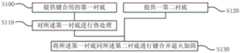
附图1所示是本发明所述半导体衬底的键合方法的一具体实施方式的实施步骤示意图,包括:步骤S100,提供键合用的第一衬底,所述第一衬底为半导体衬底;步骤S110,对所述第一衬底采用第一温度进行热处理;步骤S120,提供一、第二衬底;以及步骤S130,将所述第一衬底同所述第二衬底进行键合并采用第二温度进行退火加固。FIG. 1 is a schematic diagram of the implementation steps of a specific embodiment of the semiconductor substrate bonding method according to the present invention, including: step S100, providing a first substrate for bonding, and the first substrate is a semiconductor substrate bottom; step S110, heat treatment on the first substrate at a first temperature; step S120, providing first and second substrates; and step S130, bonding the first substrate with the second substrate The combination adopts the second temperature for annealing strengthening.
附图2A至附图2D所示是本发明所述半导体衬底的键合方法的具体实施方式的工艺示意图。FIG. 2A to FIG. 2D are schematic process diagrams of specific embodiments of the bonding method of the semiconductor substrate according to the present invention.
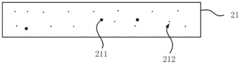
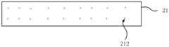
附图2A所示,参考步骤S100,提供键合用的第一衬底21,所述第一衬底21为半导体衬底,且具有氧沉淀211和间隙氧原子212。所示第一衬底21的材料例如可以是单晶硅、单晶锗、锗硅、多晶硅、蓝宝石、SiC、GaAs、以及GaN等任意一种,或者由上述材料构成的多层复合衬底。由于制造工艺问题,第一衬底21中的氧沉淀211天然的分布不均匀,尤其是在单晶硅衬底中表现尤为明显。这些在半导体衬底内部分布不均匀的氧沉淀211在后续的热处理过程中会不断的合并间隙氧原子212而继续长大,并且半导体衬底21内也会有新的间隙氧原子212聚合形成新的氧沉淀211。经仔细研究发现,这些氧沉淀在键合后的热加固环节会带来内部应力的不均匀分布,使键合后的衬底产生严重的翘曲问题,从而影响后续的集成电路制造,比如造成光刻无法对准等问题。As shown in FIG. 2A , referring to step S100 , a
附图2B所示,参考步骤S110,对所述第一衬底21采用第一温度进行热处理。热处理的步骤能够使得氧沉淀211部分或全部地转化成间隙氧原子212。并使得间隙氧原子212在热处理过程中均匀分布。从而在后续的热处理过程中在半导体衬底21整体范围内更加均匀的成核、长大,最终达到抑制衬底翘曲,提升集成电路制造良率的目的。所述键合用半导体衬底为两个,均进行热处理,并彼此键合As shown in FIG. 2B , referring to step S110 , the
上述步骤S110中,为了提高热处理效率,优选的第一温度的温度范围是850℃至1050℃,优选处于第一温度的时间不小于1.5小时,并进一步优选为3小时,优选在含氧气氛中进行。在含氧气氛中进行的热处理,应当在热处理之后去除表面生成的氧化层。In the above step S110, in order to improve the heat treatment efficiency, the preferred temperature range of the first temperature is 850 ° C to 1050 ° C, preferably the time at the first temperature is not less than 1.5 hours, and more preferably 3 hours, preferably in an oxygen-containing atmosphere conduct. For heat treatment in an oxygen-containing atmosphere, the oxide layer formed on the surface should be removed after the heat treatment.
附图2C所示,参考步骤S120,提供一第二衬底22。所述第二衬底22可以是玻璃衬底、半导体衬底或金属衬底。若所述第二衬底22为半导体衬底,优选对其实施类似于步骤S110的热处理工艺。As shown in FIG. 2C, referring to step S120, a
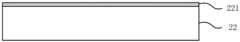
根据需要,本具体实施方式中,衬底22的表面具有绝缘层221,用于在键合后形成业界常见的SOI衬底。在其它的具体实施方式中,绝缘层也可以设置在第一衬底21的表面,或在第一衬底21和第二衬底22的表面同时设置绝缘层;也可以不具有绝缘层,而直接键合。若采用氧化法形成绝缘层,干氧或湿氧均可,氧化温度范围是950℃至1150℃中的大于第一温度且小于第二温度的温度值,并优选其拟用作器件层的半导体衬底进行氧化处理。氧化的过程中,间隙氧小部分变成氧沉淀,间隙氧含量有微量降低,处理温度优选为1000℃-1100℃。According to requirements, in this specific embodiment, the surface of the
附图2D所示,参考步骤S130,将所述第一衬底21同所述第二衬底22进行键合并采用第二温度进行退火加固。优选的第二温度的温度范围是1050℃至1250℃,时间不小于2小时。在退火加固的过程中,间隙氧原子212会合并形成氧沉淀211。而由于步骤S110的热处理步骤改善了间隙氧原子212分布的均匀性,因此本步骤形成的氧沉淀211的分布更均匀,降低了键合后衬底内部由于氧沉淀211的存在而导致的内部应力不均匀。加固后的键合衬底,可以根据需要减薄第一衬底或第二衬底,以获得最终产品。对于上述具体实施方式,应当将经过氧化处理具有绝缘层221的第二衬底22减薄作为最终产品的器件层,而经过多道热处理的第一衬底21作为支撑衬底。As shown in FIG. 2D , referring to step S130 , the
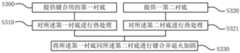
附图3所示是本发明所述半导体衬底的键合方法的又一具体实施方式的实施步骤示意图,包括:步骤S300,提供键合用的第一衬底,所述第一衬底为半导体衬底;步骤S310,对所述第一衬底进行热处理;步骤S320,提供一第二衬底;步骤S321,对所述第二衬底进行热处理,所述第二衬底为半导体衬底;以及步骤S330,将所述第一衬底同所述第二衬底进行键合并退火加固。FIG. 3 is a schematic diagram of the implementation steps of another specific embodiment of the semiconductor substrate bonding method according to the present invention, including: step S300 , providing a first substrate for bonding, and the first substrate is a semiconductor substrate; step S310, heat treatment on the first substrate; step S320, providing a second substrate; step S321, heat treatment on the second substrate, the second substrate being a semiconductor substrate; And step S330, bonding the first substrate and the second substrate and annealing and strengthening.
与前一具体实施方式不同的是,本具体实施方式的第二衬底为半导体衬底,并对其进行热处理,以改善其内部的间隙氧原子的分布状态,使加固后的氧沉淀分布更加均匀,提高键合后衬底的平整度。Different from the previous specific embodiment, the second substrate of this specific embodiment is a semiconductor substrate, and heat treatment is performed on it to improve the distribution state of interstitial oxygen atoms in it, so that the distribution of oxygen precipitation after reinforcement is better. Uniform, improve the flatness of the substrate after bonding.
以上所述仅是本发明的优选实施方式,应当指出,对于本技术领域的普通技术人员,在不脱离本发明原理的前提下,还可以做出若干改进和润饰,这些改进和润饰也应视为本发明的保护范围。The above are only the preferred embodiments of the present invention. It should be pointed out that for those skilled in the art, without departing from the principles of the present invention, several improvements and modifications can also be made, and these improvements and modifications should also be regarded as It is the protection scope of the present invention.
Claims (10)
Translated fromChinesePriority Applications (2)
| Application Number | Priority Date | Filing Date | Title |
|---|---|---|---|
| CN201811124962.2ACN109346433B (en) | 2018-09-26 | 2018-09-26 | Method for bonding semiconductor substrate and bonded semiconductor substrate |
| US16/584,215US11393772B2 (en) | 2018-09-26 | 2019-09-26 | Bonding method for semiconductor substrate, and bonded semiconductor substrate |
Applications Claiming Priority (1)
| Application Number | Priority Date | Filing Date | Title |
|---|---|---|---|
| CN201811124962.2ACN109346433B (en) | 2018-09-26 | 2018-09-26 | Method for bonding semiconductor substrate and bonded semiconductor substrate |
Publications (2)
| Publication Number | Publication Date |
|---|---|
| CN109346433A CN109346433A (en) | 2019-02-15 |
| CN109346433Btrue CN109346433B (en) | 2020-10-23 |
Family
ID=65306999
Family Applications (1)
| Application Number | Title | Priority Date | Filing Date |
|---|---|---|---|
| CN201811124962.2AActiveCN109346433B (en) | 2018-09-26 | 2018-09-26 | Method for bonding semiconductor substrate and bonded semiconductor substrate |
Country Status (2)
| Country | Link |
|---|---|
| US (1) | US11393772B2 (en) |
| CN (1) | CN109346433B (en) |
Families Citing this family (2)
| Publication number | Priority date | Publication date | Assignee | Title |
|---|---|---|---|---|
| US11094536B2 (en)* | 2019-02-28 | 2021-08-17 | Nichia Corporation | Method of manufacturing semiconductor elements |
| CN112466744A (en)* | 2020-11-17 | 2021-03-09 | 深圳宝铭微电子有限公司 | Novel crystal element and preparation method thereof |
Citations (6)
| Publication number | Priority date | Publication date | Assignee | Title |
|---|---|---|---|---|
| CN1256723A (en)* | 1997-04-09 | 2000-06-14 | Memc电子材料有限公司 | Low defect density, ideal oxygen precipitating silicon |
| JP2004119446A (en)* | 2002-09-24 | 2004-04-15 | Shin Etsu Handotai Co Ltd | Annealed wafer and method for manufacturing the same |
| CN1769549A (en)* | 2004-11-05 | 2006-05-10 | 北京有色金属研究总院 | A heat treatment process for single crystal silicon polished sheet |
| CN102605433A (en)* | 2012-01-09 | 2012-07-25 | 浙江大学 | Method for eliminating primary oxygen precipitation in nitrating Czochralski silicon chips |
| CN103144024A (en)* | 2011-12-06 | 2013-06-12 | 有研半导体材料股份有限公司 | Process for manufacturing 300mm silicon polished wafer by using high-temperature heat treatment |
| CN104762656A (en)* | 2014-01-02 | 2015-07-08 | 浙江大学 | Intrinsic gettering technology of major diameter czochralski silicon chip |
Family Cites Families (11)
| Publication number | Priority date | Publication date | Assignee | Title |
|---|---|---|---|---|
| US5593494A (en)* | 1995-03-14 | 1997-01-14 | Memc Electronic Materials, Inc. | Precision controlled precipitation of oxygen in silicon |
| US5994761A (en)* | 1997-02-26 | 1999-11-30 | Memc Electronic Materials Spa | Ideal oxygen precipitating silicon wafers and oxygen out-diffusion-less process therefor |
| MY132874A (en)* | 1997-04-09 | 2007-10-31 | Memc Electronic Materials | Low defect density, vacancy dominated silicon |
| JP2000031439A (en)* | 1998-07-13 | 2000-01-28 | Fuji Electric Co Ltd | SOI substrate and method of manufacturing the same |
| KR100760736B1 (en)* | 2000-01-26 | 2007-09-21 | 신에쯔 한도타이 가부시키가이샤 | Method of manufacturing silicon epitaxial wafer |
| JP2002270800A (en)* | 2001-03-12 | 2002-09-20 | Toyota Motor Corp | Semiconductor device using bonded substrate and method of manufacturing the same |
| WO2006030699A1 (en)* | 2004-09-13 | 2006-03-23 | Shin-Etsu Handotai Co., Ltd. | Soi wafer manufacturing method and soi wafer |
| JP2009176860A (en)* | 2008-01-23 | 2009-08-06 | Sumco Corp | Method for manufacturing bonded wafer |
| CN102130037B (en)* | 2010-12-27 | 2013-03-13 | 上海新傲科技股份有限公司 | Method for preparing semiconductor substrate with insulation buried layer by adopting gettering process |
| CN104766788A (en)* | 2014-01-06 | 2015-07-08 | 无锡华润上华半导体有限公司 | Silicon on insulator and preparation method thereof |
| CN105845548A (en)* | 2015-01-16 | 2016-08-10 | 中芯国际集成电路制造(上海)有限公司 | Silicon substrate and a manufacturing method thereof |
- 2018
- 2018-09-26CNCN201811124962.2Apatent/CN109346433B/enactiveActive
- 2019
- 2019-09-26USUS16/584,215patent/US11393772B2/enactiveActive
Patent Citations (6)
| Publication number | Priority date | Publication date | Assignee | Title |
|---|---|---|---|---|
| CN1256723A (en)* | 1997-04-09 | 2000-06-14 | Memc电子材料有限公司 | Low defect density, ideal oxygen precipitating silicon |
| JP2004119446A (en)* | 2002-09-24 | 2004-04-15 | Shin Etsu Handotai Co Ltd | Annealed wafer and method for manufacturing the same |
| CN1769549A (en)* | 2004-11-05 | 2006-05-10 | 北京有色金属研究总院 | A heat treatment process for single crystal silicon polished sheet |
| CN103144024A (en)* | 2011-12-06 | 2013-06-12 | 有研半导体材料股份有限公司 | Process for manufacturing 300mm silicon polished wafer by using high-temperature heat treatment |
| CN102605433A (en)* | 2012-01-09 | 2012-07-25 | 浙江大学 | Method for eliminating primary oxygen precipitation in nitrating Czochralski silicon chips |
| CN104762656A (en)* | 2014-01-02 | 2015-07-08 | 浙江大学 | Intrinsic gettering technology of major diameter czochralski silicon chip |
Non-Patent Citations (2)
| Title |
|---|
| Oxygen Precipitation Related Stress-Modified Crack Propagation in High Growth Rate Czochralski SiliconWafers;P. K. Kulshreshtha 等;《Journal of The Electrochemical Society》;20111219;第159卷(第2期);第H125-H129页* |
| 硅中氧沉淀的研究;杨德仁;《材料科学与工程》;19900702;第2卷(第2期);第13-19页* |
Also Published As
| Publication number | Publication date |
|---|---|
| CN109346433A (en) | 2019-02-15 |
| US20200098703A1 (en) | 2020-03-26 |
| US11393772B2 (en) | 2022-07-19 |
Similar Documents
| Publication | Publication Date | Title |
|---|---|---|
| CN108493334B (en) | A kind of preparation method of thin film heterostructure | |
| JP7470233B2 (en) | Radio Frequency Silicon-on-Insulator Wafer Platform with Superior Performance, Stability and Manufacturability | |
| US20240022229A1 (en) | Composite substrate | |
| CN113994032B (en) | Substrate for electronic device and method for manufacturing the same | |
| JP5018066B2 (en) | Method for manufacturing strained Si substrate | |
| TWI474397B (en) | Method for forming silicon oxide film of SOI wafer | |
| CN111383915B (en) | Preparation method of heterogeneous bonding structure | |
| CN106711027A (en) | Wafer bonding method and preparation method for foreign substrate | |
| WO2021024654A1 (en) | Substrate for electronic device and production method therefor | |
| CN107195534B (en) | Ge composite substrate, substrate epitaxial structure and preparation method thereof | |
| CN109346433B (en) | Method for bonding semiconductor substrate and bonded semiconductor substrate | |
| JP6288323B2 (en) | Method for producing thermally oxidized heterogeneous composite substrate | |
| JPH0787187B2 (en) | Method for manufacturing GaAs compound semiconductor substrate | |
| CN111383914A (en) | Adjustment method and post-processing method of warpage degree of heterobonded structure | |
| CN118866664A (en) | A method for preparing a silicon epitaxial wafer crack prevention sheet for MOS | |
| JP5710429B2 (en) | Manufacturing method of bonded wafer | |
| US9171737B2 (en) | Thermal oxide film formation method for silicon single crystal wafer | |
| JP5531642B2 (en) | Manufacturing method of bonded wafer | |
| JPH08255882A (en) | Soi substrate and fabrication thereof | |
| CN106601615B (en) | Annealing methods to improve bond strength | |
| JP2001093789A (en) | Method for manufacturing bonded soi wafer | |
| JPS60176241A (en) | Manufacture of semiconductor substrate | |
| JP5575444B2 (en) | Manufacturing method of semiconductor device | |
| JP2011138956A (en) | Method of manufacturing silicon semiconductor substrate | |
| JP2002184699A (en) | Method of treating surface of silicon wafer, and semiconductor wafer |
Legal Events
| Date | Code | Title | Description |
|---|---|---|---|
| PB01 | Publication | ||
| PB01 | Publication | ||
| SE01 | Entry into force of request for substantive examination | ||
| SE01 | Entry into force of request for substantive examination | ||
| GR01 | Patent grant | ||
| GR01 | Patent grant |