CN109301087B - Packaging structure, electronic device and packaging method - Google Patents
Packaging structure, electronic device and packaging methodDownload PDFInfo
- Publication number
- CN109301087B CN109301087BCN201811168204.0ACN201811168204ACN109301087BCN 109301087 BCN109301087 BCN 109301087BCN 201811168204 ACN201811168204 ACN 201811168204ACN 109301087 BCN109301087 BCN 109301087B
- Authority
- CN
- China
- Prior art keywords
- substrate
- sealant
- slope
- distance
- inclined surface
- Prior art date
- Legal status (The legal status is an assumption and is not a legal conclusion. Google has not performed a legal analysis and makes no representation as to the accuracy of the status listed.)
- Active
Links
Images


Classifications
- H—ELECTRICITY
- H10—SEMICONDUCTOR DEVICES; ELECTRIC SOLID-STATE DEVICES NOT OTHERWISE PROVIDED FOR
- H10H—INORGANIC LIGHT-EMITTING SEMICONDUCTOR DEVICES HAVING POTENTIAL BARRIERS
- H10H20/00—Individual inorganic light-emitting semiconductor devices having potential barriers, e.g. light-emitting diodes [LED]
- H10H20/80—Constructional details
- H10H20/85—Packages
- H10H20/852—Encapsulations
- H10H20/853—Encapsulations characterised by their shape
- H—ELECTRICITY
- H10—SEMICONDUCTOR DEVICES; ELECTRIC SOLID-STATE DEVICES NOT OTHERWISE PROVIDED FOR
- H10K—ORGANIC ELECTRIC SOLID-STATE DEVICES
- H10K59/00—Integrated devices, or assemblies of multiple devices, comprising at least one organic light-emitting element covered by group H10K50/00
- H10K59/80—Constructional details
- H10K59/87—Passivation; Containers; Encapsulations
- H10K59/871—Self-supporting sealing arrangements
- H10K59/8722—Peripheral sealing arrangements, e.g. adhesives, sealants
- H—ELECTRICITY
- H10—SEMICONDUCTOR DEVICES; ELECTRIC SOLID-STATE DEVICES NOT OTHERWISE PROVIDED FOR
- H10K—ORGANIC ELECTRIC SOLID-STATE DEVICES
- H10K50/00—Organic light-emitting devices
- H10K50/80—Constructional details
- H10K50/84—Passivation; Containers; Encapsulations
- H10K50/842—Containers
- H10K50/8426—Peripheral sealing arrangements, e.g. adhesives, sealants
- H—ELECTRICITY
- H10—SEMICONDUCTOR DEVICES; ELECTRIC SOLID-STATE DEVICES NOT OTHERWISE PROVIDED FOR
- H10K—ORGANIC ELECTRIC SOLID-STATE DEVICES
- H10K59/00—Integrated devices, or assemblies of multiple devices, comprising at least one organic light-emitting element covered by group H10K50/00
- H10K59/10—OLED displays
- H10K59/12—Active-matrix OLED [AMOLED] displays
- H—ELECTRICITY
- H10—SEMICONDUCTOR DEVICES; ELECTRIC SOLID-STATE DEVICES NOT OTHERWISE PROVIDED FOR
- H10K—ORGANIC ELECTRIC SOLID-STATE DEVICES
- H10K71/00—Manufacture or treatment specially adapted for the organic devices covered by this subclass
- H—ELECTRICITY
- H10—SEMICONDUCTOR DEVICES; ELECTRIC SOLID-STATE DEVICES NOT OTHERWISE PROVIDED FOR
- H10H—INORGANIC LIGHT-EMITTING SEMICONDUCTOR DEVICES HAVING POTENTIAL BARRIERS
- H10H20/00—Individual inorganic light-emitting semiconductor devices having potential barriers, e.g. light-emitting diodes [LED]
- H10H20/01—Manufacture or treatment
- H10H20/036—Manufacture or treatment of packages
- H10H20/0362—Manufacture or treatment of packages of encapsulations
- H—ELECTRICITY
- H10—SEMICONDUCTOR DEVICES; ELECTRIC SOLID-STATE DEVICES NOT OTHERWISE PROVIDED FOR
- H10K—ORGANIC ELECTRIC SOLID-STATE DEVICES
- H10K71/00—Manufacture or treatment specially adapted for the organic devices covered by this subclass
- H10K71/40—Thermal treatment, e.g. annealing in the presence of a solvent vapour
Landscapes
- Engineering & Computer Science (AREA)
- Physics & Mathematics (AREA)
- Optics & Photonics (AREA)
- Manufacturing & Machinery (AREA)
- Microelectronics & Electronic Packaging (AREA)
- Electroluminescent Light Sources (AREA)
Abstract
Translated fromChinese
Description
Translated fromChinese技术领域technical field
本公开至少一实施例涉及一种封装结构、电子装置以及封装方法。At least one embodiment of the present disclosure relates to a packaging structure, an electronic device, and a packaging method.
背景技术Background technique
有些电子器件(例如OLED器件)对抗水汽和氧气的能力较差,如果暴露在水汽或氧气中,这些电子器件的寿命会减小。对于电子器件的封装,目前的封装技术包括采用密封胶和封装盖板进行封装以及薄膜封装技术等,实现好的封装效果对提高电子器件的使用寿命具有重要意义。Some electronic devices, such as OLED devices, are less resistant to water vapor and oxygen, and if exposed to water vapor or oxygen, the lifetime of these electronic devices is reduced. For the packaging of electronic devices, the current packaging technologies include encapsulation using sealants and packaging cover plates, and thin-film packaging technologies. Achieving a good packaging effect is of great significance to improving the service life of electronic devices.
发明内容SUMMARY OF THE INVENTION
本公开至少一实施例提供一种封装结构,该封装结构包括:第一基板、第二基板、第一密封胶和第二密封胶。第二基板与所述第一基板相对设置;第一密封胶和第二密封胶设置于所述第一基板和所述第二基板之间并使所述第一基板和所述第二基板相互接合;所述第一密封胶包括远离所述第一基板的第一斜面;所述第二密封胶包括远离所述第二基板的第二斜面,所述第二斜面与所述第一斜面贴合;在平行于所述第一基板和所述第二基板的方向上,所述第一斜面和所述第二斜面从第一位置延伸到第二位置,沿从所述第一位置到所述第二位置的方向,所述第一斜面到所述第一基板的距离逐渐变化,所述第二斜面到所述第二基板的距离逐渐变化;并且,在从所述第一位置到所述第二位置的范围内,所述第一斜面到所述第一基板的距离与所述第二斜面到所述第二基板的距离之和基本相等。At least one embodiment of the present disclosure provides a package structure including: a first substrate, a second substrate, a first sealant, and a second sealant. The second substrate is arranged opposite to the first substrate; the first sealant and the second sealant are arranged between the first substrate and the second substrate and make the first substrate and the second substrate mutually bonding; the first sealant includes a first slope away from the first substrate; the second sealant includes a second slope away from the second substrate, and the second slope is attached to the first slope combined; in a direction parallel to the first substrate and the second substrate, the first inclined plane and the second inclined plane extend from the first position to the second position, along the direction from the first position to the second position In the direction of the second position, the distance from the first slope to the first substrate gradually changes, and the distance from the second slope to the second substrate gradually changes; Within the range of the second position, the sum of the distance from the first slope to the first substrate and the distance from the second slope to the second substrate is substantially equal.
例如,本公开至少一实施例提供的封装结构中,沿从所述第一位置到所述第二位置的方向,所述第一斜面到所述第一基板的距离逐渐减小,所述第二斜面到所述第二基板的距离逐渐增大。For example, in the package structure provided by at least one embodiment of the present disclosure, along the direction from the first position to the second position, the distance from the first slope to the first substrate gradually decreases, and the first slope gradually decreases. The distance from the two slopes to the second substrate gradually increases.
例如,本公开至少一实施例提供的封装结构中,沿从所述第一位置到所述第二位置的方向,所述第一斜面到所述第一基板的距离逐渐增大,所述第二斜面到所述第二基板的距离逐渐减小。For example, in the package structure provided by at least one embodiment of the present disclosure, along the direction from the first position to the second position, the distance from the first slope to the first substrate gradually increases, and the first slope gradually increases. The distance from the two slopes to the second substrate gradually decreases.
例如,本公开至少一实施例提供的封装结构中,所述第一斜面与所述第一基板所在平面之间具有第一夹角,所述第二斜面与所述第二基板所在平面之间具有第二夹角;所述第一夹角与所述第二夹角相等。For example, in the package structure provided by at least one embodiment of the present disclosure, there is a first included angle between the first inclined surface and the plane where the first substrate is located, and between the second inclined surface and the plane where the second substrate is located There is a second included angle; the first included angle is equal to the second included angle.
例如,本公开至少一实施例提供的封装结构中,所述第一斜面在所述第一基板上的正投影与所述第二斜面在所述第一基板上的正投影基本重合。For example, in the package structure provided by at least one embodiment of the present disclosure, the orthographic projection of the first slope on the first substrate substantially coincides with the orthographic projection of the second slope on the first substrate.
例如,本公开至少一实施例提供的封装结构中,所述第一密封胶的平面形状包括多个第一条形,所述多个第一条形中的每一个包括所述第一斜面;所述第二密封胶的平面形状包括多个第二条形,所述多个第二条形中的每一个包括所述第二斜面。For example, in the package structure provided by at least one embodiment of the present disclosure, the planar shape of the first sealant includes a plurality of first strips, and each of the plurality of first strips includes the first slope; The planar shape of the second sealant includes a plurality of second strips, and each of the plurality of second strips includes the second slope.
例如,本公开至少一实施例提供的封装结构中,所述多个第一条形构成封闭的环形,所述多个第二条形构成封闭的环形。For example, in the package structure provided by at least one embodiment of the present disclosure, the plurality of first strip shapes form a closed loop, and the plurality of second strip shapes form a closed loop.
例如,本公开至少一实施例提供的封装结构中,所述第一密封胶和所述第二密封胶的材料为紫外光固化型树脂或热固化型树脂。For example, in the package structure provided by at least one embodiment of the present disclosure, the materials of the first sealant and the second sealant are UV-curable resin or heat-curable resin.
本公开至少一实施例还提供的一种电子装置,该电子装置包括本公开实施例提供的任意一种封装结构。At least one embodiment of the present disclosure further provides an electronic device, where the electronic device includes any one of the packaging structures provided by the embodiments of the present disclosure.
本公开至少一实施例还提供的一种封装方法,该封装方法包括:提供第一基板和第二基板;在所述第一基板上和所述第二基板之间形成第一密封胶和第二密封胶,其中,所述第一密封胶包括远离所述第一基板的第一斜面,所述第二密封胶包括远离所述第二基板的第二斜面;以及采用所述第一密封胶和所述第二密封胶将所述第一基板和所述第二基板彼此接合;所述第二斜面与所述第一斜面贴合;在平行于所述第一基板和所述第二基板的方向上,所述第一斜面和所述第二斜面从第一位置延伸到第二位置,沿从所述第一位置到所述第二位置的方向,所述第一斜面到所述第一基板的距离逐渐变化,所述第二斜面到所述第二基板的距离逐渐变化;并且,在从所述第一位置到所述第二位置的范围内,所述第一斜面到所述第一基板的距离与所述第二斜面到所述第二基板的距离之和基本相等。At least one embodiment of the present disclosure further provides a packaging method, the packaging method includes: providing a first substrate and a second substrate; forming a first sealant and a second substrate on the first substrate and between the second substrate Two sealants, wherein the first sealant includes a first slope away from the first substrate, the second sealant includes a second slope away from the second substrate; and the first sealant is used and the second sealant to bond the first substrate and the second substrate to each other; the second inclined surface is attached to the first inclined surface; parallel to the first substrate and the second substrate The first inclined plane and the second inclined plane extend from the first position to the second position in the direction of The distance of a substrate changes gradually, and the distance from the second slope to the second substrate changes gradually; and, in the range from the first position to the second position, the first slope to the The distance from the first substrate is substantially equal to the sum of the distances from the second inclined surface to the second substrate.
例如,本公开至少一实施例提供的封装方法中,在所述第一基板上形成所述第一密封胶,在所述第二基板上形成所述第二密封胶;沿两个彼此相反的方向分别涂覆形成所述第一密封胶与所述第二密封胶。For example, in the packaging method provided by at least one embodiment of the present disclosure, the first sealant is formed on the first substrate, and the second sealant is formed on the second substrate; The first sealant and the second sealant are formed by coating in the directions respectively.
例如,本公开至少一实施例提供的封装方法中,在所述第一基板上沿从所述第一位置到所述第二位置的方向涂覆所述第一密封胶,在从所述第一位置到所述第二位置的范围内,所述第一斜面到所述第一基板上的距离逐渐减小;在所述第二基板上沿与从所述第二位置到所述第一位置的方向涂覆所述第二密封胶,在从所述第一位置到所述第二位置的范围内,所述第二斜面到所述第二基板的距离逐渐增大。For example, in the packaging method provided by at least one embodiment of the present disclosure, the first sealant is coated on the first substrate in a direction from the first position to the second position, and the first sealant is applied from the first position to the second position. In the range from a position to the second position, the distance from the first slope to the first substrate gradually decreases; on the second substrate the distance from the second position to the first The second sealant is applied in the direction of the position, and in the range from the first position to the second position, the distance from the second slope to the second substrate gradually increases.
例如,本公开至少一实施例提供的封装方法中,在所述第一基板上沿从所述第二位置到所述第一位置的方向涂覆所述第一密封胶,在从所述第一位置到所述第二位置的范围内,所述第一斜面到所述第一基板上的距离逐渐增大;在所述第二基板上沿从所述第一位置到所述第二位置的方向涂覆所述第二密封胶,在从所述第一位置到所述第二位置的范围内,所述第二斜面到所述第二基板的距离逐渐减小。For example, in the packaging method provided by at least one embodiment of the present disclosure, the first sealant is coated on the first substrate in a direction from the second position to the first position, and the first sealant is applied from the second position to the first position. Within the range from a position to the second position, the distance from the first inclined plane to the first substrate gradually increases; on the second substrate the distance from the first position to the second position increases gradually. The second sealant is applied in the direction of the first position, and the distance from the second slope to the second substrate gradually decreases in the range from the first position to the second position.
例如,本公开至少一实施例提供的封装方法中,所述第一斜面与所述第一基板所在平面之间具有第一夹角,所述第二斜面与所述第二基板所在平面之间具有第二夹角;所述第一夹角与所述第二夹角相等。For example, in the packaging method provided by at least one embodiment of the present disclosure, there is a first included angle between the first inclined surface and the plane where the first substrate is located, and the second inclined surface and the plane where the second substrate is located. There is a second included angle; the first included angle is equal to the second included angle.
例如,本公开至少一实施例提供的封装方法中,所述第一斜面在所述第一基板上的正投影与所述第二斜面在所述第一基板上的正投影基本重合。For example, in the packaging method provided by at least one embodiment of the present disclosure, the orthographic projection of the first slope on the first substrate substantially coincides with the orthographic projection of the second slope on the first substrate.
例如,本公开至少一实施例提供的封装方法中,所述第一密封胶的平面形状包括多个第一条形,所述多个第一条形中的每一个包括所述第一斜面;所述第二密封胶的平面形状包括多个第二条形,所述多个第二条形中的每一个包括所述第二斜面。For example, in the packaging method provided by at least one embodiment of the present disclosure, the planar shape of the first sealant includes a plurality of first strip shapes, and each of the plurality of first strip shapes includes the first slope; The planar shape of the second sealant includes a plurality of second strips, and each of the plurality of second strips includes the second slope.
例如,本公开至少一实施例提供的封装方法中,所述多个第一条形构成封闭的环形,所述多个第二条形构成封闭的环形。For example, in the packaging method provided by at least one embodiment of the present disclosure, the plurality of first strip shapes form a closed loop, and the plurality of second strip shapes form a closed loop.
例如,本公开至少一实施例提供的封装方法中,在将所述第一基板和所述第二基板彼此接合之前,所述封装方法还包括:对所述第一密封胶和所述第二密封胶进行部分固化以使所述第一密封胶和所述第二密封胶不能流动。For example, in the packaging method provided by at least one embodiment of the present disclosure, before bonding the first substrate and the second substrate to each other, the packaging method further includes: applying the first sealant and the second substrate to each other. The sealant is partially cured so that the first sealant and the second sealant cannot flow.
例如,本公开至少一实施例提供的封装方法中,在将所述第一基板和所述第二基板彼此接合之后,所述封装方法还包括对所述第一密封胶和所述第二密封胶进行固化。For example, in the packaging method provided by at least one embodiment of the present disclosure, after the first substrate and the second substrate are bonded to each other, the packaging method further includes sealing the first sealant and the second sealant. glue to cure.
附图说明Description of drawings
为了更清楚地说明本发明实施例的技术方案,下面将对实施例的附图作简单地介绍,显而易见地,下面描述中的附图仅仅涉及本发明的一些实施例,而非对本发明的限制。In order to illustrate the technical solutions of the embodiments of the present invention more clearly, the accompanying drawings of the embodiments will be briefly introduced below. Obviously, the drawings in the following description only relate to some embodiments of the present invention, rather than limit the present invention. .
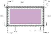
图1为本公开一实施例提供的一种封装结构的平面示意图;FIG. 1 is a schematic plan view of a package structure according to an embodiment of the present disclosure;
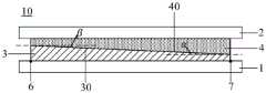
图2A为沿图1中的A-A’线的一种剖面示意图;Fig. 2 A is a kind of sectional schematic diagram along the line A-A' in Fig. 1;
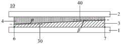
图2B为沿图1中的A-A’线的另一种剖面示意图;Fig. 2B is another kind of sectional schematic diagram along the line A-A' in Fig. 1;
图3为本公开一实施例提供的一种电子装置示意图;FIG. 3 is a schematic diagram of an electronic device according to an embodiment of the present disclosure;
图4A-4F为本公开一实施例提供的一种封装方法示意图;4A-4F are schematic diagrams of a packaging method according to an embodiment of the present disclosure;
图5A-5F为本公开一实施例提供的一种封装方法示意图。5A-5F are schematic diagrams of a packaging method according to an embodiment of the present disclosure.
附图标记reference number
1-第一基板;2-第二基板;3-第一密封胶;30-第一斜面;31/32/33/34-第一条形;4-第二密封胶;40-第二斜面;41/42/43/44-第二条形;5-电子器件;6/61/62/63/64-第一位置;7/71/72/73/74-第二位置;10-封装结构;11-电子装置。1-first substrate; 2-second substrate; 3-first sealant; 30-first bevel; 31/32/33/34-first strip; 4-second sealant; 40-second bevel ; 41/42/43/44 - second bar; 5 - electronics; 6/61/62/63/64 - first position; 7/71/72/73/74 - second position; 10 - package Structure; 11-Electronics.
具体实施方式Detailed ways
为使本发明实施例的目的、技术方案和优点更加清楚,下面将结合本发明实施例的附图,对本发明实施例的技术方案进行清楚、完整地描述。显然,所描述的实施例是本发明的一部分实施例,而不是全部的实施例。基于所描述的本发明的实施例,本领域普通技术人员在无需创造性劳动的前提下所获得的所有其它实施例,都属于本发明保护的范围。In order to make the purpose, technical solutions and advantages of the embodiments of the present invention clearer, the technical solutions of the embodiments of the present invention will be clearly and completely described below with reference to the accompanying drawings of the embodiments of the present invention. Obviously, the described embodiments are some, but not all, embodiments of the present invention. Based on the described embodiments of the present invention, all other embodiments obtained by those of ordinary skill in the art without creative efforts fall within the protection scope of the present invention.
除非另作定义,此处使用的技术术语或者科学术语应当为本发明所属领域内具有一般技能的人士所理解的通常意义。本发明专利申请说明书以及权利要求书中使用的“第一”、“第二”以及类似的词语并不表示任何顺序、数量或者重要性,而只是用来区分不同的组成部分。“包括”或者“包含”等类似的词语意指出现在该词前面的元件或者物件涵盖出现在该词后面列举的元件或者物件及其等同,而不排除其他元件或者物件。“内”、“外”、“上”、“下”等仅用于表示相对位置关系,当被描述对象的绝对位置改变后,则该相对位置关系也可能相应地改变。Unless otherwise defined, technical or scientific terms used herein should have the ordinary meaning as understood by one of ordinary skill in the art to which this invention belongs. The terms "first", "second" and similar terms used in the description of the patent application and the claims of the present invention do not denote any order, quantity or importance, but are only used to distinguish different components. "Comprising" or "comprising" and similar words mean that the elements or things appearing before the word encompass the elements or things recited after the word and their equivalents, but do not exclude other elements or things. "Inner", "outer", "upper", "lower", etc. are only used to indicate the relative positional relationship, and when the absolute position of the described object changes, the relative positional relationship may also change accordingly.
本公开所使用的附图并不是严格按实际比例绘制,各个结构的具体地尺寸和数量可根据实际需要进行确定。本公开中所描述的附图仅是结构示意图。The drawings used in the present disclosure are not drawn strictly in actual scale, and the specific size and quantity of each structure can be determined according to actual needs. The drawings described in the present disclosure are only schematic structural diagrams.
目前,在利用封装盖板和密封胶对电子器件进行密封的过程中,在基板(例如为设置有电子器件的衬底基板或者封装盖板)上涂覆密封胶时(此处以在设置有电子器件的衬底基板上涂覆密封胶为例),通常沿一个方向进行涂覆,由于涂覆工艺本身的原因,密封胶在垂直于基板方向上的高度会沿涂覆方向逐渐减少,导致密封胶与封装盖板之间存在间隙,从而封装结构易发生漏气等不良。或者,封装盖板发生倾斜,封装盖板与衬底基板不平行,从而影响封装结构的性能。At present, in the process of sealing the electronic device with the package cover plate and the sealant, when the sealant is applied on the substrate (for example, the base substrate provided with the electronic device or the package cover plate) The sealant is applied on the substrate substrate of the device as an example), which is usually applied in one direction. Due to the coating process itself, the height of the sealant in the direction perpendicular to the substrate will gradually decrease along the coating direction, resulting in sealing There is a gap between the glue and the package cover, so that the package structure is prone to air leakage and other defects. Or, the package cover plate is inclined, and the package cover plate is not parallel to the base substrate, thereby affecting the performance of the package structure.
图1为本公开一实施例提供的一种封装结构的平面示意图,图2A为沿图1中的A-A’线的一种剖面示意图。如图1和图2A所示,该封装结构10可以实现对电子器件5的密封,封装结构10包括第一基板1、第二基板2、第一密封胶3和第二密封胶4。电子器件5位于第一基板1和第二基板2之间,第一密封胶3和第二密封胶4设置于电子器件5的外侧(即,电子器件5的靠近第一基板1和第二基板2的边缘的一侧),并围绕电子器件5设置,以对电子器件5进行密封。如图2A所示,第二基板2与第一基板1相对设置;第一密封胶3和第二密封胶4设置于第一基板1和第二基板2之间并使第一基板1和第二基板2相互接合。第一密封胶3包括远离第一基板1的第一斜面30,第二密封胶4包括远离第二基板2的第二斜面40,第二斜面40与第一斜面30贴合。例如。第一基板1与第二基板2平行。例如,在平行于第一基板1和第二基板2的方向上,第一斜面30和第二斜面40从第一位置6延伸到第二位置7。沿从第一位置6到第二位置7的方向,第一斜面30到第一基板1的距离逐渐变化,第二斜面40到第二基板2的距离逐渐变化。在从第一位置6到第二位置7的范围内,第一斜面30到第一基板1的距离h1与第二斜面40到第二基板2的距离h2之和基本相等,即在垂直于第一基板1和第二基板2的方向上,第一密封胶3和第二密封胶4的厚度之和基本相等,以使得在从第一位置6到第二位置7的范围内,由第一密封胶3和第二密封胶4构成的密封胶具有均匀的厚度,防止由于密封胶的厚度不均匀造成在密封胶与基板之间出现空隙,提高密封的严密性,从而防止外界的湿气、氧气等通过该空隙进入封装结构内部而接触到电子器件5,以延长电子器件5的使用寿命。同时,防止由于密封胶的厚度不均匀造成第一基板1和第二基板2不平行,即防止封装结构10的第二基板2相对于第一基板1倾斜,从而影响该封装结构10的性能以及利用该封装结构10的电子装置(例如显示装置)的性能。FIG. 1 is a schematic plan view of a package structure according to an embodiment of the disclosure, and FIG. 2A is a schematic cross-sectional view along line AA' in FIG. 1 . As shown in FIG. 1 and FIG. 2A , the
需要说明的是,在形成第一斜面30和第二斜面40的制作工艺中,由于不可避免的工艺误差所造成的在从第一位置6到第二位置7的范围内,第一斜面30到第一基板1的距离h1与第二斜面40到第二基板2的距离h2误差之和存在不完全相等的情况(例如h1和h2的工艺误差在±3%以内)包含在本公开的方案之中。It should be noted that, in the manufacturing process of forming the first
例如,第一密封胶3和第二密封胶4的材料为紫外光固化型树脂,例如可以是自由基紫外光固化树脂(环氧丙烯酸树脂、聚氨酯丙烯酸树脂或聚酯丙烯酸树脂等),也可以为阳离子型光固化树脂(环氧树脂或乙烯基醚树脂等)。例如,第一密封胶3和第二密封胶4也可以是热固化型封装胶,例如加成型有机硅胶。当然,第一密封胶3和第二密封胶4不限于以上所列举的种类。例如,第一密封胶3的材料和第二密封胶4的材料相同。例如,第一密封胶3的材料和第二密封胶4的材料不同。For example, the materials of the
例如,本公开实施例中的电子器件5可以包括一个或多个电致发光器件,电致发光器件例如包括有机发光二极管器件或无机电致发光器件。例如,电子器件5包括一个或多个有机发光二极管器件。例如,该多个有机发光二极管器件呈阵列排布,整体上形成一个面状的结构,可以应用于需要整面发光的装置。每个有机发光二极管器件例如包括依次层叠的阳极、有机发光层、阴极,在工作时,电子从阴极注入,空穴从阳极注入,二者在有机发光层中复合,然后激发发光。根据需要,从阳极到有机发光层还可以设置空穴注入层、空穴传输层,从阴极到有机发光层还可以设置电子注入层、电子传输层。例如,阳极通常采用高功函数的导电材料,例如铟锡氧化物(ITO)等;阴极通常采用低功函数的导电材料,例如Ag、Al、Ca、In、Li与Mg等金属,或低功函数的复合金属(例如Mg-Ag镁银)等。有机发光二极管器件在工作时可以发出例如红光、绿光、蓝光,也可以发出白光等;例如,为了辅助调整光的颜色,在有机发光二极管器件出光侧还可以设置荧光层或滤色片等结构。For example, the
在本公开实施例提供的封装结构10中,例如,第一基板1可以为衬底基板,第二基板2为封装盖板。例如,衬底基板包括电子器件5和用于驱动电子器件5的驱动电路,例如包括电源线等,例如还可以包括栅线、数据线、开关晶体管、驱动晶体管、存储电容等。例如,第一基板1和第二基板2可以为石英基板、玻璃基板或塑料基板等。当然,第一基板1和第二基板2类型和材料不限于上述列举种类,本公开实施例对此不作限定。In the
例如,本公开的一个实施例中,如图2A所示,沿从第一位置6到第二位置7的方向,第一斜面30到第一基板1的距离h1逐渐减小,第二斜面40到第二基板2的距离h2逐渐增大,以使得h1与h2之和基本相等,从而达到上述技术效果。For example, in an embodiment of the present disclosure, as shown in FIG. 2A , along the direction from the
例如,第一斜面30与第一基板1所在平面之间具有第一夹角α,第二斜面40与第二基板2所在平面之间具有第二夹角β;第一夹角α与第二夹角β相等,以保证第一基板1与第二基板2平行,从而避免第二基板2或第一基板1发生倾斜而带来的不良。For example, there is a first included angle α between the first
例如,第一斜面30在第一基板1上的正投影与第二斜面40在第一基板1上的正投影基本重合。如此,第一斜面30和第二斜面40完全对合,使得第一密封胶3在垂直于第一基板1方向上的厚度和第二密封胶4在垂直于第一基板1方向上的厚度都能够彼此互补,以获得更好的密封性以及保证第一基板1与第二基板2平行。For example, the orthographic projection of the first
需要说明的是,在将第一斜面30和第二斜面40贴合时的对准过程中,由于不可避免的工艺误差所造成的第一斜面30在第一基板1上的正投影与第二斜面40在第一基板1上的正投影不完全重合的情况(例如对准误差在±3%)以内包含在本公开的方案之中。It should be noted that, during the alignment process when the first
例如,如图1所示,第一密封胶3的平面形状包括多个第一条形31/32/33/34,多个第一条形31/32/33/34中的每一个包括所述第一斜面30;相应地,第二密封胶4的平面形状包括多个第二条形41/42/43/44,多个第二条形41/42/43/44中的每一个包括所述第二斜面40。也就是说,沿图1中的B-B’线、C-C’线、D-D’线的剖面图均如图2A所示。如此,能够在多个位置均能够利用第一密封胶1和第二密封胶2的厚度互补而使的密封胶(由第一密封胶1和第二密封胶2构成)具有相等的厚度,在多个位置避免密封胶与第一基板1或第二基板2之间具有空隙,实现更好的密封效果。For example, as shown in FIG. 1 , the planar shape of the
例如,多个第一条形31/32/33/34构成封闭的环形,多个第二条形41/42/43/44构成封闭的环形。从而,多个第一条形31/32/33/34和多个第二条形41/42/43/44构成围绕电子器件5的封闭的环。如此,在围绕电子器件5的各个位置均能够使密封胶具有相等的厚度而避免密封胶与第一基板1或第二基板2之间具有空隙,实现更好的密封效果。For example, the plurality of
例如,图2B为沿图1中的A-A’线的另一种剖面示意图。图2B所示的实施例与图2A所示的实施例的区别在于,在图2B中,沿从第一位置6到第二位置7的方向,第一斜面30到第一基板1的距离h1逐渐增大,第二斜面40到第二基板2的距离h2逐渐减小,以使得h1与h2之和基本相等,从而达到上述技术效果。图2B所示的实施例的其他特征均与图2A所示的实施例的相同,请参考之前的描述,在此不再赘述。For example, FIG. 2B is another schematic cross-sectional view along the line AA' in FIG. 1 . The difference between the embodiment shown in FIG. 2B and the embodiment shown in FIG. 2A is that, in FIG. 2B , in the direction from the
本实施例提供的有封装结构可以应用于例如显示装置、照明装置(例如照明用的灯)等。The package structure provided in this embodiment can be applied to, for example, a display device, a lighting device (eg, a lamp for lighting), and the like.
本公开至少一实施例还提供的一种电子装置,该电子装置包括本公开实施例提供的任意一种封装结构。At least one embodiment of the present disclosure further provides an electronic device, where the electronic device includes any one of the packaging structures provided by the embodiments of the present disclosure.
图3为本公开一实施例提供的一种电子装置示意图。例如,如图3所示,本公开至少一实施例还提供的一种电子装置11,该电子装置11包括本公开实施例提供的任意一种封装结构10。该电子装置11具有较好的密封性和较长的使用寿命,并且,该电子装置的第一基板和第二基板彼此具有较好的平行度,使电子器件具有较好的性能,避免第一基板或第二基板发生倾斜导致的缺陷(例如电子装置11为显示装置时导致的显示缺陷)。FIG. 3 is a schematic diagram of an electronic device according to an embodiment of the present disclosure. For example, as shown in FIG. 3 , at least one embodiment of the present disclosure further provides an
例如,电子装置11可以为显示装置(例如OLED显示装置、无机电致发光显示装置等),例如电子装置11可以是手机、平板电脑、电视机、显示器、笔记本电脑、数码相机、导航仪等具有显示功能的产品或部件。例如,电子装置11也可以是照明装置(例如OLED照明装置等),例如,照明灯具、装饰性彩灯等。当然,本公开实施例对电子装置的种类没有限定。For example, the
需要说明的是,图3只是包括本公开实施例提供的任意一种封装结构的电子装置的示意图,电子装置的未示出的其他结构,本领域技术人员可参考常规技术,本实施例对此不作限定。It should be noted that FIG. 3 is only a schematic diagram of an electronic device including any one of the packaging structures provided in the embodiments of the present disclosure. For other structures of the electronic device that are not shown, those skilled in the art may refer to conventional techniques. Not limited.
本公开至少一实施例还提供的一种封装方法,该封装方法包括:提供第一基板和第二基板;在所述第一基板上和所述第二基板之间形成第一密封胶和第二密封胶,其中,所述第一密封胶包括远离所述第一基板的第一斜面,所述第二密封胶包括远离所述第二基板的第二斜面;以及采用所述第一密封胶和所述第二密封胶将所述第一基板和所述第二基板彼此接合;所述第二斜面与所述第一斜面贴合;在平行于所述第一基板和所述第二基板的方向上,所述第一斜面和所述第二斜面从第一位置延伸到第二位置,沿从所述第一位置到所述第二位的方向,所述第一斜面到所述第一基板的距离逐渐变化,所述第二斜面到所述第二基板的距离逐渐变化;并且,在从所述第一位置到所述第二位置的范围内,所述第一斜面到所述第一基板的距离与所述第二斜面到所述第二基板的距离之和基本相等。At least one embodiment of the present disclosure further provides a packaging method, the packaging method includes: providing a first substrate and a second substrate; forming a first sealant and a second substrate on the first substrate and between the second substrate Two sealants, wherein the first sealant includes a first slope away from the first substrate, the second sealant includes a second slope away from the second substrate; and the first sealant is used and the second sealant to bond the first substrate and the second substrate to each other; the second inclined surface is attached to the first inclined surface; parallel to the first substrate and the second substrate The first slope and the second slope extend from the first position to the second position in the direction of The distance of a substrate changes gradually, and the distance from the second slope to the second substrate changes gradually; and, in the range from the first position to the second position, the first slope to the The distance from the first substrate is substantially equal to the sum of the distances from the second inclined surface to the second substrate.
例如,在第一基板上形成第一密封胶,在第二基板上形成第二密封胶。例如,沿两个彼此相反的方向分别涂覆形成第一密封胶与第二密封胶。For example, the first sealant is formed on the first substrate and the second sealant is formed on the second substrate. For example, the first sealant and the second sealant are respectively formed by coating in two opposite directions.
示范性地,图4A-4F为本公开一实施例提供的一种封装方法示意图,图4B为形成图4A所示的第一密封胶后的第一基板的平面示意图,图4D为形成图4C所示的第二密封胶后的第二基板的平面示意图。Exemplarily, FIGS. 4A-4F are schematic diagrams of a packaging method according to an embodiment of the present disclosure, FIG. 4B is a schematic plan view of a first substrate after forming the first sealant shown in FIG. 4A , and FIG. 4D is a schematic diagram of forming FIG. 4C . A schematic plan view of the second substrate after the second sealant is shown.
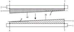
如图4A和4B所示,提供第一基板1,在第一基板1上形成电子器件5。例如,可采用半导体工艺形成电子器件5。本领技术人员可参考本领域常规技术形成电子器件5。例如,在第一基板1上电子器件5的外侧(即,电子器件5靠近第一基板1的边缘的一侧)形成第一密封胶3。例如,采用涂覆的方式形成第一密封胶3。例如,在第一基板1上沿从第一位置6到第二位置7的方向(即图4A中的箭头方向)涂覆第一密封胶3。例如,采用涂覆装置涂覆第一密封胶3,位于涂覆装置的密封胶出口位置的刮刀沿从第一位置6到第二位置7的方向运动,刮刀会经过已经形被涂覆的第一密封胶3的远离第一基板1的表面,而使第一密封胶3在垂直于第一基板1方向上的厚度沿刮刀的运动方向逐渐减少。从而,第一密封胶3包括远离第一基板1的第一斜面30,并且,在从第一位置6到第二位置7的方向上,第一斜面30到第一基板1上的距离h1(即第一密封胶3在垂直于第一基板1方向上的厚度)逐渐减小,第一斜面30与第一基板1所在平面之间具有第一夹角α。As shown in FIGS. 4A and 4B , a
例如,如图4B所示,第一密封胶3的平面形状包括多个第一条形31/32/33/34,多个第一条形31/32/33/34中的每一个包括所述第一斜面30。上述形成第一密封胶3的方法为形成多个第一条形31/32/33/34中的一个,分别采用上述形成第一密封胶3的方法依次形成多个第一条形31/32/33/34。例如,按逆时针依次形成第一条形31、第一条形32、第一条形33和第一条形34。上述第一位置和第二位置是相对于多个条形31/32/33/34中的每一个而存在的。例如,形成第一条形31时,沿从第一位置61到第二位置71的方向涂覆形成第一条形31;形成第一条形32时,沿从第一位置62到第二位置72的方向涂覆形成第一条形32;形成第一条形33时,沿从第一位置63到第二位置73的方向涂覆形成第一条形33;形成第一条形34时,沿从第一位置64到第二位置74的方向涂覆形成第一条形34。例如,多个第一条形31/32/33/34构成封闭的环形,该封闭的环形位于电子器件5的外侧并围绕电子器件5。For example, as shown in FIG. 4B , the planar shape of the
如图4C所示,提供第二基板2,在第二基板2上与第一密封胶3对应的位置形成第二密封胶4,以使后续将第一基板1与第二基板对合后,第一密封胶3能够与第二密封胶4贴合。在第二基板2上沿从第二位置7到第一位置6的方向(即图4C中的箭头方向)涂覆第二密封胶4。在后续将第一基板1与第二基板2对合后,图4C中的第一位置6和图4A中的第一位置6重合,图4C中的第二位置7和图4A中的第二位置7重合。例如,采用涂覆装置涂覆第二密封胶4,位于涂覆装置的密封胶出口位置的刮刀沿从第二位置7到第一位置6的方向运动,刮刀会经过已经形被涂覆的第二密封胶4的远离第二基板2的表面,而使第二密封胶4在垂直于第二基板2方向上的厚度沿刮刀的运动方向逐渐减少。从而,第二密封胶4包括远离第二基板2的第二斜面40,并且,在从第二位置7到第一位置6的方向上,第二斜面40到第二基板2上的距离h2(即第二密封胶4在垂直于第二基板2方向上的厚度)逐渐减小,即,在从第一位置6到第二位置7的方向上,第二斜面40到第二基板2的距离h2逐渐增大。第二斜面40与第二基板2所在平面之间具有第二夹角β。例如,第一夹角α与第二夹角β相等。需要说明的是,在形成第一夹角α和第二夹角β的过程中,由于不可避免的工艺误差所造成的第一夹角α和第二夹角β不完全相等的情况(例如制作工艺误差在±3%)以内包含在本公开的方案之中。As shown in FIG. 4C , a
例如,如图4D所示,第二密封胶4的平面形状包括多个第二条形41/42/43/44,多个第二条形41/42/43/44中的每一个包括所述第二斜面40。上述形成第二密封胶4的方法为形成多个第二条形41/42/43/44中的一个,分别采用上述形成第二密封胶4的方法依次形成多个第二条形41/42/43/44。例如,按顺时针依次形成第二条形41、第二条形42、第二条形43和第二条形44。上述第一位置和第二位置是相对于多个第二条形41/42/43/44中的每一个而存在的。例如,形成第二条形41时,沿从第二位置71到第一位置61的方向涂覆形成第二条形41;形成第二条形42时,沿从第二位置72到第一位置62的方向涂覆形成第二条形42;形成第二条形43时,沿从第二位置73到第一位置63的方向涂覆形成第二条形43;形成第二条形44时,沿从第二位置74到第一位置64的方向涂覆形成第二条形44。例如,多个第二条形41/42/43/44构成封闭的环形,该封闭的环形与图4B中由多个第一条形31/32/33/34构成的封闭的环形相对于,以使后续将第一基板1与第二基板2对合(彼此接合)后,第一密封胶3能够与第二密封胶4贴合。For example, as shown in FIG. 4D, the planar shape of the
例如,在将第一基板1和第二基板2彼此接合之前,封装方法还包括:对第一密封胶3和第二密封胶4进行部分固化以使第一密封胶3和第二密封胶4不能流动。即对图4A中的第二密封胶4和图4C中的第二密封胶4进行部分固化以使第一密封胶2和第二密封胶4不能流动,以防止将第一基板1和第二基板2对合的过程中,第一密封胶3和第二密封胶4发生变形。部分固化后的第一密封胶2和第二密封胶4不能流动,所以形状不会因流动发生改变,其与完全固化后的密封胶不同,其仍然具有粘结性能。具体的部分固化方法可根据第一密封胶2和第二密封胶4的材料进行选择。例如,当第一密封胶2和第二密封胶4的材料为紫外光固化树脂时,可采用紫外光照射的方法进行部分固化,调节紫外光的强度和光照时间,实现对第一密封胶2和第二密封胶4的部分固化。例如,当第一密封胶2和第二密封胶4的材料为热固化树脂时,可采用加热的方法进行部分固化,调节加热的温度和加热时间,实现对第一密封胶2和第二密封胶4的部分固化。具体的温度和时间等部分固化工艺参数可根据本领域常规技术实现。For example, before bonding the
如图4E所示,将第一基板1与第二基板2相对,使第一密封胶3与第二密封胶4相对,采用第一密封胶3和第二密封胶4将第一基板1和第二基板2彼此接合,第二斜面40与第一斜面30贴合并相互粘结,从而得到如图4F所示的封装结构10。例如,图4B中所示的多个第一条形31/32/33/34中的每个的第一斜面30与图4D中所示的多个第二条形41/42/43/44中的每个的第二斜面40贴合,并且,在平行于第一基板1和第二基板2的方向上,第一斜面30和第二斜面40从第一位置6延伸到第二位置7,并且在从第一位置6到第二位置7的范围内,第一斜面30到第一基板1的距离h1与第二斜面40到第二基板2的距离h2之和基本相等,即第一密封胶3在垂直于第一基板1方向上的厚度和第二密封胶4在垂直于第一基板1方向上的厚度都能够互补,从而使得第一基板1和第二基板2平行,防止由于密封胶的厚度不均匀造成第一基板1和第二基板2不平行,即防止封装结构10的第二基板2相对于第一基板倾斜,从而影响该封装结构10的性能以及利用该封装结构10的电子装置(例如显示装置)的性能。同时,在从第一位置6到第二位置7的范围内,由第一密封胶3和第二密封胶4构成的密封胶具有均匀的厚度,防止由于密封胶的厚度不均匀造成在密封胶与基板之间出现空隙,提高密封的严密性,从而防止外界的湿气、氧气等通过该空隙进入封装结构内部而接触到电子器件5,以延长电子器件5的使用寿命。As shown in FIG. 4E , the
例如,在将第一基板1和第二基板2彼此接合之后,封装方法还包括对第一密封胶3和第二密封胶4进行固化。例如,当第一密封胶2和第二密封胶4的材料为紫外光固化树脂时,可采用紫外光照射的方法进行固化。例如,当第一密封胶2和第二密封胶4的材料为热固化树脂时,可采用加热的方法进行固化。For example, after bonding the
例如,本公开至少一实施例提供的封装方法形成的封装结构10中,如图4F所示,例如,第一夹角α与第二夹角β相等,以保证第一基板1与第二基板2平行,从而避免第二基板2或第一基板1发生倾斜而带来的不良。For example, in the
例如,第一斜面30在第一基板1上的正投影与第二斜面40在第一基板1上的正投影基本重合。如此,第一斜面30和第二斜面40完全对合,使得第一密封胶3在垂直于第一基板1方向上的厚度和第二密封胶4在垂直于第一基板1方向上的厚度都能够彼此互补,以获得更好的密封性以及保证第一基板1与第二基板2平行。For example, the orthographic projection of the first
在上述实施例中,由于多个第一条形31/32/33/34构成封闭的环形,多个第二条形41/42/43/44构成封闭的环形,从而,在将第一基板1和第二基板2对合后,多个第一条形31/32/33/34和多个第二条形41/42/43/44构成围绕电子器件5的封闭的环。如此,在围绕电子器件5的各个位置均能够使密封胶具有相等的厚度而避免密封胶与第一基板1或第二基板2之间具有空隙,实现更好的密封效果。In the above-mentioned embodiment, since the plurality of
图5A-5F为本公开一实施例提供的另一种封装方法示意图,图5B为形成图5A所示的第一密封胶后的第一基板的平面示意图,图5D为形成图5C所示的第二密封胶后的第二基板的平面示意图。5A-5F are schematic diagrams of another packaging method according to an embodiment of the present disclosure, FIG. 5B is a schematic plan view of the first substrate after forming the first sealant shown in FIG. 5A , and FIG. 5D is a schematic diagram of forming the first substrate shown in FIG. 5C . A schematic plan view of the second substrate after the second sealant.
如图5A所示,提供第一基板1,在第一基板1上形成电子器件5和第一密封胶3。形成第一密封胶3的方法与图4A所示的方法的区别在于,在第一基板1上沿从第二位置7到第一位置6的方向(即图5A中的箭头方向)涂覆第一密封胶3。从而,位于涂覆装置的密封胶出口位置的刮刀沿从第二位置7到第一位置6的方向运动,刮刀会经过已经形被涂覆的第一密封胶3的远离第一基板1的表面,而使第一密封胶3在垂直于第一基板1方向上的厚度沿刮刀的运动方向逐渐减少。从而,第一密封胶3包括远离第一基板1的第一斜面30,并且,在从第一位置6到第二位置7的方向上,第一斜面30到第一基板1上的距离h1(即第一密封胶3在垂直于第一基板1方向上的厚度)逐渐增大。第一斜面30与第一基板1所在平面之间具有第二夹角α。As shown in FIG. 5A , a
如图5B所示,第一密封胶3的平面形状包括多个第一条形31/32/33/34,多个第一条形31/32/33/34中的每一个包括所述第一斜面30。上述形成第一密封胶3的方法为形成多个第一条形31/32/33/34中的一个,分别采用上述形成第一密封胶3的方法依次形成多个第一条形31/32/33/34。例如,按顺时针依次形成第一条形31、第一条形32、第一条形33和第一条形34。上述第一位置和第二位置是相对于多个条形31/32/33/34中的每一个而存在的。例如,形成第一条形31时,沿从第二位置71到第一位置61的方向涂覆形成第一条形31;形成第一条形32时,沿从第二位置72到第一位置62的方向涂覆形成第一条形32;形成第一条形33时,沿从第二位置73到第一位置63的方向涂覆形成第一条形33;形成第一条形34时,沿从第二位置74到第一位置64的方向涂覆形成第一条形34。例如,多个第一条形31/32/33/34构成封闭的环形,该封闭的环形位于电子器件5的外侧并围绕电子器件5。As shown in FIG. 5B , the planar shape of the
如图5C所示,提供第二基板2,在第二基板2上与第一密封胶3对应的位置形成第二密封胶4,以使后续将第一基板1与第二基板对合后,第一密封胶3能够与第二密封胶4贴合。形成第二密封胶4的方法与图4C所示的方法的区别在于,在第二基板2上沿从第一位置6到第二位置7的方向(即图5C中的箭头方向)涂覆第二密封胶4。位于涂覆装置的密封胶出口位置的刮刀沿从第二位置7到第一位置6的方向运动,刮刀会经过已经形被涂覆的第二密封胶4的远离第二基板2的表面,而使第二密封胶4在垂直于第二基板2方向上的厚度沿刮刀的运动方向逐渐减少。从而,第二密封胶4包括远离第二基板2的第二斜面40,并且,在从第一位置6到第二位置7的方向上,第二斜面40到第二基板2上的距离h2(即第二密封胶4在垂直于第二基板2方向上的厚度)逐渐减小,即,在从第一位置6到第二位置7的方向上,第二斜面40到第二基板2的距离h2逐渐减小。第二斜面40与第二基板2所在平面之间具有第二夹角β。例如,第一夹角α与第二夹角β相等。As shown in FIG. 5C , a
如图5D所示,第二密封胶4的平面形状包括多个第二条形41/42/43/44,多个第二条形41/42/43/44中的每一个包括所述第二斜面40。上述形成第二密封胶4的方法为形成多个第二条形41/42/43/44中的一个,分别采用上述形成第二密封胶4的方法依次形成多个第二条形41/42/43/44。例如,按逆时针依次形成第二条形41、第二条形42、第二条形43和第二条形44。上述第一位置和第二位置是相对于多个第二条形41/42/43/44中的每一个而存在的。例如,形成第二条形41时,沿从第一位置61到第二位置71的方向涂覆形成第二条形41;形成第二条形42时,沿从第一位置62到第二位置72的方向涂覆形成第二条形42;形成第二条形43时,沿从第一位置63到第二位置73的方向涂覆形成第二条形43;形成第二条形44时,沿从第一位置64到第二位置74的方向涂覆形成第二条形44。例如,多个第二条形41/42/43/44构成封闭的环形,该封闭的环形与图5B中由多个第一条形31/32/33/34构成的封闭的环形相对应,以使后续将第一基板1与第二基板2对合(彼此接合)后,第一密封胶3能够与第二密封胶4贴合。As shown in FIG. 5D , the planar shape of the
例如,在将第一基板和第二基板彼此接合之前,封装方法还包括:对第一密封胶和第二密封胶进行部分固化以使第一密封胶和第二密封胶不能流动。具体部分固化方法请参考之前的描述。For example, prior to bonding the first substrate and the second substrate to each other, the packaging method further includes partially curing the first sealant and the second sealant so that the first sealant and the second sealant cannot flow. Please refer to the previous description for the specific part of the curing method.
如图5E所示,将第一基板1与第二基板2相对,使第一密封胶3与第二密封胶4相对,采用第一密封胶3和第二密封胶4将第一基板1和第二基板2彼此接合,第二斜面40与第一斜面30贴合并相互粘结,从而得到如图5F所示的封装结构10。图5A-5F所示的封装方法的技术效果以及采用该方法得到的封装结构10的未提及的其他特征均与图4A-4F所示的相同,请参考之前的描述,在此不再赘述。As shown in FIG. 5E , the
以上所述仅是本发明的示范性实施方式,而非用于限制本发明的保护范围,本发明的保护范围由所附的权利要求确定。The above descriptions are only exemplary embodiments of the present invention, and are not intended to limit the protection scope of the present invention, which is determined by the appended claims.
Claims (15)
Translated fromChinesePriority Applications (2)
| Application Number | Priority Date | Filing Date | Title |
|---|---|---|---|
| CN201811168204.0ACN109301087B (en) | 2018-10-08 | 2018-10-08 | Packaging structure, electronic device and packaging method |
| US16/555,112US10673014B2 (en) | 2018-10-08 | 2019-08-29 | Encapsulation structure, display panel, electronic device and encapsulation method |
Applications Claiming Priority (1)
| Application Number | Priority Date | Filing Date | Title |
|---|---|---|---|
| CN201811168204.0ACN109301087B (en) | 2018-10-08 | 2018-10-08 | Packaging structure, electronic device and packaging method |
Publications (2)
| Publication Number | Publication Date |
|---|---|
| CN109301087A CN109301087A (en) | 2019-02-01 |
| CN109301087Btrue CN109301087B (en) | 2020-08-18 |
Family
ID=65161894
Family Applications (1)
| Application Number | Title | Priority Date | Filing Date |
|---|---|---|---|
| CN201811168204.0AActiveCN109301087B (en) | 2018-10-08 | 2018-10-08 | Packaging structure, electronic device and packaging method |
Country Status (2)
| Country | Link |
|---|---|
| US (1) | US10673014B2 (en) |
| CN (1) | CN109301087B (en) |
Families Citing this family (2)
| Publication number | Priority date | Publication date | Assignee | Title |
|---|---|---|---|---|
| CN109991782B (en)* | 2019-04-02 | 2021-11-05 | 惠科股份有限公司 | Display panel and display device |
| CN110718639A (en)* | 2019-09-25 | 2020-01-21 | 武汉华星光电半导体显示技术有限公司 | Display panel and display device |
Citations (3)
| Publication number | Priority date | Publication date | Assignee | Title |
|---|---|---|---|---|
| US20060232741A1 (en)* | 2005-04-19 | 2006-10-19 | Chi-Chang Liao | Modulized display component and manufacturing method thereof |
| JP2010237372A (en)* | 2009-03-31 | 2010-10-21 | Hitachi Displays Ltd | Display device |
| CN104335269A (en)* | 2012-12-14 | 2015-02-04 | 迪睿合电子材料有限公司 | Method for manufacturing image display device, dispenser for resin |
Family Cites Families (2)
| Publication number | Priority date | Publication date | Assignee | Title |
|---|---|---|---|---|
| DE102008060113A1 (en)* | 2008-12-03 | 2010-07-29 | Tesa Se | Method for encapsulating an electronic device |
| JP5780938B2 (en)* | 2011-12-13 | 2015-09-16 | 株式会社東芝 | Manufacturing method of semiconductor device |
- 2018
- 2018-10-08CNCN201811168204.0Apatent/CN109301087B/enactiveActive
- 2019
- 2019-08-29USUS16/555,112patent/US10673014B2/enactiveActive
Patent Citations (3)
| Publication number | Priority date | Publication date | Assignee | Title |
|---|---|---|---|---|
| US20060232741A1 (en)* | 2005-04-19 | 2006-10-19 | Chi-Chang Liao | Modulized display component and manufacturing method thereof |
| JP2010237372A (en)* | 2009-03-31 | 2010-10-21 | Hitachi Displays Ltd | Display device |
| CN104335269A (en)* | 2012-12-14 | 2015-02-04 | 迪睿合电子材料有限公司 | Method for manufacturing image display device, dispenser for resin |
Also Published As
| Publication number | Publication date |
|---|---|
| US20200111991A1 (en) | 2020-04-09 |
| CN109301087A (en) | 2019-02-01 |
| US10673014B2 (en) | 2020-06-02 |
Similar Documents
| Publication | Publication Date | Title |
|---|---|---|
| CN113644222B (en) | Display panel and display device | |
| TWI389271B (en) | Environmentally sensitive electronic component package and packaging method thereof | |
| KR101065402B1 (en) | Organic light emitting display | |
| US10367170B2 (en) | Light emitting device with irregularities located on a first light transmissive substrate and a second light transmissive substrate | |
| CN103337511B (en) | OLED panel and packaging method thereof | |
| CN104979375A (en) | Display substrate and manufacturing method therefor and display device | |
| CN108832017A (en) | Display panel and manufacturing method thereof, display module, electronic device | |
| US20190067631A1 (en) | Organic light emitting diode package structure, electronic device and packaging method | |
| CN108172598B (en) | Lighting equipment using organic light-emitting diodes | |
| CN109244106B (en) | Lighting panel, method for manufacturing same, lighting module, lighting device, and lighting system | |
| CN103943657A (en) | Display panel, packaging method of display panel and display device | |
| JPWO2010106637A1 (en) | Organic EL module and manufacturing method thereof | |
| CN101352100A (en) | Method and device for encapsulating organic light emitting diodes | |
| CN109301087B (en) | Packaging structure, electronic device and packaging method | |
| CN105633304A (en) | Packaging method for OLED substrate and OLED packaging structure | |
| WO2019153903A1 (en) | Display substrate and preparation method therefor, and display apparatus | |
| CN101034715A (en) | Organic light emitting diode display device and method for fabricating the same | |
| CN207765449U (en) | Display substrate and display device | |
| WO2020199551A1 (en) | Display packaging structure and manufacturing method therefor | |
| CN107425126B (en) | Pixel defines structure, organic luminescent device and its packaging method, display device | |
| US10937991B2 (en) | Display panel and method of packaging the same, display device | |
| CN107665899A (en) | Display device | |
| CN110265566A (en) | Display panel and manufacturing method thereof | |
| CN109494311B (en) | Substrate and preparation method thereof, and display panel | |
| JP2006253097A (en) | Self-luminous panel and method for producing self-luminous panel |
Legal Events
| Date | Code | Title | Description |
|---|---|---|---|
| PB01 | Publication | ||
| PB01 | Publication | ||
| SE01 | Entry into force of request for substantive examination | ||
| SE01 | Entry into force of request for substantive examination | ||
| GR01 | Patent grant | ||
| GR01 | Patent grant |