CN1092879C - Generation of radio frequency modulated optical radiation - Google Patents
Generation of radio frequency modulated optical radiationDownload PDFInfo
- Publication number
- CN1092879C CN1092879CCN95192396ACN95192396ACN1092879CCN 1092879 CCN1092879 CCN 1092879CCN 95192396 ACN95192396 ACN 95192396ACN 95192396 ACN95192396 ACN 95192396ACN 1092879 CCN1092879 CCN 1092879C
- Authority
- CN
- China
- Prior art keywords
- modulator
- modulations
- optical
- radio
- place
- Prior art date
- Legal status (The legal status is an assumption and is not a legal conclusion. Google has not performed a legal analysis and makes no representation as to the accuracy of the status listed.)
- Expired - Fee Related
Links
Images


Classifications
- H—ELECTRICITY
- H04—ELECTRIC COMMUNICATION TECHNIQUE
- H04B—TRANSMISSION
- H04B10/00—Transmission systems employing electromagnetic waves other than radio-waves, e.g. infrared, visible or ultraviolet light, or employing corpuscular radiation, e.g. quantum communication
- H—ELECTRICITY
- H04—ELECTRIC COMMUNICATION TECHNIQUE
- H04B—TRANSMISSION
- H04B10/00—Transmission systems employing electromagnetic waves other than radio-waves, e.g. infrared, visible or ultraviolet light, or employing corpuscular radiation, e.g. quantum communication
- H04B10/25—Arrangements specific to fibre transmission
- H04B10/2575—Radio-over-fibre, e.g. radio frequency signal modulated onto an optical carrier
- H04B10/25752—Optical arrangements for wireless networks
Landscapes
- Physics & Mathematics (AREA)
- Electromagnetism (AREA)
- Engineering & Computer Science (AREA)
- Computer Networks & Wireless Communication (AREA)
- Signal Processing (AREA)
- Optical Communication System (AREA)
- Optical Modulation, Optical Deflection, Nonlinear Optics, Optical Demodulation, Optical Logic Elements (AREA)
Abstract
Translated fromChinese
Description
Translated fromChinese技术领域technical field
本发明涉及生成调制的光信号的方法,并涉及调制的光辐射源,具体地涉及在光纤上的无线电通信系统中使用半导体电吸收调制器。The present invention relates to methods of generating modulated optical signals, and to sources of modulated optical radiation, and in particular to the use of semiconductor electroabsorption modulators in radio communication systems over optical fibers.
背景技术Background technique
在下一个十年中预期对家庭及小企业的宽带电信业务的需求会有戏剧性的增加。光纤与毫米波无线电两者都能独立支持与这些业务关联的大带宽要求。直接对家庭或企业提供光缆架设是提供高容量的一种方法,但基于操作原因,这并非总是适当的解决方法。诸如RACE移动宽带系统或无线局域网等其它毫米波无线电系统是灵活的并提供设置方便的优点。Demand for broadband telecommunications services to homes and small businesses is expected to increase dramatically over the next decade. Both fiber and mmWave radio independently support the high bandwidth requirements associated with these services. Providing fiber optic cabling directly to homes or businesses is one way to provide high capacity, but for operational reasons this is not always the appropriate solution. Other mmWave radio systems, such as RACE mobile broadband systems or wireless local area networks, are flexible and offer the advantage of easy setup.
近年来已研制出这两种技术的结合物,称作光纤上的无线电。光纤上的无线电系统利用光纤传输将无线电信号直接发送到自由空间辐射的点上,通常为一天线地点。取决于光纤上的无线电的应用,无线电信号可具有VHF、UHF、微波或毫米频率。通常,光纤上的无线电通信系统包括一个生成具有射频载波的光信号的第一即中心地点,一个用光纤链接在第一地点上的具有无线电发射天线的第二即远程地点,及一个具有无线电接收天线的第三地点。从而,将在第一地点编码在光载波上的数据径由光纤光学地传输到远程地点,作为一个自由空间无线电信号从远程地点发射到第三地点上的无线电接收天线,并加以解调。通过经由光纤链路光学地发送无线电信号,便没有必要在远程地点上生成通常不容易使用且在不良环境中的高频无线电载波。由于其低损失、高频及宽带容量,光纤用于这一目的是理想的传输介质。光纤上的无线电系统的主要优点在于它们将大多数昂贵的高频设备集中在一个中心位置上的能力,允许在远程地点上的其余设备简单、尺寸小、重量轻及功耗低。这得出简单的装机、低维修率及电力供应的简化的选择范围。高频设备的集中还提高操作灵活性及频率重复使用或若干用户之间共用的潜力。再者,能在与恶劣的气候变化屏蔽开的环境中,集中控制辐射频率,因而能够极度稳定。In recent years a combination of these two technologies, known as radio over fiber optics, has been developed. Radio over fiber systems use fiber optic transmission to send radio signals directly to a point of radiation in free space, usually an antenna site. Depending on the application of the radio over fiber, the radio signal may have VHF, UHF, microwave or millimeter frequencies. Typically, a radio communication system over fiber optics includes a first or central site that generates an optical signal with a radio frequency carrier, a second or remote site with a radio transmitting antenna linked to the first site by optical fiber, and a radio receiving The third location of the antenna. Thus, data encoded on an optical carrier at a first location is optically transmitted by fiber optics to a remote location, transmitted as a free space radio signal from the remote location to a radio receiving antenna at a third location, and demodulated. By optically sending radio signals over fiber optic links, there is no need to generate high frequency radio carriers at remote locations, which are often not readily available and in hostile environments. Optical fiber is an ideal transmission medium for this purpose due to its low loss, high frequency and broadband capabilities. The main advantage of radio over fiber systems is their ability to concentrate most of the expensive high frequency equipment at a central location, allowing the remaining equipment at remote locations to be simple, small in size, light in weight and low in power consumption. This results in simple installation, low maintenance and simplified options for power supply. Centralization of HF equipment also increases operational flexibility and the potential for frequency reuse or sharing among several users. Furthermore, it is possible to centrally control the radiation frequency in an environment shielded from harsh climate changes, thereby enabling extreme stability.
光纤上的无线电通信系统的关键问题为高效地生成射频调制的光信号,由于为了从光纤上的无线电系统的基本优点中得益,调制在光信号上的射频载波必须适合于由无线电发射天线直接转发而无须上变换。虽然存在有在诸如1GHz到15或甚至20GHz的较低射频上生成调制的光信号的技术与部件,但随着所需的射频调制的光信号的频率的增加,高效低成本地生成这些光信号也越来越困难。诸如多点视频分配业务(MVDS)及移动宽带系统(MBS)等若干应用,较高频光纤上的无线电通信系统对它们尤其具有吸引力,在欧洲已将毫米波范围中的频带分别分配给40至42GHz及62至66GHz上的这些应用。在这些较高频带中工作的优点不仅来源于电磁频谱的这些区的可利用性,也来源于诸如高天线增益、小的物理天线尺寸及由超出视线路径的高传播损失及大气衰减导致的良好频率重复使用等技术因素。如果要使较高频光纤上无线电通信系统在商业上有生命力,生成射频调制的光信号的低成本方法是主要的。A key issue in radio communication systems over optical fibers is the efficient generation of radio-frequency modulated optical signals, since in order to benefit from the fundamental advantages of radio-over-fiber systems, the radio frequency carrier modulated on optical signals must be suitable for direct transmission by radio transmitting antennas. Forward without up-conversion. While techniques and components exist to generate modulated optical signals at lower radio frequencies such as 1 GHz to 15 or even 20 GHz, as the frequency of required RF modulated optical signals increases, it becomes more efficient and cost-effective to generate these optical signals It is also getting more and more difficult. Several applications, such as Multipoint Video Distribution Services (MVDS) and Mobile Broadband Systems (MBS), for which radiocommunication systems over higher frequency optical fibers are particularly attractive, have allocated frequency bands in the mmWave range to 40 to 42GHz and 62 to 66GHz for these applications. The advantages of operating in these higher frequency bands stem not only from the availability of these regions of the electromagnetic spectrum, but also from factors such as high antenna gain, small physical antenna size, and Technical factors such as good frequency reuse. A low cost method of generating radio frequency modulated optical signals is essential if higher frequency radio communication systems over optical fiber are to be commercially viable.
已存在若干种生成射频(特别是毫米波)调制的光信号的已知方法。虽然激光二极管的直接调制在毫米波频率上是不适用的,利用外空腔的激光频率响应的谐振增强能生成45GHz频率上的调制的光信号,见例如J B Georges、M H Kiang、K Heppell、M Sayed及K Lau的“用单片半导体激光器的谐振调制的窄带毫米波信号的光传输”IEEE光子技术通讯,卷6,第4号,568-570页,1994。然而谐振增强技术根本上限制了通信系统要携带的任何数据信号的带宽。光外差是一种能够非常高效地生成光信号的技术,但需要复杂的稳定来得到带低相位噪声的差拍信号,见例如D C Scott、D V Plant及H R Fetterman的“使用光驱动的异质结双极型晶体管的60GHz源”,应用物理通讯,卷6,第一号,1-3页,1992。利用作用在光电子部件上的电驱动信号的谐波的谐波发生技术是有吸引力的,因为它们允许相对地低的频率,并从而采用低成本的光电子部件,并且因为光信号的纯度是从电驱动信号导出的。激光器及光学调制器两者都曾用于射频调制的光信号的谐波发生。D Wake、I C Smith、N G Walker、I D Henning及R D Carver在“在40GHz无线电光纤链路上的视频传输”,电子学通讯,卷28,第21号,2024-2025页,1992,中结合色散光纤使用光频调制的激光器。这一技术的缺点为必须出现有控制的量的色散。也展示过采用Mach-Zehnder(MZ)调制器的谐波发生,诸如在J J O’Reilly,P M Lane、R Heiderman及R Hofstetter的“非常窄的行宽毫米信号的光学发生”中,电子学通讯,卷28,第25号,2309-2311页,1992。There are several known methods of generating radio frequency (in particular millimeter wave) modulated optical signals. Although direct modulation of laser diodes is not applicable at millimeter-wave frequencies, the use of resonant enhancement of the laser frequency response of an external cavity can generate modulated optical signals at frequencies of 45 GHz, see e.g. J B Georges, M H Kiang, K Heppell , M Sayed, and K Lau, "Optical Transmission of Narrowband Millimeter-Wave Signals Modulated by the Resonance of a Monolithic Semiconductor Laser," IEEE Communications on Photonic Technology, Vol. 6, No. 4, pp. 568-570, 1994. However, resonance enhancement techniques fundamentally limit the bandwidth of any data signal that a communication system is to carry. Optical heterodyning is a technique that can generate optical signals very efficiently, but requires complex stabilization to obtain beat signals with low phase noise, see e.g. 60 GHz source of heterojunction bipolar transistors", Applied Physics Communications, Vol. 6, No. 1, pp. 1-3, 1992. Harmonic generation techniques that exploit the harmonics of the electrical drive signal acting on the optoelectronic components are attractive because they allow relatively low frequencies and thus low-cost optoelectronic components, and because the purity of the optical signal is reduced from Electric drive signal derived. Both lasers and optical modulators have been used for harmonic generation of radio frequency modulated optical signals. D Wake, I C Smith, N G Walker, I D Henning, and R D Carver in "Video Transmission Over 40 GHz Radio-Fiber Links", Communications in Electronics, Vol. 28, No. 21, pp. 2024-2025, 1992, Optical frequency modulated lasers are used in combination with dispersive fibers. The disadvantage of this technique is that a controlled amount of dispersion must occur. Harmonic generation using Mach-Zehnder (MZ) modulators has also been demonstrated, such as in J J O'Reilly, P M Lane, R Heiderman, and R Hofstetter, "Optical Generation of Very Narrow Linewidth Millimeter Signals", Electron Journal Letters, Vol. 28, No. 25, pp. 2309-2311, 1992.
通常在利用谐波发生时,希望利用最低的可能谐波,因为较高次谐波中包含较低的功率,从而导致较短的最大自由空间传输距离。然而为了利用较低次谐波来生成给定的自由空间传输频率,必须将谐波发生器设计成在较高的频率上操作。对于半导体调制器这增加了调制器设计的复杂性及封装调制器的成本。随着调制器的设计频率的增加,封装中的小缺点在调制器的性能上产生较大的影响,因为它们的大小接近所采用的电信号的波长。此外,如果要求它在较高频率上操作,则需要仔细地分析与避免封装的任何共振模式。再者,寄生现象(诸如捆扎线电感)与介电材料的丢失都会影响较高频率上的调制器的性能。从而使用于谐波发生的光学调制器能够高效地发生谐波特别重要,使得即使调制器的低频设计也能在较高次谐波上给出足够的功率供自由空间传输。Usually when utilizing harmonic generation it is desirable to utilize the lowest possible harmonics as lower power is contained in the higher harmonics resulting in a shorter maximum free space transmission distance. However, in order to utilize lower harmonics to generate a given free-space transmission frequency, the harmonic generator must be designed to operate at higher frequencies. For semiconductor modulators this increases the complexity of the modulator design and the cost of packaging the modulator. As the frequency at which the modulator is designed increases, small imperfections in the packaging have a greater impact on the performance of the modulator because their size approaches the wavelength of the electrical signal employed. Furthermore, any resonant modes in the package need to be carefully analyzed and avoided if it is required to operate at higher frequencies. Furthermore, parasitics (such as binding wire inductance) and loss of dielectric material can affect the performance of the modulator at higher frequencies. It is therefore particularly important that optical modulators for harmonic generation be able to generate harmonics efficiently, so that even a low-frequency design of the modulator can give enough power at higher harmonics for free-space transmission.
发明内容Contents of the invention
本发明的一个目的为射频调制的光信号的高效发生。An object of the invention is the efficient generation of radio frequency modulated optical signals.
按照本发明的第一方面,提供了射频调制的光辐射的一种源,包括一个半导体电吸收调制器,具有一个光输入端、一个电输入端及一个光输出端,及包括一个射频电辐射源,电连接在该半导体电吸收调制器的电输入端上,其中输入到该半导体电吸收调制器的光输入端的光信号是在电辐射频率的谐波上调制的并从该半导体电吸收调制器的光输出端上输出。According to a first aspect of the present invention there is provided a source of radio frequency modulated optical radiation comprising a semiconductor electroabsorption modulator having an optical input, an electrical input and an optical output, and comprising a radio frequency electrical radiation source, electrically connected to the electrical input of the semiconductor electroabsorption modulator, wherein the optical signal input to the optical input of the semiconductor electroabsorption modulator is modulated at a harmonic of the electrical radiation frequency and from the semiconductor electroabsorption modulation Output on the optical output terminal of the device.
本发明基于半导体电吸收调制器能在作用在该电吸收调制器上的电调制频率的谐波上高效地调制光信号这一发现。The present invention is based on the discovery that semiconductor electroabsorption modulators are capable of efficiently modulating optical signals at harmonics of the electrical modulation frequency acting on the electroabsorption modulator.
按照本发明的第二方面,提供了一种光纤上的无线电通信系统,包括第一地点上的一个射频调制的光信号源;第二地点上的一根无线电发射天线;第三地点上的一根无线电接收天线;以及在第一端上耦合到射频调制的光信号源,并在第二端上耦合到无线电发射天线的光纤,使得将第一地点上生成的信号经由光纤光学地传输到第二地点,然后通过自由空间从第二地点上的所述无线电发射天线发射到第三地点上的无线电接收天线,其中所述射频调制的光信号源包括一个半导体电吸收调制器。According to a second aspect of the present invention, there is provided a radio communication system over optical fiber, comprising a radio frequency modulated optical signal source at a first site; a radio transmitting antenna at a second site; a radio transmission antenna at a third site; a radio receiving antenna; and an optical signal source coupled to a radio frequency modulated optical signal on a first end and an optical fiber coupled to a radio transmitting antenna on a second end, so that a signal generated at a first location is optically transmitted to a second via the optical fiber Two sites then transmit through free space from said radio transmit antenna at a second site to a radio receive antenna at a third site, wherein said radio frequency modulated optical signal source comprises a semiconductor electroabsorption modulator.
按照本发明的第三方面,提供了发生调制的光信号的方法,该方法包括下述步骤:According to a third aspect of the present invention there is provided a method of generating a modulated optical signal, the method comprising the steps of:
输入一个光信号到一个半导体电吸收调制器中;Inputting an optical signal into a semiconductor electroabsorption modulator;
作用一个电调制信号在该半导体电吸收调制器上;applying an electrical modulation signal to the semiconductor electroabsorption modulator;
及从该电吸收调制器输出一个调制在电信号的谐波上的光信号。and an optical signal modulated on a harmonic of the electrical signal is output from the electroabsorption modulator.
附图说明Description of drawings
现在参照附图只是以示例方式描述本发明的实施例,附图中:Embodiments of the invention are now described, by way of example only, with reference to the accompanying drawings, in which:
图1为用于测定谐波发生的实验配置的示意图;Figure 1 is a schematic diagram of the experimental setup used to determine harmonic generation;
图2为按照本发明的电吸收调制器的示意图;Figure 2 is a schematic diagram of an electroabsorption modulator according to the present invention;
图3为展示电吸收调制器在1555nm波长上的吸收特征的曲线;Figure 3 is a graph showing the absorption characteristics of an electroabsorption modulator at a wavelength of 1555nm;
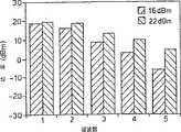
图4示出电吸收(EA)及Mach-Zehnder(MZ)调制器生成的前5个谐波的最大电功率级,(a)示出用电驱动功率+16dBm的理论预测性能,(b)示出用+16dBm电驱动功率的实验观察性能,(c)示出用电驱动功率+22dBm的理论预测性能,(d)示出用电驱动功率+22dBm的实验观察性能;Figure 4 shows the maximum electric power levels of the first 5 harmonics generated by electro-absorption (EA) and Mach-Zehnder (MZ) modulators, (a) shows the theoretically predicted performance with electric drive power +16dBm, (b) shows Show the experimental observation performance with +16dBm electric driving power, (c) show the theoretical prediction performance with electric driving power +22dBm, (d) show the experimental observation performance with electric driving power +22dBm;
图5示出对于电驱动功率+22dBm的带偏压的电谐波功率级的变化(a)对于EA调制器,及(b)对于MZ调制器;以及Figure 5 shows the electrical harmonic power level variation with bias for electrical drive power +22dBm (a) for the EA modulator, and (b) for the MZ modulator; and
图6为展示当与EDFA结合使用时EA调制器所生成的前五个谐波的最大实验观察电功率级的曲线。Figure 6 is a graph showing the maximum experimentally observed electrical power levels for the first five harmonics generated by the EA modulator when used in conjunction with an EDFA.
具体实施方式Detailed ways
图1示出按照本发明的射频调制的光辐射源,包括一个半导体电吸收调制器1及一个射频电辐射源2。半导体电吸收调制器1具有一个光输入端3、一个光输出端4及一个电输入端5。在一个优选的实施例中,如图1所表示的本发明还示出一个电吸收调制器1,该电吸收调制器1包括一个与分布式反馈激光器6集成在一起的光输入端3;该实施例还包括耦合在电吸收调制器1的光输出端4上的光纤7、一个高速光电二极管18及一个RF光谱分析仪19。FIG. 1 shows a radio frequency modulated optical radiation source according to the invention, comprising a
图2更详细地示出电吸收调制器1。电吸收调制器1是用半导体生长领域中的熟练技术人员所知的标准MOVPE技术生长的。电吸收调制器包括一个与光波导结合的反向偏置的PIN结。在一块nInP衬底层9上生长一个nInP缓冲层15。缓冲层15为3μm原并掺杂有1×1018cm-3的硫。在缓冲层15上方生长一个电吸收层14,而在这上面则是一个0.4μm厚的锌5×1017cm-3掺杂的InP层13。这三层13、14与15构成PIN结及光波导两者。为了达到图2中所示的脊状结构,采用了标准光刻法、蚀刻及附生技术。PIN结是嵌入掺铁的1017cm-3(半绝缘的)电流块形结构中的,以便保证作用在电吸收调制器1上的调制电压有效直接地穿过电吸收层14。nInp衬底9用一层TiAu金属化以提供一个接触层8,而该器件的顶部则用一个ASG介电层11钝化。经由P++三元接触层16及一个TiAu接合垫片17接触该器件的顶点。Figure 2 shows the
电吸收层14包括94AInGaAsP阱(λ=1.55μm)与55AInGaAsP隔析(λ=1.1μm)的17周期多量子阱结构。将这一多量子阱结构设计成使得可利用量子约束的Stark效应以技术人员已知方式给出锐吸收特征。为了得出吸收中随作用在电吸收调制器1上的电压的巨大变化,应将多量化阱结构设计成使得在电吸收调制器1上作用一个电场将MQW结构的激子峰值移过电吸收调制器1的工作波长。这里公开的MQW结构已设计成在电吸收调制器的1555nm的输入波长上工作效率最高。在电吸收层14下方为完成PIN结的一个n掺杂的Inp层15。The electro-absorption layer 14 includes a 17-period multi-quantum well structure of 94AlnGaAsP wells (λ=1.55 μm) and 55AlInGaAsP wells (λ=1.1 μm). This multiple quantum well structure is designed in such a way that the quantum-confined Stark effect can be used to give sharp absorption features in a manner known to the skilled person. In order to obtain a large change in absorption with the voltage applied to the
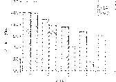
选择电吸收调制器1在光波导的方向上为325μm长。随着电吸收调制器的长度的增加,其电容也增加,其工作速度则降低。然而对于高调制深度,即开闭状态之间的良好对比度,要求通过该器件的高吸收。吸收随器件长度及约束因子增加,然而对于一个给定的作用电压约束因子的增加减小穿过电吸收层的电场。已发现150与350μm之间的电吸收调制器代表这些矛盾的要求之间的良好折衷。电吸收调制器片在端面3与4上涂有抗反射涂层,并封装在一个高速的带有光纤引出端的模件中。测量出器件在1MHz上的电容为0.47pF,并且利用一个15Ω、10nF阻抗匹配电路,封装的电吸收调制器的小信号3dB电带宽为10.7GHz。封装的器件在1555nm的输入波长上具有接通状态光纤到光纤的介入损耗10.8dB。电吸收调制器的测量吸收特征示出在图3中。从图3中可见该器件具有尖锐的吸收特征。The
为了表明电吸收调制器能协调地发生射频调制的光信号的效率,在理论与实验两方面将电吸收调制器与Mach-Zehnder调制器进行比较。用于这一比较的Mach-Zehnder调制器为一从GEC高级光学产品公司(West Hanningfield Road,Great Baddow,Chelmsford,Essex)购得的市场上出售的Ti:LiNbO3MZ调制器(型号Y-35-8931-01)。该Mach-Zehnder调制器具有8GHz的带宽,9.5dB的最小光介入损耗,并在DC调制及在2.5GHZ上的调制下分别具有7.7V及14.9V的Vπ值(将调制器从最大驱动到最小传输所需的作用电压)。这两个值明显地不同,因为当在RF频率上驱动MZ调制器时,采用了一个阻抗变换器将特征阻抗为22Ω的行波电极连接到50Ω输入端上。为了这两个调制器的实验比较使用了图1的配置。将电振荡器2的驱动频率设定为2.5GHz,使得比较结果不受调制器的有限电频率响应的影响。将激光器6对调制器的光输入功率设定为1mW,并用高速光电二极管18(具有18GHz的带宽)及RF频谱分析仪19测定各调制器发生的谐波。在作用在各调制器的DC偏压的范围上测量前五个谐波的功率。对于两种电吸收调制器,为2.5GHz的正弦电波形的作用功率的两个值(+16及+22dBm)取跨接50Ω负载测定的测量值。In order to demonstrate the efficiency with which electroabsorption modulators can coordinately generate radio frequency modulated optical signals, electroabsorption modulators are compared with Mach-Zehnder modulators both theoretically and experimentally. The Mach-Zehnder modulator used for this comparison was a commercially available Ti:LiNbO3 MZ modulator (model Y-35 -8931-01). The Mach-Zehnder modulator has a bandwidth of 8GHz, a minimum optical insertion loss of 9.5dB, and Vπ values of 7.7V and 14.9V for DC modulation and modulation at 2.5GHZ respectively (driving the modulator from maximum to minimum transmit the required active voltage). These two values are significantly different because when driving the MZ modulator at RF frequencies, an impedance transformer is used to connect the traveling-wave electrode with a characteristic impedance of 22Ω to the 50Ω input. For the experimental comparison of these two modulators the configuration of Fig. 1 was used. The driving frequency of the
采用电吸收调制器的谐波发生是通过将一个样条曲线拟合到图3中所示的吸收特征上及计算从作用一个正弦驱动电压所得出的透射光强的傅里叶级数幅值而建立模型的。将结果对1mW的光输入功率正规化,并为转换到RF输出功率假定了理想的光电二极管特征。在计算中使用了实际的调制器介入损耗(10.8dB)。Harmonic generation using an electroabsorption modulator is achieved by fitting a spline curve to the absorption feature shown in Figure 3 and calculating the magnitude of the Fourier series of the transmitted light intensity resulting from the application of a sinusoidal drive voltage And build the model. The results were normalized to an optical input power of 1 mW, and ideal photodiode characteristics were assumed for conversion to RF output power. The actual modulator insertion loss (10.8dB) was used in the calculation.
Mach Zehnder调制器以与电吸收调制器相同的方法建模。作为从系统阻抗(50Ω)到调制器传输线阻抗(22Ω)的内阻抗变换的结果,Vπ的实际值与给定的数字不同。对于所采用的特定调制器,Vπ的实际值计算为15V。Mach Zehnder modulators are modeled in the same way as electroabsorption modulators. The actual value of Vπ differs from the given figure as a result of the internal impedance transformation from the system impedance (50Ω) to the modulator transmission line impedance (22Ω). The actual value of Vπ is calculated to be 15V for the particular modulator employed.
对于两种类型的调制器及两种作用信号电平的各谐波的最大理论预测的及实验达到的RF功率级示出在图4中。画出的值为用一个100%量子效率及无穷大带宽的理想光电二极管所探测到的,从而图4中的各谐波的相对能级与实际光电二极管在该频率上的响应度无关。如能见到的,预测的与实验的结果符合得很好。在两种驱动能级(16与22dBm)上,在发生较高次谐波方面EA调制器比MZ调制器更有效。采用与用于精确地建立图4中所示的调制器性能模型相同的建模方法,计算出为了与在驱动功率+16及+22dBm上采用EA调制器同样有效地生成五次谐波,MZ调制器在驱动频率上必须分别具有低到2.9与4.4V的Vπ值。The maximum theoretically predicted and experimentally achieved RF power levels for each harmonic are shown in FIG. 4 for two types of modulators and two active signal levels. The values plotted are as detected by an ideal photodiode with 100% quantum efficiency and infinite bandwidth, so that the relative energy levels of the harmonics in Figure 4 are independent of the responsivity of the actual photodiode at that frequency. As can be seen, the predicted and experimental results are in good agreement. At both drive levels (16 and 22dBm), the EA modulator is more efficient than the MZ modulator in generating higher harmonics. Using the same modeling approach used to accurately model the modulator performance shown in Figure 4, it was calculated that in order to generate the fifth harmonic as efficiently as using the EA modulator at drive powers of +16 and +22dBm, MZ The modulators must have Vπ values as low as 2.9 and 4.4V, respectively, at the drive frequency.
为了在希望的频率(18,30及60GHz)上为光纤上的无线电应用生成载波,会要求在比EA与MZ性能比较时所用的2.5GHz更高的频率上驱动调制器。EA调制器具有10GHz以上的带宽,因此在电调制频率高于2.5GHz时,预期在这些较高频率上也能高效地生成光载波。没有已知的MZ调制器在足够高的调制频率上具有充分低的Vπ,值足以在使用相同的驱动功率生成五次谐波上与EA调制效率匹敌。To generate carriers at the desired frequencies (18, 30 and 60 GHz) for radio-over-fiber applications would require driving the modulator at a higher frequency than the 2.5 GHz used in the EA vs. MZ performance comparison. EA modulators have bandwidths above 10 GHz, so at electrical modulation frequencies above 2.5 GHz, it is expected that optical carriers can be efficiently generated at these higher frequencies as well. No known MZ modulator has a sufficiently low V[pi] at a high enough modulation frequency to match the efficiency of EA modulation in generating the fifth harmonic with the same driving power.
电吸收调制器与Mach-Zehnder调制器两者的性能都随作用在调制器上的DC偏压明显地变化。这对于电吸收调制器能清楚地从图5a中看出,而对于Mach-Zehnder调制器则从图5b中看出,它们示出对于+22dBm的对抗偏压的电驱动功率,对于相同的输入光功率级及理想的光电二极管的前五个谐波的测定电功率级。The performance of both electroabsorption modulators and Mach-Zehnder modulators varies significantly with the DC bias applied to the modulator. This is clearly seen in Figure 5a for the electroabsorption modulator and Figure 5b for the Mach-Zehnder modulator, which show that for the same input Determination of the optical power level and the first five harmonics of an ideal photodiode's electrical power level.
除了更高效的谐波发生,利用电吸收调制器而不是Mach-Zehnder调制器的又一优点能从图3中推论出。从图3中能看出电吸收调制器的DC与谐波功率级在较高的反向偏置下收敛,而对于Mach-Zehnder调制器的那些则并不。这一收敛是调制深度随反向偏置的增加而增加的结果。从而在适当的偏压上,电吸收调制器具有比Mach-Zehnder更好的调制深度。这不仅对防止光电二极管的饱和重要,也对采用任何光放大器重要。对于给定的光放大器,如果输入光信号具有较高的调制深度并从而具有较低的DC分量,便能在光放大器饱和之前得到更多的有用光增益。Besides more efficient harmonic generation, another advantage of using electro-absorption modulators instead of Mach-Zehnder modulators can be deduced from FIG. 3 . From Fig. 3 it can be seen that the DC and harmonic power levels of the electro-absorption modulator converge at higher reverse bias, while those of the Mach-Zehnder modulator do not. This convergence is a result of the increase in modulation depth with increasing reverse bias. Therefore, at an appropriate bias voltage, the electroabsorption modulator has a better modulation depth than the Mach-Zehnder. This is important not only to prevent saturation of the photodiode, but also to use any optical amplifier. For a given optical amplifier, if the input optical signal has a higher modulation depth and thus a lower DC component, more useful optical gain can be obtained before the optical amplifier saturates.
这一效应是通过利用在输入功率-20dBm以上时输出功率饱和为+15dBm的掺铒光纤放大器来放大从电吸收调制器发出的光信号而实验示出的。EDFA后面随有设定在14dB上的一个光衰减器,以免光电二极管饱和。对作用在EA调制器上的功率+16与+22dBm的2.5GHz信号,进行了电频谱的谐波功率级测定。校正测定的谐波值使之给出在没有光衰减器时从理想的光电二极管生成的电功率级,其结果示出在图6中。随谐波数增加的功率降低小于在不使用EDFA时在相同的驱动功率上观察到的(图4)。从而在传输之前使用一个光放大器来升高信号时,EA调制器能有利地用作光纤上的无线电系统中的谐波发生器。This effect was shown experimentally by amplifying an optical signal from an electro-absorption modulator with an erbium-doped fiber amplifier with an output power saturation of +15 dBm above an input power of -20 dBm. The EDFA is followed by an optical attenuator set at 14dB to avoid saturation of the photodiodes. For 2.5GHz signals with power +16 and +22dBm acting on the EA modulator, the harmonic power level measurement of the electric spectrum was carried out. The measured harmonic values are corrected to give the electrical power levels generated from an ideal photodiode without an optical attenuator, the results of which are shown in FIG. 6 . The power reduction with increasing harmonic number is smaller than that observed at the same drive power without the EDFA (Fig. 4). The EA modulator can thus advantageously be used as a harmonic generator in radio-over-fibre systems when an optical amplifier is used to boost the signal prior to transmission.
虽然在这里利用多量子阱电吸收调制器来描述本发明的特定实施例,技术人员会理解在本发明中也能利用大的半导体电吸收层。在这一情况中可利用Franz-Keldsh效应来增强随作用电压的电吸收调制器吸收中的改变。再者,虽然所描述的电吸收调制器采用反向P-n结结构,技术人员将会理解诸如n-i-n结构或肖特基(Schottky)结构等其它半导体结构也能应用。Although specific embodiments of the invention are described herein utilizing multiple quantum well electroabsorption modulators, skilled artisans will appreciate that large semiconductor electroabsorption layers can also be utilized in the present invention. In this case the Franz-Keldsh effect can be exploited to enhance the change in electro-absorption modulator absorption with applied voltage. Furthermore, although the described electro-absorption modulator adopts an inverted p-n junction structure, the skilled person will understand that other semiconductor structures such as n-i-n structure or Schottky structure can also be used.
Claims (15)
Applications Claiming Priority (4)
| Application Number | Priority Date | Filing Date | Title |
|---|---|---|---|
| WOPCT/GB94/00675 | 1994-03-30 | ||
| PCT/GB1994/000675WO1994023507A1 (en) | 1993-03-31 | 1994-03-30 | Generation of optical signals with rf components |
| EP94305661.4 | 1994-07-29 | ||
| EP94305661 | 1994-07-29 |
Publications (2)
| Publication Number | Publication Date |
|---|---|
| CN1152980A CN1152980A (en) | 1997-06-25 |
| CN1092879Ctrue CN1092879C (en) | 2002-10-16 |
Family
ID=8217794
Family Applications (1)
| Application Number | Title | Priority Date | Filing Date |
|---|---|---|---|
| CN95192396AExpired - Fee RelatedCN1092879C (en) | 1994-03-30 | 1995-03-17 | Generation of radio frequency modulated optical radiation |
Country Status (8)
| Country | Link |
|---|---|
| US (1) | US5917636A (en) |
| EP (1) | EP0772924B1 (en) |
| JP (1) | JP3579057B2 (en) |
| KR (1) | KR100322813B1 (en) |
| CN (1) | CN1092879C (en) |
| CA (1) | CA2185132C (en) |
| DE (1) | DE69525159T2 (en) |
| WO (1) | WO1995027346A1 (en) |
Families Citing this family (62)
| Publication number | Priority date | Publication date | Assignee | Title |
|---|---|---|---|---|
| KR100555996B1 (en)* | 1996-07-19 | 2006-07-06 | 넥스트지 네트웍스 인코퍼레이티드 | Telecommunication system that receives and modulates optical signals simultaneously |
| JP3839574B2 (en)* | 1998-01-12 | 2006-11-01 | 株式会社沖コムテック | Bias voltage control circuit for avalanche photodiode and adjustment method thereof |
| US6359716B1 (en)* | 1999-02-24 | 2002-03-19 | Massachusetts Institute Of Technology | All-optical analog FM optical receiver |
| DE10201126A1 (en)* | 2002-01-09 | 2003-07-24 | Infineon Technologies Ag | Optoelectronic component has monolithic light source and photodetector monitoring light output for regulation of optoelectronic component |
| EP1361683A1 (en)* | 2002-02-08 | 2003-11-12 | Motorola, Inc. | Optical to radio frequency detector |
| DE10303676A1 (en)* | 2003-01-24 | 2004-09-02 | Infineon Technologies Ag | Electrooptical component for generating millimeter and sub-millimeter waves has millimeter and sub-millimeter wave antenna and optical receiver in form of electro-absorption modulator |
| US7751722B2 (en)* | 2003-02-07 | 2010-07-06 | Panasonic Corporation | Optical transmission system |
| US7280568B2 (en)* | 2003-08-29 | 2007-10-09 | New Focus, Inc. | Laser coherence control using homogeneous linewidth broadening |
| WO2007145144A1 (en)* | 2006-06-14 | 2007-12-21 | Anritsu Corporation | Optical modulator |
| US7787823B2 (en) | 2006-09-15 | 2010-08-31 | Corning Cable Systems Llc | Radio-over-fiber (RoF) optical fiber cable system with transponder diversity and RoF wireless picocellular system using same |
| US7848654B2 (en) | 2006-09-28 | 2010-12-07 | Corning Cable Systems Llc | Radio-over-fiber (RoF) wireless picocellular system with combined picocells |
| US8873585B2 (en) | 2006-12-19 | 2014-10-28 | Corning Optical Communications Wireless Ltd | Distributed antenna system for MIMO technologies |
| US8111998B2 (en) | 2007-02-06 | 2012-02-07 | Corning Cable Systems Llc | Transponder systems and methods for radio-over-fiber (RoF) wireless picocellular systems |
| US20100054746A1 (en) | 2007-07-24 | 2010-03-04 | Eric Raymond Logan | Multi-port accumulator for radio-over-fiber (RoF) wireless picocellular systems |
| US8175459B2 (en)* | 2007-10-12 | 2012-05-08 | Corning Cable Systems Llc | Hybrid wireless/wired RoF transponder and hybrid RoF communication system using same |
| US8644844B2 (en) | 2007-12-20 | 2014-02-04 | Corning Mobileaccess Ltd. | Extending outdoor location based services and applications into enclosed areas |
| WO2009114738A2 (en) | 2008-03-12 | 2009-09-17 | Hypres, Inc. | Digital radio-frequency tranceiver system and method |
| US8693875B2 (en)* | 2008-11-20 | 2014-04-08 | Applied Communications Sciences | Method and apparatus for optimized analog RF optical links |
| CN102369678B (en) | 2009-02-03 | 2015-08-19 | 康宁光缆系统有限责任公司 | Optical fiber based distributed antenna systems, assemblies and related methods for calibrating optical fiber based distributed antenna systems, assemblies |
| CN102396171B (en) | 2009-02-03 | 2015-09-30 | 康宁光缆系统有限责任公司 | Based on the distributing antenna system of optical fiber, assembly and the correlation technique for monitoring and configure distributing antenna system based on optical fiber, assembly |
| US9673904B2 (en) | 2009-02-03 | 2017-06-06 | Corning Optical Communications LLC | Optical fiber-based distributed antenna systems, components, and related methods for calibration thereof |
| US8548330B2 (en) | 2009-07-31 | 2013-10-01 | Corning Cable Systems Llc | Sectorization in distributed antenna systems, and related components and methods |
| US8280259B2 (en) | 2009-11-13 | 2012-10-02 | Corning Cable Systems Llc | Radio-over-fiber (RoF) system for protocol-independent wired and/or wireless communication |
| US8275265B2 (en) | 2010-02-15 | 2012-09-25 | Corning Cable Systems Llc | Dynamic cell bonding (DCB) for radio-over-fiber (RoF)-based networks and communication systems and related methods |
| US9525488B2 (en) | 2010-05-02 | 2016-12-20 | Corning Optical Communications LLC | Digital data services and/or power distribution in optical fiber-based distributed communications systems providing digital data and radio frequency (RF) communications services, and related components and methods |
| US20110268446A1 (en) | 2010-05-02 | 2011-11-03 | Cune William P | Providing digital data services in optical fiber-based distributed radio frequency (rf) communications systems, and related components and methods |
| WO2012024247A1 (en) | 2010-08-16 | 2012-02-23 | Corning Cable Systems Llc | Remote antenna clusters and related systems, components, and methods supporting digital data signal propagation between remote antenna units |
| US9252874B2 (en) | 2010-10-13 | 2016-02-02 | Ccs Technology, Inc | Power management for remote antenna units in distributed antenna systems |
| EP2678972B1 (en) | 2011-02-21 | 2018-09-05 | Corning Optical Communications LLC | Providing digital data services as electrical signals and radio-frequency (rf) communications over optical fiber in distributed communications systems, and related components and methods |
| WO2012148938A1 (en) | 2011-04-29 | 2012-11-01 | Corning Cable Systems Llc | Determining propagation delay of communications in distributed antenna systems, and related components, systems and methods |
| WO2012148940A1 (en) | 2011-04-29 | 2012-11-01 | Corning Cable Systems Llc | Systems, methods, and devices for increasing radio frequency (rf) power in distributed antenna systems |
| EP2832012A1 (en) | 2012-03-30 | 2015-02-04 | Corning Optical Communications LLC | Reducing location-dependent interference in distributed antenna systems operating in multiple-input, multiple-output (mimo) configuration, and related components, systems, and methods |
| WO2013162988A1 (en) | 2012-04-25 | 2013-10-31 | Corning Cable Systems Llc | Distributed antenna system architectures |
| WO2014024192A1 (en) | 2012-08-07 | 2014-02-13 | Corning Mobile Access Ltd. | Distribution of time-division multiplexed (tdm) management services in a distributed antenna system, and related components, systems, and methods |
| US9455784B2 (en) | 2012-10-31 | 2016-09-27 | Corning Optical Communications Wireless Ltd | Deployable wireless infrastructures and methods of deploying wireless infrastructures |
| CN105308876B (en) | 2012-11-29 | 2018-06-22 | 康宁光电通信有限责任公司 | Remote unit antennas in distributing antenna system combines |
| US9647758B2 (en) | 2012-11-30 | 2017-05-09 | Corning Optical Communications Wireless Ltd | Cabling connectivity monitoring and verification |
| CN105452951B (en) | 2013-06-12 | 2018-10-19 | 康宁光电通信无线公司 | Voltage type optical directional coupler |
| WO2014199380A1 (en) | 2013-06-12 | 2014-12-18 | Corning Optical Communications Wireless, Ltd. | Time-division duplexing (tdd) in distributed communications systems, including distributed antenna systems (dass) |
| US9247543B2 (en) | 2013-07-23 | 2016-01-26 | Corning Optical Communications Wireless Ltd | Monitoring non-supported wireless spectrum within coverage areas of distributed antenna systems (DASs) |
| US9599504B2 (en)* | 2013-07-30 | 2017-03-21 | Raytheon Company | Fiber optic vibration detection |
| US9661781B2 (en) | 2013-07-31 | 2017-05-23 | Corning Optical Communications Wireless Ltd | Remote units for distributed communication systems and related installation methods and apparatuses |
| US9385810B2 (en) | 2013-09-30 | 2016-07-05 | Corning Optical Communications Wireless Ltd | Connection mapping in distributed communication systems |
| US9178635B2 (en) | 2014-01-03 | 2015-11-03 | Corning Optical Communications Wireless Ltd | Separation of communication signal sub-bands in distributed antenna systems (DASs) to reduce interference |
| US9775123B2 (en) | 2014-03-28 | 2017-09-26 | Corning Optical Communications Wireless Ltd. | Individualized gain control of uplink paths in remote units in a distributed antenna system (DAS) based on individual remote unit contribution to combined uplink power |
| US9357551B2 (en) | 2014-05-30 | 2016-05-31 | Corning Optical Communications Wireless Ltd | Systems and methods for simultaneous sampling of serial digital data streams from multiple analog-to-digital converters (ADCS), including in distributed antenna systems |
| US9525472B2 (en) | 2014-07-30 | 2016-12-20 | Corning Incorporated | Reducing location-dependent destructive interference in distributed antenna systems (DASS) operating in multiple-input, multiple-output (MIMO) configuration, and related components, systems, and methods |
| US9730228B2 (en) | 2014-08-29 | 2017-08-08 | Corning Optical Communications Wireless Ltd | Individualized gain control of remote uplink band paths in a remote unit in a distributed antenna system (DAS), based on combined uplink power level in the remote unit |
| US9602210B2 (en) | 2014-09-24 | 2017-03-21 | Corning Optical Communications Wireless Ltd | Flexible head-end chassis supporting automatic identification and interconnection of radio interface modules and optical interface modules in an optical fiber-based distributed antenna system (DAS) |
| US10659163B2 (en) | 2014-09-25 | 2020-05-19 | Corning Optical Communications LLC | Supporting analog remote antenna units (RAUs) in digital distributed antenna systems (DASs) using analog RAU digital adaptors |
| US9420542B2 (en) | 2014-09-25 | 2016-08-16 | Corning Optical Communications Wireless Ltd | System-wide uplink band gain control in a distributed antenna system (DAS), based on per band gain control of remote uplink paths in remote units |
| WO2016071902A1 (en) | 2014-11-03 | 2016-05-12 | Corning Optical Communications Wireless Ltd. | Multi-band monopole planar antennas configured to facilitate improved radio frequency (rf) isolation in multiple-input multiple-output (mimo) antenna arrangement |
| WO2016075696A1 (en) | 2014-11-13 | 2016-05-19 | Corning Optical Communications Wireless Ltd. | Analog distributed antenna systems (dass) supporting distribution of digital communications signals interfaced from a digital signal source and analog radio frequency (rf) communications signals |
| US9729267B2 (en) | 2014-12-11 | 2017-08-08 | Corning Optical Communications Wireless Ltd | Multiplexing two separate optical links with the same wavelength using asymmetric combining and splitting |
| WO2016098109A1 (en) | 2014-12-18 | 2016-06-23 | Corning Optical Communications Wireless Ltd. | Digital interface modules (dims) for flexibly distributing digital and/or analog communications signals in wide-area analog distributed antenna systems (dass) |
| WO2016098111A1 (en) | 2014-12-18 | 2016-06-23 | Corning Optical Communications Wireless Ltd. | Digital- analog interface modules (da!ms) for flexibly.distributing digital and/or analog communications signals in wide-area analog distributed antenna systems (dass) |
| US20160249365A1 (en) | 2015-02-19 | 2016-08-25 | Corning Optical Communications Wireless Ltd. | Offsetting unwanted downlink interference signals in an uplink path in a distributed antenna system (das) |
| US9681313B2 (en) | 2015-04-15 | 2017-06-13 | Corning Optical Communications Wireless Ltd | Optimizing remote antenna unit performance using an alternative data channel |
| US9948349B2 (en) | 2015-07-17 | 2018-04-17 | Corning Optical Communications Wireless Ltd | IOT automation and data collection system |
| US10560214B2 (en) | 2015-09-28 | 2020-02-11 | Corning Optical Communications LLC | Downlink and uplink communication path switching in a time-division duplex (TDD) distributed antenna system (DAS) |
| EP3417553A1 (en)* | 2016-02-19 | 2018-12-26 | BAE Systems PLC | Optical sensing and communications system |
| US10236924B2 (en) | 2016-03-31 | 2019-03-19 | Corning Optical Communications Wireless Ltd | Reducing out-of-channel noise in a wireless distribution system (WDS) |
Family Cites Families (2)
| Publication number | Priority date | Publication date | Assignee | Title |
|---|---|---|---|---|
| JPH022727A (en)* | 1988-06-17 | 1990-01-08 | Shiyoudenriyoku Kosoku Tsushin Kenkyusho:Kk | Radio wave transmission/reception system via optical fiber |
| JP2819080B2 (en)* | 1993-03-25 | 1998-10-30 | 国際電信電話株式会社 | Optical pulse generator |
- 1995
- 1995-03-17CNCN95192396Apatent/CN1092879C/ennot_activeExpired - Fee Related
- 1995-03-17KRKR1019960705240Apatent/KR100322813B1/ennot_activeExpired - Fee Related
- 1995-03-17JPJP52548295Apatent/JP3579057B2/ennot_activeExpired - Fee Related
- 1995-03-17EPEP95911421Apatent/EP0772924B1/ennot_activeExpired - Lifetime
- 1995-03-17CACA002185132Apatent/CA2185132C/ennot_activeExpired - Fee Related
- 1995-03-17WOPCT/GB1995/000589patent/WO1995027346A1/enactiveIP Right Grant
- 1995-03-17USUS08/716,187patent/US5917636A/ennot_activeExpired - Lifetime
- 1995-03-17DEDE69525159Tpatent/DE69525159T2/ennot_activeExpired - Lifetime
Non-Patent Citations (2)
| Title |
|---|
| IEICE TRANSACTIONS ON COMMUNICATIONS VOL E 76B NO 9 1993.9.1 OGAWA MICTOWAVE AND MILLIMETREWAVE FIBRE OPTIC TECHNOLOGIES FOR SUBCARRIER* |
| OPTICAL TECHNOLOGY FOR MICROWAVE APPLICATIONS VI 1992.4.1 YU ET AL DESIGN AND FABTICATION OF INGAASP/INP WAVEGUIDE MODULATORS FOR MI* |
Also Published As
| Publication number | Publication date |
|---|---|
| CN1152980A (en) | 1997-06-25 |
| JP3579057B2 (en) | 2004-10-20 |
| US5917636A (en) | 1999-06-29 |
| EP0772924B1 (en) | 2002-01-23 |
| DE69525159D1 (en) | 2002-03-14 |
| CA2185132A1 (en) | 1995-10-12 |
| CA2185132C (en) | 2000-09-26 |
| EP0772924A1 (en) | 1997-05-14 |
| DE69525159T2 (en) | 2002-08-22 |
| WO1995027346A1 (en) | 1995-10-12 |
| KR970701954A (en) | 1997-04-12 |
| JPH09511075A (en) | 1997-11-04 |
| KR100322813B1 (en) | 2002-06-26 |
Similar Documents
| Publication | Publication Date | Title |
|---|---|---|
| CN1092879C (en) | Generation of radio frequency modulated optical radiation | |
| US9059801B1 (en) | Optical modulator | |
| CN101222121A (en) | Integrated optoelectronic devices for high-frequency microwave generation using SOA four-wave mixing effect | |
| Westbrook et al. | Simultaneous bi-directional analogue fibre-optic transmission using an electroabsorption modulator | |
| Kaneko et al. | An electroabsorption modulator module for digital and analog applications | |
| CN101566777A (en) | Integrated optoelectronic device based on sideband injection locking and used for generating high-frequency microwaves | |
| Jager et al. | Microwave photonics | |
| EP1335239B1 (en) | Conversion between optical and radio frequency signals | |
| CN113703201B (en) | Optical modulator and control method thereof | |
| Loi et al. | Low-loss 1.3-μm MQW electroabsorption modulators for high-linearity analog optical links | |
| Moodie et al. | Efficient harmonic generation using an electroabsorption modulator | |
| US7877015B2 (en) | Optical to radio frequency detector | |
| Johansson et al. | High optical power electroabsorption waveguide modulator | |
| KR100715865B1 (en) | All-optical Frequency Upconversion Method Using Semiconductor Optical Amplifier Mach-Zehnder Interferometer | |
| Devaux et al. | Lossless InAsP-InGaP modulator at 1.3 μm for optical conversion of radio signals up to 40 GHz | |
| Mohammed et al. | Recent applications of the electrooptic modulators in radio-over-fiber (ROF) | |
| Westergren et al. | Compact and efficient modulators forá100áGb/s ETDM forátelecom and interconnect applications | |
| Nadeem et al. | Recent Advancement on Photonic Feeding of Antennas for Microwave Beam Steering | |
| Chung et al. | Analog characteristics of electroabsorption modulator for RF/optic conversion; RF gain and IMD3 | |
| FUKUSHIMA et al. | Optically-fed radio access point module for a fibre-radio downlink system | |
| Avo et al. | 60 GHz radio-over-fiber transmission impairments for broadband wireless signals | |
| CN111835424A (en) | Millimeter wave generating system for generating six-time frequency vector and using method thereof | |
| Choa | High-efficiency directly modulated laser links | |
| Chung et al. | RF gain and IMD Characteristics of Electroabsorption Modulator for Analog Applications | |
| Han et al. | Characterization of loss-coupled 1550ánm DFB lasers for microwave optical links |
Legal Events
| Date | Code | Title | Description |
|---|---|---|---|
| C06 | Publication | ||
| PB01 | Publication | ||
| C10 | Entry into substantive examination | ||
| SE01 | Entry into force of request for substantive examination | ||
| C14 | Grant of patent or utility model | ||
| GR01 | Patent grant | ||
| C17 | Cessation of patent right | ||
| CF01 | Termination of patent right due to non-payment of annual fee | Granted publication date:20021016 Termination date:20110317 |