CN109256170B - Memory cell and memory array - Google Patents
Memory cell and memory arrayDownload PDFInfo
- Publication number
- CN109256170B CN109256170BCN201710564873.9ACN201710564873ACN109256170BCN 109256170 BCN109256170 BCN 109256170BCN 201710564873 ACN201710564873 ACN 201710564873ACN 109256170 BCN109256170 BCN 109256170B
- Authority
- CN
- China
- Prior art keywords
- voltage
- memory cell
- coupled
- read
- write
- Prior art date
- Legal status (The legal status is an assumption and is not a legal conclusion. Google has not performed a legal analysis and makes no representation as to the accuracy of the status listed.)
- Active
Links
Images


Classifications
- G—PHYSICS
- G11—INFORMATION STORAGE
- G11C—STATIC STORES
- G11C7/00—Arrangements for writing information into, or reading information out from, a digital store
- G11C7/12—Bit line control circuits, e.g. drivers, boosters, pull-up circuits, pull-down circuits, precharging circuits, equalising circuits, for bit lines
- G—PHYSICS
- G11—INFORMATION STORAGE
- G11C—STATIC STORES
- G11C17/00—Read-only memories programmable only once; Semi-permanent stores, e.g. manually-replaceable information cards
- G11C17/14—Read-only memories programmable only once; Semi-permanent stores, e.g. manually-replaceable information cards in which contents are determined by selectively establishing, breaking or modifying connecting links by permanently altering the state of coupling elements, e.g. PROM
- G11C17/18—Auxiliary circuits, e.g. for writing into memory
- G—PHYSICS
- G11—INFORMATION STORAGE
- G11C—STATIC STORES
- G11C11/00—Digital stores characterised by the use of particular electric or magnetic storage elements; Storage elements therefor
- G11C11/56—Digital stores characterised by the use of particular electric or magnetic storage elements; Storage elements therefor using storage elements with more than two stable states represented by steps, e.g. of voltage, current, phase, frequency
- G11C11/5692—Digital stores characterised by the use of particular electric or magnetic storage elements; Storage elements therefor using storage elements with more than two stable states represented by steps, e.g. of voltage, current, phase, frequency read-only digital stores using storage elements with more than two stable states
- G—PHYSICS
- G11—INFORMATION STORAGE
- G11C—STATIC STORES
- G11C17/00—Read-only memories programmable only once; Semi-permanent stores, e.g. manually-replaceable information cards
- G11C17/14—Read-only memories programmable only once; Semi-permanent stores, e.g. manually-replaceable information cards in which contents are determined by selectively establishing, breaking or modifying connecting links by permanently altering the state of coupling elements, e.g. PROM
- G11C17/16—Read-only memories programmable only once; Semi-permanent stores, e.g. manually-replaceable information cards in which contents are determined by selectively establishing, breaking or modifying connecting links by permanently altering the state of coupling elements, e.g. PROM using electrically-fusible links
- G—PHYSICS
- G11—INFORMATION STORAGE
- G11C—STATIC STORES
- G11C5/00—Details of stores covered by group G11C11/00
- G11C5/06—Arrangements for interconnecting storage elements electrically, e.g. by wiring
- G—PHYSICS
- G11—INFORMATION STORAGE
- G11C—STATIC STORES
- G11C8/00—Arrangements for selecting an address in a digital store
- G11C8/14—Word line organisation; Word line lay-out
- H—ELECTRICITY
- H03—ELECTRONIC CIRCUITRY
- H03K—PULSE TECHNIQUE
- H03K19/00—Logic circuits, i.e. having at least two inputs acting on one output; Inverting circuits
- H03K19/0175—Coupling arrangements; Interface arrangements
- H03K19/0185—Coupling arrangements; Interface arrangements using field effect transistors only
- H03K19/018507—Interface arrangements
- G—PHYSICS
- G11—INFORMATION STORAGE
- G11C—STATIC STORES
- G11C5/00—Details of stores covered by group G11C11/00
- G11C5/06—Arrangements for interconnecting storage elements electrically, e.g. by wiring
- G11C5/063—Voltage and signal distribution in integrated semi-conductor memory access lines, e.g. word-line, bit-line, cross-over resistance, propagation delay
Landscapes
- Engineering & Computer Science (AREA)
- Computer Hardware Design (AREA)
- Physics & Mathematics (AREA)
- Computing Systems (AREA)
- General Engineering & Computer Science (AREA)
- Mathematical Physics (AREA)
- Microelectronics & Electronic Packaging (AREA)
- Read Only Memory (AREA)
Abstract
Translated fromChinese
Description
Translated fromChinese技术领域technical field
本发明是有关于一种存储单元,特别是有关于一种具有读取选择晶体管及写入选择晶体管的存储单元。The present invention relates to a memory cell, in particular, to a memory cell having a read select transistor and a write select transistor.
背景技术Background technique
非易失性存储器(non-volatile memory,NVM)是一种在没有电力供应至存储区块的情况下,仍然能够维持原本储存之数据的存储器,也因其特性,而被广泛地应用在各种领域。可编程只读存储器(Programmable Read-Only Memory,PROM)是其中一种常见的非易失性存储器。先前技术的可编程只读存储器内部具有行列式的镕丝,并可依照使用上的需求,导通电流将熔丝烧断,以写入所需的数据。熔丝一旦烧断,就无法再恢复,因此可编程只读存储器在第一次被写入后就无法再重复写入其他数据,而只能提供其他电路读取数据。Non-volatile memory (NVM) is a kind of memory that can still maintain the original stored data without power supply to the storage block. It is also widely used in various kinds of fields. Programmable Read-Only Memory (Programmable Read-Only Memory, PROM) is one of the common non-volatile memories. The programmable read-only memory of the prior art has a determinant fuse inside, and according to the requirements of use, the fuse can be blown by conducting current to write the required data. Once the fuse is blown, it cannot be recovered, so the programmable read-only memory cannot write other data repeatedly after being written for the first time, but can only provide other circuits to read the data.
现有技术的可编程只读存储器常利用反熔丝电容来取代熔丝。利用高电压将反熔丝电容击穿来改变其电阻值,即可将所需的数据写入。利用反熔丝电容来实际操作,能够提高芯片探针(Chip Probe,CP)及最终测试(Final Test,FT)的效率,进而提升可编程只读存储器的良率。此外,为了有效控制可编程只读存储器中的每一个存储单元,使得可编程只读存储器能够根据需求对特定的存储单元进行写入操作或读取操作,因此在存储单元的布局以及操作弹性的方面,仍面临挑战。Prior art programmable read only memories often utilize anti-fuse capacitors in place of fuses. Using high voltage to break down the anti-fuse capacitor to change its resistance value, the required data can be written. Using the anti-fuse capacitor for actual operation can improve the efficiency of chip probe (Chip Probe, CP) and final test (Final Test, FT), thereby improving the yield rate of programmable read-only memory. In addition, in order to effectively control each storage unit in the programmable read-only memory, the programmable read-only memory can perform a write operation or a read operation on a specific storage unit according to requirements, so the layout and operation flexibility of the storage unit are flexible. On the other hand, challenges remain.
发明内容SUMMARY OF THE INVENTION
本发明的一实施例提供一种存储单元,存储单元包括读取选择晶体管、写入选择晶体管及反熔丝电容。An embodiment of the present invention provides a memory cell including a read selection transistor, a write selection transistor and an anti-fuse capacitor.
读取选择晶体管具有第一端、第二端及控制端,读取选择晶体管的第一端耦接于位线,而读取选择晶体管的控制端耦接于读取字符线。写入选择晶体管具有第一端、第二端及控制端,写入选择晶体管的第一端耦接于读取选择晶体管的第二端,写入选择晶体管的第二端耦接于高压控制线,而写入选择晶体管的控制端耦接于写入字符线。反熔丝电容具有第一端及第二端,反熔丝电容的第一端耦接于读取选择晶体管的第二端,而反熔丝电容的第二端耦接于低压控制线。The read select transistor has a first end, a second end and a control end, the first end of the read select transistor is coupled to the bit line, and the control end of the read select transistor is coupled to the read word line. The write select transistor has a first end, a second end and a control end, the first end of the write select transistor is coupled to the second end of the read select transistor, and the second end of the write select transistor is coupled to the high voltage control line , and the control terminal of the write select transistor is coupled to the write word line. The anti-fuse capacitor has a first terminal and a second terminal, the first terminal of the anti-fuse capacitor is coupled to the second terminal of the read selection transistor, and the second terminal of the anti-fuse capacitor is coupled to the low-voltage control line.
本发明的另一实施例提供一种存储阵列,存储阵列包括多条位线、多条读取字符线、多条写入字符线、多条高压控制线、多条低压控制线及多行存储单元。Another embodiment of the present invention provides a memory array including a plurality of bit lines, a plurality of read word lines, a plurality of write word lines, a plurality of high voltage control lines, a plurality of low voltage control lines, and a plurality of rows of memory unit.
每一存储单元包括读取选择晶体管、写入选择晶体管及反熔丝电容。读取选择晶体管具有第一端、第二端及控制端,读取选择晶体管的第一端耦接于对应的位线,而读取选择晶体管的控制端耦接于对应的读取字符线。写入选择晶体管具有第一端、第二端及控制端,写入选择晶体管的第一端耦接于读取选择晶体管的第二端,写入选择晶体管的第二端耦接于对应的高压控制线,而写入选择晶体管的控制端耦接于对应的写入字符线。反熔丝电容具有第一端及第二端,反熔丝电容的第一端耦接于读取选择晶体管的第二端,而反熔丝电容的第二端耦接于对应的低压控制线。Each memory cell includes a read select transistor, a write select transistor and an anti-fuse capacitor. The read select transistor has a first end, a second end and a control end, the first end of the read select transistor is coupled to the corresponding bit line, and the control end of the read select transistor is coupled to the corresponding read word line. The write select transistor has a first end, a second end and a control end, the first end of the write select transistor is coupled to the second end of the read select transistor, and the second end of the write select transistor is coupled to the corresponding high voltage control line, and the control terminal of the write select transistor is coupled to the corresponding write word line. The anti-fuse capacitor has a first end and a second end, the first end of the anti-fuse capacitor is coupled to the second end of the read selection transistor, and the second end of the anti-fuse capacitor is coupled to the corresponding low-voltage control line .
附图说明Description of drawings
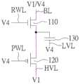
图1为本发明一实施例的存储单元的示意图;FIG. 1 is a schematic diagram of a storage unit according to an embodiment of the present invention;
图2为图1的存储单元在写入操作期间所接收到的信号电压示意图;2 is a schematic diagram of signal voltages received by the memory cell of FIG. 1 during a write operation;
图3为图1的存储单元在读取操作期间所接收到的信号电压示意图;3 is a schematic diagram of signal voltages received by the memory cell of FIG. 1 during a read operation;
图4为本发明一实施例的存储阵列的示意图;FIG. 4 is a schematic diagram of a storage array according to an embodiment of the present invention;
图5为图4的存储阵列中,存储单元的写入操作期间的信号电压示意图;5 is a schematic diagram of signal voltages during a write operation of memory cells in the memory array of FIG. 4;
图6为图4的存储阵列中,存储单元的读取操作期间的信号电压示意图。【主要组件符号说明】FIG. 6 is a schematic diagram of signal voltages during a read operation of memory cells in the memory array of FIG. 4 . 【Description of main component symbols】
10 存储阵列10 Storage arrays
100、100(1,1)至100(M,N) 存储单元100, 100(1,1) to 100(M,N) memory cells
110 读取选择晶体管110 Read select transistor
120 写入选择晶体管120 Write select transistor
130 反熔丝电容130 Antifuse capacitor
BL、BL1至BLM 位线BL, BL1 to BLM bit lines
LVL、LVL1至LVLN 低压控制线LVL, LVL1 to LVLN Low Voltage Control Lines
HVL、HVL1至HVLK 高压控制线HVL, HVL1 to HVLK high voltage control lines
RWL、RWL1至RWLN 读取字符线RWL, RWL1 to RWLN Read character lines
PWL、PWL1至PWLM 写入字符线PWL, PWL1 to PWLM Write word lines
V1 第一电压V1 first voltage
V2 第二电压V2 second voltage
V3 第三电压V3 third voltage
V4 第四电压V4 fourth voltage
V5 第五电压V5 fifth voltage
具体实施方式Detailed ways
图1为本发明一实施例的存储单元100的示意图。存储单元100包括读取选择晶体管110、写入选择晶体管120及反熔丝电容130。FIG. 1 is a schematic diagram of a
读取选择晶体管110具有第一端、第二端及控制端,读取选择晶体管110的第一端耦接于位线BL,而读取选择晶体管110的控制端耦接于读取字符线RWL。写入选择晶体管120具有第一端、第二端及控制端,写入选择晶体管120的第一端耦接于读取选择晶体管110的第二端,写入选择晶体管120的第二端耦接于高压控制线HVL,而写入选择晶体管120的控制端耦接于写入字符线PWL。反熔丝电容130具有第一端及第二端,反熔丝电容130的第一端耦接于读取选择晶体管110的第二端,而反熔丝电容130的第二端耦接于低压控制线LVL。The read
在图1的实施例中,读取选择晶体管110可为N型晶体管,而写入选择晶体管120可为P型晶体管。如此一来,当欲导通写入选择晶体管120以使反熔丝电容130接收到高压控制线HVL的高电压时,即可利用低电压导通写入选择晶体管120,以简化系统的电力设计。In the embodiment of FIG. 1 , the read
此外,反熔丝电容130可利用N型晶体管来实际操作,举例来说,反熔丝电容130的第一端可为N型晶体管的栅极结构,而反熔丝电容130的第二端则可为N型参杂区。In addition, the
图2为存储单元100在写入操作期间所接收到的信号电压示意图。在存储单元100的写入操作期间,位线BL、读取字符线RWL及写入字符线PWL都处在第一电压V1,高压控制线HVL处在第二电压V2,而低压控制线LVL处在第三电压V3。在本发明的部分实施例中,第二电压V2可大于第一电压V1,且第一电压V1可大于第三电压V3。举例来说,第二电压V2可为4V,第一电压V1可为0V,而第三电压V3可为-2V。FIG. 2 is a schematic diagram of signal voltages received by the
在写入操作期间,读取选择晶体管110会被截止,而写入选择晶体管120会被导通。因此反熔丝电容130的第一端会经由写入选择晶体管120接收到高压控制线HVL的第二电压V2,而反熔丝电容130的第二端则会接收低压控制线LVL的第三电压V3。此时第二电压V2与第三电压V3之间的巨大电压差将使得反熔丝电容130被击穿,因此数据能够被写入存储单元100。During a write operation, the read
图3为存储单元100在读取操作期间所接收到的信号电压示意图。在存储单元100的读取操作期间,读取字符线RWL、写入字符线PWL及低压控制线LVL都处在第四电压V4,而高压控制线HVL则处在第一电压V1。在本发明的部分实施例中,第四电压V4可大于第一电压V1,并足以使读取选择晶体管110导通且使写入选择晶体管120截止。此外,第四电压V4可小于第二电压V2。举例来说,第二电压V2可为4V,第一电压V1可为0V,而第四电压V4可为1.2V。FIG. 3 is a schematic diagram of signal voltages received by the
在读取操作期间,读取选择晶体管110可被导通,而写入选择晶体管120会被截止。此时反熔丝电容130的第二端会接收低压控制线LVL的第四电压V4,由于反熔丝电容130被击穿前后的特性不同,因此位线BL的电压也会有所差异。举例来说,在反熔丝电容130被击穿,亦即存储单元100已被写入的状态下,位线BL会经由读取选晶体管110被充电至接近第四电压V4。反之,在反熔丝电容130未被击穿,亦即存储单元100未被写入的状态下,位线BL的电压则会处于第一电压V1。因此通过判断位线BL的电压大小就能够判读存储单元100中储存的数据。During a read operation, the read
图4为本发明一实施例的存储阵列10的示意图。存储阵列10包括M条位线BL1至BLM、N条读取字符线RWL1至RWLN、M条写入字符线PWL1至PLWM、K条高压控制线HVL1至HVLK、N条低压控制线LVL1至LVLN及多个存储单元100(1,1)至100(M,N)。N、M为正偶数,而K可为N的一半。FIG. 4 is a schematic diagram of the
存储单元100(1,1)至100(M,N)可利用图1所示的存储单元100来实际操作,也就是说,每一个存储单元100(1,1)至100(M,N)可包含读取选择晶体管110、写入选择晶体管120及反熔丝电容130,并且会耦接于对应的位线、读取字符线、写入字符线、高压控制线及低压控制线。The memory cells 100(1,1) to 100(M,N) may actually operate using the
在图4中,存储单元100(1,1)至100(M,N)可设置成列,举例来说存储单元100(1,1)至100(M,1)可设置于同一行,而100(1,N)至100(M,N)可设置于同一行。在此情况下,位于同一行的多个存储单元可耦接于相同的读取字符线、相同的低压控制线及相同的高压控制线,并耦接于相异的多条写入字符线及相异的多条位线。In FIG. 4, the memory cells 100(1,1) to 100(M,N) can be arranged in columns, for example, the memory cells 100(1,1) to 100(M,1) can be arranged in the same row, and 100(1,N) to 100(M,N) can be set in the same row. In this case, a plurality of memory cells in the same row can be coupled to the same read word line, the same low-voltage control line and the same high-voltage control line, and to different write word lines and Distinct multiple bit lines.
举例来说,存储单元100(1,1)至100(M,1)会耦接于读取字符线RWL1、低压控制线LVL1及高压控制线HVL1,且存储单元100(1,1)会耦接于写入字符线PWL1及位线BL1,而存储单元100(M,1)则会耦接于写入字符线PWLM及位线BLM。For example, memory cells 100(1,1) to 100(M,1) are coupled to read word line RWL1, low voltage control line LVL1 and high voltage control line HVL1, and memory cell 100(1,1) is coupled to It is connected to the write word line PWL1 and the bit line BL1, and the memory cell 100(M, 1) is coupled to the write word line PWLM and the bit line BLM.
此外,位于同一列的存储单元则会耦接于相同的写入字符线及位线。举例来说,存储单元100(1,1)及100(1,N)设置于同一列,而100(M,1)及100(M,N)设置于同一列。存储单元100(1,1)及100(1,N)可耦接于写入字符线PWL1及位线BL1,而存储单元100(M,1)及100(M,N)则可耦接于写入字符线PWLM及位线BLM。In addition, the memory cells in the same column are coupled to the same write word line and bit line. For example, memory cells 100(1,1) and 100(1,N) are arranged in the same column, and 100(M,1) and 100(M,N) are arranged in the same column. Memory cells 100(1,1) and 100(1,N) may be coupled to write word line PWL1 and bit line BL1, while memory cells 100(M,1) and 100(M,N) may be coupled to Write word line PWLM and bit line BLM.
在图4的实施例中,位于同一列的相邻存储单元还可彼此相耦接,进而减少布局面积并简化绕线。举例来说,存储单元100(1,1)及存储单元位100(1,2)位于相邻两行且位于同一列,且存储单元100(1,1)的写入选择晶体管120的第二端可耦接于存储单元100(1,2)的写入选择晶体管120的第二端。此时,存储单元100(1,1)的写入选择晶体管120会与存储单元100(1,2)的写入选择晶体管120耦接于相同的高压控制线HVL1。In the embodiment of FIG. 4 , adjacent memory cells located in the same column can also be coupled to each other, thereby reducing the layout area and simplifying the routing. For example, memory cell 100(1,1) and memory cell bit 100(1,2) are located in two adjacent rows and in the same column, and the second write
再者,存储单元100(1,3)及存储单元100(1,2)位于相邻两行并位于同一列,且存储单元100(1,3)的读取选择晶体管110的第一端可耦接于存储单元100(1,2)的读取选择晶体管110的第一端。Furthermore, the memory cell 100(1,3) and the memory cell 100(1,2) are located in two adjacent rows and in the same column, and the first end of the
如此一来,存储阵列100中,相邻两行的同列存储单元就能够共享高压控制线或者以相同的接点来耦接至对应的位线,因此能够简化绕线并减少布局面积。然而在本发明的其他实施例中,设计者也可根据需求将每一行的存储单元独立设置,并对应的增设高压控制线及位线接点。In this way, in the
图5为存储阵列10中,存储单元100(1,1)的写入操作期间的信号电压示意图。在存储单元100(1,1)的写入操作期间,位线BL1、读取字符线RWL1及写入字符线PWL1都处在第一电压V1,高压控制线HVL1处在第二电压,而低压控制线LVL1处在第三电压V2。FIG. 5 is a schematic diagram of signal voltages during a write operation of the memory cell 100 ( 1 , 1 ) in the
此时存储单元100(1,1)的读取选择晶体管110会被截止,而存储单元100(1,1)的写入选择晶体管120会被导通。因此存储单元100(1,1)的反熔丝电容130的第一端会经由写入选择晶体管120接收到高压控制线HVL1的第二电压V2,而存储单元100(1,1)的反熔丝电容130的第二端则会接收低压控制线LVL1的第三电压V3。因此第二电压V2与第三电压V3之间的巨大电压差将可使得存储单元100(1,1)的反熔丝电容130被击穿,使得数据能够被写入存储单元100(1,1)。At this time, the read
此外,在存储单元100(1,1)的写入操作期间,其他的存储单元则不应被写入。因此,在存储单元100(1,1)的写入操作期间,读取字符线RWL2会处在第一电压V1,而低压控制线LVL2则会处在第五电压V5且第五电压V5可小于第二电压V2并可大于第一电压V1。举例来说,第二电压V2可例如为4V,而第五电压V5可例如为2.5V。如此一来,虽然存储单元100(1,1)与存储单元100(1,2)会耦接到相同的高压控制线HVL1及相同的写入字符线PWL1,然而存储单元100(1,2)会经由低压控制线LVL2接收到第五电压V5。由于第二电压V2及第五电压V5之间的电压差并未大到足以击穿存储单元100(1,2)的反熔丝电容130,因此存储单元100(1,2)不会被写入。Furthermore, during a write operation to memory cell 100(1,1), no other memory cells should be written to. Therefore, during the write operation of the memory cell 100(1,1), the read word line RWL2 will be at the first voltage V1, and the low voltage control line LVL2 will be at the fifth voltage V5, which may be less than The second voltage V2 may be greater than the first voltage V1. For example, the second voltage V2 may be, for example, 4V, and the fifth voltage V5 may be, for example, 2.5V. In this way, although the memory cell 100(1,1) and the memory cell 100(1,2) are coupled to the same high voltage control line HVL1 and the same write word line PWL1, the memory cell 100(1,2) The fifth voltage V5 is received via the low voltage control line LVL2. Since the voltage difference between the second voltage V2 and the fifth voltage V5 is not large enough to break down the
再者,对于其他与存储单元100(1,1)并未耦接至相同高压控制线HVL1的存储单元来说,则可将其所耦接的高压控制线设定在较低的电压,以避免在存储单元100(1,1)的写入操作过程中被误写入,也可减少高电压的输出,达到省电的效果。Furthermore, for other memory cells that are not coupled to the same high-voltage control line HVL1 as the memory cell 100(1, 1), the high-voltage control line to which it is coupled can be set at a lower voltage, so as to To avoid being wrongly written during the writing operation of the memory cell 100 (1, 1), the output of high voltage can also be reduced, so as to achieve the effect of power saving.
以存储单元100(1,3)为例,在存储单元100(1,1)的写入操作期间,耦接于存储单元100(1,3)的高压控制线HVL2会处在第一电压V1,耦接于存储单元100(1,3)的读取字符线RWL2会处在第一电压V1,而耦接于所存储单元100(1,3)的低压控制线LVL3也会处在第一电压V1。如此一来,就能够避免存储单元100(1,3)在存储单元100(1,1)的写入操作过程中被误写入。Taking the memory cell 100(1,3) as an example, during the writing operation of the memory cell 100(1,1), the high voltage control line HVL2 coupled to the memory cell 100(1,3) will be at the first voltage V1 , the read word line RWL2 coupled to the memory cell 100(1,3) will be at the first voltage V1, and the low voltage control line LVL3 coupled to the memory cell 100(1,3) will also be at the first voltage V1 voltage V1. In this way, the storage unit 100(1,3) can be prevented from being written by mistake during the writing operation of the storage unit 100(1,1).
此外,在存储单元100(1,1)的所述写入操作期间,与存储单元100(1,1)位于相同列的存储单元100(1,2)至100(1,M)则会分别耦接至写入字符线PWL2至PWLN,且写入字符线PWL2至PWLN可处在第五电压V5。也就是说,在存储单元100(1,1)的所述写入操作期间,存储单元100(1,2)至100(1,M)中的写入选择晶体管120会被截止,因此存储单元100(1,2)至100(1,M)中的反熔丝电容130并不会接收到高压控制线HVL1上的高电压,也不会被写入。In addition, during the write operation of the memory cell 100(1,1), the memory cells 100(1,2) to 100(1,M) located in the same column as the memory cell 100(1,1) will be respectively Coupled to write word lines PWL2 to PWLN, and write word lines PWL2 to PWLN may be at a fifth voltage V5. That is, during the write operation of the memory cell 100(1,1), the write
图6为存储阵列10中,存储单元100(1,1)的读取操作期间的信号电压示意图。在存储单元100(1,1)的读取操作期间,写入字符线PWL1、位线BL1、读取字符线RWL1及低压控制线LVL1都处在第四电压V4,而高压控制线HVL1则处在第一电压V1。FIG. 6 is a schematic diagram of signal voltages during a read operation of the memory cell 100 ( 1 , 1 ) in the
如此一来,存储单元100(1,1)的读取选择晶体管110可被导通,而存储单元100(1,1)的写入选择晶体管120会被截止。此时存储单元100(1,1)的反熔丝电容130的第二端会接收低压控制线LVL1的第四电压V4。由于反熔丝电容130被击穿前后的特性不同,因此位线BL1的电压也会有所差异,而通过判断位线BL1的电压大小就能够判读存储单元100(1,1)中储存的数据。In this way, the read
此外,在图6的实施例中,与存储单元100(1,1)位于相同一行的存储单元100(2,1)至100(M,1)会耦接至相同的读取字符线RWL1及相同的低压控制线LVL1,因此在本发明的部分实施例中,使用者可实质上同时读出存储单元100(1,1)至100(M,1)所储存的数据,然而本发明并不以此为限。在本发明的其他实施例中,用户也可利用缓冲组件来依序读取存储单元100(1,1)至100(M,1)所储存的数据。In addition, in the embodiment of FIG. 6, the memory cells 100(2,1) to 100(M,1) located in the same row as the memory cell 100(1,1) are coupled to the same read word line RWL1 and The same low-voltage control line LVL1, so in some embodiments of the present invention, the user can substantially simultaneously read the data stored in the memory cells 100(1,1) to 100(M,1), but the present invention does not This is the limit. In other embodiments of the present invention, the user can also use the buffer component to sequentially read the data stored in the storage units 100(1,1) to 100(M,1).
再者,在存储单元100(1,1)的读取操作期间,与存储单元100(1,1)位于相异行的存储单元则不应输出电压。以存储单元100(1,2)为例,耦接于存储单元100(1,2)的读取字符线RWL2及低压控制线LVL2可处在第一电压V1。如此一来,存储单元100(1,2)的读取选择晶体管会被截止,存储单元100(1,2)的反熔丝电容也不会产生电流。Furthermore, during a read operation of memory cell 100(1,1), memory cells located in different rows from memory cell 100(1,1) should not output voltage. Taking the memory cell 100(1, 2) as an example, the read word line RWL2 and the low voltage control line LVL2 coupled to the memory cell 100(1, 2) may be at the first voltage V1. In this way, the read select transistor of the memory cell 100(1, 2) will be turned off, and the anti-fuse capacitor of the memory cell 100(1, 2) will not generate current.
综上所述,本发明的实施例所提供的存储单元及存储阵列能够利用读取选择晶体管及写入选择晶体管来进行写入操作或读取操作,并且不同的存储单元之间也可以与其他存储单元相耦接或共享高压控制线,因此能够在操作上可具有弹性,同时也能有效的设计布局,并简化绕线。To sum up, the memory cells and memory arrays provided by the embodiments of the present invention can use the read selection transistor and the write selection transistor to perform a write operation or a read operation, and different memory cells can also be connected with other memory cells. The memory cells are coupled to or share high-voltage control lines, so the operation can be flexible, the layout can be effectively designed, and the wiring can be simplified.
以上所述仅为本发明之较佳实施例,凡依本发明申请专利范围所做之均等变化与修饰,皆应属本发明之涵盖范围。The above descriptions are only preferred embodiments of the present invention, and all equivalent changes and modifications made according to the scope of the patent application of the present invention shall fall within the scope of the present invention.
Claims (18)
Priority Applications (2)
| Application Number | Priority Date | Filing Date | Title |
|---|---|---|---|
| CN201710564873.9ACN109256170B (en) | 2017-07-12 | 2017-07-12 | Memory cell and memory array |
| US15/671,157US10141035B1 (en) | 2017-07-12 | 2017-08-08 | Memory cell with a read selection transistor and a program selection transistor |
Applications Claiming Priority (1)
| Application Number | Priority Date | Filing Date | Title |
|---|---|---|---|
| CN201710564873.9ACN109256170B (en) | 2017-07-12 | 2017-07-12 | Memory cell and memory array |
Publications (2)
| Publication Number | Publication Date |
|---|---|
| CN109256170A CN109256170A (en) | 2019-01-22 |
| CN109256170Btrue CN109256170B (en) | 2020-09-15 |
Family
ID=64315462
Family Applications (1)
| Application Number | Title | Priority Date | Filing Date |
|---|---|---|---|
| CN201710564873.9AActiveCN109256170B (en) | 2017-07-12 | 2017-07-12 | Memory cell and memory array |
Country Status (2)
| Country | Link |
|---|---|
| US (1) | US10141035B1 (en) |
| CN (1) | CN109256170B (en) |
Families Citing this family (2)
| Publication number | Priority date | Publication date | Assignee | Title |
|---|---|---|---|---|
| US11443819B2 (en)* | 2020-07-24 | 2022-09-13 | Taiwan Semiconductor Manufacturing Company, Ltd. | Memory device, integrated circuit device and method |
| CN112687692B (en)* | 2020-12-31 | 2023-02-24 | 珠海创飞芯科技有限公司 | OTP (one time programmable) device structure, OTP memory and operation method thereof |
Citations (6)
| Publication number | Priority date | Publication date | Assignee | Title |
|---|---|---|---|---|
| US6016268A (en)* | 1997-02-18 | 2000-01-18 | Richard Mann | Three transistor multi-state dynamic memory cell for embedded CMOS logic applications |
| US7642588B2 (en)* | 2005-10-26 | 2010-01-05 | International Business Machines Corporation | Memory cells with planar FETs and vertical FETs with a region only in upper region of a trench and methods of making and using same |
| CN105513643A (en)* | 2014-10-14 | 2016-04-20 | 力旺电子股份有限公司 | Memory cells and memory arrays |
| CN106469726A (en)* | 2015-08-18 | 2017-03-01 | 力旺电子股份有限公司 | Anti-fuse type one-time programming memory cell and related array structure thereof |
| US9589611B2 (en)* | 2015-04-01 | 2017-03-07 | Semiconductor Energy Laboratory Co., Ltd. | Memory device, semiconductor device, and electronic device |
| US9691445B2 (en)* | 2014-05-01 | 2017-06-27 | Bar-Ilan University | Transistor gain cell with feedback |
Family Cites Families (2)
| Publication number | Priority date | Publication date | Assignee | Title |
|---|---|---|---|---|
| WO2003025944A1 (en) | 2001-09-18 | 2003-03-27 | Kilopass Technologies, Inc. | Semiconductor memory cell and memory array using a breakdown phenomena in an ultra-thin dielectric |
| US6735108B2 (en) | 2002-07-08 | 2004-05-11 | Micron Technology, Inc. | ROM embedded DRAM with anti-fuse programming |
- 2017
- 2017-07-12CNCN201710564873.9Apatent/CN109256170B/enactiveActive
- 2017-08-08USUS15/671,157patent/US10141035B1/enactiveActive
Patent Citations (6)
| Publication number | Priority date | Publication date | Assignee | Title |
|---|---|---|---|---|
| US6016268A (en)* | 1997-02-18 | 2000-01-18 | Richard Mann | Three transistor multi-state dynamic memory cell for embedded CMOS logic applications |
| US7642588B2 (en)* | 2005-10-26 | 2010-01-05 | International Business Machines Corporation | Memory cells with planar FETs and vertical FETs with a region only in upper region of a trench and methods of making and using same |
| US9691445B2 (en)* | 2014-05-01 | 2017-06-27 | Bar-Ilan University | Transistor gain cell with feedback |
| CN105513643A (en)* | 2014-10-14 | 2016-04-20 | 力旺电子股份有限公司 | Memory cells and memory arrays |
| US9589611B2 (en)* | 2015-04-01 | 2017-03-07 | Semiconductor Energy Laboratory Co., Ltd. | Memory device, semiconductor device, and electronic device |
| CN106469726A (en)* | 2015-08-18 | 2017-03-01 | 力旺电子股份有限公司 | Anti-fuse type one-time programming memory cell and related array structure thereof |
Also Published As
| Publication number | Publication date |
|---|---|
| US10141035B1 (en) | 2018-11-27 |
| CN109256170A (en) | 2019-01-22 |
Similar Documents
| Publication | Publication Date | Title |
|---|---|---|
| US9324447B2 (en) | Circuit and system for concurrently programming multiple bits of OTP memory devices | |
| US8456884B2 (en) | Semiconductor device | |
| US9424914B2 (en) | Resistive memory apparatus and memory cell thereof | |
| TW201807808A (en) | Memory cell and memory array | |
| KR20160062857A (en) | One-time programmable(otp) memory cell and otp memory device for multi-bit program | |
| US9754680B2 (en) | Method and device for compact eFuse array | |
| US11024398B2 (en) | Semiconductor device having a diode type electrical fuse (e-fuse) cell array | |
| US12277990B2 (en) | Memory device and method of operating the same | |
| US10559350B2 (en) | Memory circuit and electronic device | |
| CN111899772A (en) | efuse memory cell, memory and writing and reading methods thereof | |
| CN109256170B (en) | Memory cell and memory array | |
| KR102482147B1 (en) | Electrical Fuse OTP Memory | |
| US20240386979A1 (en) | Bit Selection for Power Reduction in Stacking Structure During Memory Programming | |
| WO2023173608A1 (en) | Anti-fuse memory array circuit and operation method therefor, and memory | |
| TW202240592A (en) | Memory device | |
| US9007802B2 (en) | E-fuse array circuit | |
| CN111881640B (en) | Electrically programmable fuse system and programming method and reading method thereof | |
| KR101762920B1 (en) | One-time programmable memory apparatus | |
| US7161824B2 (en) | Method for programming a memory arrangement and programmed memory arrangement | |
| CN111696613A (en) | Electrically programmable fuse unit, array, storage unit and electronic device | |
| TWI747696B (en) | Dynamic random access memory and programming method thereof | |
| TW202316425A (en) | Memory array | |
| CN115116525A (en) | Memory device, memory system, and method of operating memory device | |
| CN119360923A (en) | eFuse programming unit and programming method thereof, eFuse programming unit array and chip |
Legal Events
| Date | Code | Title | Description |
|---|---|---|---|
| PB01 | Publication | ||
| PB01 | Publication | ||
| SE01 | Entry into force of request for substantive examination | ||
| SE01 | Entry into force of request for substantive examination | ||
| GR01 | Patent grant | ||
| GR01 | Patent grant |