CN109216193B - Semiconductor device and method of making the same - Google Patents
Semiconductor device and method of making the sameDownload PDFInfo
- Publication number
- CN109216193B CN109216193BCN201710534707.4ACN201710534707ACN109216193BCN 109216193 BCN109216193 BCN 109216193BCN 201710534707 ACN201710534707 ACN 201710534707ACN 109216193 BCN109216193 BCN 109216193B
- Authority
- CN
- China
- Prior art keywords
- layer
- dielectric layer
- region
- opening
- forming
- Prior art date
- Legal status (The legal status is an assumption and is not a legal conclusion. Google has not performed a legal analysis and makes no representation as to the accuracy of the status listed.)
- Active
Links
- 239000004065semiconductorSubstances0.000titleclaimsabstractdescription85
- 238000004519manufacturing processMethods0.000titleclaimsdescription13
- 229910021420polycrystalline siliconInorganic materials0.000claimsabstractdescription57
- 229920005591polysiliconPolymers0.000claimsabstractdescription48
- 239000000758substrateSubstances0.000claimsabstractdescription23
- 238000005530etchingMethods0.000claimsabstractdescription17
- 239000010410layerSubstances0.000claimsdescription290
- 238000000034methodMethods0.000claimsdescription36
- 239000011229interlayerSubstances0.000claimsdescription35
- 229910052581Si3N4Inorganic materials0.000claimsdescription26
- HQVNEWCFYHHQES-UHFFFAOYSA-Nsilicon nitrideChemical groupN12[Si]34N5[Si]62N3[Si]51N64HQVNEWCFYHHQES-UHFFFAOYSA-N0.000claimsdescription26
- 230000000149penetrating effectEffects0.000claimsdescription3
- 125000006850spacer groupChemical group0.000abstractdescription51
- 238000002360preparation methodMethods0.000abstractdescription9
- 230000000717retained effectEffects0.000abstractdescription2
- 230000008569processEffects0.000description13
- 238000005229chemical vapour depositionMethods0.000description10
- VYPSYNLAJGMNEJ-UHFFFAOYSA-NSilicium dioxideChemical compoundO=[Si]=OVYPSYNLAJGMNEJ-UHFFFAOYSA-N0.000description8
- 239000000463materialSubstances0.000description8
- 230000005684electric fieldEffects0.000description7
- 239000012212insulatorSubstances0.000description5
- 238000005468ion implantationMethods0.000description5
- 238000000206photolithographyMethods0.000description5
- 230000004888barrier functionEffects0.000description4
- 230000008859changeEffects0.000description4
- 238000004518low pressure chemical vapour depositionMethods0.000description4
- 229910052751metalInorganic materials0.000description4
- 239000002184metalSubstances0.000description4
- -1phosphorus ionChemical class0.000description4
- 238000000623plasma-assisted chemical vapour depositionMethods0.000description4
- 229920003209poly(hydridosilsesquioxane)Polymers0.000description4
- 238000002230thermal chemical vapour depositionMethods0.000description4
- 229910044991metal oxideInorganic materials0.000description3
- 150000004706metal oxidesChemical class0.000description3
- 229910052698phosphorusInorganic materials0.000description3
- 239000011574phosphorusSubstances0.000description3
- 229920002120photoresistant polymerPolymers0.000description3
- 239000000377silicon dioxideSubstances0.000description3
- 229910000577Silicon-germaniumInorganic materials0.000description2
- LEVVHYCKPQWKOP-UHFFFAOYSA-N[Si].[Ge]Chemical compound[Si].[Ge]LEVVHYCKPQWKOP-UHFFFAOYSA-N0.000description2
- HAYXDMNJJFVXCI-UHFFFAOYSA-Narsenic(5+)Chemical compound[As+5]HAYXDMNJJFVXCI-UHFFFAOYSA-N0.000description2
- 230000015572biosynthetic processEffects0.000description2
- 239000000470constituentSubstances0.000description2
- 238000000151depositionMethods0.000description2
- 230000008021depositionEffects0.000description2
- 238000001312dry etchingMethods0.000description2
- 239000012535impuritySubstances0.000description2
- 125000002496methyl groupChemical group[H]C([H])([H])*0.000description2
- 229910021421monocrystalline siliconInorganic materials0.000description2
- 230000003647oxidationEffects0.000description2
- 238000007254oxidation reactionMethods0.000description2
- 238000000059patterningMethods0.000description2
- 235000012239silicon dioxideNutrition0.000description2
- 229910052814silicon oxideInorganic materials0.000description2
- 239000002356single layerSubstances0.000description2
- OAICVXFJPJFONN-UHFFFAOYSA-NPhosphorusChemical compound[P]OAICVXFJPJFONN-UHFFFAOYSA-N0.000description1
- 230000002159abnormal effectEffects0.000description1
- 229910052785arsenicInorganic materials0.000description1
- RQNWIZPPADIBDY-UHFFFAOYSA-Narsenic atomChemical compound[As]RQNWIZPPADIBDY-UHFFFAOYSA-N0.000description1
- 238000004380ashingMethods0.000description1
- 230000009286beneficial effectEffects0.000description1
- 230000000903blocking effectEffects0.000description1
- 239000006227byproductSubstances0.000description1
- 230000015556catabolic processEffects0.000description1
- 238000004140cleaningMethods0.000description1
- 239000011248coating agentSubstances0.000description1
- 238000000576coating methodMethods0.000description1
- 238000009826distributionMethods0.000description1
- 230000005669field effectEffects0.000description1
- 230000008570general processEffects0.000description1
- 229910052732germaniumInorganic materials0.000description1
- GNPVGFCGXDBREM-UHFFFAOYSA-Ngermanium atomChemical compound[Ge]GNPVGFCGXDBREM-UHFFFAOYSA-N0.000description1
- 150000002500ionsChemical class0.000description1
- 238000001459lithographyMethods0.000description1
- 230000004048modificationEffects0.000description1
- 238000012986modificationMethods0.000description1
- 230000009467reductionEffects0.000description1
- RMAQACBXLXPBSY-UHFFFAOYSA-Nsilicic acidChemical compoundO[Si](O)(O)ORMAQACBXLXPBSY-UHFFFAOYSA-N0.000description1
- 239000000126substanceSubstances0.000description1
- LFQCEHFDDXELDD-UHFFFAOYSA-Ntetramethyl orthosilicateChemical classCO[Si](OC)(OC)OCLFQCEHFDDXELDD-UHFFFAOYSA-N0.000description1
- 238000001039wet etchingMethods0.000description1
Images


Classifications
- H—ELECTRICITY
- H10—SEMICONDUCTOR DEVICES; ELECTRIC SOLID-STATE DEVICES NOT OTHERWISE PROVIDED FOR
- H10D—INORGANIC ELECTRIC SEMICONDUCTOR DEVICES
- H10D30/00—Field-effect transistors [FET]
- H10D30/60—Insulated-gate field-effect transistors [IGFET]
- H10D30/64—Double-diffused metal-oxide semiconductor [DMOS] FETs
- H10D30/65—Lateral DMOS [LDMOS] FETs
- H—ELECTRICITY
- H10—SEMICONDUCTOR DEVICES; ELECTRIC SOLID-STATE DEVICES NOT OTHERWISE PROVIDED FOR
- H10D—INORGANIC ELECTRIC SEMICONDUCTOR DEVICES
- H10D64/00—Electrodes of devices having potential barriers
- H10D64/01—Manufacture or treatment
- H10D64/021—Manufacture or treatment using multiple gate spacer layers, e.g. bilayered sidewall spacers
- H—ELECTRICITY
- H10—SEMICONDUCTOR DEVICES; ELECTRIC SOLID-STATE DEVICES NOT OTHERWISE PROVIDED FOR
- H10D—INORGANIC ELECTRIC SEMICONDUCTOR DEVICES
- H10D30/00—Field-effect transistors [FET]
- H10D30/01—Manufacture or treatment
- H10D30/021—Manufacture or treatment of FETs having insulated gates [IGFET]
- H10D30/028—Manufacture or treatment of FETs having insulated gates [IGFET] of double-diffused metal oxide semiconductor [DMOS] FETs
- H10D30/0281—Manufacture or treatment of FETs having insulated gates [IGFET] of double-diffused metal oxide semiconductor [DMOS] FETs of lateral DMOS [LDMOS] FETs
- H10D30/0285—Manufacture or treatment of FETs having insulated gates [IGFET] of double-diffused metal oxide semiconductor [DMOS] FETs of lateral DMOS [LDMOS] FETs using formation of insulating sidewall spacers
- H—ELECTRICITY
- H10—SEMICONDUCTOR DEVICES; ELECTRIC SOLID-STATE DEVICES NOT OTHERWISE PROVIDED FOR
- H10D—INORGANIC ELECTRIC SEMICONDUCTOR DEVICES
- H10D30/00—Field-effect transistors [FET]
- H10D30/60—Insulated-gate field-effect transistors [IGFET]
- H—ELECTRICITY
- H10—SEMICONDUCTOR DEVICES; ELECTRIC SOLID-STATE DEVICES NOT OTHERWISE PROVIDED FOR
- H10D—INORGANIC ELECTRIC SEMICONDUCTOR DEVICES
- H10D64/00—Electrodes of devices having potential barriers
- H10D64/01—Manufacture or treatment
- H10D64/015—Manufacture or treatment removing at least parts of gate spacers, e.g. disposable spacers
- H—ELECTRICITY
- H10—SEMICONDUCTOR DEVICES; ELECTRIC SOLID-STATE DEVICES NOT OTHERWISE PROVIDED FOR
- H10D—INORGANIC ELECTRIC SEMICONDUCTOR DEVICES
- H10D64/00—Electrodes of devices having potential barriers
- H10D64/20—Electrodes characterised by their shapes, relative sizes or dispositions
- H10D64/27—Electrodes not carrying the current to be rectified, amplified, oscillated or switched, e.g. gates
- H10D64/311—Gate electrodes for field-effect devices
- H10D64/411—Gate electrodes for field-effect devices for FETs
- H10D64/511—Gate electrodes for field-effect devices for FETs for IGFETs
- H10D64/514—Gate electrodes for field-effect devices for FETs for IGFETs characterised by the insulating layers
- H10D64/516—Gate electrodes for field-effect devices for FETs for IGFETs characterised by the insulating layers the thicknesses being non-uniform
- H—ELECTRICITY
- H10—SEMICONDUCTOR DEVICES; ELECTRIC SOLID-STATE DEVICES NOT OTHERWISE PROVIDED FOR
- H10D—INORGANIC ELECTRIC SEMICONDUCTOR DEVICES
- H10D64/00—Electrodes of devices having potential barriers
- H10D64/60—Electrodes characterised by their materials
- H10D64/66—Electrodes having a conductor capacitively coupled to a semiconductor by an insulator, e.g. MIS electrodes
- H10D64/661—Electrodes having a conductor capacitively coupled to a semiconductor by an insulator, e.g. MIS electrodes the conductor comprising a layer of silicon contacting the insulator, e.g. polysilicon having vertical doping variation
Landscapes
- Insulated Gate Type Field-Effect Transistor (AREA)
- Thin Film Transistor (AREA)
- Electrodes Of Semiconductors (AREA)
Abstract
Translated fromChinese
Description
Translated fromChinese技术领域technical field
本发明涉及半导体技术领域,特别是涉及半导体器件及其制备方法。The present invention relates to the field of semiconductor technology, in particular to a semiconductor device and a preparation method thereof.
背景技术Background technique
在半导体技术中,即使元件尺寸持续减少,仍希望晶体管的性能可更为增进,也希望能制造出结合低、中、高电压应用范围的集成电路半导体装置。但是受限于在线工艺能力控制的问题,金属氧化物半导体场效应晶体管(Metal Oxide Semiconductor,MOS)中多晶硅层的间距被限制在一定的尺寸上没有办法缩小,如果要缩小多晶硅层的间距,就要减小侧墙的宽度。而在一般的工艺流程下,源区侧墙和漏区侧墙是同时形成的,如果减小源区或漏区侧墙的宽度,则漏区的电场强度会随着漏区侧墙的减小而增强,进而影响到半导体器件在截止态下漏电增强。In semiconductor technology, even as component sizes continue to decrease, it is still desirable to further improve the performance of transistors, and to manufacture integrated circuit semiconductor devices that combine a range of low, medium, and high voltage applications. However, due to the problem of online process capability control, the spacing of polysilicon layers in Metal Oxide Semiconductor (MOS) is limited to a certain size, and there is no way to reduce it. To reduce the width of the side walls. Under the general process flow, the source spacer and the drain spacer are formed at the same time. If the width of the source or drain spacer is reduced, the electric field strength of the drain will decrease with the reduction of the drain spacer. It is small and enhanced, which in turn affects the leakage enhancement of the semiconductor device in the off state.
发明内容SUMMARY OF THE INVENTION
基于此,有必要针对上述问题,提供一种能够在漏区电场不发生变化的情况下缩小源区所对应的多晶硅层的间距,降低了半导体器件的导通电阻的半导体器件及其制备方法。Based on this, it is necessary to provide a semiconductor device and a manufacturing method thereof that can reduce the distance between the polysilicon layers corresponding to the source region and reduce the on-resistance of the semiconductor device without changing the electric field of the drain region.
一种半导体器件的制备方法,包括:A preparation method of a semiconductor device, comprising:
在半导体衬底内形成阱区以及在所述阱区内形成沟道区,并在所述阱区上形成栅氧化层和多晶硅层;forming a well region in the semiconductor substrate and forming a channel region in the well region, and forming a gate oxide layer and a polysilicon layer on the well region;
刻蚀部分所述栅氧化层和多晶硅层并露出用于形成源区的第一开口和用于形成漏区的第二开口;etching a portion of the gate oxide layer and the polysilicon layer to expose a first opening for forming a source region and a second opening for forming a drain region;
在所述多晶硅层上、第一开口内、第二开口内依次形成第一介质层和第二介质层,并在所述第一开口的侧壁形成源区侧墙,在所述第二开口的侧壁形成漏区侧墙;A first dielectric layer and a second dielectric layer are sequentially formed on the polysilicon layer, in the first opening, and in the second opening, and source spacers are formed on the sidewalls of the first opening, and the second opening is The sidewall of the drain area is formed as a sidewall of the drain area;
在所述多晶硅层上形成介质氧化层,刻蚀并保留位于所述漏区侧墙上的所述介质氧化层;forming a dielectric oxide layer on the polysilicon layer, etching and retaining the dielectric oxide layer on the sidewall of the drain region;
去除所述源区侧墙中的第二介质层并保留所述第一介质层。The second dielectric layer in the source spacer is removed and the first dielectric layer is retained.
通过上述半导体器件的制备方法,可以减少源端侧墙的横向厚度,并缩短源区所对应的多晶硅层的间距,即可减小整个半导体器件的尺寸,降低半导体器件的导通电阻。同时利用现有的阻挡层保留了漏区侧墙中双层介质层,降低了工艺成本,同时又能够保证漏区电场不发生变化,不会影响半导体器件的原有特性。Through the above-mentioned preparation method of the semiconductor device, the lateral thickness of the source sidewall spacer can be reduced, and the spacing of the polysilicon layers corresponding to the source region can be shortened, thereby reducing the size of the entire semiconductor device and reducing the on-resistance of the semiconductor device. At the same time, the existing barrier layer is used to retain the double-layer dielectric layer in the sidewall of the drain region, which reduces the process cost, and at the same time, it can ensure that the electric field of the drain region does not change, and the original characteristics of the semiconductor device are not affected.
在其中一个实施例中,所述第一介质层为氧化层,所述第二介质层为氮化硅层。In one embodiment, the first dielectric layer is an oxide layer, and the second dielectric layer is a silicon nitride layer.
在其中一个实施例中,所述氧化层的厚度范围为8~12纳米;所述氮化硅层的厚度范围为80~120纳米。In one embodiment, the thickness of the oxide layer is in the range of 8-12 nanometers; the thickness of the silicon nitride layer is in the range of 80-120 nanometers.
在其中一个实施例中,所述栅氧化层包括在竖直方向对应所述源区的第一栅氧化层区域和在竖直方向对应所述漏区的第二栅氧化层区域;其中,In one of the embodiments, the gate oxide layer includes a first gate oxide layer region corresponding to the source region in a vertical direction and a second gate oxide layer region corresponding to the drain region in a vertical direction; wherein,
第一栅氧化层区域的厚度小于所述第二栅氧化层区域的厚度。The thickness of the first gate oxide layer region is smaller than the thickness of the second gate oxide layer region.
在其中一个实施例中,所述方法还包括:In one embodiment, the method further includes:
在所述阱区内形成所述源区和漏区。The source and drain regions are formed in the well region.
在其中一个实施例中,所述方法还包括:In one embodiment, the method further includes:
在所述多晶硅层上形成层间介质层;forming an interlayer dielectric layer on the polysilicon layer;
在所述层间介质层中形成接触孔。Contact holes are formed in the interlayer dielectric layer.
此外,还提供一种半导体器件,包括:In addition, a semiconductor device is provided, comprising:
半导体衬底,所述半导体内设有阱区以及位于所述阱区内的沟道区;a semiconductor substrate, wherein the semiconductor is provided with a well region and a channel region located in the well region;
位于所述半导体衬底上的栅氧化层和多晶硅层,以及设置在所述栅氧化层和多晶硅层上的用于形成源区的第一开口和用于形成漏区的第二开口;a gate oxide layer and a polysilicon layer on the semiconductor substrate, and a first opening for forming a source region and a second opening for forming a drain region disposed on the gate oxide layer and the polysilicon layer;
位于所述第一开口侧壁的源区侧墙和位于所述第二开口侧壁的漏区侧墙,其中,所述源区侧墙为所述第一介质层,所述漏区侧墙包括依次层叠的第一介质层、第二介质层;以及A source spacer located on the sidewall of the first opening and a drain spacer located on the sidewall of the second opening, wherein the source spacer is the first dielectric layer, and the drain spacer is the first dielectric layer. comprising a first dielectric layer and a second dielectric layer stacked in sequence; and
位于所述漏区侧墙上的介质氧化层。a dielectric oxide layer on the sidewall of the drain region.
在其中一个实施例中,所述第一介质层为氧化层,所述第二介质层为氮化硅层。In one embodiment, the first dielectric layer is an oxide layer, and the second dielectric layer is a silicon nitride layer.
在其中一个实施例中,所述氧化层的厚度范围为8~12纳米;所述氮化硅层的厚度范围为80~120纳米。In one embodiment, the thickness of the oxide layer is in the range of 8-12 nanometers; the thickness of the silicon nitride layer is in the range of 80-120 nanometers.
在其中一个实施例中,还包括位于所述多晶硅层上的第一层间介质层和第二层间介质层,以及贯穿所述第一层间介质层和第二层间介质层的接触孔。In one of the embodiments, it further includes a first interlayer dielectric layer and a second interlayer dielectric layer on the polysilicon layer, and a contact hole penetrating the first interlayer dielectric layer and the second interlayer dielectric layer .
附图说明Description of drawings
图1为一个实施例中半导体器件制备方法的流程图;1 is a flow chart of a method for fabricating a semiconductor device in one embodiment;
图2A-2J为根据一实施例的方法依次实施的步骤所分别获得的器件的示意性剖面图。2A-2J are schematic cross-sectional views of devices respectively obtained by sequentially performing steps of a method according to an embodiment.
具体实施方式Detailed ways
为了使本发明的目的、技术方案及优点更加清楚明白,以下结合附图及实施例,对本发明进行进一步详细说明。应当理解,此处所描述的具体实施例仅仅用以解释本发明,并不用于限定本发明。In order to make the objectives, technical solutions and advantages of the present invention clearer, the present invention will be further described in detail below with reference to the accompanying drawings and embodiments. It should be understood that the specific embodiments described herein are only used to explain the present invention, but not to limit the present invention.
图1为一个实施例中半导体器件的制备方法的流程图,半导体器件的制备方法,包括如下步骤:1 is a flowchart of a method for manufacturing a semiconductor device in one embodiment, and the method for manufacturing a semiconductor device includes the following steps:
步骤S110:在半导体衬底内形成阱区以及在所述阱区内形成沟道区,并在所述阱区上形成栅氧化层和多晶硅层。Step S110 : forming a well region in the semiconductor substrate, forming a channel region in the well region, and forming a gate oxide layer and a polysilicon layer on the well region.
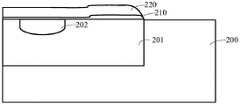
如图2A所示,提供半导体衬底200,半导体衬底200的构成材料可以采用未掺杂的单晶硅、掺杂有杂质的单晶硅、绝缘体上硅(SOI)、绝缘体上层叠硅(SSOI)、绝缘体上层叠锗化硅(S-SiGeOI)、绝缘体上锗化硅(SiGeOI)以及绝缘体上锗(GeOI)等。在本实施例中,半导体衬底200的构成材料选用P型半导体衬底200。As shown in FIG. 2A , a
在一个实施例中,氧化半导体衬底200,形成缓冲层(氧化硅层,图未示),在缓冲层上淀积氮化硅层,通过光刻定义出阱区201,并通过反应离子刻蚀氧化硅层,通过离子注入的方式在半导体衬底200中先注入磷P+,后注砷As+形成N型阱区201。在其他实施例中,其半导体衬底的导电类型,与位于半导体衬底200中阱区201的导电类型可以根据实际需求来设定,并不限于此。In one embodiment, the
在一个实施例中,还在阱区201内通过离子注入或其他方式形成沟道区202。In one embodiment, a
在一个实施例中,在半导体衬底200上用热氧化或者化学氧化工艺形成栅氧化层210。In one embodiment, the
具体地,所述栅氧化层210包括在竖直方向对应源区的第一栅氧化层211区域和在竖直方向对应漏区的第二栅氧化层213区域;其中,第一栅氧化层211区域的厚度小于所述第二栅氧化层213区域的厚度。Specifically, the
进一步地,第一栅氧化层211区域的厚度为15nm,第二栅氧化层213区域的厚度为44nm,由于第二栅氧化层213的厚度高于第一栅氧化层211的厚度,可以提供漏区的电压。通过在不同的区域形成不同厚度的栅氧化层210,可以形成高压金属氧化物半导体场效应晶体管(Metal Oxide Semiconductor,MOS)器件。Further, the thickness of the first
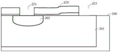
如图2B所示,半导体器件的制备方法还包括在栅氧化层210上形成多晶硅层220的步骤,其中,形成多晶硅层220的方法可以采用化学气相沉积法,如低温化学气相沉积、低压化学气相沉积、快热化学气相沉积等离子体增强化学气相沉积。As shown in FIG. 2B , the preparation method of the semiconductor device further includes the step of forming a
具体地,多晶硅层220的厚度为180~220nm,在本实施例中,多晶硅层220的厚度为2 00nm。Specifically, the thickness of the
步骤S120:刻蚀部分所述栅氧化层和多晶硅层并露出用于形成源区的第一开口和用于形成漏区的第二开口。Step S120: Etching a portion of the gate oxide layer and the polysilicon layer to expose a first opening for forming a source region and a second opening for forming a drain region.
如图2C所示,同时刻蚀部分栅氧化层210和多晶硅层220,刻蚀形成第一开口221和第二开口223。其中,第一开口221的底面为部分沟道区202的顶面,第一开口221可以定义后续形成源区侧墙以及源区的位置,第二开口223与第一开口221隔离设置,且第二开口223的底面为阱区201的顶面,第二开口223可以定义后续形成漏区侧墙以及漏区的位置。As shown in FIG. 2C , part of the
形成第一开口221和第二开口223的工艺步骤包括:在多晶硅层220上形成具有第一开口221和第二开口223图案的掩膜层,可以采用常规的光刻、刻蚀工艺形成掩膜层,掩膜层可以为单层结构或多层结构,具有单层结构的掩膜层为图案化的光刻胶层,具有多层结构的掩膜层可以包括自下而上层叠的图案化的先进图案化层、抗反射涂层和光刻胶层;以掩膜层为掩膜,同时蚀刻栅氧化层210和多晶硅层220,在栅氧化层210和多晶硅层220形成第一开口221和第二开口223,蚀刻可以是常规的各向异性的干法蚀刻;去除掩膜层,可以采用常规的灰化工艺去除掩膜层;实施湿法清洗,以去除蚀刻所产生的副产物和杂质。The process steps of forming the
在一个实施例中,其阱区201内的沟道区202也可以在形成第一开口221后,从第一开口221通过离子注入的方式形成。In one embodiment, the
步骤S130:在所述多晶硅层上、第一开口内、第二开口内依次形成第一介质层和第二介质层,并在所述第一开口的侧壁形成源区侧墙,在所述第二开口的侧壁形成漏区侧墙。Step S130 : sequentially forming a first dielectric layer and a second dielectric layer on the polysilicon layer, in the first opening, and in the second opening, and forming a source region spacer on the sidewall of the first opening, The sidewalls of the second openings form drain sidewalls.
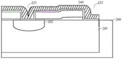
如图2D所示,在一个实施例中,在多晶硅层220、第一开口221、第二开口223形成第一介质层230,其中,第一介质层230形成于第一开口221的侧壁、底面,第一介质层230形成于第二开口223的侧壁、底面,但未填满第一开口221和第二开口223。As shown in FIG. 2D , in one embodiment, a first
如图2E所示,进一步地,在第一介质层230的基础上,形成第二介质层240。其中,第二介质层240的厚度大于第一介质层230的厚度。形成第一介质层230和第二介质层240的方法可以采用化学气相沉积法,如低温化学气相沉积、低压化学气相沉积、快热化学气相沉积等离子体增强化学气相沉积。As shown in FIG. 2E , further, on the basis of the
在一个实施例中,所述第一介质层230为氧化层,所述氧化层的厚度范围为8~12纳米。所述第二介质层240为氮化硅层;所述氮化硅层的厚度范围为80~120纳米。In one embodiment, the
如图2F所示,在一个实施例中,通过光刻、刻蚀等工艺刻蚀氮化硅层和氧化层,形成源区侧墙241和漏区侧墙243,除源区侧墙241和漏区侧墙243外的氮化硅层和氧化层,全部刻蚀去除露出多晶硅层220。相应的,第一开口221内的中间部分的氮化硅层和氧化层也被刻蚀至沟道区202,并露出部分沟道区202。第二开口223内的一部分的氮化硅层和氧化层刻蚀至阱区201,并露出阱区201。蚀刻可以是各向异性的干法蚀刻或/和湿法刻蚀。As shown in FIG. 2F , in one embodiment, the silicon nitride layer and the oxide layer are etched through processes such as photolithography, etching, etc. to form the
步骤S140:在所述多晶硅层上形成介质氧化层,刻蚀并保留位于所述漏区侧墙上的所述介质氧化层。Step S140 : forming a dielectric oxide layer on the polysilicon layer, etching and retaining the dielectric oxide layer on the sidewall of the drain region.
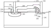
如图2G所示,在多晶硅层220上通过淀积形成介质氧化层250,其中,介质氧化层250还形成于源区侧墙241的侧壁、第一开口221的底部(沟道区202);介质氧化层250还形成于漏区侧墙243的侧壁、第二开口223的底部(阱区201)。As shown in FIG. 2G , a
如图2H所示,并在刻蚀介质氧化层250时,利用介质氧化层250的光刻版作为阻挡层保护漏区侧墙243不被刻掉。也即,漏区侧墙243上的介质氧化层250并未被刻蚀,漏区侧墙243包括氮化硅和氧化层双层结构,漏区侧墙243可以降低漏端的电场强度,有利于器件的击穿特性。其中,介质氧化层250可以为二氧化硅层。As shown in FIG. 2H , when the
步骤S150:去除所述源区侧墙中的第二介质层并保留所述第一介质层。Step S150: Remove the second dielectric layer in the source spacer and keep the first dielectric layer.
如图2I所示,在介质氧化层250刻蚀之后,利用湿法漂洗,将源区(带有沟道区202一端)侧墙241的第二介质层240(氮化硅层)漂掉,使得源区侧墙241中的介质层只有第一介质层230(氧化层)一层介质。也即,在不改变漏区结构的前提下,实现了源区侧墙241的横向厚度(也可以称之为第一介质层230的厚度)相对于漏区侧墙243的横向厚度的减小,缩短了源区所对应的多晶硅层220的间距,即可减小整个半导体器件的尺寸,降低了半导体器件的导通电阻。As shown in FIG. 2I, after the
通过上述半导体器件的制备方法,可以减少了源端侧墙的横向厚度,缩短了源区所对应的多晶硅层220的间距,即可减小整个半导体器件的尺寸,降低了半导体器件的导通电阻。同时利用现有的阻挡层保留了漏区侧墙243中双层介质层,降低了工艺成本,同时又能够保证漏区电场不发生变化,不会影响半导体器件的原有特性。Through the above-mentioned preparation method of the semiconductor device, the lateral thickness of the sidewall at the source end can be reduced, the spacing of the
在一个实施例中,在步骤S140,在所述多晶硅层220上形成介质氧化层250前,半导体器件的制备方法还包括在所述阱区201内形成所述源区203和漏区204的步骤。In one embodiment, in step S140 , before forming the
如图2G所示,在一个实施例中,半导体器件的制造方法还包括通过磷离子或砷离子注入工艺在半导体衬底中形成源区203和漏区204。由于半导体衬底中的源区203、沟道区202均在步骤S150之前形成,因此不会影响源区的杂质分布。As shown in FIG. 2G , in one embodiment, the method for fabricating a semiconductor device further includes forming a
在一个实施例中,在步骤S150,去除所述源区侧墙中的第二介质层并保留所述第一介质层的步骤后,还包括在所述多晶硅层上形成层间介质层;以及在所述层间介质层中形成接触孔的步骤。In one embodiment, in step S150, after the step of removing the second dielectric layer in the source spacer and retaining the first dielectric layer, the method further includes forming an interlayer dielectric layer on the polysilicon layer; and The step of forming contact holes in the interlayer dielectric layer.
如图2J所示,在一个实施例中,半导体器件的制造方法还包括在半导体衬底上形成第一层间介质层260和第二层间介质层270。作为示例,第一层间介质层260和第二层间介质层270的材料具有低介电常数的材料,所述具有低介电常数的材料包括但不限于k值为2.5-2.9的硅酸盐化合物(Hydrogen Silsesquioxane,简称为HSQ)、k值为2.2的甲基硅酸盐化合物(Methyl Silsesquioxane,简称MSQ)、以及化学气相沉积方法形成的多孔性二氧化硅等等。第一层间介质层260和第二层间介质层270的形成方法可以采用化学气相沉积法,如低温化学气相沉积、低压化学气相沉积、快热化学气相沉积、等离子体增强化学气相沉积等。如图2J所示,在一个实施例中,半导体器件的制造方法还包括通过光刻、刻蚀工艺形成贯穿第一层间介质层260和第二层间介质层270的接触孔261。作为示例,在第二层间介质层270上形成具有接触孔261图案的掩膜层,以该掩膜层为掩膜,蚀刻第一层间介质层260和第二层间介质层270,在第一层间介质层260和第二层间介质层270中形成露出源区203和漏区204的接触孔261,去除该掩膜层后,在所述通孔中填充金属层,以形成金属连接线。As shown in FIG. 2J , in one embodiment, the method for fabricating a semiconductor device further includes forming a first
传统的漏区侧墙中包括第一介质层和第二介质层(氮化硅层),在形成接触孔时,腐蚀到漏区侧墙的氮化硅时,其氮化硅层被腐蚀的速率较低,可能会造成接触孔不能刻蚀贯穿至源区,为了防止接触孔刻蚀出现异常,需要限定接触孔与氮化硅层之间的安全距离。也即,在形成接触孔261时,应确保其接触孔261不会与源区侧墙241中的第二介质层240(氮化硅层)、漏区侧墙243中的第二介质层240(氮化硅层)接触,需要保证接触孔261到多晶硅层220的距离大于源区侧墙241或漏区侧墙243的宽度。由于源区侧墙241中的第二介质层240(氮化硅层)被漂掉,其源区侧墙241的宽度越小,接触孔261到多晶硅层220的距离也就越小,多晶硅层220的间距也就越小。The traditional drain spacer includes a first dielectric layer and a second dielectric layer (silicon nitride layer). When the contact hole is formed, when the silicon nitride of the drain spacer is etched, the silicon nitride layer is etched. If the rate is low, the contact hole may not be etched through to the source region. In order to prevent abnormal etching of the contact hole, a safe distance between the contact hole and the silicon nitride layer needs to be defined. That is, when the
通过上述方法制备的半导体器件可以为N型MOS管、P型MOS管、高压MOS管等。通过上述半导体器件的制备方法,可以减少了源端侧墙的横向厚度,缩短了源区所对应的多晶硅层220的间距,即可减小整个半导体器件的尺寸,降低了半导体器件的导通电阻。同时利用现有的阻挡层保留了漏区侧墙243中双层介质层,降低了工艺成本,同时又能够保证漏区电场不发生变化,不会影响半导体器件的原有特性。The semiconductor device prepared by the above method can be an N-type MOS transistor, a P-type MOS transistor, a high-voltage MOS transistor, or the like. Through the above-mentioned preparation method of the semiconductor device, the lateral thickness of the sidewall at the source end can be reduced, the spacing of the
此外,还提供一种半导体器件,如图2J所示,半导体器件包括:半导体衬底(图未示),所述半导体内设有阱区201以及位于所述阱区201内的沟道区202;位于所述半导体衬底上的栅氧化层210和多晶硅层220,以及设置在所述栅氧化层210和多晶硅层220上的用于形成源区203的第一开口(图未标)和用于形成漏区204的第二开口(图未标);位于所述第一开口侧壁的源区侧墙241和位于所述第二开口侧壁的漏区侧墙243,其中,所述源区侧墙241包括所述第一介质层230,所述漏区侧墙243包括依次层叠的第一介质层230、第二介质层240;以及位于所述漏区侧墙243上的介质氧化层250。In addition, a semiconductor device is also provided. As shown in FIG. 2J , the semiconductor device includes: a semiconductor substrate (not shown), in which a
在一个实施例中,所述第一介质层230为氧化层,所述第二介质层240为氮化硅层。In one embodiment, the
具体地,所述氧化层的厚度范围为8~12纳米;所述氮化硅层的厚度范围为80~120纳米。Specifically, the thickness of the oxide layer ranges from 8 to 12 nanometers; the thickness of the silicon nitride layer ranges from 80 to 120 nanometers.
在一个实施例中,半导体器件还包括位于阱区201内的源区203和漏区204,源区203和漏区204的形成是通过磷离子或砷离子注入工艺而形成的。其中,源区与第一开口对应设置,漏区与第二开口对应设置。In one embodiment, the semiconductor device further includes a
在一个实施例中,半导体器件还包括位于所述多晶硅层220上的层间介质层260,以及位于所述层间介质层260中的接触孔261。In one embodiment, the semiconductor device further includes an
层间介质层260的材料优选具有低介电常数的材料,所述具有低介电常数的材料包括但不限于k值为2.5-2.9的硅酸盐化合物(Hydrogen Silsesquioxane,简称为HSQ)、k值为2.2的甲基硅酸盐化合物(Methyl Silsesquioxane,简称MSQ)、以及化学气相沉积方法形成的多孔性二氧化硅等等。层间介质层260的形成方法可以采用化学气相沉积法,如低温化学气相沉积、低压化学气相沉积、快热化学气相沉积、等离子体增强化学气相沉积等。通过光刻、刻蚀工艺形成贯穿层间介质层260的接触孔261。作为示例,在层间介质层260上形成具有接触孔261图案的掩膜层,以该掩膜层为掩膜,蚀刻层间介质层260,在层间介质层260中形成露出阱区201的通孔,去除该掩膜层后,在所述通孔中填充金属层,以形成金属连接线。在形成接触孔261时,应确保其接触孔261不会与源区侧墙241、漏区侧墙243接触,需要保证接触孔261到多晶硅层220的距离大于源区侧墙241或漏区侧墙243的宽度。其源区侧墙241或漏区侧墙243的宽度越小,接触孔261到多晶硅层220的距离也就越小,多晶硅层220的间距也就越小。The material of the
半导体器件可以为N型MOS管、P型MOS管、高压MOS管等。上述半导体器件,减少了源端侧墙的横向厚度,缩短了源区所对应的多晶硅层220的间距,即可减小整个半导体器件的尺寸,降低了半导体器件的导通电阻。同时利用现有的阻挡层保留了漏区侧墙中双层介质层,降低了工艺成本,同时又能够保证漏区电场不发生变化,不会影响半导体器件的原有特性。The semiconductor device may be an N-type MOS transistor, a P-type MOS transistor, a high-voltage MOS transistor, or the like. In the above semiconductor device, the lateral thickness of the source sidewall spacer is reduced, and the distance between the polysilicon layers 220 corresponding to the source region is shortened, which can reduce the size of the entire semiconductor device and reduce the on-resistance of the semiconductor device. At the same time, the existing barrier layer is used to retain the double-layer dielectric layer in the sidewall of the drain region, which reduces the process cost, and at the same time, it can ensure that the electric field of the drain region does not change, and the original characteristics of the semiconductor device are not affected.
以上所述实施例的各技术特征可以进行任意的组合,为使描述简洁,未对上述实施例中的各个技术特征所有可能的组合都进行描述,然而,只要这些技术特征的组合不存在矛盾,都应当认为是本说明书记载的范围。The technical features of the above-described embodiments can be combined arbitrarily. For the sake of brevity, all possible combinations of the technical features in the above-described embodiments are not described. However, as long as there is no contradiction between the combinations of these technical features, All should be regarded as the scope described in this specification.
以上所述实施例仅表达了本发明的几种实施方式,其描述较为具体和详细,但并不能因此而理解为对发明专利范围的限制。应当指出的是,对于本领域的普通技术人员来说,在不脱离本发明构思的前提下,还可以做出若干变形和改进,这些都属于本发明的保护范围。因此,本发明专利的保护范围应以所附权利要求为准。The above-mentioned embodiments only represent several embodiments of the present invention, and the descriptions thereof are specific and detailed, but should not be construed as a limitation on the scope of the invention patent. It should be pointed out that for those of ordinary skill in the art, without departing from the concept of the present invention, several modifications and improvements can also be made, which all belong to the protection scope of the present invention. Therefore, the protection scope of the patent of the present invention should be subject to the appended claims.
Claims (10)
Priority Applications (3)
| Application Number | Priority Date | Filing Date | Title |
|---|---|---|---|
| CN201710534707.4ACN109216193B (en) | 2017-07-03 | 2017-07-03 | Semiconductor device and method of making the same |
| US16/462,432US10811520B2 (en) | 2017-07-03 | 2018-07-03 | Semiconductor device and method for manufacturing same |
| PCT/CN2018/094316WO2019007335A1 (en) | 2017-07-03 | 2018-07-03 | Semiconductor device and method for manufacturing same |
Applications Claiming Priority (1)
| Application Number | Priority Date | Filing Date | Title |
|---|---|---|---|
| CN201710534707.4ACN109216193B (en) | 2017-07-03 | 2017-07-03 | Semiconductor device and method of making the same |
Publications (2)
| Publication Number | Publication Date |
|---|---|
| CN109216193A CN109216193A (en) | 2019-01-15 |
| CN109216193Btrue CN109216193B (en) | 2021-08-20 |
Family
ID=64949694
Family Applications (1)
| Application Number | Title | Priority Date | Filing Date |
|---|---|---|---|
| CN201710534707.4AActiveCN109216193B (en) | 2017-07-03 | 2017-07-03 | Semiconductor device and method of making the same |
Country Status (3)
| Country | Link |
|---|---|
| US (1) | US10811520B2 (en) |
| CN (1) | CN109216193B (en) |
| WO (1) | WO2019007335A1 (en) |
Families Citing this family (3)
| Publication number | Priority date | Publication date | Assignee | Title |
|---|---|---|---|---|
| CN112820645B (en)* | 2020-12-31 | 2022-07-05 | 北京燕东微电子科技有限公司 | Power semiconductor device and preparation method thereof |
| CN112993159A (en)* | 2021-02-05 | 2021-06-18 | 上海华虹宏力半导体制造有限公司 | Preparation method of passive integrated device |
| US11913188B2 (en) | 2021-02-11 | 2024-02-27 | R.H. Borden And Company, Llc | Automated tool access to a manhole through automated manhole cover removal using self-driving vehicle |
Citations (8)
| Publication number | Priority date | Publication date | Assignee | Title |
|---|---|---|---|---|
| US5489546A (en)* | 1995-05-24 | 1996-02-06 | Micron Technology, Inc. | Method of forming CMOS devices using independent thickness spacers in a split-polysilicon DRAM process |
| US5789298A (en)* | 1996-11-04 | 1998-08-04 | Advanced Micro Devices, Inc. | High performance mosfet structure having asymmetrical spacer formation and method of making the same |
| US5950091A (en)* | 1996-12-06 | 1999-09-07 | Advanced Micro Devices, Inc. | Method of making a polysilicon gate conductor of an integrated circuit formed as a sidewall spacer on a sacrificial material |
| CN101719512A (en)* | 2009-11-26 | 2010-06-02 | 上海宏力半导体制造有限公司 | High-voltage transistor and manufacturing method thereof |
| CN101752251A (en)* | 2008-12-04 | 2010-06-23 | 上海华虹Nec电子有限公司 | Fully-automatic aligning high-pressure N-shaped DMOS device and manufacturing method thereof |
| US7892928B2 (en)* | 2007-03-23 | 2011-02-22 | International Business Machines Corporation | Method of forming asymmetric spacers and methods of fabricating semiconductor device using asymmetric spacers |
| CN102544095A (en)* | 2010-12-24 | 2012-07-04 | 中国科学院微电子研究所 | Mos transistor and manufacturing method thereof |
| CN103811496A (en)* | 2012-11-01 | 2014-05-21 | 台湾积体电路制造股份有限公司 | Method and apparatus for non-volatile memory cells with increased programming efficiency |
Family Cites Families (4)
| Publication number | Priority date | Publication date | Assignee | Title |
|---|---|---|---|---|
| KR100487951B1 (en)* | 2003-02-11 | 2005-05-06 | 삼성전자주식회사 | A semiconductor device having self-aligned contact hole and fabrication method thereof |
| US8072035B2 (en)* | 2007-06-11 | 2011-12-06 | Renesas Electronics Corporation | Semiconductor device and method of manufacturing the same |
| US20090159936A1 (en)* | 2007-12-20 | 2009-06-25 | Uday Shah | Device with asymmetric spacers |
| CN106328523B (en)* | 2015-06-15 | 2019-10-15 | 北大方正集团有限公司 | Fabrication method of radio frequency lateral double diffused MOS device |
- 2017
- 2017-07-03CNCN201710534707.4Apatent/CN109216193B/enactiveActive
- 2018
- 2018-07-03WOPCT/CN2018/094316patent/WO2019007335A1/ennot_activeCeased
- 2018-07-03USUS16/462,432patent/US10811520B2/enactiveActive
Patent Citations (8)
| Publication number | Priority date | Publication date | Assignee | Title |
|---|---|---|---|---|
| US5489546A (en)* | 1995-05-24 | 1996-02-06 | Micron Technology, Inc. | Method of forming CMOS devices using independent thickness spacers in a split-polysilicon DRAM process |
| US5789298A (en)* | 1996-11-04 | 1998-08-04 | Advanced Micro Devices, Inc. | High performance mosfet structure having asymmetrical spacer formation and method of making the same |
| US5950091A (en)* | 1996-12-06 | 1999-09-07 | Advanced Micro Devices, Inc. | Method of making a polysilicon gate conductor of an integrated circuit formed as a sidewall spacer on a sacrificial material |
| US7892928B2 (en)* | 2007-03-23 | 2011-02-22 | International Business Machines Corporation | Method of forming asymmetric spacers and methods of fabricating semiconductor device using asymmetric spacers |
| CN101752251A (en)* | 2008-12-04 | 2010-06-23 | 上海华虹Nec电子有限公司 | Fully-automatic aligning high-pressure N-shaped DMOS device and manufacturing method thereof |
| CN101719512A (en)* | 2009-11-26 | 2010-06-02 | 上海宏力半导体制造有限公司 | High-voltage transistor and manufacturing method thereof |
| CN102544095A (en)* | 2010-12-24 | 2012-07-04 | 中国科学院微电子研究所 | Mos transistor and manufacturing method thereof |
| CN103811496A (en)* | 2012-11-01 | 2014-05-21 | 台湾积体电路制造股份有限公司 | Method and apparatus for non-volatile memory cells with increased programming efficiency |
Also Published As
| Publication number | Publication date |
|---|---|
| US20190378912A1 (en) | 2019-12-12 |
| WO2019007335A1 (en) | 2019-01-10 |
| US10811520B2 (en) | 2020-10-20 |
| CN109216193A (en) | 2019-01-15 |
Similar Documents
| Publication | Publication Date | Title |
|---|---|---|
| TWI662627B (en) | Semiconductor device and method of forming same | |
| CN102104003B (en) | Method for manufacturing semiconductor device | |
| US8889497B2 (en) | Semiconductor devices and methods of manufacture thereof | |
| CN112563266A (en) | Semiconductor device with a plurality of semiconductor chips | |
| TWI511292B (en) | Method of forming a fin field effect transistor device having an alternative channel material | |
| CN109904120A (en) | Semiconductor device and method of manufacturing the same | |
| JP2010537433A (en) | Method for manufacturing adjacent silicon fins of different heights | |
| WO2018040865A1 (en) | Vdmos device and manufacturing method therefor | |
| WO2014071653A1 (en) | Semiconductor device and manufacturing method therefor | |
| WO2014071659A1 (en) | Semiconductor device and manufacturing method therefor | |
| CN106952816B (en) | Method of forming a fin transistor | |
| CN104517901A (en) | Method for forming CMOS transistor | |
| TW201913751A (en) | Semiconductor component and method of forming same | |
| CN110504162B (en) | Area Selective Deposition of Masking Materials | |
| WO2018040866A1 (en) | Vdmos device and manufacturing method therefor | |
| CN109216193B (en) | Semiconductor device and method of making the same | |
| WO2013000197A1 (en) | Semiconductor structure and manufacturing method thereof | |
| TWI767417B (en) | Semiconductor device and manufacturing method thereof | |
| CN107452680B (en) | Semiconductor device and method of manufacturing the same | |
| US10312150B1 (en) | Protected trench isolation for fin-type field-effect transistors | |
| CN109841507B (en) | Semiconductor device and method of forming the same | |
| CN103531476B (en) | Semiconductor device manufacturing method | |
| CN109887845B (en) | Semiconductor device and method of forming the same | |
| CN103839792B (en) | Semiconductor device manufacturing method | |
| CN110534479B (en) | Grid electrode for improving filling capability of dielectric layer in zero layer and process method |
Legal Events
| Date | Code | Title | Description |
|---|---|---|---|
| PB01 | Publication | ||
| PB01 | Publication | ||
| SE01 | Entry into force of request for substantive examination | ||
| SE01 | Entry into force of request for substantive examination | ||
| GR01 | Patent grant | ||
| GR01 | Patent grant |