CN109213361B - Micro LED Display Panel - Google Patents
Micro LED Display PanelDownload PDFInfo
- Publication number
- CN109213361B CN109213361BCN201810524449.6ACN201810524449ACN109213361BCN 109213361 BCN109213361 BCN 109213361BCN 201810524449 ACN201810524449 ACN 201810524449ACN 109213361 BCN109213361 BCN 109213361B
- Authority
- CN
- China
- Prior art keywords
- layer
- micro led
- display panel
- led display
- transparent conductive
- Prior art date
- Legal status (The legal status is an assumption and is not a legal conclusion. Google has not performed a legal analysis and makes no representation as to the accuracy of the status listed.)
- Active
Links
Images


Classifications
- G—PHYSICS
- G09—EDUCATION; CRYPTOGRAPHY; DISPLAY; ADVERTISING; SEALS
- G09G—ARRANGEMENTS OR CIRCUITS FOR CONTROL OF INDICATING DEVICES USING STATIC MEANS TO PRESENT VARIABLE INFORMATION
- G09G3/00—Control arrangements or circuits, of interest only in connection with visual indicators other than cathode-ray tubes
- G09G3/20—Control arrangements or circuits, of interest only in connection with visual indicators other than cathode-ray tubes for presentation of an assembly of a number of characters, e.g. a page, by composing the assembly by combination of individual elements arranged in a matrix no fixed position being assigned to or needed to be assigned to the individual characters or partial characters
- G09G3/22—Control arrangements or circuits, of interest only in connection with visual indicators other than cathode-ray tubes for presentation of an assembly of a number of characters, e.g. a page, by composing the assembly by combination of individual elements arranged in a matrix no fixed position being assigned to or needed to be assigned to the individual characters or partial characters using controlled light sources
- G09G3/30—Control arrangements or circuits, of interest only in connection with visual indicators other than cathode-ray tubes for presentation of an assembly of a number of characters, e.g. a page, by composing the assembly by combination of individual elements arranged in a matrix no fixed position being assigned to or needed to be assigned to the individual characters or partial characters using controlled light sources using electroluminescent panels
- G09G3/32—Control arrangements or circuits, of interest only in connection with visual indicators other than cathode-ray tubes for presentation of an assembly of a number of characters, e.g. a page, by composing the assembly by combination of individual elements arranged in a matrix no fixed position being assigned to or needed to be assigned to the individual characters or partial characters using controlled light sources using electroluminescent panels semiconductive, e.g. using light-emitting diodes [LED]
- G—PHYSICS
- G06—COMPUTING OR CALCULATING; COUNTING
- G06F—ELECTRIC DIGITAL DATA PROCESSING
- G06F3/00—Input arrangements for transferring data to be processed into a form capable of being handled by the computer; Output arrangements for transferring data from processing unit to output unit, e.g. interface arrangements
- G06F3/01—Input arrangements or combined input and output arrangements for interaction between user and computer
- G06F3/03—Arrangements for converting the position or the displacement of a member into a coded form
- G06F3/041—Digitisers, e.g. for touch screens or touch pads, characterised by the transducing means
- G06F3/0412—Digitisers structurally integrated in a display
- G—PHYSICS
- G06—COMPUTING OR CALCULATING; COUNTING
- G06F—ELECTRIC DIGITAL DATA PROCESSING
- G06F1/00—Details not covered by groups G06F3/00 - G06F13/00 and G06F21/00
- G06F1/16—Constructional details or arrangements
- G06F1/1613—Constructional details or arrangements for portable computers
- G06F1/1633—Constructional details or arrangements of portable computers not specific to the type of enclosures covered by groups G06F1/1615 - G06F1/1626
- G06F1/1637—Details related to the display arrangement, including those related to the mounting of the display in the housing
- G06F1/1643—Details related to the display arrangement, including those related to the mounting of the display in the housing the display being associated to a digitizer, e.g. laptops that can be used as penpads
- G—PHYSICS
- G06—COMPUTING OR CALCULATING; COUNTING
- G06F—ELECTRIC DIGITAL DATA PROCESSING
- G06F3/00—Input arrangements for transferring data to be processed into a form capable of being handled by the computer; Output arrangements for transferring data from processing unit to output unit, e.g. interface arrangements
- G06F3/01—Input arrangements or combined input and output arrangements for interaction between user and computer
- G06F3/03—Arrangements for converting the position or the displacement of a member into a coded form
- G06F3/041—Digitisers, e.g. for touch screens or touch pads, characterised by the transducing means
- G06F3/0416—Control or interface arrangements specially adapted for digitisers
- G—PHYSICS
- G06—COMPUTING OR CALCULATING; COUNTING
- G06F—ELECTRIC DIGITAL DATA PROCESSING
- G06F3/00—Input arrangements for transferring data to be processed into a form capable of being handled by the computer; Output arrangements for transferring data from processing unit to output unit, e.g. interface arrangements
- G06F3/01—Input arrangements or combined input and output arrangements for interaction between user and computer
- G06F3/03—Arrangements for converting the position or the displacement of a member into a coded form
- G06F3/041—Digitisers, e.g. for touch screens or touch pads, characterised by the transducing means
- G06F3/044—Digitisers, e.g. for touch screens or touch pads, characterised by the transducing means by capacitive means
- G—PHYSICS
- G09—EDUCATION; CRYPTOGRAPHY; DISPLAY; ADVERTISING; SEALS
- G09F—DISPLAYING; ADVERTISING; SIGNS; LABELS OR NAME-PLATES; SEALS
- G09F9/00—Indicating arrangements for variable information in which the information is built-up on a support by selection or combination of individual elements
- G09F9/30—Indicating arrangements for variable information in which the information is built-up on a support by selection or combination of individual elements in which the desired character or characters are formed by combining individual elements
- G09F9/33—Indicating arrangements for variable information in which the information is built-up on a support by selection or combination of individual elements in which the desired character or characters are formed by combining individual elements being semiconductor devices, e.g. diodes
- H—ELECTRICITY
- H01—ELECTRIC ELEMENTS
- H01L—SEMICONDUCTOR DEVICES NOT COVERED BY CLASS H10
- H01L25/00—Assemblies consisting of a plurality of semiconductor or other solid state devices
- H01L25/03—Assemblies consisting of a plurality of semiconductor or other solid state devices all the devices being of a type provided for in a single subclass of subclasses H10B, H10D, H10F, H10H, H10K or H10N, e.g. assemblies of rectifier diodes
- H01L25/04—Assemblies consisting of a plurality of semiconductor or other solid state devices all the devices being of a type provided for in a single subclass of subclasses H10B, H10D, H10F, H10H, H10K or H10N, e.g. assemblies of rectifier diodes the devices not having separate containers
- H01L25/075—Assemblies consisting of a plurality of semiconductor or other solid state devices all the devices being of a type provided for in a single subclass of subclasses H10B, H10D, H10F, H10H, H10K or H10N, e.g. assemblies of rectifier diodes the devices not having separate containers the devices being of a type provided for in group H10H20/00
- H01L25/0753—Assemblies consisting of a plurality of semiconductor or other solid state devices all the devices being of a type provided for in a single subclass of subclasses H10B, H10D, H10F, H10H, H10K or H10N, e.g. assemblies of rectifier diodes the devices not having separate containers the devices being of a type provided for in group H10H20/00 the devices being arranged next to each other
- G—PHYSICS
- G06—COMPUTING OR CALCULATING; COUNTING
- G06F—ELECTRIC DIGITAL DATA PROCESSING
- G06F2203/00—Indexing scheme relating to G06F3/00 - G06F3/048
- G06F2203/041—Indexing scheme relating to G06F3/041 - G06F3/045
- G06F2203/04112—Electrode mesh in capacitive digitiser: electrode for touch sensing is formed of a mesh of very fine, normally metallic, interconnected lines that are almost invisible to see. This provides a quite large but transparent electrode surface, without need for ITO or similar transparent conductive material
- G—PHYSICS
- G09—EDUCATION; CRYPTOGRAPHY; DISPLAY; ADVERTISING; SEALS
- G09G—ARRANGEMENTS OR CIRCUITS FOR CONTROL OF INDICATING DEVICES USING STATIC MEANS TO PRESENT VARIABLE INFORMATION
- G09G2300/00—Aspects of the constitution of display devices
- G09G2300/04—Structural and physical details of display devices
- G09G2300/0421—Structural details of the set of electrodes
- G09G2300/0426—Layout of electrodes and connections
- H—ELECTRICITY
- H01—ELECTRIC ELEMENTS
- H01L—SEMICONDUCTOR DEVICES NOT COVERED BY CLASS H10
- H01L25/00—Assemblies consisting of a plurality of semiconductor or other solid state devices
- H01L25/16—Assemblies consisting of a plurality of semiconductor or other solid state devices the devices being of types provided for in two or more different subclasses of H10B, H10D, H10F, H10H, H10K or H10N, e.g. forming hybrid circuits
- H01L25/167—Assemblies consisting of a plurality of semiconductor or other solid state devices the devices being of types provided for in two or more different subclasses of H10B, H10D, H10F, H10H, H10K or H10N, e.g. forming hybrid circuits comprising optoelectronic devices, e.g. LED, photodiodes
- H—ELECTRICITY
- H10—SEMICONDUCTOR DEVICES; ELECTRIC SOLID-STATE DEVICES NOT OTHERWISE PROVIDED FOR
- H10H—INORGANIC LIGHT-EMITTING SEMICONDUCTOR DEVICES HAVING POTENTIAL BARRIERS
- H10H20/00—Individual inorganic light-emitting semiconductor devices having potential barriers, e.g. light-emitting diodes [LED]
- H10H20/80—Constructional details
- H10H20/85—Packages
- H10H20/857—Interconnections, e.g. lead-frames, bond wires or solder balls
Landscapes
- Engineering & Computer Science (AREA)
- Theoretical Computer Science (AREA)
- General Engineering & Computer Science (AREA)
- Physics & Mathematics (AREA)
- General Physics & Mathematics (AREA)
- Human Computer Interaction (AREA)
- Computer Hardware Design (AREA)
- Power Engineering (AREA)
- Microelectronics & Electronic Packaging (AREA)
- Condensed Matter Physics & Semiconductors (AREA)
- Devices For Indicating Variable Information By Combining Individual Elements (AREA)
Abstract
Translated fromChinese
Description
Translated fromChinese技术领域technical field
本发明涉及显示技术领域,尤其涉及一种微型LED显示面板。The present invention relates to the field of display technology, in particular to a micro LED display panel.
背景技术Background technique
Micro-LED(Micro Light Emitting Display),也称为微型LED或μLED,是一种新兴的平板显示器技术。目前微型LED显示面板,其通常包括层叠设置的N型掺杂的无机发光材料层和P型掺杂的无机发光材料层、连接所述N型掺杂的无机发光材料层的透明导电膜层(作为阴极)、连接所述P型掺杂的无机发光材料层的金属层(作为阳极)。然而,目前的微型LED显示面板通常未设置有内嵌式(in-cell)的触控感测电极。Micro-LED (Micro Light Emitting Display), also known as micro LED or μLED, is an emerging flat panel display technology. At present, a micro LED display panel usually includes a layered N-type doped inorganic light-emitting material layer and a P-type doped inorganic light-emitting material layer, and a transparent conductive film layer ( as cathode), a metal layer (as anode) connecting said P-doped phosphor layer. However, current micro LED display panels are generally not provided with in-cell touch sensing electrodes.
发明内容SUMMARY OF THE INVENTION
鉴于以上内容,本发明提供一种微型LED显示面板,其包括:In view of the above, the present invention provides a micro LED display panel, which includes:
依次层叠设置的透明导电层、微型LED层和第一金属层;The transparent conductive layer, the micro LED layer and the first metal layer are stacked in sequence;
所述微型LED层包括间隔设置的多个微型LED;The micro LED layer includes a plurality of micro LEDs arranged at intervals;
所述第一金属层包括间隔设置的多个第一金属单元,所述多个第一金属单元作为所述多个微型LED的阳极;The first metal layer includes a plurality of first metal units arranged at intervals, and the plurality of first metal units serve as anodes of the plurality of micro LEDs;
所述透明导电层包括间隔设置的多个透明导电单元,所述多个透明导电单元作为所述多个微型LED的阴极并复用为触控电极。The transparent conductive layer includes a plurality of transparent conductive units arranged at intervals, and the plurality of transparent conductive units serve as the cathodes of the plurality of micro LEDs and are multiplexed as touch electrodes.
本发明实施例的微型LED显示面板,多个透明导电单元作为所述多个微型LED的阴极并复用为触控电极。通过采用分时驱动的方式将多个所述透明导电单元交替作为微型LED的阴极和微型LED显示面板的触控电极。在显示时间段,多个透明导电单元被输入直流电压信号,使得各微型LED发光,以用于显示画面;在触控时间段,多个透明导电单元被输入交流电压信号,以实现触控功能。如此,本发明实施例的微型LED显示面板兼具有显示功能和触控功能。In the micro LED display panel of the embodiment of the present invention, a plurality of transparent conductive units are used as cathodes of the plurality of micro LEDs and are multiplexed into touch electrodes. A plurality of the transparent conductive units are alternately used as the cathode of the micro LED and the touch electrode of the micro LED display panel by adopting a time-sharing driving manner. During the display period, a DC voltage signal is input to a plurality of transparent conductive units, so that each micro LED emits light for displaying images; during the touch period, an AC voltage signal is input to the plurality of transparent conductive units to realize the touch function. . In this way, the micro LED display panel of the embodiment of the present invention has both a display function and a touch function.
附图说明Description of drawings
图1为本发明第一实施例的微型LED显示面板的剖面示意图。FIG. 1 is a schematic cross-sectional view of a micro LED display panel according to a first embodiment of the present invention.
图2A为本发明第一实施例的微型LED显示面板的另一剖面示意图。2A is another schematic cross-sectional view of the micro LED display panel according to the first embodiment of the present invention.
图2B为图2A所示的微型LED显示面板的透明导电单元和N型掺杂的无机非金属层在上基板上的投影图。FIG. 2B is a projection view of the transparent conductive unit and the N-type doped inorganic non-metallic layer of the micro LED display panel shown in FIG. 2A on the upper substrate.
图2C为图2A所示的微型LED显示面板的透明导电单元和第二金属单元在上基板上的投影图。FIG. 2C is a projection view of the transparent conductive unit and the second metal unit of the micro LED display panel shown in FIG. 2A on the upper substrate.
图3为本发明第一实施例的微型LED显示面板的平面示意图。3 is a schematic plan view of the micro LED display panel according to the first embodiment of the present invention.
图4A为本发明第一实施例的微型LED显示面板的触控单元的正面示意图。4A is a schematic front view of the touch unit of the micro LED display panel according to the first embodiment of the present invention.
图4B为图4A所示的微型LED显示面板的触控单元的背面示意图。FIG. 4B is a schematic view of the backside of the touch unit of the micro LED display panel shown in FIG. 4A .
图5为本发明第二实施例的微型LED显示面板的剖面示意图。5 is a schematic cross-sectional view of a micro LED display panel according to a second embodiment of the present invention.
图6为本发明第二实施例的微型LED显示面板的另一剖面示意图。6 is another schematic cross-sectional view of the micro LED display panel according to the second embodiment of the present invention.
图7为本发明第二实施例的微型LED显示面板的平面示意图。7 is a schematic plan view of a micro LED display panel according to a second embodiment of the present invention.
主要元件符号说明Description of main component symbols


如下具体实施方式将结合上述附图进一步说明本发明。The following specific embodiments will further illustrate the present invention in conjunction with the above drawings.
具体实施方式Detailed ways
本文所述的微型LED是指尺寸小于500μm的LED,更确切地说,是指尺寸大约在1μm~100μm的范围LED。The micro-LEDs mentioned herein refer to LEDs with a size of less than 500 μm, more precisely, LEDs with a size in the range of about 1 μm to 100 μm.
第一实施例first embodiment
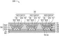
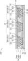
图1为本发明第一实施例的微型LED显示面板100的剖面示意图。如图1所示,该微型LED显示面板100,包括依次层叠设置的上基板10、透明导电层20、微型LED层30和第一金属层40。上基板10为透明的,透明导电层20包括间隔设置的多个透明导电单元211,微型LED层30包括间隔设置的多个微型LED31,第一金属层40包括间隔设置的多个第一金属单元41,所述多个第一金属单元41作为所述多个微型LED31的阳极,所述多个透明导电单元211作为所述多个微型LED31的阴极并复用为触控电极。FIG. 1 is a schematic cross-sectional view of a micro
请继续参阅图1,微型LED显示面板100包括多个子像素321,相邻的多个发不同颜色光的子像素321形成一个像素32。在本实施例中,每一个像素32包括三个相邻的子像素321,该三个相邻的子像素321分别为第一色子像素3211、第二色子像素3212及第三色子像素3213。其中,第一色子像素3211包括一个发红光的红色微型LED31,第二色子像素3212包括发绿光的绿色微型LED31,第三色子像素3213包括发蓝光的蓝色微型LED31。可以理解地,在本发明的其他实施例中,第一色子像素3211、第二色子像素3212及第三色子像素3213也可以分别包括发其他颜色光的微型LED31。Please continue to refer to FIG. 1 , the micro
可以理解地,在本发明的其他实施例中每一个像素32也可以包括三个以上相邻的子像素,比如相邻的四个所述子像素321形成一个像素32。该相邻的四个子像素321分别包括发红光的红色微型LED31、发绿光的绿色微型LED31、发蓝光的蓝色微型LED31和发白光的白色微型LED31。It can be understood that, in other embodiments of the present invention, each
请继续参阅图1,每一个子像素321包括一个微型LED31、层叠于微型LED31上方的一个透明导电单元211以及层叠于微型LED31下方的一个第一金属单元41。每一个微型LED31至少包括层叠设置的N型掺杂的无机非金属层311、P型掺杂的无机非金属层312、及设置在N型掺杂的无机非金属层311和P型掺杂的无机非金属层312之间的活性层(图未示)。通过调整微型LED31中的活性层材料,可以使微型LED31发不同颜色的光,从而使不同子像素321发不同颜色的光。Please continue to refer to FIG. 1 , each
请继续参阅图1,微型LED显示面板100还包括层叠设置的控制电路层70和下基板80,下基板80与上基板10相对设置,像素32及控制电路层70位于下基板80与上基板10之间。每一个第一金属单元41电性连接控制电路层70,并被控制电路层70施加电压信号。Please continue to refer to FIG. 1 , the micro
具体地,控制电路层70包括薄膜晶体管(TFT)阵列(图未示),下基板80为薄膜晶体管(TFT)阵列的绝缘承载基板,每个子像素321对应的第一金属单元41与一个薄膜晶体管(TFT)连接。此外,控制电路层70还包括一信号源(图未示),用于进行电源及控制信号的切换。具体地,该信号源可以为现场可编程门阵列(Field Programmable Gate Array,FPGA)、集成电路(IC)等等。Specifically, the
请继续参阅图1,微型LED显示面板100还包括层叠设置的异方性导电物质层50和第二金属层60,异方性导电物质层50包括间隔设置的多个异方性导电单元51,第二金属层60包括间隔设置的多个第二金属单元61。其中每一个透明导电单元211与一个微型LED31、一个第一金属单元41、一个异方性导电单元51和一个第二金属单元61为依次层叠设置。每一个异方性导电单元51用于电性连接一个第一金属单元41和一个第二金属单元61,每一个第二金属单元61位于一个异方性导电单元51和控制电路层70之间。如此设置,使得控制电路层70能够电性连接第一金属单元41,并通过第一金属单元41为其相对应的微型LED31提供直流电压信号。Please continue to refer to FIG. 1 , the micro
请继续参阅图1,微型LED显示面板100还包括多个绝缘结构90,绝缘结构90绝缘隔离多个透明导电单元211,绝缘隔离多个微型LED31,绝缘隔离多个第一金属单元41,绝缘隔离多个所述异方性导电单元51以及绝缘隔离多个所述第二金属单元61。Please continue to refer to FIG. 1, the micro
本实施例中,绝缘结构90包括第一钝化层902、第二钝化层903和第三钝化层904。其中,在制程中,将第一钝化层902、第二钝化层903形成于上基板10上以绝缘隔离多个所述子像素321,第三钝化层904形成于下基板80的控制电路层70上以绝缘隔离多个所述第二金属单元61,然后再通过异方性导电单元51将每一个第一金属单元41和每一个第二金属单元61绑定,以使控制电路层70能够电性连接每一个第一金属单元41,并通过多个第一金属单元41为其相对应的微型LED31提供电压信号。In this embodiment, the insulating
图2A为本发明第一实施例的微型LED显示面板100的另一剖面示意图,为了便于呈现的更加清楚,图2A中省略了控制电路层70和下基板80。如图2A所示,每一个第一金属单元41完全覆盖与其对应的P型掺杂的无机非金属层312,即,每一个第一金属单元41在上基板10上的投影完全覆盖与其对应的P型掺杂的无机非金属层312在上基板10上的投影。FIG. 2A is another schematic cross-sectional view of the micro
图2B为图2A所示的微型LED显示面板100的透明导电单元211和N型掺杂的无机非金属层311在上基板10上的投影图。如图2B所示,每一个透明导电单元211完全覆盖其对应的N型掺杂的无机非金属层311,即,每一个N型掺杂的无机非金属层311在上基板10上的投影完全位于其对应的透明导电单元211在所述上基板10上的投影之内。FIG. 2B is a projection view of the transparent
图2C为图2A所示的微型LED显示面板100的第一金属单元41和第二金属单元61在上基板上的投影图。请结合参阅图2A和图2C,透明导电单元211不覆盖N型掺杂的无机非金属层311的部分与一第二金属单元61电性接触。其中,每一个所述第二金属单元61电性连接控制电路层70,控制电路层70通过多个所述第二金属单元61电性连接透明导电单元211。FIG. 2C is a projection view of the
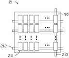
图3为本发明第一实施例的微型LED显示面板100的平面示意图。如图3所示,所有的透明导电单元211呈矩阵排布成多行和多列,相邻的多个透明导电单元211构成一个触控单元21。每一个触控单元21中,同一行的多个透明导电单元211通过一第一引线212电性连接,不同行的透明导电单元211再通过一条第二引线213电性连接至控制电路层70的信号源,控制电路层70用于为透明导电单元211施加直流电压信号或交流电压信号。FIG. 3 is a schematic plan view of the micro
本实施例中,一个触控单元21内的多个透明导电单元211排布为边长大致为3~4mm的矩形。In this embodiment, the plurality of transparent
本实施例中,每一个子像素321包括一个透明导电单元211。透明导电单元211采用分时驱动的方式交替作为微型LED31的阴极和微型LED显示面板100的触控电极。In this embodiment, each sub-pixel 321 includes one transparent
在显示时间段,透明导电单元211作为其对应的微型LED31的阴极,控制电路层70通过第二引线213以及多条第一引线212为触控单元21中每一个透明导电单元211施加直流电压信号,使得触控单元中的每一个所述微型LED31的阴极(透明导电单元211)的电位低于微型LED31的阳极(第一金属单元41)的电位,进而每一个微型LED31发光,微型LED显示面板的实现显示功能。During the display period, the transparent
本实施例中,在触控时间段,触控单元21可被复用作为单层自容式触控电极或被复用作为单层互容式触控电极。In this embodiment, in the touch time period, the
请继续参阅图3,在触控时间段,若触控单元21被复用作为单层自容式触控电极,则控制电路层70通过第二引线213以及多条第一引线212为触控单元21中每一个透明导电单元211施加交流电压信号以作为驱动信号。具体地,该交流电压信号可以为正弦波、方波、三角波、锯齿波等,在此不作唯一限定。Please continue to refer to FIG. 3 , in the touch time period, if the
进一步地,控制电路层70还用于接收并处理触控单元21的电容感应信号。具体地,图3所示的触控单元21中的每一行的多个透明导电单元211的电容感应信号通过其电性连接的第一引线212汇总至第二引线213,并经第二引线213被控制电路层70接收。当上基板10上有导电物体(例如手指)触摸时,该区域的电容感应信号出现差异,其中该电容感应信号经控制电路层70中接收并处理,然后再经过换算即可得到触控点的相对位置。Further, the
本实施例中,控制电路层70读取的电容感应信号为触控单元21中的多个透明导电单元211的电容感应信号的总和,避免了电容感应信号变化较小时,无法被侦测到的情况,提高了触控点侦测的灵敏度。In this embodiment, the capacitance sensing signal read by the
请继续参阅图3,在触控时间段,若触控单元21被复用作为单层互容式触控电极,多个所述触控单元21为一列被复用为单层互容式触控驱动电极,另一列被复用为单层互容式触控接收电极,如此交替周期性重复排布。可以理解地,在其他实施例中,所述触控单元21也可为一行被复用为单层互容式触控驱动电极,另一行被复用为单层互容式触控接收电极,如此交替周期性重复排布。Please continue to refer to FIG. 3 , in the touch time period, if the
本实施例中,控制电路层70通过第二引线213以及多条第一引线212为被复用为单层互容式触控驱动电极的触控单元21中每一个透明导电单元211施加交流电压信号以作为驱动信号。具体地,该交流电压信号可以为正弦波、方波、三角波、锯齿波等,在此不作唯一限定。In this embodiment, the
进一步地,控制电路层70还用于接收并处理被复用为单层互容式触控接收电极的触控单元21的电容感应信号。具体地,图3中被复用为单层互容式触控接收电极的触控单元21中的每一行的多个透明导电单元211的电容感应信号通过其电性连接的第一引线212汇总至第二引线213,并经第二引线213被控制电路层70接收。当上基板10上有导电物体(例如手指)触摸时,该区域的电容感应信号出现差异,其中该电容感应信号经控制电路层70中接收并处理,然后再经过换算即可得到触控点的相对位置。如此设置,使得本发明实施例的微型LED显示面板100兼具有显示功能和触控功能。Further, the
图4A为本发明第一实施例的微型LED显示面板100的触控单元21的正面示意图。图4B为图4A所示的微型LED显示面板100的触控单元21的背面示意图。如图4A和图4B所示,触控单元21包括多个透明导电单元211,其中多个透明导电单元211呈矩阵排布成多行和多列,同一行的多个所述透明导电单元211通过一第一引线212电性连接,不同行的透明导电单元211通过第二引线213电性连接。4A is a schematic front view of the
如图4B所示,绝缘结构90上开设有用于供第一引线212和第二引线213穿过的过孔905。过孔905包括第一过孔9051和第二过孔9052,其中,第一过孔9051用于电性连接第一引线212和相应的透明导电单元211;第二过孔9052用于电性连接第一引线212、第二引线213和相应的透明导电单元211。As shown in FIG. 4B , the insulating
第二实施例Second Embodiment
图5为本发明第二实施例的微型LED显示面板200的剖面示意图。图6为本发明第二实施例的微型LED显示面板200的另一剖面示意图。请结合参阅图5和图6,微型LED显示面板200与本发明第一实施例的微型LED显示面板100基本相同,包括同样的依次层叠设置的上基板10、透明导电层20、微型LED层30、第一金属层40、异方性导电物质层50、第二金属层60、控制电路层70和下基板80。FIG. 5 is a schematic cross-sectional view of the micro
其中,上基板10为透明的,透明导电层20包括间隔设置的多个透明导电单元211,微型LED层30包括间隔设置的多个微型LED31,第一金属层40包括间隔设置的多个第一金属单元41。异方性导电物质层50包括间隔设置的多个异方性导电单元51,第二金属层60包括间隔设置的多个第二金属单元61,每一个异方性导电单元51用于电性连接一个第一金属单元41和一个第二金属单元61,每一个第一金属单元41电性连接控制电路层70,并被控制电路层70施加电压信号。所述多个第一金属单元41作为所述多个微型LED31的阳极,所述多个透明导电单元211作为所述多个微型LED31的阴极并复用为触控电极。The
另外,微型LED显示面板200同样还包括多个绝缘结构90,绝缘结构90绝缘隔离多个透明导电单元211,绝缘隔离多个微型LED31,绝缘隔离多个第一金属单元41,绝缘隔离多个所述异方性导电单元51以及绝缘隔离多个所述第二金属单元61。In addition, the micro
本实施例中的微型LED显示面板200与第一实施例的微型LED显示面板100的区别在于:第一实施例中,每一个所述子像素321包括一个透明导电单元211;而本实施例中,相邻的多个发不同颜色光的子像素321形成一个像素32,至少一个像素32的多个子像素321共用一个相同的透明导电单元211。The difference between the micro
图7为本发明第二实施例的微型LED显示面板100的平面示意图。如图7所示,所有的透明导电单元211呈矩阵排布成多行和多列,每一个单独的透明导电单元211构成一个触控单元21。每一个所述触控单元21中的透明导电单元211一条第二引线213电性连接至控制电路层70,控制电路层70用于为透明导电单元211施加直流电压信号或交流电压信号。FIG. 7 is a schematic plan view of the micro
本实施例中,触控单元21内的透明导电单元211为边长大致为3~4mm的矩形。In this embodiment, the transparent
本实施例中,至少一个像素32的多个子像素321共用一个相同的透明导电单元211。透明导电单元211采用分时驱动的方式交替作为微型LED31的阴极和微型LED显示面板100的触控电极。In this embodiment, a plurality of
在显示时间段,透明导电单元211作为其对应的微型LED31的阴极,控制电路层70通过第二引线213为触控单元21中的透明导电单元211施加直流电压信号,使得透明导电单元211对应的每一个所述微型LED31的阴极(透明导电单元211)的电位低于所述微型LED31的阳极(第一金属单元41)的电位,进而每一个所述微型LED31发光,微型LED显示面板的实现显示功能。During the display period, the transparent
本实施例中,在触控时间段,触控单元21可被复用作为单层自容式触控电极或被复用作为单层互容式触控电极。In this embodiment, in the touch time period, the
请继续参阅图7,在触控时间段,若触控单元21被复用作为单层自容式触控电极,则控制电路层70通过第二引线213为触控单元21中的透明导电单元211施加交流电压信号以作为驱动信号。具体地,该交流电压信号可以为正弦波、方波、三角波、锯齿波等,在此不作唯一限定。Please continue to refer to FIG. 7 , in the touch time period, if the
进一步地,控制电路层70还用于接收并处理触控单元21的电容感应信号。具体地,图7所示的触控单元21中的透明导电单元211的电容感应信号经第二引线213被控制电路层70接收。当上基板10上有导电物体(例如手指)触摸时,该区域的电容感应信号出现差异,其中该电容感应信号经控制电路层70中接收并处理,然后再经过换算即可得到触控点的相对位置。Further, the
请继续参阅图7,在触控时间段,若触控单元21被复用作为单层互容式触控电极,多个所述触控单元21为一列被复用为单层互容式触控驱动电极,另一列被复用为单层互容式触控接收电极,如此交替周期性重复排布。可以理解地,在其他实施例中,触控单元21也可为一行被复用为单层互容式触控驱动电极,另一行被复用为单层互容式触控接收电极,如此交替周期性重复排布。Please continue to refer to FIG. 7 , in the touch time period, if the
本实施例中,控制电路层70通过第二引线213为被复用为单层互容式触控驱动电极的触控单元21中的透明导电单元211施加交流电压信号以作为驱动信号。具体地,该交流电压信号可以为正弦波、方波、三角波、锯齿波等,在此不作唯一限定。In this embodiment, the
进一步地,控制电路层70还用于接收并处理被复用为单层互容式触控接收电极的触控单元21的电容感应信号。具体地,图7中被复用为单层互容式触控接收电极的触控单元21中的透明导电单元211的电容感应信号经第二引线213被控制电路层70接收。当上基板10上有物体触摸时,该区域的电容感应信号出现差异,其中该电容感应信号经控制电路层70中接收并处理,然后再经过换算即可得到触控点的相对位置。如此,使得本发明实施例的微型LED显示面板200兼具有显示功能和触控功能。Further, the
以上实施方式仅用以说明本发明的技术方案而非限制,尽管参照较佳实施方式对本发明进行了详细说明,本领域的普通技术人员应当理解,可以对本发明的技术方案进行修改或等同替换,而不脱离本发明技术方案的精神和范围。The above embodiments are only used to illustrate the technical solutions of the present invention and not to limit them. Although the present invention has been described in detail with reference to the preferred embodiments, those of ordinary skill in the art should understand that the technical solutions of the present invention can be modified or equivalently replaced. Without departing from the spirit and scope of the technical solutions of the present invention.
Claims (10)
Translated fromChineseApplications Claiming Priority (2)
| Application Number | Priority Date | Filing Date | Title |
|---|---|---|---|
| US201762529005P | 2017-07-06 | 2017-07-06 | |
| US62/529005 | 2017-07-06 |
Publications (2)
| Publication Number | Publication Date |
|---|---|
| CN109213361A CN109213361A (en) | 2019-01-15 |
| CN109213361Btrue CN109213361B (en) | 2022-07-08 |
Family
ID=64903381
Family Applications (1)
| Application Number | Title | Priority Date | Filing Date |
|---|---|---|---|
| CN201810524449.6AActiveCN109213361B (en) | 2017-07-06 | 2018-05-28 | Micro LED Display Panel |
Country Status (3)
| Country | Link |
|---|---|
| US (1) | US10854133B2 (en) |
| CN (1) | CN109213361B (en) |
| TW (1) | TWI665801B (en) |
Families Citing this family (22)
| Publication number | Priority date | Publication date | Assignee | Title |
|---|---|---|---|---|
| CN109213360B (en)* | 2017-07-07 | 2021-12-24 | 鸿富锦精密工业(深圳)有限公司 | Miniature LED touch display panel |
| US10964674B2 (en)* | 2018-02-06 | 2021-03-30 | Lumens Co., Ltd. | Micro-LED display panel |
| TWI669643B (en)* | 2018-06-04 | 2019-08-21 | 凌通科技股份有限公司 | Light emitting device with touch sensing function |
| US11302248B2 (en) | 2019-01-29 | 2022-04-12 | Osram Opto Semiconductors Gmbh | U-led, u-led device, display and method for the same |
| DE112020000561A5 (en) | 2019-01-29 | 2021-12-02 | Osram Opto Semiconductors Gmbh | VIDEO WALL, DRIVER CIRCUIT, CONTROLS AND PROCEDURES OF THE SAME |
| US11271143B2 (en) | 2019-01-29 | 2022-03-08 | Osram Opto Semiconductors Gmbh | μ-LED, μ-LED device, display and method for the same |
| CN113646910A (en) | 2019-02-11 | 2021-11-12 | 奥斯兰姆奥普托半导体股份有限两合公司 | Optoelectronic components, optoelectronic devices and methods |
| CN109859648B (en)* | 2019-03-29 | 2021-08-03 | 上海天马微电子有限公司 | Display panel and display device |
| US11538852B2 (en) | 2019-04-23 | 2022-12-27 | Osram Opto Semiconductors Gmbh | μ-LED, μ-LED device, display and method for the same |
| CN111857395B (en) | 2019-04-30 | 2025-01-17 | 群创光电股份有限公司 | Touch display device |
| US12189280B2 (en) | 2019-05-23 | 2025-01-07 | Osram Opto Semiconductors Gmbh | Lighting arrangement, light guide arrangement and method |
| CN112216219A (en)* | 2019-07-09 | 2021-01-12 | 成都辰显光电有限公司 | Pixel arrangement structure, display panel and display device |
| WO2021003716A1 (en)* | 2019-07-10 | 2021-01-14 | 京东方科技集团股份有限公司 | Display substrate and manufacturing method therefor, display panel, and display apparatus |
| KR102751425B1 (en)* | 2019-09-04 | 2025-01-13 | 삼성디스플레이 주식회사 | Display device |
| US12294039B2 (en) | 2019-09-20 | 2025-05-06 | Osram Opto Semiconductors Gmbh | Optoelectronic component, semiconductor structure and method |
| CN110690246B (en)* | 2019-10-16 | 2022-03-25 | 福州大学 | Non-direct electrical contact orientation ordered nLED light-emitting display device |
| CN114651323A (en) | 2019-10-29 | 2022-06-21 | 奥斯兰姆奥普托半导体股份有限两合公司 | Optoelectronic device |
| US12040317B2 (en) | 2019-12-06 | 2024-07-16 | Osram Opto Semiconductors Gmbh | Optoelectronic device |
| CN111103696A (en)* | 2019-12-30 | 2020-05-05 | 联想(北京)有限公司 | Electronic equipment and display equipment thereof |
| CN114023257B (en)* | 2021-11-12 | 2023-07-25 | 云谷(固安)科技有限公司 | Display panel, display panel driving method and display device |
| CN114201073B (en) | 2021-12-11 | 2023-11-07 | 武汉华星光电半导体显示技术有限公司 | Micro light-emitting diode touch display panel |
| US11592933B1 (en) | 2022-01-07 | 2023-02-28 | X Display Company Technology Limited | Displays with integrated touch screens |
Citations (4)
| Publication number | Priority date | Publication date | Assignee | Title |
|---|---|---|---|---|
| CN105045438A (en)* | 2015-09-22 | 2015-11-11 | 京东方科技集团股份有限公司 | Touch display circuit, drive method thereof and display device |
| CN105260067A (en)* | 2014-07-16 | 2016-01-20 | 乐金显示有限公司 | In-cell touch display device |
| CN105493013A (en)* | 2015-09-11 | 2016-04-13 | 京东方科技集团股份有限公司 | Capacitive touch array substrate and driving method, display panel and display device |
| US20160163940A1 (en)* | 2014-12-05 | 2016-06-09 | Industrial Technology Research Institute | Package structure for light emitting device |
Family Cites Families (7)
| Publication number | Priority date | Publication date | Assignee | Title |
|---|---|---|---|---|
| US9159700B2 (en)* | 2012-12-10 | 2015-10-13 | LuxVue Technology Corporation | Active matrix emissive micro LED display |
| US8987765B2 (en)* | 2013-06-17 | 2015-03-24 | LuxVue Technology Corporation | Reflective bank structure and method for integrating a light emitting device |
| US9444015B2 (en)* | 2014-06-18 | 2016-09-13 | X-Celeprint Limited | Micro assembled LED displays and lighting elements |
| EP3303241A1 (en)* | 2015-06-02 | 2018-04-11 | Corning Incorporated | Multi-functional material system for surface display unit |
| US10133426B2 (en)* | 2015-06-18 | 2018-11-20 | X-Celeprint Limited | Display with micro-LED front light |
| CN110023881B (en)* | 2016-12-01 | 2022-07-08 | 昆山云英谷电子科技有限公司 | Region-based display data processing and transmission |
| GB2559573B (en)* | 2017-02-09 | 2020-03-25 | Solomon Systech Ltd | Touch Sensor |
- 2018
- 2018-05-28CNCN201810524449.6Apatent/CN109213361B/enactiveActive
- 2018-06-04TWTW107119230Apatent/TWI665801B/enactive
- 2018-07-06USUS16/028,564patent/US10854133B2/enactiveActive
Patent Citations (4)
| Publication number | Priority date | Publication date | Assignee | Title |
|---|---|---|---|---|
| CN105260067A (en)* | 2014-07-16 | 2016-01-20 | 乐金显示有限公司 | In-cell touch display device |
| US20160163940A1 (en)* | 2014-12-05 | 2016-06-09 | Industrial Technology Research Institute | Package structure for light emitting device |
| CN105493013A (en)* | 2015-09-11 | 2016-04-13 | 京东方科技集团股份有限公司 | Capacitive touch array substrate and driving method, display panel and display device |
| CN105045438A (en)* | 2015-09-22 | 2015-11-11 | 京东方科技集团股份有限公司 | Touch display circuit, drive method thereof and display device |
Also Published As
| Publication number | Publication date |
|---|---|
| TW201907557A (en) | 2019-02-16 |
| CN109213361A (en) | 2019-01-15 |
| US20190012957A1 (en) | 2019-01-10 |
| TWI665801B (en) | 2019-07-11 |
| US10854133B2 (en) | 2020-12-01 |
Similar Documents
| Publication | Publication Date | Title |
|---|---|---|
| CN109213361B (en) | Micro LED Display Panel | |
| CN106952938B (en) | Flexible display device, manufacturing method thereof and flexible display equipment | |
| KR102624516B1 (en) | Display device and method of manufacturing display device | |
| TWI694430B (en) | Mini LED display panel | |
| CN107402662B (en) | Display device | |
| CN107342370B (en) | Display panel and display device | |
| KR102411328B1 (en) | Display Device | |
| CN107464831B (en) | Pixel structure and display device | |
| US9619091B2 (en) | Display device and manufacturing method thereof | |
| US10163984B1 (en) | Display with embedded components and subpixel windows | |
| CN103681755B (en) | Organic LED display device | |
| US9773858B2 (en) | Organic light-emitting diode display | |
| JP2018088391A5 (en) | ||
| CN107845642B (en) | Display device | |
| US10359897B2 (en) | Display device with touch sensor | |
| JP2018110096A (en) | Display device | |
| US10705633B2 (en) | Display panel | |
| KR20100061121A (en) | Touch sensible organic light emitting diode display | |
| CN109599426B (en) | Display panel and display device | |
| US20150379921A1 (en) | Organic Light-Emitting Diode Display With Supplemental Power Supply Distribution Paths | |
| TWI675318B (en) | Display panel and electronic device using the display panel | |
| CN109741684B (en) | A circuit substrate, a display panel and a manufacturing method | |
| GB2590747A8 (en) | Display device | |
| KR20120062178A (en) | Organic light emitting diodde desplay device | |
| KR101688165B1 (en) | Display device using semiconductor light emitting device |
Legal Events
| Date | Code | Title | Description |
|---|---|---|---|
| PB01 | Publication | ||
| PB01 | Publication | ||
| SE01 | Entry into force of request for substantive examination | ||
| SE01 | Entry into force of request for substantive examination | ||
| GR01 | Patent grant | ||
| GR01 | Patent grant | ||
| TG01 | Patent term adjustment | ||
| TG01 | Patent term adjustment |