CN109196680B - Organic electroluminescent device and method of making the same - Google Patents
Organic electroluminescent device and method of making the sameDownload PDFInfo
- Publication number
- CN109196680B CN109196680BCN201780028906.6ACN201780028906ACN109196680BCN 109196680 BCN109196680 BCN 109196680BCN 201780028906 ACN201780028906 ACN 201780028906ACN 109196680 BCN109196680 BCN 109196680B
- Authority
- CN
- China
- Prior art keywords
- group
- layer
- electrode
- hole injection
- organic
- Prior art date
- Legal status (The legal status is an assumption and is not a legal conclusion. Google has not performed a legal analysis and makes no representation as to the accuracy of the status listed.)
- Active
Links
Images

Classifications
- H—ELECTRICITY
- H10—SEMICONDUCTOR DEVICES; ELECTRIC SOLID-STATE DEVICES NOT OTHERWISE PROVIDED FOR
- H10K—ORGANIC ELECTRIC SOLID-STATE DEVICES
- H10K50/00—Organic light-emitting devices
- H10K50/10—OLEDs or polymer light-emitting diodes [PLED]
- H10K50/14—Carrier transporting layers
- H10K50/15—Hole transporting layers
- H10K50/155—Hole transporting layers comprising dopants
- H—ELECTRICITY
- H10—SEMICONDUCTOR DEVICES; ELECTRIC SOLID-STATE DEVICES NOT OTHERWISE PROVIDED FOR
- H10K—ORGANIC ELECTRIC SOLID-STATE DEVICES
- H10K71/00—Manufacture or treatment specially adapted for the organic devices covered by this subclass
- H10K71/10—Deposition of organic active material
- H10K71/12—Deposition of organic active material using liquid deposition, e.g. spin coating
- H10K71/15—Deposition of organic active material using liquid deposition, e.g. spin coating characterised by the solvent used
- H—ELECTRICITY
- H10—SEMICONDUCTOR DEVICES; ELECTRIC SOLID-STATE DEVICES NOT OTHERWISE PROVIDED FOR
- H10K—ORGANIC ELECTRIC SOLID-STATE DEVICES
- H10K50/00—Organic light-emitting devices
- H—ELECTRICITY
- H10—SEMICONDUCTOR DEVICES; ELECTRIC SOLID-STATE DEVICES NOT OTHERWISE PROVIDED FOR
- H10K—ORGANIC ELECTRIC SOLID-STATE DEVICES
- H10K50/00—Organic light-emitting devices
- H10K50/10—OLEDs or polymer light-emitting diodes [PLED]
- H10K50/19—Tandem OLEDs
- H—ELECTRICITY
- H10—SEMICONDUCTOR DEVICES; ELECTRIC SOLID-STATE DEVICES NOT OTHERWISE PROVIDED FOR
- H10K—ORGANIC ELECTRIC SOLID-STATE DEVICES
- H10K71/00—Manufacture or treatment specially adapted for the organic devices covered by this subclass
- H—ELECTRICITY
- H10—SEMICONDUCTOR DEVICES; ELECTRIC SOLID-STATE DEVICES NOT OTHERWISE PROVIDED FOR
- H10K—ORGANIC ELECTRIC SOLID-STATE DEVICES
- H10K71/00—Manufacture or treatment specially adapted for the organic devices covered by this subclass
- H10K71/10—Deposition of organic active material
- H10K71/12—Deposition of organic active material using liquid deposition, e.g. spin coating
- H—ELECTRICITY
- H10—SEMICONDUCTOR DEVICES; ELECTRIC SOLID-STATE DEVICES NOT OTHERWISE PROVIDED FOR
- H10K—ORGANIC ELECTRIC SOLID-STATE DEVICES
- H10K71/00—Manufacture or treatment specially adapted for the organic devices covered by this subclass
- H10K71/40—Thermal treatment, e.g. annealing in the presence of a solvent vapour
- H—ELECTRICITY
- H10—SEMICONDUCTOR DEVICES; ELECTRIC SOLID-STATE DEVICES NOT OTHERWISE PROVIDED FOR
- H10K—ORGANIC ELECTRIC SOLID-STATE DEVICES
- H10K85/00—Organic materials used in the body or electrodes of devices covered by this subclass
- H10K85/30—Coordination compounds
- H10K85/341—Transition metal complexes, e.g. Ru(II)polypyridine complexes
- H10K85/344—Transition metal complexes, e.g. Ru(II)polypyridine complexes comprising ruthenium
- H—ELECTRICITY
- H10—SEMICONDUCTOR DEVICES; ELECTRIC SOLID-STATE DEVICES NOT OTHERWISE PROVIDED FOR
- H10K—ORGANIC ELECTRIC SOLID-STATE DEVICES
- H10K85/00—Organic materials used in the body or electrodes of devices covered by this subclass
- H10K85/30—Coordination compounds
- H10K85/351—Metal complexes comprising lanthanides or actinides, e.g. comprising europium
- H—ELECTRICITY
- H10—SEMICONDUCTOR DEVICES; ELECTRIC SOLID-STATE DEVICES NOT OTHERWISE PROVIDED FOR
- H10K—ORGANIC ELECTRIC SOLID-STATE DEVICES
- H10K85/00—Organic materials used in the body or electrodes of devices covered by this subclass
- H10K85/30—Coordination compounds
- H10K85/371—Metal complexes comprising a group IB metal element, e.g. comprising copper, gold or silver
- H—ELECTRICITY
- H10—SEMICONDUCTOR DEVICES; ELECTRIC SOLID-STATE DEVICES NOT OTHERWISE PROVIDED FOR
- H10K—ORGANIC ELECTRIC SOLID-STATE DEVICES
- H10K99/00—Subject matter not provided for in other groups of this subclass
- H—ELECTRICITY
- H10—SEMICONDUCTOR DEVICES; ELECTRIC SOLID-STATE DEVICES NOT OTHERWISE PROVIDED FOR
- H10K—ORGANIC ELECTRIC SOLID-STATE DEVICES
- H10K2102/00—Constructional details relating to the organic devices covered by this subclass
- H10K2102/301—Details of OLEDs
- H10K2102/351—Thickness
- H—ELECTRICITY
- H10—SEMICONDUCTOR DEVICES; ELECTRIC SOLID-STATE DEVICES NOT OTHERWISE PROVIDED FOR
- H10K—ORGANIC ELECTRIC SOLID-STATE DEVICES
- H10K2102/00—Constructional details relating to the organic devices covered by this subclass
- H10K2102/301—Details of OLEDs
- H10K2102/361—Temperature
- H—ELECTRICITY
- H10—SEMICONDUCTOR DEVICES; ELECTRIC SOLID-STATE DEVICES NOT OTHERWISE PROVIDED FOR
- H10K—ORGANIC ELECTRIC SOLID-STATE DEVICES
- H10K50/00—Organic light-emitting devices
- H10K50/10—OLEDs or polymer light-emitting diodes [PLED]
- H10K50/14—Carrier transporting layers
- H10K50/15—Hole transporting layers
- H—ELECTRICITY
- H10—SEMICONDUCTOR DEVICES; ELECTRIC SOLID-STATE DEVICES NOT OTHERWISE PROVIDED FOR
- H10K—ORGANIC ELECTRIC SOLID-STATE DEVICES
- H10K50/00—Organic light-emitting devices
- H10K50/10—OLEDs or polymer light-emitting diodes [PLED]
- H10K50/17—Carrier injection layers
- H—ELECTRICITY
- H10—SEMICONDUCTOR DEVICES; ELECTRIC SOLID-STATE DEVICES NOT OTHERWISE PROVIDED FOR
- H10K—ORGANIC ELECTRIC SOLID-STATE DEVICES
- H10K71/00—Manufacture or treatment specially adapted for the organic devices covered by this subclass
- H10K71/40—Thermal treatment, e.g. annealing in the presence of a solvent vapour
- H10K71/441—Thermal treatment, e.g. annealing in the presence of a solvent vapour in the presence of solvent vapors, e.g. solvent vapour annealing
- H—ELECTRICITY
- H10—SEMICONDUCTOR DEVICES; ELECTRIC SOLID-STATE DEVICES NOT OTHERWISE PROVIDED FOR
- H10K—ORGANIC ELECTRIC SOLID-STATE DEVICES
- H10K85/00—Organic materials used in the body or electrodes of devices covered by this subclass
- H10K85/30—Coordination compounds
Landscapes
- Engineering & Computer Science (AREA)
- Chemical & Material Sciences (AREA)
- Manufacturing & Machinery (AREA)
- Inorganic Chemistry (AREA)
- Materials Engineering (AREA)
- Physics & Mathematics (AREA)
- Optics & Photonics (AREA)
- Crystallography & Structural Chemistry (AREA)
- Electroluminescent Light Sources (AREA)
- Paints Or Removers (AREA)
Abstract
Translated fromChinese
Description
Translated fromChinese技术领域technical field
本说明书要求于2016年5月10日向韩国知识产权局提交的韩国专利申请第10-2016-0057050号的优先权和权益,其全部内容通过引用并入本文。This specification claims priority to and the benefit of Korean Patent Application No. 10-2016-0057050, filed with the Korean Intellectual Property Office on May 10, 2016, the entire contents of which are incorporated herein by reference.
本说明书涉及用于制造有机电致发光器件的方法和由该方法制造的有机电致发光器件。The present specification relates to a method for manufacturing an organic electroluminescent device and an organic electroluminescent device manufactured by the method.
背景技术Background technique
有机发光现象是通过特定有机分子的内部过程将电流转换为可见光的实例之一。有机发光现象的原理如下。当将有机材料层设置在阳极与阴极之间时,如果在两个电极之间施加电流,则电子和空穴分别从阴极和阳极注入到有机材料层中。注入到有机材料层中的电子和空穴复合以形成激子,并且激子再次落入基态而发光。利用该原理的有机电致发光器件通常可以由阴极、阳极和设置在其间的有机材料层(例如包括空穴注入层、空穴传输层、发光层和电子传输层的有机材料层)构成。The phenomenon of organic luminescence is one of the examples of converting electric current into visible light through the internal process of specific organic molecules. The principle of the organic light-emitting phenomenon is as follows. When the organic material layer is disposed between the anode and the cathode, if a current is applied between the two electrodes, electrons and holes are injected into the organic material layer from the cathode and the anode, respectively. The electrons and holes injected into the organic material layer recombine to form excitons, and the excitons fall into the ground state again to emit light. An organic electroluminescent device utilizing this principle may generally be composed of a cathode, an anode, and an organic material layer (eg, an organic material layer including a hole injection layer, a hole transport layer, a light emitting layer, and an electron transport layer) disposed therebetween.
当通过使用真空过程制造有机电致发光器件时,存在设备投资成本和工艺成本高的缺点,在均匀制造具有大面积的有机电致发光器件方面存在限制,并且由于在沉积期间材料被丢弃而不是沉积至基底上的比例高,材料利用率低。相比之下,当使用溶液法制造有机电致发光器件时,存在可以通过排除昂贵的沉积设备来降低生产成本的优点,并且容易实现大面积。然而,与沉积法不同,当通过溶液法堆叠构成有机电致发光器件的层时,下层很可能被形成上层的过程损坏。也就是说,可能发生这样的现象:其中下层中的材料被溶液法中使用的溶剂或墨再次溶解,并因此与上层混合,或者薄膜受到物理损坏。为了防止这种现象,制备每层中使用的溶剂以使彼此不具有溶解性,或者还添加这样的过程:其中通过对下层的后处理,在形成上层时下层不溶解。When organic electroluminescent devices are fabricated by using a vacuum process, there are disadvantages of high equipment investment cost and process cost, limitations in uniformly fabricating organic electroluminescent devices with a large area, and since materials are discarded during deposition instead of The ratio of deposition onto the substrate is high, and the material utilization rate is low. In contrast, when an organic electroluminescent device is fabricated using a solution method, there are advantages that the production cost can be reduced by excluding expensive deposition equipment, and a large area can be easily realized. However, unlike the deposition method, when the layers constituting the organic electroluminescent device are stacked by the solution method, the lower layer is likely to be damaged by the process of forming the upper layer. That is, a phenomenon may occur in which the material in the lower layer is redissolved by the solvent or ink used in the solution method, and thus mixed with the upper layer, or the thin film is physically damaged. In order to prevent this phenomenon, the solvents used in each layer are prepared so as not to have solubility with each other, or a process in which the lower layer is not dissolved when the upper layer is formed by post-treatment of the lower layer is also added.
在通过溶液法体系制造的有机电致发光器件中,最常使用的空穴注入层材料是导电聚合物。由于这些导电聚合物本身通常不具有高溶解度,并且通常为水溶液的形式,因此其溶剂特性不同于上层中使用的有机溶剂的溶剂特性,结果,可以在一定程度上确保可加工性。此外,通过使用这些导电聚合物制造的有机电致发光器件似乎表现出相对低的驱动电压。然而,这些导电聚合物的特征通常在于因使用具有低pH的酸性掺杂剂材料而损坏作为下层的电极材料,并且由于该特征而具有使用寿命特性劣化的缺点。同时,作为用于形成另一种形式的空穴注入层的方法,已知通过用离子材料或n型材料(例如TCNQ)掺杂基于芳基胺的材料来形成空穴注入层的方法。然而,该方法仍然存在对如前所述的后处理的溶剂或墨的耐性问题。In organic electroluminescent devices fabricated by solution-method systems, the most commonly used hole injection layer materials are conducting polymers. Since these conductive polymers themselves generally do not have high solubility and are usually in the form of an aqueous solution, their solvent characteristics are different from those of the organic solvent used in the upper layer, and as a result, processability can be ensured to some extent. Furthermore, organic electroluminescent devices fabricated by using these conducting polymers seem to exhibit relatively low driving voltages. However, these conductive polymers are generally characterized in that an electrode material as an underlying layer is damaged due to the use of an acidic dopant material having a low pH, and have a disadvantage of deterioration in lifetime characteristics due to this feature. Meanwhile, as a method for forming another form of the hole injection layer, a method of forming the hole injection layer by doping an arylamine-based material with an ionic material or an n-type material (eg, TCNQ) is known. However, this method still suffers from the problem of resistance to solvents or inks for post-processing as previously described.
发明内容SUMMARY OF THE INVENTION
技术问题technical problem
本说明书致力于提供可以在通过溶液法制造有机电致发光器件期间使用的用于涂覆空穴注入或传输层或者电荷产生层的组合物、使用该组合物制造有机电致发光器件的方法、以及通过使用该组合物制造的有机电致发光器件。This specification aims to provide a composition for coating a hole injection or transport layer or a charge generation layer that can be used during the manufacture of an organic electroluminescent device by a solution method, a method of manufacturing an organic electroluminescent device using the composition, And an organic electroluminescent device manufactured by using the composition.
技术方案Technical solutions
本说明书的一个示例性实施方案提供了用于有机电致发光器件的空穴注入或传输层或者电荷产生层的涂覆组合物,该涂覆组合物包含:An exemplary embodiment of the present specification provides a coating composition for a hole injection or transport layer or a charge generation layer of an organic electroluminescent device, the coating composition comprising:
包含第V族、第VI族和第VII族过渡金属中的一者或更多者的有机金属配合物;organometallic complexes comprising one or more of Group V, Group VI, and Group VII transition metals;
包含第I族、第VIII族、第XI族和第XII族金属中的一者或更多者的有机金属配合物或金属盐;以及Organometallic complexes or metal salts comprising one or more of Group I, Group VIII, Group XI, and Group XII metals; and
有机溶剂。Organic solvents.
本说明书的另一个示例性实施方案提供了用于制造有机电致发光器件的方法,Another exemplary embodiment of the present specification provides a method for fabricating an organic electroluminescent device,
该方法包括:The method includes:
准备基底;prepare the substrate;
在基底上形成第一电极;forming a first electrode on the substrate;
在第一电极上形成具有一个或更多个层的有机材料层;以及forming an organic material layer having one or more layers on the first electrode; and
在有机材料层上形成第二电极,forming a second electrode on the organic material layer,
其中该方法还包括通过使用根据示例性实施方案的涂覆组合物的涂覆法在第一电极与有机材料层之间、第二电极与有机材料层之间、或者当存在两个或更多个有机材料层时在有机材料层之间形成空穴注入或传输层或者电荷产生层。Wherein the method further includes between the first electrode and the organic material layer, between the second electrode and the organic material layer, or when there are two or more by a coating method using the coating composition according to the exemplary embodiment When there are two organic material layers, a hole injection or transport layer or a charge generation layer is formed between the organic material layers.
本说明书的又一个示例性实施方案提供了有机电致发光器件,其包括:Yet another exemplary embodiment of the present specification provides an organic electroluminescent device comprising:
第一电极;第二电极;和设置在第一电极与第二电极之间的具有一个或更多个层的有机材料层,a first electrode; a second electrode; and an organic material layer having one or more layers disposed between the first electrode and the second electrode,
其中该有机电致发光器件还包括空穴注入或传输层或者电荷产生层,所述空穴注入或传输层或者电荷产生层设置在第一电极与有机材料层之间、第二电极与有机材料层之间、或者当存在两个或更多个有机材料层时设置在有机材料层之间,并且The organic electroluminescent device further includes a hole injection or transport layer or a charge generation layer, and the hole injection or transport layer or charge generation layer is disposed between the first electrode and the organic material layer, and the second electrode and the organic material between layers, or when two or more layers of organic material are present, between layers of organic material, and
由金属氧化物构成,该金属氧化物包含第V族、第VI族和第VII族过渡金属中的一者或更多者以及第I族、第VIII族、第XI族和第XII族金属中的一者或更多者。consisting of a metal oxide comprising one or more of a Group V, Group VI, and Group VII transition metal and a Group I, Group VIII, Group XI, and Group XII metal one or more of the .
本说明书的又一个示例性实施方案提供了有机电致发光器件,其包括:Yet another exemplary embodiment of the present specification provides an organic electroluminescent device comprising:
第一电极;第二电极;和设置在第一电极与第二电极之间的具有一个或更多个层的有机材料层,a first electrode; a second electrode; and an organic material layer having one or more layers disposed between the first electrode and the second electrode,
其中该有机电致发光器件还包括空穴注入或传输层或者电荷产生层,该空穴注入或传输层或者电荷产生层设置在第一电极与有机材料层之间、第二电极与有机材料层之间、或者当存在两个或更多个有机材料层时设置在有机材料层之间,并且通过使用根据示例性实施方案的涂覆组合物而形成。The organic electroluminescent device further includes a hole injection or transport layer or a charge generation layer, and the hole injection or transport layer or charge generation layer is disposed between the first electrode and the organic material layer, and between the second electrode and the organic material layer between, or when there are two or more organic material layers, disposed between the organic material layers, and formed by using the coating composition according to the exemplary embodiment.
有益效果beneficial effect
在本说明书中,第V族、第VI族或第VII族过渡金属可以如上所述与第I族、第VIII族、第XI族和第XII族金属中的一者或更多者掺杂或混合以形成有机电致发光器件的空穴注入或传输层或者电荷产生层,从而通过使用经掺杂或混合的金属通过改变待形成的层的功函数使电荷注入特性多样化。In this specification, a Group V, Group VI or Group VII transition metal may be doped with one or more of Group I, Group VIII, Group XI and Group XII metals as described above or Mixing to form hole injection or transport layers or charge generation layers of organic electroluminescent devices to diversify charge injection properties by changing the work function of the layer to be formed by using doped or mixed metals.
此外,本说明书可以提供如上所述的涂覆组合物以形成有机电致发光器件的空穴注入或传输层或者电荷产生层,所述涂覆组合物包含:第V族、第VI族或第VII族过渡金属,包含第I族、第VIII族、第XI族和第XII族金属的有机金属配合物或金属盐,以及有机溶剂;并且本说明书可以提供这样的有机电致发光器件:其特性由于通过使用该涂覆组合物不会损坏电极(例如ITO电极)而得到增强,其与电极的界面特性得到改善,并且其对用于上层(例如空穴传输层或发光层)的溶剂的耐性优异。In addition, the present specification may provide a coating composition as described above to form a hole injection or transport layer or a charge generation layer of an organic electroluminescent device, the coating composition comprising: Group V, Group VI, or Group V Group VII transition metals, organometallic complexes or metal salts comprising Group I, Group VIII, Group XI and Group XII metals, and organic solvents; and the present specification can provide organic electroluminescent devices whose properties As enhanced by the use of the coating composition without damaging electrodes (eg, ITO electrodes), its interface properties with electrodes are improved, and its resistance to solvents used in upper layers (eg, hole transport layers or light-emitting layers) Excellent.
在由墨组合物获得的空穴注入或传输层或者电荷产生层的情况下,溶剂在涂覆之后的干燥过程期间被除去,并且有机金属配合物的有机材料配体通过与空气中的氧反应而分解并因此在热处理过程期间被除去,并且该层最终以掺杂的金属氧化物的形式存在,结果,由残余有机材料引起的电荷特性的劣化被最小化,特别地,可以获得具有长使用寿命的有机发光器件。此外,在涂覆膜的热处理过程期间,当配体在被氧化的同时分解时,中心金属元素与空气中的氧反应生成M-O-M键,结果,产生了MO3(例如,MoO3或WO3和V2O5的形式),并且同时,由于其中金属原子在一些部分中彼此键合的M-M键,可能部分地产生另一类型的氧化物(例如W2O5或Mo2O5),从而赋予由氧缺乏引起的金属氧化物的掺杂效应,这称为一般金属氧化物的掺杂机理。结果,在由真空沉积的MoO3或WO3等形成的空穴注入层的情况下,驱动电压在厚度增加的同时急剧增加,而与特别是当厚度为30nm或更大时空穴注入层几乎充当绝缘体不同,由金属氧化物构成并且通过使用根据本说明书的墨组合物制备的空穴注入或传输层或者电荷产生层由于上述掺杂效应而在整个金属氧化物薄膜中具有增加的电荷浓度和电荷迁移率,并且因此提供了即使当厚度增加至30nm或更大时也不会发生驱动电压增加的特性。In the case of the hole injection or transport layer or the charge generation layer obtained from the ink composition, the solvent is removed during the drying process after coating, and the organic material ligand of the organometallic complex reacts with oxygen in the air by reacting While decomposed and thus removed during the heat treatment process, and the layer ends up in the form of doped metal oxides, as a result, the deterioration of the charge characteristics caused by the residual organic material is minimized, in particular, it is possible to obtain products with long-term use lifetime of organic light-emitting devices. In addition, during the heat treatment process of the coating film, when the ligands are decomposed while being oxidized, the central metal element reacts with oxygen in the air to generate MOM bonds, and as a result,MO3( for example, MoO3 orWO3 and form of V2 O5 ), and at the same time another type of oxide (eg W2 O5 or Mo2 O5 ) may be partially generated due to MM bonds in which the metal atoms are bonded to each other in some parts, thereby The doping effect of metal oxides caused by oxygen deficiency is imparted, which is called the doping mechanism of general metal oxides. As a result, in the case of the hole injection layer formedof vacuum- deposited MoO3 or WO3 or the like, the driving voltage sharply increases while the thickness is increased, whereas the hole injection layer almost acts as a hole injection layer especially when the thickness is 30 nm or more. Unlike the insulator, the hole injection or transport layer or the charge generation layer prepared by using the ink composition according to the present specification is composed of a metal oxide and has an increased charge concentration and charge throughout the metal oxide film due to the above-mentioned doping effect mobility, and thus provides the characteristic that no increase in driving voltage occurs even when the thickness is increased to 30 nm or more.
此外,在涂覆之后的热处理过程期间,在有机金属配合物中的金属与有机材料配体之间的键断裂的同时,有机金属配合物中的金属与存在于ITO界面处的氧原子键合,结果,阳极和作为空穴注入层的金属氧化物薄膜之间的界面得到改善,同时产生键例如金属-O-In或金属-O-Sn,使得与沉积的薄膜不同,该薄膜的机械强度提高,界面特性得到改善,结果,电荷可以在阳极和金属氧化物薄膜之间顺利地移动。Furthermore, during the heat treatment process after coating, while the bonds between the metal in the organometallic complex and the ligands of the organic material are broken, the metal in the organometallic complex bonds with the oxygen atoms present at the ITO interface , as a result, the interface between the anode and the metal oxide film as the hole injection layer is improved, while bonds such as metal-O-In or metal-O-Sn are generated, so that unlike the deposited film, the mechanical strength of the film is With the increase, the interface properties are improved, and as a result, charges can be smoothly moved between the anode and the metal oxide film.
此外,与使用通过将金属氧化物粉末例如MoO3或V2O5本身添加并溶解到H2O2或NH4OH等中而获得的水溶液的情况相比,通过使用如上所述的有机溶剂,涂覆之后的薄膜形成特性优异,能够实现喷墨等的大量生产过程,并且器件特性可以因排除残留水分而改善。特别地,根据本说明书的示例性实施方案,通过使用上述有机金属配合物,即使部分地包含取代基如卤素基团,也可以制备当溶解在酮和基于醇或基于酯的溶剂中时被溶剂取代并因此具有适当粘度和良好可涂覆性的墨,并且可以通过使用该墨的涂覆法有利地制造空穴注入或传输层或者电荷产生层。In addition, compared with the case of using an aqueous solution obtained by adding and dissolving metal oxide powder such as MoO or V2 O5 itself into H2 O2 or NH4 OH or thelike , by using the organic solvent as described above , the film formation characteristics after coating are excellent, mass production processes such as inkjet can be realized, and device characteristics can be improved by removing residual moisture. In particular, according to the exemplary embodiment of the present specification, by using the above-described organometallic complex, even if a substituent such as a halogen group is partially contained, it is possible to prepare a solvent when dissolved in a ketone and an alcohol-based or ester-based solvent. An ink which is substituted and thus has an appropriate viscosity and good coatability, and a hole injection or transport layer or a charge generation layer can be advantageously produced by a coating method using the ink.
附图说明Description of drawings
图1示出了根据本说明书的一个示例性实施方案的有机电致发光器件的实例。FIG. 1 shows an example of an organic electroluminescent device according to an exemplary embodiment of the present specification.
图2示出了当通过使用根据本发明的一个示例性实施方案的涂覆组合物形成薄膜时能够确认Mo-Mo键的XPS结果。FIG. 2 shows XPS results capable of confirming Mo-Mo bonds when a thin film is formed by using the coating composition according to an exemplary embodiment of the present invention.
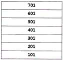
101:基底101: Substrate
201:阳极201: Anode
301:空穴注入层301: hole injection layer
401:空穴传输层401: hole transport layer
501:发光层501: Light Emitting Layer
601:电子传输层601: Electron Transport Layer
701:阴极701: Cathode
具体实施方式Detailed ways
下文中,将对本说明书进行详细地描述。Hereinafter, the present specification will be described in detail.
在本说明书中,当一个构件设置在另一构件“上”时,这不仅包括一个构件与另一构件接触的情况,而且还包括在这两个构件之间存在又一构件的情况。In this specification, when a member is disposed "on" another member, it includes not only the case where the one member is in contact with the other member, but also the case where there is another member between the two members.
在本说明书中,除非另有具体描述,否则当一部分“包括”一个构成要素时,这不意指排除另外的构成要素,而是意指还可以包括另外的构成要素。In this specification, unless specifically described otherwise, when a part "includes" one constituent element, it does not mean that the other constituent element is excluded, but it means that the other constituent element may also be included.
本说明书的一个示例性实施方案提供了用于有机电致发光器件的空穴注入或传输层或者电荷产生层的涂覆组合物,该涂覆组合物包含:包含第V族、第VI族和第VII族过渡金属中的一者或更多者的有机金属配合物;包含第I族、第VIII族、第XI族和第XII族金属中的一者或更多者的有机金属配合物或金属盐;以及有机溶剂。An exemplary embodiment of the present specification provides a coating composition for a hole injection or transport layer or a charge generation layer of an organic electroluminescent device, the coating composition comprising: comprising Group V, Group VI and Organometallic complexes of one or more of Group VII transition metals; organometallic complexes comprising one or more of Group I, Group VIII, Group XI and Group XII metals or metal salts; and organic solvents.
由于第V族、第VI族或第VII族过渡金属和第I族、第VIII族、第XI族和第XII族金属的金属氧化物的氧化数不同,并且这些氧化物具有不同的功函数,因此通过掺杂或混合这些氧化物最终产生的薄膜的功函数不同。因此,可以通过调节待掺杂或混合的金属的类型和量使功函数多样化。因此,可以通过根据空穴传输层、发光层和设置在上层上的电子传输层的类型或特性匹配功函数来调节器件中空穴与电子之间的平衡,从而实现长使用寿命并调节发光效率。Since the oxidation numbers of the metal oxides of the Group V, VI or VII transition metals and the Group I, VIII, XI and XII metals are different, and these oxides have different work functions, Thus the final films produced by doping or mixing these oxides have different work functions. Therefore, the work function can be diversified by adjusting the type and amount of metals to be doped or mixed. Therefore, the balance between holes and electrons in the device can be adjusted by matching the work function according to the types or characteristics of the hole transport layer, the light emitting layer, and the electron transport layer disposed on the upper layer, thereby achieving a long lifetime and adjusting the luminous efficiency.
包含第V族、第VI族或第VII族过渡金属中的一者或更多者的有机金属配合物可以优选地包含Mo、W、V或Re,并且更优选Mo。The organometallic complex comprising one or more of a Group V, Group VI or Group VII transition metal may preferably comprise Mo, W, V or Re, and more preferably Mo.
包含第I族、第VIII族、第XI族和第XII族金属中的一者或更多者的有机金属配合物或金属盐可以包含:碱金属,例如Li、Na、K、Rb和Cs;过渡金属,例如Fe、Ru、Os、Cu、Ag、Au、Zn和Cd;等等。The organometallic complex or metal salt comprising one or more of Group I, Group VIII, Group XI and Group XII metals may comprise: alkali metals such as Li, Na, K, Rb and Cs; Transition metals such as Fe, Ru, Os, Cu, Ag, Au, Zn, and Cd; and the like.
包含第I族、第VIII族、第XI族和第XII族金属中的一者或更多者的有机金属配合物或金属盐更优选地包含第I族的碱金属例如Li、Na、K、Rb或Cs,并且可以更优选地包含Na。Organometallic complexes or metal salts comprising one or more of Group I, Group VIII, Group XI and Group XII metals more preferably comprise Group I alkali metals such as Li, Na, K, Rb or Cs, and may more preferably contain Na.
根据一个实例,涂覆组合物可以包含含有Mo、W、V或Re的有机金属配合物和含有Li、Na、K、Rb或Cs的有机金属配合物或金属盐。According to one example, the coating composition may comprise an organometallic complex containing Mo, W, V or Re and an organometallic complex or metal salt containing Li, Na, K, Rb or Cs.
根据一个实例,涂覆组合物可以包含含有Mo、W、V或Re的有机金属配合物和含有Fe、Ru、Cu、Ag、Au或Zn的有机金属配合物或金属盐。According to one example, the coating composition may comprise an organometallic complex containing Mo, W, V or Re and an organometallic complex or metal salt containing Fe, Ru, Cu, Ag, Au or Zn.
如果可能的话,优选的是包含Mo、W、V或Re的有机金属配合物具有足够的有机材料部分以具有良好的溶解性和良好的可涂覆性,但是由于优选的是有机金属配合物的配体在热处理期间被除去,使得有机金属配合物变成金属氧化物,因此优选具有在350℃或更低时热分解的配体。此外,与有机金属配合物混合的金属元素的前体可以具有配体,例如各种元素的有机配合物,如甲醇酯/盐、乙醇酯/盐、异丙醇酯/盐、丁醇酯/盐、乙酸酯/盐和乙酰丙酮化物,并且前体也可以是卤化物、硝酸酯/盐和硫酸酯/盐。然而,优选的是,在热处理之后不残留这些有机配体和盐的阴离子部分。If possible, it is preferred that the organometallic complexes containing Mo, W, V or Re have sufficient organic material moieties to have good solubility and good coatability, but since it is preferred that the organometallic complexes have The ligand is removed during the heat treatment, so that the organometallic complex becomes a metal oxide, so it is preferable to have a ligand that is thermally decomposed at 350°C or lower. In addition, precursors of metal elements mixed with organometallic complexes may have ligands, such as organic complexes of various elements, such as methanol ester/salt, ethanol ester/salt, isopropanol ester/salt, butanol ester/salt Salts, acetates and acetylacetonates, and precursors may also be halides, nitrates and sulfates. Preferably, however, no anionic moieties of these organic ligands and salts remain after heat treatment.
根据一个实例,涂覆组合物可以包含含有Mo、W、V或Re的有机金属配合物和含有Cu的有机金属配合物或金属盐。According to one example, the coating composition may comprise an organometallic complex containing Mo, W, V or Re and an organometallic complex or metal salt containing Cu.
根据另一个实例,涂覆组合物可以包含含有Mo、W、V或Re的有机金属配合物和含有Na的有机金属配合物或金属盐。According to another example, the coating composition may comprise an organometallic complex containing Mo, W, V or Re and an organometallic complex or metal salt containing Na.
根据又一个实例,涂覆组合物可以包含含有Mo、W、V或Re的有机金属配合物和含有Ag的有机金属配合物或金属盐。According to yet another example, the coating composition may comprise an organometallic complex containing Mo, W, V or Re and an organometallic complex or metal salt containing Ag.
根据又一个实例,涂覆组合物可以包含含有Mo、W、V或Re的有机金属配合物和含有Fe的有机金属配合物或金属盐。According to yet another example, the coating composition may comprise an organometallic complex containing Mo, W, V or Re and an organometallic complex or metal salt containing Fe.
根据又一个实例,涂覆组合物可以包含含有Mo、W、V或Re的有机金属配合物和含有Cs的有机金属配合物或金属盐。According to yet another example, the coating composition may comprise an organometallic complex containing Mo, W, V or Re and an organometallic complex or metal salt containing Cs.
根据又一个实例,涂覆组合物可以包含含有Mo、W、V或Re的有机金属配合物和含有Zn的有机金属配合物或金属盐。According to yet another example, the coating composition may comprise an organometallic complex containing Mo, W, V or Re and an organometallic complex or metal salt containing Zn.
根据又一个实例,涂覆组合物可以包含含有Mo、W、V或Re的有机金属配合物和含有Au的有机金属配合物或金属盐。According to yet another example, the coating composition may comprise an organometallic complex containing Mo, W, V or Re and an organometallic complex or metal salt containing Au.
根据又一个实例,涂覆组合物可以包含含有Mo、W、V或Re的有机金属配合物和含有K的有机金属配合物或金属盐。According to yet another example, the coating composition may comprise an organometallic complex containing Mo, W, V or Re and an organometallic complex or metal salt containing K.
根据又一个实例,涂覆组合物可以包含含有Mo、W、V或Re的有机金属配合物和含有Rb的有机金属配合物或金属盐。According to yet another example, the coating composition may comprise an organometallic complex containing Mo, W, V or Re and an organometallic complex or metal salt containing Rb.
根据又一个实例,涂覆组合物可以包含含有Mo、W、V或Re的有机金属配合物和含有Ru的有机金属配合物或金属盐。According to yet another example, the coating composition may comprise an organometallic complex containing Mo, W, V or Re and an organometallic complex or metal salt containing Ru.
根据另一个示例性实施方案,涂覆组合物中第V族、第VI族或第VII族有机金属配合物的含量比率为0.01重量%至50重量%,并且与第V族、第VI族或第VII族过渡金属原子混合的第I族、第VIII族、第XI族和第XII族金属元素的比率为0.01原子%至50原子%。基于总金属原子,涂覆组合物中的第V族、第VI族或第VII族金属可以以50原子%至99.99原子%的量存在。According to another exemplary embodiment, the content ratio of the Group V, Group VI or Group VII organometallic complex in the coating composition is 0.01 wt % to 50 wt %, and the content ratio of the Group V, Group VI or The ratio of the Group I, Group VIII, Group XI and Group XII metal elements in which the Group VII transition metal atoms are mixed is 0.01 atomic % to 50 atomic %. The Group V, Group VI, or Group VII metal in the coating composition may be present in an amount from 50 atomic percent to 99.99 atomic percent based on total metal atoms.
在示例性实施方案中,有机金属配合物和金属盐可以是氧化数为-2至+6的配合物。有机金属配合物包含与金属键合的上述有机配体。有机配体没有特别限制,但是可以考虑溶剂溶解性或与相邻有机材料层的界面特性等来选择。有机配体的实例包括羰基、乙酰基、乙酰丙酮基、乙酰乙酸甲酯基、乙酰乙酸乙酯基、硫代乙酸酯/盐、异氰酸酯/盐、氰酸酯/盐、异氰酸酯/盐、硝酸酯/盐、己酸酯/盐、柠檬酸酯/盐、卤素原子等。此外,有机配体可以具有包含芳族环和/或杂环的结构,并且可以是例如:苯、三苯胺、芴、联苯、芘、蒽、咔唑、苯基吡啶、三噻吩、苯基
有机配体的具体实例包括基于烷氧基的配体或基于乙酸酯/盐的配体,例如乙酰丙酮化物(acac)、乙酰乙酸乙酯、乙酰乙酸甲酯、OPh、羰基、甲氧基、乙氧基、丙氧基、异丙氧基、丁氧基、仲丁氧基、叔丁氧基、戊氧基、己氧基、庚氧基、辛氧基和乙基己氧基,但不限于此。此外,有机配体可以是有机配体和卤素基团共存形式的配体。Specific examples of organic ligands include alkoxy-based ligands or acetate/salt-based ligands such as acetylacetonate (acac), ethyl acetoacetate, methyl acetoacetate, OPh, carbonyl, methoxy , ethoxy, propoxy, isopropoxy, butoxy, sec-butoxy, tert-butoxy, pentyloxy, hexyloxy, heptyloxy, octyloxy and ethylhexyloxy, But not limited to this. In addition, the organic ligand may be a ligand in the form of coexistence of an organic ligand and a halogen group.
有机金属配合物可以包含金属氧化物。金属氧化物可以包括包含第V族、第VI族或第VII族过渡金属中的一者或更多者或者包含第I族、第VIII族、第XI族和第XII族金属中的一者或更多者的金属氧化物,并且上述有机配体可以与该金属氧化物配位。有机金属配合物的实例包括:W(CO)6、W(acac)3、Mo(CO)6、WO2Cl2、MoO2(acac)2、硝酸钠、Zn(acac)2、乙酸铁和硝酸铯。作为另一个实例,当有机金属配合物包含V时,有机金属配合物可以是其中一部分被氧取代的VO(acac)2,并且可以是其中未被氧取代的V(acac)3。作为又一个实例,甚至当有机金属配合物包含W时,有机金属配合物也可以是W(acac)3,并且还可以是被部分氧化的WO(acac)2。The organometallic complex may contain metal oxides. The metal oxide may comprise one or more of a transition metal of Group V, Group VI, or Group VII or one of a metal of Group I, Group VIII, Group XI, and Group XII, or More metal oxides, and the above-mentioned organic ligands may coordinate with the metal oxides. Examples of organometallic complexes include: W(CO)6 , W(acac)3 , Mo(CO)6 ,WO2Cl2 , MoO2(acac)2, sodium nitrate, Zn(acac)2, iron acetate and Cesium nitrate. As another example, when the organometallic complex includes V, the organometallic complex may be VO(acac)2 in which a portion is substituted with oxygen, and may be V(acac)3 in which it is not substituted with oxygen. As yet another example, even when the organometallic complex contains W, the organometallic complex may be W(acac)3 , and may also be partially oxidized WO(acac)2 .
此外,有机金属配合物可以是两种或更多种不同配体彼此键合的形式。例如,有机金属配合物可以是二氯二氧化钼。Furthermore, the organometallic complex may be in the form of two or more different ligands bonded to each other. For example, the organometallic complex can be molybdenum dioxide dichloride.
在一个示例性实施方案中,有机溶剂可以包含羟基和酮基中的至少一者。In an exemplary embodiment, the organic solvent may contain at least one of a hydroxyl group and a ketone group.
在一个示例性实施方案中,有机溶剂是基于醇的溶剂。In an exemplary embodiment, the organic solvent is an alcohol-based solvent.
在另一个示例性实施方案中,有机溶剂是基于酮的溶剂。In another exemplary embodiment, the organic solvent is a ketone-based solvent.
在本说明书中,具有羟基或酮基的有机溶剂的实例可以包括丙酮、甲基乙基酮、二乙基酮、环己酮、环戊酮、异佛尔酮、乙酰丙酮、四氢萘酮、苯甲酸乙酯、苯甲酸甲酯、苯甲酸丁酯、乙酸乙酯、乙酰乙酸乙酯、乙酰乙酸二乙酯、苯甲酸甲酯、苯甲酸乙酯、甲醇、乙醇、丙醇、异丙醇、丁醇、仲丁醇、叔丁醇、戊醇、环戊醇、己醇、环己醇、庚醇和辛醇,并且可以是由以下通式1表示的溶剂。In the present specification, examples of the organic solvent having a hydroxyl or ketone group may include acetone, methyl ethyl ketone, diethyl ketone, cyclohexanone, cyclopentanone, isophorone, acetylacetone, tetralone , ethyl benzoate, methyl benzoate, butyl benzoate, ethyl acetate, ethyl acetoacetate, diethyl acetoacetate, methyl benzoate, ethyl benzoate, methanol, ethanol, propanol, isopropyl Alcohol, butanol, sec-butanol, tert-butanol, pentanol, cyclopentanol, hexanol, cyclohexanol, heptanol, and octanol, and may be a solvent represented by the following general formula 1.
通式1Formula 1

在通式1中,n为1至20的整数,l和m各自为或者均为0至5的整数,并且R1、R2、R3和R4各自为或者全部为氢原子、具有1至20个碳原子的烷基、具有2至20个碳原子的烯基、具有2至20个碳原子的炔基、具有1至20个碳原子的烷氧基、具有6至40个碳原子的芳基、具有2至40个碳原子的杂芳基、或者具有1至20个碳原子的酯基。In Formula 1, n is an integer of 1 to 20, l and m are each or both an integer of 0 to 5, and R1 , R2 , R3 and R4 are each or all of a hydrogen atom, having 1 Alkyl of to 20 carbon atoms, alkenyl of 2 to 20 carbon atoms, alkynyl of 2 to 20 carbon atoms, alkoxy of 1 to 20 carbon atoms, 6 to 40 carbon atoms aryl group, heteroaryl group having 2 to 40 carbon atoms, or ester group having 1 to 20 carbon atoms.
根据一个示例性实施方案,有机溶剂的沸点优选为350℃或更低。作为具体实例,可以使用乙二醇、乙二醇单甲醚、乙二醇单乙醚、乙二醇单丙醚、乙二醇单丁醚、乙二醇单戊醚、乙二醇单己醚、乙二醇二甲醚、乙二醇二乙醚、乙二醇二丙醚、乙二醇二丁醚、乙二醇二戊醚、乙二醇二己醚、1,2-丙二醇、1,3-丙二醇、1,4-丁二醇、1,2-丁二醇、1,3-丁二醇、二乙二醇、二乙二醇单甲醚、二乙二醇单乙醚、二乙二醇单丙醚、二乙二醇单丁醚、二亚乙基二甲醚、二乙二醇二乙醚、二乙二醇二丙醚、二乙二醇二丁醚、乙二醇二乙酸酯、PEG 600、三甘醇等。According to an exemplary embodiment, the boiling point of the organic solvent is preferably 350°C or lower. As specific examples, ethylene glycol, ethylene glycol monomethyl ether, ethylene glycol monoethyl ether, ethylene glycol monopropyl ether, ethylene glycol monobutyl ether, ethylene glycol monoamyl ether, ethylene glycol monohexyl ether can be used , ethylene glycol dimethyl ether, ethylene glycol diethyl ether, ethylene glycol dipropyl ether, ethylene glycol dibutyl ether, ethylene glycol dipentyl ether, ethylene glycol dihexyl ether, 1,2-propylene glycol, 1, 3-Propanediol, 1,4-Butanediol, 1,2-Butanediol, 1,3-Butanediol, Diethylene glycol, Diethylene glycol monomethyl ether, Diethylene glycol monoethyl ether, Diethyl ether Glycol monopropyl ether, diethylene glycol monobutyl ether, diethylene dimethyl ether, diethylene glycol diethyl ether, diethylene glycol dipropyl ether, diethylene glycol dibutyl ether, ethylene glycol diethyl ether acid ester, PEG 600, triethylene glycol, etc.
由通式1表示的溶剂的优点在于,可以在不与上述特别是用作金属氧化物的前体的有机金属配合物形成化学强键的情况下,通过使金属氧化物的前体不容易变成另一种氧化态或物质来制成在制造器件之后不留下有机材料的氧化物薄膜。The advantage of the solvent represented by the general formula 1 is that it is possible to make the precursor of the metal oxide less easily changeable without forming a strong chemical bond with the above-mentioned organometallic complex in particular, which is used as the precursor of the metal oxide. to another oxidation state or species to make an oxide film that leaves no organic material behind after the device is fabricated.
根据一个示例性实施方案,优选的是,涂覆组合物中包含第V族、第VI族或第VII族过渡金属中的一者或更多者的有机金属配合物的含量为0.01重量%至50重量%。根据一个示例性实施方案,基于第V族、第VI族或第VII族过渡金属,涂覆组合物中包含第I族、第VIII族、第XI族和第XII族金属中的一者或更多者的有机金属配合物或金属盐的含量可以为0.01重量%至50重量%,优选1重量%至20重量%,并且更优选1重量%至15重量%。当包含第I族、第VIII族、第XI族和第XII族金属中的一者或更多者的有机金属配合物或金属盐相对于第V族、第VI族或第VII族过渡金属满足该含量范围时,存在器件的使用寿命特性优异的益处。According to an exemplary embodiment, it is preferred that the content of the organometallic complex comprising one or more of the transition metals of Group V, Group VI or Group VII in the coating composition is 0.01 wt % to 50% by weight. According to an exemplary embodiment, one or more of a Group I, Group VIII, Group XI, and Group XII metal is included in the coating composition based on a Group V, Group VI, or Group VII transition metal. The organometallic complex or metal salt of multiple may be present in an amount of 0.01 to 50% by weight, preferably 1 to 20% by weight, and more preferably 1 to 15% by weight. When an organometallic complex or metal salt comprising one or more of a Group I, Group VIII, Group XI and Group XII metal satisfies with respect to a Group V, Group VI or Group VII transition metal Within this content range, there is an advantage that the service life characteristics of the device are excellent.
除了有机金属配合物之外,涂覆组合物还可以包含添加剂以改善特性例如可涂覆性和粘度。例如,添加剂可以包括选自以下的任一者或更多者:分散剂、表面活性剂、聚合物、粘合剂、交联剂、乳化剂、消泡剂、干燥剂、填料、填充剂、增稠剂、膜调节剂、抗氧化剂、流化剂、平整度添加剂和腐蚀抑制剂。In addition to the organometallic complex, the coating composition may also contain additives to improve properties such as coatability and viscosity. For example, additives may include any one or more selected from the group consisting of dispersants, surfactants, polymers, binders, crosslinking agents, emulsifiers, defoamers, desiccants, fillers, fillers, Thickeners, Film Conditioners, Antioxidants, Fluidizers, Flatness Additives and Corrosion Inhibitors.
本说明书的另一个示例性实施方案涉及用于制造有机电致发光器件的方法,该方法包括:Another exemplary embodiment of the present specification relates to a method for fabricating an organic electroluminescent device, the method comprising:
准备基底;prepare the substrate;
在基底上形成第一电极;forming a first electrode on the substrate;
在第一电极上形成具有一个或更多个层的有机材料层;以及forming an organic material layer having one or more layers on the first electrode; and
在有机材料层上形成第二电极,forming a second electrode on the organic material layer,
其中该方法还包括通过使用根据示例性实施方案的上述涂覆组合物的涂覆法在第一电极与有机材料层之间、第二电极与有机材料层之间、或者当存在两个或更多个有机材料层时在有机材料层之间形成空穴注入或传输层或者电荷产生层。Wherein the method further includes between the first electrode and the organic material layer, between the second electrode and the organic material layer, or when there are two or more, by a coating method using the above coating composition according to the exemplary embodiment In the case of a plurality of organic material layers, a hole injection or transport layer or a charge generation layer is formed between the organic material layers.
用于形成空穴注入或传输层或者电荷产生层的涂覆方法可以是例如选自以下的任一种:旋涂体系、喷墨体系、喷嘴印刷、湿涂、喷涂、刮刀涂覆、接触印刷、顶部进料反向印刷、底部进料反向印刷、喷嘴进料反向印刷、凹版印刷、微凹版印刷、反向微凹版印刷、辊涂、狭缝模涂覆、毛细管涂覆、喷射沉积和喷雾沉积,并且可以优选为旋涂、喷墨涂覆、喷嘴印刷等。The coating method for forming the hole injection or transport layer or the charge generation layer may be, for example, any one selected from the group consisting of spin coating systems, ink jet systems, nozzle printing, wet coating, spray coating, blade coating, contact printing , Top Feed Reverse Printing, Bottom Feed Reverse Printing, Nozzle Feed Reverse Printing, Gravure Printing, Micro Gravure Printing, Reverse Micro Gravure Printing, Roll Coating, Slot Die Coating, Capillary Coating, Jet Deposition and spray deposition, and may preferably be spin coating, ink jet coating, nozzle printing, and the like.
涂覆方法可以通过将上述组合物涂覆至第一电极或第二电极上,然后干燥该组合物来进行。干燥或热处理或者干燥之后的热处理可以在氮气中或空气中进行,但是在空气中的干燥或热处理或者干燥之后的热处理有利于除去溶剂和有机材料配体并且有利于将有机金属配合物转化为氧化物。此外,热处理的处理温度可以根据所使用的有机金属配合物而变化,但优选的是,在150℃或更高且300℃或更低、优选在200℃或更高且300℃或更低下进行热处理。The coating method may be performed by coating the above-described composition on the first electrode or the second electrode, and then drying the composition. Drying or heat treatment or heat treatment after drying can be carried out in nitrogen or in air, but drying or heat treatment in air or heat treatment after drying facilitates removal of solvents and organic material ligands and facilitates conversion of organometallic complexes to oxides thing. Furthermore, the treatment temperature of the heat treatment may vary depending on the organometallic complex used, but is preferably performed at 150°C or higher and 300°C or lower, preferably 200°C or higher and 300°C or lower heat treatment.
在本说明书中,当涂覆组合物包含含有第V族、第VI族或第VII族过渡金属中的一者或更多者的有机金属配合物和含有第I族、第VIII族、第XI族和第XII族金属中的一者或更多者的有机金属配合物或金属盐,并且空穴注入或传输层或者电荷产生层的热处理温度在该温度范围内时,可以在整个温度范围内制造具有优异的使用寿命特性的器件。In this specification, when the coating composition comprises an organometallic complex containing one or more of a transition metal of Group V, Group VI or Group VII and a Organometallic complexes or metal salts of one or more of Group and XII metals, and when the heat treatment temperature of the hole injection or transport layer or the charge generation layer is within this temperature range, may be over the entire temperature range Manufacture of devices with excellent lifetime characteristics.
然而,当涂覆组合物包含:包含第V族、第VI族或第VII族过渡金属中的一者或更多者的有机金属配合物;并且包含属于第I族、第VIII族、第XI族和第XII族之外的族的金属元素(特别是对应于第IV族的Ti元素)的有机金属配合物或金属盐时,难以制造具有优异的使用寿命特性的器件,并且由于器件的使用寿命特性仅在特定温度下增强,因此无法在整个过程温度内制造具有优异的使用寿命特性的器件。However, when the coating composition comprises: an organometallic complex comprising one or more of a transition metal of Group V, Group VI, or Group VII; In the case of organometallic complexes or metal salts of metal elements of Groups and Groups other than Group XII (particularly corresponding to Ti elements of Group IV), it is difficult to manufacture devices with excellent lifetime characteristics, and due to the use of Lifetime characteristics are enhanced only at specific temperatures, so it is not possible to manufacture devices with excellent lifetime characteristics over the entire process temperature.
根据一个示例性实施方案,通过使用涂覆组合物形成的空穴注入或传输层或者电荷产生层的厚度为1nm至1000nm。通常,在有机电致发光器件中,由于腔效应,需要对器件的总厚度进行优化,并且在厚度优化期间,其厚度需要根据上层的材料从几nm变化至1微米。此时,当电荷注入或传输层的厚度可以多样化而器件特性没有任何劣化时,对上层的器件结构和厚度变化的限制减少,这有利于提供优化的器件特性。本发明中提供的空穴注入或传输层提供了电压不会随着厚度增加的材料和器件。According to an exemplary embodiment, the hole injection or transport layer or the charge generation layer formed by using the coating composition has a thickness of 1 nm to 1000 nm. Generally, in organic electroluminescent devices, due to cavity effects, the overall thickness of the device needs to be optimized, and during thickness optimization, its thickness needs to vary from a few nm to 1 micrometer depending on the material of the upper layer. At this time, when the thickness of the charge injection or transport layer can be diversified without any degradation of device characteristics, restrictions on the device structure and thickness variation of the upper layer are reduced, which is beneficial to provide optimized device characteristics. The hole injection or transport layers provided in the present invention provide materials and devices where the voltage does not increase with thickness.
根据另一个示例性实施方案,制造方法还包括形成通过使用涂覆组合物形成的空穴注入或传输层或者电荷产生层,然后对该层进行退火。退火可以在150℃至250℃,优选在180℃至250℃下进行。由于本发明中的退火旨在除去有机金属配合物的有机配体并使有机金属配合物在退火过程期间变成金属氧化物,因此优选的是,温度足够高以使有机金属配合物的配体被分解,并且优选的是,在含氧气氛下进行退火以使配体变为氧化物。According to another exemplary embodiment, the manufacturing method further includes forming a hole injection or transport layer or a charge generation layer formed by using the coating composition, and then annealing the layer. Annealing can be performed at 150°C to 250°C, preferably 180°C to 250°C. Since the annealing in the present invention aims to remove the organic ligands of the organometallic complex and turn the organometallic complex into a metal oxide during the annealing process, it is preferred that the temperature is high enough to cause the ligands of the organometallic complex to is decomposed and, preferably, annealed in an oxygen-containing atmosphere to convert the ligands to oxides.
在一个示例性实施方案中,除了空穴注入或传输层或者电荷产生层通过使用根据示例性实施方案的上述涂覆组合物来形成之外,可以使用本领域已知的那些用于其他电极和有机材料层的材料和制造方法。In an exemplary embodiment, in addition to the hole injection or transport layer or the charge generation layer formed by using the above-described coating composition according to the exemplary embodiment, those known in the art may be used for other electrodes and Materials and manufacturing methods of organic material layers.
根据一个实例,第一电极是阳极,并且第二电极是阴极。According to one example, the first electrode is an anode and the second electrode is a cathode.
根据另一个实例,第二电极是阳极,并且第一电极是阴极。According to another example, the second electrode is an anode and the first electrode is a cathode.
根据一个实例,有机材料层包括发光层。According to one example, the organic material layer includes a light-emitting layer.
根据另一个实例,有机材料层可以由多层结构构成,并且例如包括以下的至少一个层:发光层、空穴注入层、空穴传输层、电子传输层、电子注入层、电子阻挡层和空穴阻挡层。例如,根据本说明书的一个示例性实施方案的有机电致发光器件的结构例示在图1中。According to another example, the organic material layer may be composed of a multi-layer structure and, for example, include at least one of the following layers: a light emitting layer, a hole injection layer, a hole transport layer, an electron transport layer, an electron injection layer, an electron blocking layer, and a void hole barrier. For example, the structure of an organic electroluminescence device according to an exemplary embodiment of the present specification is illustrated in FIG. 1 .
图1例示出有机电致发光器件的结构,其中在基底101上依次堆叠有阳极201、空穴注入层301、空穴传输层401、发光层501、电子传输层601和阴极701。在图1中,空穴注入层301可以通过使用上述涂覆组合物而形成。然而,图1例示出有机电致发光器件,并且有机电致发光器件的结构不限于此。1 illustrates the structure of an organic electroluminescent device, in which an
当有机电致发光器件包括复数个有机材料层时,有机材料层可以由相同材料或不同材料形成。When the organic electroluminescent device includes a plurality of organic material layers, the organic material layers may be formed of the same material or different materials.
例如,本说明书的有机电致发光器件可以通过将阳极、有机材料层和阴极依次堆叠在基底上来制造。此时,有机电致发光器件可以如下进行制造:通过使用物理气相沉积(PVD)法(例如溅射或电子束蒸镀)使金属或具有导电性的金属氧化物或其合金沉积在基底上以形成阳极,在阳极上形成包括空穴注入层、空穴传输层、发光层和电子传输层的有机材料层,然后在有机材料层上沉积可以用作阴极的材料。除了上述方法之外,有机电致发光器件还可以通过使阴极材料、有机材料层和阳极材料依次沉积在基底上来制造。此时,可以通过使用溶液法形成设置在阳极与阴极之间的至少一个层或所有的层。溶液法的实例包括印刷方法,例如喷墨印刷、喷嘴印刷、胶版印刷、转印或丝网印刷等,但不限于此。当使用溶液法时,在器件制造期间在时间和成本方面存在经济效应。当有机材料层经受溶液法时,如果需要,可以另外进行热处理或光处理。此处,可以根据过程条件或使用的材料来选择热处理的温度和时间,并且热处理可以在例如85℃至300℃下进行1分钟至1小时。For example, the organic electroluminescent device of the present specification can be fabricated by sequentially stacking an anode, an organic material layer, and a cathode on a substrate. At this time, the organic electroluminescent device can be manufactured by depositing a metal or a conductive metal oxide or an alloy thereof on a substrate by using a physical vapor deposition (PVD) method such as sputtering or electron beam evaporation to An anode is formed, an organic material layer including a hole injection layer, a hole transport layer, a light emitting layer and an electron transport layer is formed on the anode, and then a material that can be used as a cathode is deposited on the organic material layer. In addition to the above methods, organic electroluminescent devices can also be fabricated by sequentially depositing a cathode material, an organic material layer, and an anode material on a substrate. At this time, at least one layer or all of the layers disposed between the anode and the cathode may be formed by using a solution method. Examples of the solution method include printing methods such as ink jet printing, nozzle printing, offset printing, transfer printing or screen printing, etc., but are not limited thereto. When solution methods are used, there are economic effects in terms of time and cost during device fabrication. When the organic material layer is subjected to the solution method, if necessary, heat treatment or light treatment may be additionally performed. Here, the temperature and time of the heat treatment may be selected according to process conditions or materials used, and the heat treatment may be performed at, for example, 85° C. to 300° C. for 1 minute to 1 hour.
作为阳极材料,通常优选具有高的功函数的材料以促进空穴注入有机材料层。可以用于本发明的阳极材料的具体实例包括:金属,例如钒、铬、铜、锌和金,或其合金;金属氧化物,例如氧化锌、氧化铟、氧化铟锡(ITO)、氧化铟锌(IGZO)、氟掺杂的氧化锡(FTO)和氧化铟锌(IZO);金属和氧化物的组合,例如ZnO:Al或SnO2:Sb;导电聚合物,例如聚(3-甲基噻吩)、聚[3,4-(亚乙基-1,2-二氧基)噻吩](PEDOT)、聚吡咯和聚苯胺;等等,但不限于此。As the anode material, a material having a high work function is generally preferred to facilitate hole injection into the organic material layer. Specific examples of anode materials that can be used in the present invention include: metals such as vanadium, chromium, copper, zinc and gold, or alloys thereof; metal oxides such as zinc oxide, indium oxide, indium tin oxide (ITO), indium oxide Zinc (IGZO), fluorine-doped tin oxide (FTO), and indium zinc oxide (IZO); combinations of metals and oxides, such as ZnO:Al orSnO2 :Sb; conducting polymers, such as poly(3-methyl) thiophene), poly[3,4-(ethylene-1,2-dioxy)thiophene] (PEDOT), polypyrrole, and polyaniline; and the like, but not limited thereto.
作为阴极材料,通常优选具有低的功函数的材料以促进电子注入有机材料层。阴极材料的具体实例包括:金属,例如镁、钙、钠、钾、钛、铟、钇、锂、钆、铝、银、锡和铅,或其合金;多层结构材料,例如LiF/Al或LiO2/Al;等等,但不限于此。As a cathode material, a material having a low work function is generally preferred to facilitate electron injection into the organic material layer. Specific examples of cathode materials include: metals such as magnesium, calcium, sodium, potassium, titanium, indium, yttrium, lithium, gadolinium, aluminum, silver, tin, and lead, or alloys thereof; multilayered structural materials such as LiF/Al or LiO2 /Al; etc., but not limited thereto.
在形成通过使用包含有机金属配合物的上述涂覆组合物形成的空穴注入或传输层之外的另外的空穴注入层时,用于空穴注入层的材料优选为这样的化合物:其具有传输空穴的能力并因此在阳极处具有空穴注入效应,对发光层或发光材料具有优异的空穴注入效应,防止由发光层产生的激子移动至电子注入层或电子注入材料,并且形成薄膜的能力也优异。空穴注入材料的最高占据分子轨道(HOMO)优选为介于阳极材料的功函数与周围有机材料层的HOMO之间的值。空穴注入材料的具体实例包括金属卟啉、低聚噻吩、基于芳基胺的有机材料、基于六腈六氮杂苯并菲的有机材料、基于喹吖啶酮的有机材料、基于苝的有机材料、蒽醌、基于聚苯胺和基于聚噻吩的导电聚合物等,但不限于此。When forming an additional hole injection layer other than the hole injection or transport layer formed by using the above-mentioned coating composition containing an organometallic complex, the material for the hole injection layer is preferably a compound having The ability to transport holes and thus have a hole injection effect at the anode, have an excellent hole injection effect on the light-emitting layer or light-emitting material, prevent excitons generated by the light-emitting layer from moving to the electron injection layer or electron injection material, and form The ability of thin films is also excellent. The highest occupied molecular orbital (HOMO) of the hole injection material is preferably a value between the work function of the anode material and the HOMO of the surrounding organic material layer. Specific examples of hole injection materials include metalloporphyrins, oligothiophenes, arylamine-based organic materials, hexanitrile hexaazatriphenylene-based organic materials, quinacridone-based organic materials, perylene-based organic materials. materials, anthraquinone, polyaniline-based and polythiophene-based conductive polymers, etc., but not limited thereto.
空穴传输层是接收来自空穴注入层的空穴并将空穴传输至发光层的层,并且空穴传输材料适当地为具有高的空穴迁移率的材料,其可接收来自阳极或空穴注入层的空穴并将空穴传输至发光层。其具体实例包括基于芳基胺的有机材料、导电聚合物、具有共轭部分和非共轭部分二者的嵌段共聚物等,但不限于此。The hole transport layer is a layer that receives holes from the hole injection layer and transports the holes to the light emitting layer, and the hole transport material is suitably a material having high hole mobility, which can receive holes from the anode or the hole. The holes inject holes in the layer and transport the holes to the light emitting layer. Specific examples thereof include arylamine-based organic materials, conductive polymers, block copolymers having both a conjugated portion and a non-conjugated portion, and the like, but are not limited thereto.
发光材料是这样的材料:其可通过接收分别来自空穴传输层和电子传输层的空穴和电子并使其结合而发出可见光区域内的光,并且优选为对荧光或磷光具有良好量子效率的材料。其具体实例包括:8-羟基-喹啉铝配合物(Alq3);基于咔唑的化合物;二聚苯乙烯基化合物;BAlq;10-羟基苯并喹啉-金属化合物;基于苯并
发光层可以包含主体材料和掺杂剂材料。主体材料的实例包括稠合芳族环衍生物或含杂环的化合物等。具体地,稠合芳族环衍生物的实例包括蒽衍生物、芘衍生物、萘衍生物、并五苯衍生物、菲化合物、荧蒽化合物等,并且含杂环的化合物的实例包括咔唑衍生物、二苯并呋喃衍生物、梯子型呋喃化合物、嘧啶衍生物等,但其实例不限于此。The light emitting layer may contain a host material and a dopant material. Examples of the host material include fused aromatic ring derivatives or heterocyclic ring-containing compounds and the like. Specifically, examples of the fused aromatic ring derivatives include anthracene derivatives, pyrene derivatives, naphthalene derivatives, pentacene derivatives, phenanthrene compounds, fluoranthene compounds, and the like, and examples of the heterocycle-containing compound include carbazole Derivatives, dibenzofuran derivatives, ladder-type furan compounds, pyrimidine derivatives and the like, but examples thereof are not limited thereto.
掺杂剂材料的实例包括芳族胺衍生物、苯乙烯胺化合物、硼配合物、荧蒽化合物、金属配合物等。具体地,芳族胺衍生物为具有经取代或未经取代的芳基氨基的稠合芳族环衍生物,并且其实例包括具有芳基氨基的芘、蒽、
电子传输层是接收来自电子注入层的电子并将电子传输至发光层的层,并且电子传输材料适当地为可顺利地接收来阴极的电子并将电子传输至发光层的具有高电子迁移率的材料。其具体实例包括:8-羟基喹啉的Al配合物;包含Alq3的配合物;有机自由基化合物;羟基黄酮-金属配合物;等等,但不限于此。电子传输层可以与根据相关技术所使用的任何期望的阴极材料一起使用。特别地,阴极材料的适当实例为具有低功函数的典型材料,其后接铝层或银层。其具体实例包括铯、钡、钙、镱和钐,在每种情况下都后接铝层或银层。The electron transport layer is a layer that receives electrons from the electron injection layer and transports the electrons to the light emitting layer, and the electron transport material is suitably a material having high electron mobility that can smoothly receive electrons from the cathode and transport the electrons to the light emitting layer. Material. Specific examples thereof include: Al complexes of 8-hydroxyquinoline; complexes containing Alq3 ; organic radical compounds; hydroxyflavone-metal complexes; and the like, but are not limited thereto. The electron transport layer can be used with any desired cathode material used in accordance with the related art. In particular, suitable examples of cathode materials are typical materials with a low work function followed by a layer of aluminum or silver. Specific examples thereof include cesium, barium, calcium, ytterbium and samarium, in each case followed by a layer of aluminium or silver.
电子注入层是注入来自电极的电子的层,并且电子注入材料优选为这样的化合物:其具有传输电子的能力,具有从阴极注入电子的效应,并且具有将电子注入发光层或发光材料的优异效应,防止由发光层产生的激子移动至空穴注入层,并且形成薄膜的能力也优异。其具体实例包括芴酮、蒽醌二甲烷、联苯醌、噻喃二氧化物、

金属配合物化合物的实例包括8-羟基喹啉锂、双(8-羟基喹啉)锌、双(8-羟基喹啉)铜、双(8-羟基喹啉)锰、三(8-羟基喹啉)铝、三(2-甲基-8-羟基喹啉)铝、三(8-羟基喹啉)镓、双(10-羟基苯并[h]喹啉)铍、双(10-羟基苯并[h]喹啉)锌、双(2-甲基-8-喹啉)氯镓、双(2-甲基-8-喹啉)(邻甲酚)镓、双(2-甲基-8-喹啉)(1-萘酚)铝、双(2-甲基-8-喹啉)(2-萘酚)镓等,但不限于此。Examples of the metal complex compound include lithium 8-hydroxyquinoline, zinc bis(8-hydroxyquinoline), copper bis(8-hydroxyquinoline), manganese bis(8-hydroxyquinoline), tris(8-hydroxyquinoline) Lino) aluminum, tris(2-methyl-8-hydroxyquinoline) aluminum, tris(8-hydroxyquinoline) gallium, bis(10-hydroxybenzo[h]quinoline) beryllium, bis(10-hydroxybenzene) [h]quinoline)zinc, bis(2-methyl-8-quinoline)chlorogallium, bis(2-methyl-8-quinoline)(o-cresol)gallium, bis(2-methyl- 8-quinoline)(1-naphthol)aluminum, bis(2-methyl-8-quinoline)(2-naphthol)gallium, etc., but not limited thereto.
空穴阻挡层是阻挡空穴到达阴极的层,并且通常可以在与空穴注入层的条件相同的条件下形成。其具体实例包括
本说明书的又一个示例性实施方案提供了有机电致发光器件,其包括:Yet another exemplary embodiment of the present specification provides an organic electroluminescent device comprising:
第一电极;第二电极;和设置在第一电极与第二电极之间的具有一个或更多个层的有机材料层,a first electrode; a second electrode; and an organic material layer having one or more layers disposed between the first electrode and the second electrode,
其中有机电致发光器件还包括设置在第一电极与有机材料层之间、第二电极与有机材料层之间、或者当存在两个或更多个有机材料层时设置在有机材料层之间的空穴注入或传输层或者电荷产生层,并且Wherein the organic electroluminescence device further comprises being disposed between the first electrode and the organic material layer, between the second electrode and the organic material layer, or disposed between the organic material layers when there are two or more organic material layers a hole injection or transport layer or a charge generation layer, and
该空穴注入或传输层或者电荷产生层由包含第V族、第VI族和第VII族过渡金属中的一者或更多者以及第I族、第VIII族、第XI族和第XII族金属中的一者或更多者的金属氧化物构成。The hole injection or transport layer or charge generation layer is composed of a transition metal comprising one or more of Group V, Group VI, and Group VII and Group I, Group VIII, Group XI, and Group XII A metal oxide composition of one or more of the metals.
本说明书的又一个示例性实施方案提供了有机电致发光器件,其包括:第一电极;第二电极;和设置在第一电极与第二电极之间的具有一个或更多个层的有机材料层,其中该有机电致发光器件还包括空穴注入或传输层或者电荷产生层,该空穴注入或传输层或者电荷产生层设置在第一电极与有机材料层之间、第二电极与有机材料层之间、或者当存在两个或更多个有机材料层时设置在有机材料层之间,并且通过使用根据示例性实施方案的上述涂覆组合物而形成。Yet another exemplary embodiment of the present specification provides an organic electroluminescent device including: a first electrode; a second electrode; and an organic electroluminescent device having one or more layers disposed between the first electrode and the second electrode Material layer, wherein the organic electroluminescent device further comprises a hole injection or transport layer or a charge generation layer, the hole injection or transport layer or charge generation layer is arranged between the first electrode and the organic material layer, the second electrode and the The organic material layers are disposed between the organic material layers, or between the organic material layers when there are two or more organic material layers, and are formed by using the above-described coating composition according to the exemplary embodiment.
通过使用涂覆组合物形成的空穴注入或传输层或者电荷产生层由金属氧化物构成。此处,金属氧化物包含第V族、第VI族和第VII族过渡金属中的一者或更多者以及第I族、第VIII族、第XI族和第XII族金属中的一者或更多者。The hole injection or transport layer or the charge generation layer formed by using the coating composition is composed of a metal oxide. Here, the metal oxide comprises one or more of the transition metals of Group V, Group VI and Group VII and one of the metals of Group I, Group VIII, Group XI and Group XII or more.
根据另一个示例性实施方案,在空穴注入或传输层或者电荷产生层中的总金属原子中,第V族、第VI族或第VII族过渡金属的氧化物的含量比率为50原子%至99.99原子%。此外,基于100原子%的第V族、第VI族或第VII族过渡金属,与过渡金属混合的第I族、第VIII族、第XI族和第XII族金属原子的比率为0.01原子%至50原子%。根据一个实例,当将第V族、第VI族或第VII族过渡金属定义为M1,并且将待掺杂的金属元素定义为M2时,空穴注入或传输层或者电荷产生层可以由M1xM2yOz表示。此时,在0<x+y≤100的情况下,0<z≤400,50<x≤99.99并且0.01≤y<50。According to another exemplary embodiment, in the total metal atoms in the hole injection or transport layer or the charge generation layer, the content ratio of the oxide of the Group V, VI or Group VII transition metal is 50 atomic % to 99.99 atomic %. In addition, the ratio of Group I, Group VIII, Group XI and Group XII metal atoms mixed with the transition metal is 0.01 atomic % to 50 atomic %. According to an example, when the group V, VI or VII transition metal is defined as M1, and the metal element to be doped is defined as M2, the hole injection or transport layer or the charge generation layer may be represented by M1xM2yOz . At this time, in the case of 0<x+y≦100, 0<z≦400, 50<x≦99.99, and 0.01≦y<50.
根据另一个实例,空穴注入或传输层或者电荷产生层的功函数为5.0至7.0。According to another example, the work function of the hole injection or transport layer or the charge generation layer is 5.0 to 7.0.
根据一个实施,通过使用涂覆组合物形成的空穴注入或传输层或者电荷产生层的厚度为1nm至1000nm。此时,在空穴注入或传输层或者电荷产生层中,电荷浓度和迁移率由于在溶液法期间发生的掺杂效应而增加,因此,不会发生由厚度引起的电压降低。According to one implementation, the hole injection or transport layer or the charge generation layer formed by using the coating composition has a thickness of 1 nm to 1000 nm. At this time, in the hole injection or transport layer or the charge generation layer, the charge concentration and mobility are increased due to the doping effect that occurs during the solution method, and therefore, no reduction in voltage due to thickness occurs.
根据一个示例性实施方案,空穴注入或传输层或者电荷产生层包含M-O键和M-M键,并且此处,M为选自第I族、第V族至第VIII族、第XI族和第XII族的金属。According to an exemplary embodiment, the hole injection or transport layer or the charge generation layer includes M-O bonds and M-M bonds, and here, M is selected from Group I, Group V to Group VIII, Group XI, and Group XII family of metals.
根据一个示例性实施方案,空穴注入或传输层或者电荷产生层包含MO3和M2O5,并且此处,M为选自第I族、第V族至第VIII族、第XI族和第XII族的金属。例如,在MoO3的情况下,当通过溶液法出现Mo-Mo键时,MoO3的氧化数除了+6之外还有+5,并且作为借助于XPS对通过溶液法获得的薄膜进行分析的结果,可以确认检测到氧化数为+5(其为低氧化数)的Mo峰,如图2所示。此处,氧化数为+5的Mo的量没有特别限制,只要该量大于0即可。According to an exemplary embodiment, the hole injection or transport layer or the charge generation layer contains MO3 and M2 O5 , and here, M is selected from the group consisting of Group I, Group V to Group VIII, Group XI and Metals of Group XII. For example, in the case of MoO3, when the Mo- Mo bond occurs by the solution method, the oxidation numberof MoO3 is +5 in addition to +6, and as the analysis of the thin film obtained by the solution method by means of XPS As a result, it was confirmed that a Mo peak with an oxidation number of +5, which is a low oxidation number, was detected, as shown in FIG. 2 . Here, the amount of Mo having an oxidation number of +5 is not particularly limited as long as the amount is larger than 0.
根据另一个示例性实施例,空穴注入或传输层或者电荷产生层与第一电极或第二电极接触,并且与空穴注入或传输层或者电荷产生层和第一电极或第二电极接触的界面形成M-O-X键,并且此处,M为选自第I族、第V族至第VIII族、第XI族和第XII族的金属,X是构成与空穴注入或传输层或者电荷产生层接触的第一电极或第二电极的元素之一。例如,当如上所述在电极和空穴注入层薄膜之间形成M-O-X键时,可以改善粘合强度,并且可以增加空穴注入层自身的机械强度。According to another exemplary embodiment, the hole injection or transport layer or the charge generation layer is in contact with the first electrode or the second electrode, and the hole injection or transport layer or the charge generation layer is in contact with the first electrode or the second electrode The interface forms an M-O-X bond, and here, M is a metal selected from the group consisting of Group I, Group V to Group VIII, Group XI and Group XII, and X is a metal constituting contact with a hole injection or transport layer or a charge generation layer One of the elements of the first electrode or the second electrode. For example, when an M-O-X bond is formed between the electrode and the hole injection layer thin film as described above, the adhesive strength can be improved, and the mechanical strength of the hole injection layer itself can be increased.
例如,空穴注入或传输层或者电荷产生层与由ITO构成的第一电极接触,并在与第一电极的界面处形成Mo-O-In键或Mo-O-Sn键。For example, the hole injection or transport layer or the charge generation layer is in contact with the first electrode composed of ITO, and forms a Mo-O-In bond or a Mo-O-Sn bond at the interface with the first electrode.
在根据另一个示例性实施方案的器件中,空穴注入或传输层或者电荷产生层的厚度为1nm至1000nm,并且在空穴注入或传输层或者电荷产生层的厚度为30nm或更小的情况与空穴注入或传输层或者电荷产生层的厚度为30nm或更大的情况之间没有驱动电压的变化。例如,当通过如以下实施例1中的沉积法形成MoO3层时,即使当厚度为40nm时驱动电压也大大增加,但是当使用溶液法时,作为对实施例14和实施例19进行比较的结果,可以确认在厚度为30nm的情况下和在厚度为50nm的情况下未观察到电压的增加。例如,在该厚度范围内的电压增加可以在20%之内,更优选地在5%之内。In the device according to another exemplary embodiment, the hole injection or transport layer or the charge generation layer has a thickness of 1 nm to 1000 nm, and in the case where the hole injection or transport layer or the charge generation layer has a thickness of 30 nm or less There is no change in driving voltage from the case where the thickness of the hole injection or transport layer or the charge generation layer is 30 nm or more. For example, when the MoO3 layer was formed by the deposition method as in the following Example1 , the driving voltage was greatly increased even when the thickness was 40 nm, but when the solution method was used, as a comparison between Example 14 and Example 19 As a result, it was confirmed that no increase in voltage was observed in the case of the thickness of 30 nm and the case of the thickness of 50 nm. For example, the voltage increase over this thickness range may be within 20%, more preferably within 5%.
根据又一个实例,通过使用涂覆组合物形成的空穴注入或传输层或者电荷产生层是经退火的。例如,在150℃至250℃优选180℃至250℃的温度下对空穴注入或传输层或者电荷产生层进行退火。According to yet another example, the hole injection or transport layer or the charge generation layer formed by using the coating composition is annealed. For example, the hole injection or transport layer or the charge generation layer is annealed at a temperature of 150°C to 250°C, preferably 180°C to 250°C.
对于有机电致发光器件的其他配置,可以应用以上描述的和本领域已知的那些。For other configurations of organic electroluminescent devices, those described above and known in the art can be applied.
根据所使用的材料,根据本说明书的有机电致发光器件可以是顶部发射型、底部发射型或双侧发射型。Depending on the materials used, the organic electroluminescent device according to the present specification may be of a top emission type, a bottom emission type or a double side emission type.
发明实施方式Embodiment of the invention
在下文中,将参照具体描述本说明书的实施例详细描述本说明书。然而,可以以多种形式对根据本说明书的实施例进行修改,并且不应解释为本说明书的范围限于下述实施例。提供本说明书的实施例以向本领域普通技术人员更加完全地说明本说明书。Hereinafter, the present specification will be described in detail with reference to embodiments specifically describing the present specification. However, the embodiments according to the present specification may be modified in various forms, and the scope of the present specification should not be construed as being limited to the following embodiments. The examples of this specification are provided to more fully explain this specification to those of ordinary skill in the art.
实施例1.Example 1.
制备其中重量比为0.8:99.2的乙酸铜和Mo(CO)6以4重量%的浓度溶解在环己酮中的溶液。依次用水和异丙醇洗涤涂覆有ITO的玻璃基底,然后将混合溶液以1000rpm旋涂至沉积有ITO的基础材料上30秒。使获得的薄膜在氧气氛下在200℃下经受热处理15分钟,从而形成具有非常均匀的30nm厚度的空穴注入层。A solution was prepared in which copper acetate and Mo(CO)6 in a weight ratio of 0.8:99.2 were dissolved in cyclohexanone at a concentration of 4% by weight. The ITO-coated glass substrate was washed sequentially with water and isopropanol, and then the mixed solution was spin-coated onto the ITO-deposited base material for 30 seconds at 1000 rpm. The obtained thin film was subjected to heat treatment at 200° C. for 15 minutes in an oxygen atmosphere, thereby forming a hole injection layer having a very uniform thickness of 30 nm.
通过使用4,4'-双[N-(1-萘基)-N-苯基氨基]联苯(NPB)在空穴注入层的顶部上形成厚度为45nm的空穴传输层。A hole transport layer with a thickness of 45 nm was formed on top of the hole injection layer by using 4,4'-bis[N-(1-naphthyl)-N-phenylamino]biphenyl (NPB).
在空穴传输层的顶部上形成厚度为15nm的电子阻挡层。在电子阻挡层上以95:5的重量比用作为蓝色掺杂剂的BD掺杂作为蓝色荧光主体的以下化学式的BH,从而形成厚度为30nm的发光层。An electron blocking layer with a thickness of 15 nm was formed on top of the hole transport layer. BH of the following chemical formula as a blue fluorescent host was doped with BD as a blue dopant at a weight ratio of 95:5 on the electron blocking layer, thereby forming a light-emitting layer having a thickness of 30 nm.

随后,在发光层的顶部上以1:1的重量比同时沉积电子传输层ET 201和LIQ,从而形成厚度为20nm的电子传输层。Subsequently, electron
最后,在电子传输层上沉积Al以具有80nm的厚度,从而制造有机电致发光器件。器件的特性示于表1中。Finally, Al was deposited on the electron transport layer to have a thickness of 80 nm, thereby fabricating an organic electroluminescence device. The characteristics of the device are shown in Table 1.
实施例2.Example 2.
以与实施例1中相同的方式制造器件,不同之处在于将重量比为5:95的NaNO3和MoO2(acac)2以4重量%的浓度溶解在乙二醇单甲醚中,以1000rpm将所得溶液涂覆在沉积有ITO的基础材料上,然后在氧气氛下进行热处理,从而制备空穴注入层。此时,空穴注入层的厚度为30nm。器件的特性示于表1中。The device was fabricated in the same manner as in Example 1, except that NaNO3 and MoO2 (acac)2 in a weight ratio of 5:95 were dissolved in ethylene glycol monomethyl ether at a concentration of 4 wt % to The resulting solution was coated on an ITO-deposited base material at 1000 rpm, and then heat-treated in an oxygen atmosphere, thereby preparing a hole injection layer. At this time, the thickness of the hole injection layer was 30 nm. The characteristics of the device are shown in Table 1.
实施例3.Example 3.
以与实施例1中相同的方式制造器件,不同之处在于将重量比为0.5:99.5的AgNO3和MoO2(acac)2以4重量%的浓度溶解在乙二醇单甲醚中,以1000rpm将所得溶液涂覆在沉积有ITO的基础材料上,然后在氧气氛下进行热处理,从而制备空穴注入层。此时,空穴注入层的厚度为30nm。器件的特性示于表1中。A device was fabricated in the same manner as in Example 1, except that AgNO3 and MoO2 (acac)2 in a weight ratio of 0.5:99.5 were dissolved in ethylene glycol monomethyl ether at a concentration of 4 wt % to The resulting solution was coated on an ITO-deposited base material at 1000 rpm, and then heat-treated in an oxygen atmosphere, thereby preparing a hole injection layer. At this time, the thickness of the hole injection layer was 30 nm. The characteristics of the device are shown in Table 1.
实施例4.Example 4.
以与实施例1中相同的方式制造器件,不同之处在于将重量比为5:95的Cs2CO3和MoO2(acac)2以4重量%的浓度溶解在乙二醇单甲醚中,以1000rpm将所得溶液涂覆在沉积有ITO的基础材料上,然后在氧气氛下进行热处理,从而制备空穴注入层。此时,空穴注入层的厚度为30nm。器件的特性示于表1中。A device was fabricated in the same manner as in Example 1, except that Cs2 CO3 and MoO2 (acac)2 in a weight ratio of 5:95 were dissolved in ethylene glycol monomethyl ether at a concentration of 4 wt % , the resulting solution was coated on an ITO-deposited base material at 1000 rpm, followed by heat treatment in an oxygen atmosphere, thereby preparing a hole injection layer. At this time, the thickness of the hole injection layer was 30 nm. The characteristics of the device are shown in Table 1.
实施例5.Example 5.
以与实施例1中相同的方式制造器件,不同之处在于将重量比为5:95的Zn(acac)2和MoO2(acac)2以4重量%的浓度溶解在乙二醇单甲醚中,以700rpm将所得溶液涂覆在沉积有ITO的基础材料上,然后在氧气氛下进行热处理,从而制备空穴注入层。此时,空穴注入层的厚度为30nm。器件的特性示于表1中。A device was fabricated in the same manner as in Example 1, except that Zn(acac)2 and MoO2 (acac)2 in a weight ratio of 5:95 were dissolved in ethylene glycol monomethyl ether at a concentration of 4 wt % , the resulting solution was coated on the ITO-deposited base material at 700 rpm, and then heat-treated in an oxygen atmosphere, thereby preparing a hole injection layer. At this time, the thickness of the hole injection layer was 30 nm. The characteristics of the device are shown in Table 1.
实施例6.Example 6.
以与实施例1中相同的方式制造器件,不同之处在于将重量比为5:95的Zn(acac)2和MoO2(acac)2以4重量%的浓度溶解在乙二醇单甲醚中,以700rpm将所得溶液涂覆在沉积有ITO的基础材料上,然后在氧气氛下进行热处理,从而制备空穴注入层。此时,空穴注入层的厚度为50nm。器件的特性示于表1中。A device was fabricated in the same manner as in Example 1, except that Zn(acac)2 and MoO2 (acac)2 in a weight ratio of 5:95 were dissolved in ethylene glycol monomethyl ether at a concentration of 4 wt % , the resulting solution was coated on the ITO-deposited base material at 700 rpm, and then heat-treated in an oxygen atmosphere, thereby preparing a hole injection layer. At this time, the thickness of the hole injection layer was 50 nm. The characteristics of the device are shown in Table 1.
比较例1.Comparative Example 1.
以与实施例1中相同的方式制造器件,不同之处在于通过沉积MoO3来制备厚度为40nm的空穴注入层。A device was fabricated in the same manner as in Example 1, except that a hole injection layer with a thicknessof 40 nm was prepared by depositing MoO3.
比较例2.Comparative Example 2.
以与实施例1中相同的方式制造器件,不同之处在于将MoO2(acac)2以4重量%的浓度溶解在环己酮中,以1000rpm将所得溶液涂覆在沉积有ITO的基础材料上,然后在氧气氛下进行热处理,从而制备空穴注入层。此时,空穴注入层的厚度为30nm。器件的特性示于表1中。A device was fabricated in the same manner as in Example 1, except that MoO2 (acac)2 was dissolved in cyclohexanone at a concentration of 4 wt %, and the resulting solution was coated on the base material deposited with ITO at 1000 rpm , followed by heat treatment in an oxygen atmosphere to prepare a hole injection layer. At this time, the thickness of the hole injection layer was 30 nm. The characteristics of the device are shown in Table 1.
在10mA/cm2的条件下测量在上述实施例1至6以及比较例1和2中制造的器件的电压、效率和使用寿命(LT80)特性,并将测量结果示于下表1中。The voltage, efficiency and lifetime (LT80) characteristics of the devices fabricated in the above-described Examples 1 to 6 and Comparative Examples 1 and 2 were measured under the condition of 10 mA/cm2 , and the measurement results are shown in Table 1 below.
[表1][Table 1]

如表1所示,可以确认,与具有通过沉积MoO3形成的空穴注入层的比较例1的器件相比,通过溶液法形成的器件即使在30nm或更大的厚度下也表现出低驱动电压特性,并且可以确认,与比较例1的器件相比,其中进行了与其他元素掺杂的器件具有更加改善的使用寿命特性。这些结果可能是因为通过用上述其他元素掺杂过渡金属(例如Mo、W和V)改变了功函数,或者通过改变注入空穴的迁移率调节了器件中空穴与电子之间的平衡。As shown in Table 1, it can be confirmed that the device formed by the solution method exhibits low drive even at a thickness of 30 nm or more, compared to the device of Comparative Example1 having a hole injection layer formed by depositing MoO voltage characteristics, and it was confirmed that the device in which doping with other elements was performed has more improved life-span characteristics compared to the device of Comparative Example 1. These results may be due to changing the work function by doping transition metals (such as Mo, W, and V) with the other elements mentioned above, or tuning the balance between holes and electrons in the device by changing the mobility of injected holes.
实施例7.Example 7.
制备其中重量比为1:99的乙酸铜和Mo(CO)6以4重量%的浓度溶解在环己酮中的溶液。依次用水和异丙醇洗涤涂覆有ITO的玻璃基底,然后将混合溶液以1000rpm旋涂至沉积有ITO的基础材料上30秒。使获得的薄膜在氧气氛下在220℃下经受热处理15分钟,从而形成具有非常均匀的30nm厚度的空穴注入层。A solution was prepared in which copper acetate and Mo(CO)6 in a weight ratio of 1:99 were dissolved in cyclohexanone at a concentration of 4% by weight. The ITO-coated glass substrate was washed sequentially with water and isopropanol, and then the mixed solution was spin-coated onto the ITO-deposited base material for 30 seconds at 1000 rpm. The obtained thin film was subjected to heat treatment at 220° C. for 15 minutes in an oxygen atmosphere, thereby forming a hole injection layer having a very uniform thickness of 30 nm.
将其中以下化合物HT-1溶解在甲苯中的溶液旋涂在空穴注入层的顶部上,从而形成空穴传输层。A solution in which the following compound HT-1 was dissolved in toluene was spin-coated on top of the hole injection layer to form a hole transport layer.
在空穴传输层的顶部上形成厚度为15nm的电子阻挡层。在电子阻挡层上以95:5的重量比用作为蓝色掺杂剂的BD掺杂作为蓝色荧光主体的以下化学式的BH,从而形成厚度为30nm的发光层。An electron blocking layer with a thickness of 15 nm was formed on top of the hole transport layer. BH of the following chemical formula as a blue fluorescent host was doped with BD as a blue dopant at a weight ratio of 95:5 on the electron blocking layer, thereby forming a light-emitting layer having a thickness of 30 nm.

随后,在发光层的顶部以1:1的重量比同时沉积电子传输层ET 201和LIQ,从而形成厚度为20nm的电子传输层。Subsequently, electron
最后,在电子传输层上沉积Al以具有80nm的厚度,从而制造有机电致发光器件。器件的特性示于表2中。Finally, Al was deposited on the electron transport layer to have a thickness of 80 nm, thereby fabricating an organic electroluminescence device. The characteristics of the device are shown in Table 2.
实施例8.Example 8.
以与实施例7中相同的方式制造器件,不同之处在于将重量比为2:98的NaNO3和MoO2(acac)2以4重量%的浓度溶解在乙二醇单甲醚中,以1000rpm将所得溶液涂覆在沉积有ITO的基础材料上,然后在氧气氛下进行热处理,从而制备空穴注入层。此时,空穴注入层的厚度为30nm。器件的特性示于表2中。A device was fabricated in the same manner as in Example 7, except that NaNO3 and MoO2 (acac)2 in a weight ratio of 2:98 were dissolved in ethylene glycol monomethyl ether at a concentration of 4 wt % to The resulting solution was coated on an ITO-deposited base material at 1000 rpm, and then heat-treated in an oxygen atmosphere, thereby preparing a hole injection layer. At this time, the thickness of the hole injection layer was 30 nm. The characteristics of the device are shown in Table 2.
实施例9.Example 9.
以与实施例7中相同的方式制造器件,不同之处在于将重量比为5:95的NaNO3和MoO2(acac)2以4重量%的浓度溶解在乙二醇单甲醚中,以1000rpm将所得溶液涂覆在沉积有ITO的基础材料上,然后在氧气氛下进行热处理,从而制备空穴注入层。此时,空穴注入层的厚度为30nm。器件的特性示于表2中。A device was fabricated in the same manner as in Example 7, except that NaNO3 and MoO2 (acac)2 in a weight ratio of 5:95 were dissolved in ethylene glycol monomethyl ether at a concentration of 4 wt % to The resulting solution was coated on an ITO-deposited base material at 1000 rpm, and then heat-treated in an oxygen atmosphere, thereby preparing a hole injection layer. At this time, the thickness of the hole injection layer was 30 nm. The characteristics of the device are shown in Table 2.
实施例10.Example 10.
以与实施例7中相同的方式制造器件,不同之处在于将重量比为2:98的Cs2CO3和MoO2(acac)2以4重量%的浓度溶解在乙二醇单甲醚中,以1000rpm将所得溶液涂覆在沉积有ITO的基础材料上,然后在氧气氛下进行热处理,从而制备空穴注入层。此时,空穴注入层的厚度为30nm。器件的特性示于表2中。A device was fabricated in the same manner as in Example 7, except that Cs2 CO3 and MoO2 (acac)2 in a weight ratio of 2:98 were dissolved in ethylene glycol monomethyl ether at a concentration of 4 wt % , the resulting solution was coated on an ITO-deposited base material at 1000 rpm, followed by heat treatment in an oxygen atmosphere, thereby preparing a hole injection layer. At this time, the thickness of the hole injection layer was 30 nm. The characteristics of the device are shown in Table 2.
实施例11.Example 11.
以与实施例7中相同的方式制造器件,不同之处在于将重量比为10:90的Zn(acac)2和MoO2(acac)2以4重量%的浓度溶解在乙二醇单甲醚中,以700rpm将所得溶液涂覆在沉积有ITO的基础材料上,然后在氧气氛下进行热处理,从而制备空穴注入层。此时,空穴注入层的厚度为30nm。器件的特性示于表2中。A device was fabricated in the same manner as in Example 7, except that Zn(acac)2 and MoO2 (acac)2 in a weight ratio of 10:90 were dissolved in ethylene glycol monomethyl ether at a concentration of 4 wt % , the resulting solution was coated on the ITO-deposited base material at 700 rpm, and then heat-treated in an oxygen atmosphere, thereby preparing a hole injection layer. At this time, the thickness of the hole injection layer was 30 nm. The characteristics of the device are shown in Table 2.
实施例12.Example 12.
以与实施例7中相同的方式制造器件,不同之处在于将重量比为5:95的Zn(acac)2和MoO2(acac)2以4重量%的浓度溶解在乙二醇单甲醚中,以700rpm将所得溶液涂覆在沉积有ITO的基础材料上,然后在氧气氛下进行热处理,从而制备空穴注入层。此时,空穴注入层的厚度为30nm。器件的特性示于表2中。A device was fabricated in the same manner as in Example 7, except that Zn(acac)2 and MoO2 (acac)2 in a weight ratio of 5:95 were dissolved in ethylene glycol monomethyl ether at a concentration of 4 wt % , the resulting solution was coated on the ITO-deposited base material at 700 rpm, and then heat-treated in an oxygen atmosphere, thereby preparing a hole injection layer. At this time, the thickness of the hole injection layer was 30 nm. The characteristics of the device are shown in Table 2.
实施例13.Example 13.
以与实施例7中相同的方式制造器件,不同之处在于将重量比为5:95的Ru(acac)2和MoO2(acac)2以4重量%的浓度溶解在乙二醇单甲醚中,以700rpm将所得溶液涂覆在沉积有ITO的基础材料上,然后在氧气氛下进行热处理,从而制备空穴注入层。此时,空穴注入层的厚度为30nm。器件的特性示于表2中。A device was fabricated in the same manner as in Example 7, except that Ru(acac)2 and MoO2 (acac)2 in a weight ratio of 5:95 were dissolved in ethylene glycol monomethyl ether at a concentration of 4 wt % , the resulting solution was coated on the ITO-deposited base material at 700 rpm, and then heat-treated in an oxygen atmosphere, thereby preparing a hole injection layer. At this time, the thickness of the hole injection layer was 30 nm. The characteristics of the device are shown in Table 2.
比较例3.Comparative Example 3.
以与实施例7中相同的方式制造器件,不同之处在于通过沉积MoO3来制备厚度为40nm的空穴注入层。器件的特性示于表2中。Devices were fabricated in the same manner as in Example 7, except that a hole injection layer with a thicknessof 40 nm was prepared by depositing MoO3. The characteristics of the device are shown in Table 2.
比较例4.Comparative Example 4.
以与实施例7中相同的方式制造器件,不同之处在于将MoO2(acac)2以4重量%的浓度溶解在环己酮中,以1000rpm将所得溶液涂覆在沉积有ITO的基础材料上,然后在氧气氛下进行热处理,从而制备空穴注入层。此时,空穴注入层的厚度为30nm。器件的特性示于表2中。A device was fabricated in the same manner as in Example 7, except that MoO2 (acac)2 was dissolved in cyclohexanone at a concentration of 4% by weight, and the resulting solution was coated on the ITO-deposited base material at 1000 rpm , followed by heat treatment in an oxygen atmosphere to prepare a hole injection layer. At this time, the thickness of the hole injection layer was 30 nm. The characteristics of the device are shown in Table 2.
比较例5.Comparative Example 5.
以与实施例7中相同的方式制造器件,不同之处在于将异丙醇钛和MoO2(acac)2以5:95的重量比混合并以4重量%的浓度溶解在甲基乙基酮中,将所得溶液涂覆在沉积有ITO的基础材料上,然后在氧气氛下进行热处理,从而制备空穴注入层。此时,空穴注入层的厚度为30nm。器件的特性示于表2中。Devices were fabricated in the same manner as in Example 7, except that titanium isopropoxide and MoO2 (acac)2 were mixed in a weight ratio of 5:95 and dissolved in methyl ethyl ketone at a concentration of 4 wt % In , the resulting solution was coated on the base material deposited with ITO, and then heat-treated in an oxygen atmosphere, thereby preparing a hole injection layer. At this time, the thickness of the hole injection layer was 30 nm. The characteristics of the device are shown in Table 2.
比较例6.Comparative Example 6.
以与实施例7中相同的方式制造器件,不同之处在于将Zr(acac)2和MoO2(acac)2以5:95的重量比混合并以4重量%的浓度溶解在乙二醇单甲醚中,将所得溶液涂覆在沉积有ITO的基础材料上,然后在氧气氛下进行热处理,从而制备空穴注入层。此时,空穴注入层的厚度为30nm。器件的特性示于表2中。A device was fabricated in the same manner as in Example 7, except that Zr(acac)2 and MoO2 (acac)2 were mixed in a weight ratio of 5:95 and dissolved in ethylene glycol monolayer at a concentration of 4 wt %. In methyl ether, the resulting solution was coated on a base material deposited with ITO, and then heat-treated in an oxygen atmosphere to prepare a hole injection layer. At this time, the thickness of the hole injection layer was 30 nm. The characteristics of the device are shown in Table 2.
比较例7.Comparative Example 7.
以与实施例7中相同的方式制造器件,不同之处在于将Ga(acac)2和MoO2(acac)2以5:95的重量比混合并以4重量%的浓度溶解在乙二醇单甲醚中,将所得溶液涂覆在沉积有ITO的基础材料上,然后在氧气氛下进行热处理,从而制备空穴注入层。此时,空穴注入层的厚度为30nm。器件的特性示于表2中。A device was fabricated in the same manner as in Example 7, except that Ga(acac)2 and MoO2 (acac)2 were mixed in a weight ratio of 5:95 and dissolved in ethylene glycol monolayer at a concentration of 4 wt %. In methyl ether, the resulting solution was coated on a base material deposited with ITO, and then heat-treated in an oxygen atmosphere to prepare a hole injection layer. At this time, the thickness of the hole injection layer was 30 nm. The characteristics of the device are shown in Table 2.
比较例8.Comparative Example 8.
以与实施例7中相同的方式制造器件,不同之处在于将In(acac)2和MoO2(acac)2以5:95的重量比混合并以4重量%的浓度溶解在乙二醇单甲醚中,将所得溶液涂覆在沉积有ITO的基础材料上,然后在氧气氛下进行热处理,从而制备空穴注入层。此时,空穴注入层的厚度为30nm。器件的特性示于表2中。A device was fabricated in the same manner as in Example 7, except that In(acac)2 and MoO2 (acac)2 were mixed in a weight ratio of 5:95 and dissolved in ethylene glycol monolayer at a concentration of 4 wt %. In methyl ether, the resulting solution was coated on a base material deposited with ITO, and then heat-treated in an oxygen atmosphere to prepare a hole injection layer. At this time, the thickness of the hole injection layer was 30 nm. The characteristics of the device are shown in Table 2.
比较例9.Comparative Example 9.
以与实施例7中相同的方式制造器件,不同之处在于将Al(acac)3和MoO2(acac)2以5:95的重量比混合并以4重量%的浓度溶解在乙二醇单甲醚中,将所得溶液涂覆在沉积有ITO的基础材料上,然后在氧气氛下进行热处理,从而制备空穴注入层。此时,空穴注入层的厚度为30nm。器件的特性示于表2中。A device was fabricated in the same manner as in Example 7, except that Al(acac)3 and MoO2 (acac)2 were mixed in a weight ratio of 5:95 and dissolved in ethylene glycol monolayer at a concentration of 4 wt %. In methyl ether, the resulting solution was coated on a base material deposited with ITO, and then heat-treated in an oxygen atmosphere to prepare a hole injection layer. At this time, the thickness of the hole injection layer was 30 nm. The characteristics of the device are shown in Table 2.
比较例10.Comparative Example 10.
以与实施例7中相同的方式制造器件,不同之处在于将Sn(acac)2和MoO2(acac)2以5:95的重量比混合并以4重量%的浓度溶解在乙二醇单甲醚中,将所得溶液涂覆在沉积有ITO的基础材料上,然后在氧气氛下进行热处理,从而制备空穴注入层。此时,空穴注入层的厚度为30nm。器件的特性示于表2中。A device was fabricated in the same manner as in Example 7, except that Sn(acac)2 and MoO2 (acac)2 were mixed in a weight ratio of 5:95 and dissolved in ethylene glycol monolayer at a concentration of 4 wt %. In methyl ether, the resulting solution was coated on a base material deposited with ITO, and then heat-treated in an oxygen atmosphere to prepare a hole injection layer. At this time, the thickness of the hole injection layer was 30 nm. The characteristics of the device are shown in Table 2.
比较例11.Comparative Example 11.
以与实施例7中相同的方式制造器件,不同之处在于将乙酰丙酮钴和MoO2(acac)2以5:95的重量比混合并以4重量%的浓度溶解在乙二醇单甲醚中,将所得溶液涂覆在沉积有ITO的基础材料上,然后在氧气氛下进行热处理,从而制备空穴注入层。此时,空穴注入层的厚度为30nm。器件的特性示于表2中。A device was fabricated in the same manner as in Example 7, except that cobalt acetylacetonate and MoO2 (acac)2 were mixed in a weight ratio of 5:95 and dissolved in ethylene glycol monomethyl ether at a concentration of 4 wt % In , the resulting solution was coated on the base material deposited with ITO, and then heat-treated in an oxygen atmosphere, thereby preparing a hole injection layer. At this time, the thickness of the hole injection layer was 30 nm. The characteristics of the device are shown in Table 2.
比较例12.Comparative Example 12.
以与实施例7中相同的方式制造器件,不同之处在于将Si(EtO)4(原硅酸四乙酯)和MoO2(acac)2以10:90的重量比混合并以4重量%的浓度溶解在乙二醇单甲醚中,将所得溶液涂覆在沉积有ITO的基础材料上,然后在氧气氛下进行热处理,从而制备空穴注入层。此时,空穴注入层的厚度为30nm。器件的特性示于表2中。Devices were fabricated in the same manner as in Example 7, except that Si(EtO)4 (tetraethyl orthosilicate) and MoO2 (acac)2 were mixed in a weight ratio of 10:90 and added at 4 wt % A concentration of 100 was dissolved in ethylene glycol monomethyl ether, and the resulting solution was coated on a base material deposited with ITO, followed by heat treatment in an oxygen atmosphere, thereby preparing a hole injection layer. At this time, the thickness of the hole injection layer was 30 nm. The characteristics of the device are shown in Table 2.
比较例13.Comparative Example 13.
以与实施例7中相同的方式制造器件,不同之处在于将Ni(acac)2和MoO2(acac)2以5:95的重量比混合并以4重量%的浓度溶解在乙二醇单甲醚中,将所得溶液涂覆在沉积有ITO的基础材料上,然后在氧气氛下进行热处理,从而制备空穴注入层。此时,空穴注入层的厚度为30nm。器件的特性示于表2中。A device was fabricated in the same manner as in Example 7, except that Ni(acac)2 and MoO2 (acac)2 were mixed in a weight ratio of 5:95 and dissolved in ethylene glycol monolayer at a concentration of 4 wt %. In methyl ether, the resulting solution was coated on a base material deposited with ITO, and then heat-treated in an oxygen atmosphere to prepare a hole injection layer. At this time, the thickness of the hole injection layer was 30 nm. The characteristics of the device are shown in Table 2.
在10mA/cm2的条件下测量在上述实施例7至13以及比较例3至13中制造的器件的电压、效率和使用寿命(LT80)特性,并将测量结果示于下表2中。The voltage, efficiency and lifetime (LT80) characteristics of the devices fabricated in the above-described Examples 7 to 13 and Comparative Examples 3 to 13 were measured under the condition of 10 mA/cm2 , and the measurement results are shown in Table 2 below.
[表2][Table 2]

如表2所示,可以确认,与具有通过沉积MoO3形成的空穴注入层的比较例3的器件相比,通过借助于溶液法形成空穴注入层并在220℃下进行热处理而形成的比较例4的器件即使在30nm或更大的厚度下也表现出低驱动电压特性,并且可以确认,与比较例4的器件相比,其中进行了与其他元素掺杂的实施例7至13的器件具有更加改善的使用寿命特性。As shown in Table 2, it can be confirmed that, compared with the device of Comparative Example 3 having the hole injection layer formed by depositing MoO3 , the device formed by forming the hole injection layer by means of the solution method and heat-treating at 220° C. The device of Comparative Example 4 exhibited low driving voltage characteristics even at a thickness of 30 nm or more, and it was confirmed that, compared with the device of Comparative Example 4, the devices of Examples 7 to 13 doped with other elements were performed. The device has more improved lifetime characteristics.
可以确认,与用属于其他族的金属元素掺杂过渡金属的情况相比,用第I族、第VIII族、第XI族或第XII族元素掺杂过渡金属(例如Mo、W和V)的情况具有优异的使用寿命特性。It can be confirmed that doping transition metals (such as Mo, W, and V) with Group I, Group VIII, Group XI, or Group XII elements is more effective than the case of doping transition metals with metal elements belonging to other groups. The case has excellent service life characteristics.
Claims (18)

Applications Claiming Priority (3)
| Application Number | Priority Date | Filing Date | Title |
|---|---|---|---|
| KR10-2016-0057050 | 2016-05-10 | ||
| KR20160057050 | 2016-05-10 | ||
| PCT/KR2017/004821WO2017196076A2 (en) | 2016-05-10 | 2017-05-10 | Organic electroluminescent device and manufacturing method therefor |
Publications (2)
| Publication Number | Publication Date |
|---|---|
| CN109196680A CN109196680A (en) | 2019-01-11 |
| CN109196680Btrue CN109196680B (en) | 2020-10-27 |
Family
ID=60267138
Family Applications (1)
| Application Number | Title | Priority Date | Filing Date |
|---|---|---|---|
| CN201780028906.6AActiveCN109196680B (en) | 2016-05-10 | 2017-05-10 | Organic electroluminescent device and method of making the same |
Country Status (6)
| Country | Link |
|---|---|
| US (1) | US11871655B2 (en) |
| EP (1) | EP3442046B1 (en) |
| JP (1) | JP6664514B2 (en) |
| KR (1) | KR101992343B1 (en) |
| CN (1) | CN109196680B (en) |
| WO (1) | WO2017196076A2 (en) |
Families Citing this family (1)
| Publication number | Priority date | Publication date | Assignee | Title |
|---|---|---|---|---|
| CN107732021B (en)* | 2017-11-23 | 2019-09-03 | 京东方科技集团股份有限公司 | An organic electroluminescent device and its preparation method and display device |
Family Cites Families (36)
| Publication number | Priority date | Publication date | Assignee | Title |
|---|---|---|---|---|
| JP2998268B2 (en)* | 1991-04-19 | 2000-01-11 | 三菱化学株式会社 | Organic electroluminescent device |
| US20090160325A1 (en)* | 2003-12-16 | 2009-06-25 | Panasonic Corporation | Organic electroluminescent device and method for manufacturing the same |
| DE102004010954A1 (en)* | 2004-03-03 | 2005-10-06 | Novaled Gmbh | Use of a metal complex as an n-dopant for an organic semiconductive matrix material, organic semiconductor material and electronic component |
| EP1722602A1 (en)* | 2004-03-05 | 2006-11-15 | Idemitsu Kosan Co., Ltd. | Organic electroluminescent device and organic electroluminescent display |
| US7075231B1 (en)* | 2005-01-03 | 2006-07-11 | Eastman Kodak Company | Tandem OLEDs having low drive voltage |
| US8698392B2 (en)* | 2006-02-07 | 2014-04-15 | Sumitomo Chemical Company, Limited | Organic electroluminescent element |
| KR100774200B1 (en)* | 2006-04-13 | 2007-11-08 | 엘지전자 주식회사 | Organic EL element and its manufacturing method |
| JP2008041894A (en)* | 2006-08-04 | 2008-02-21 | Matsushita Electric Ind Co Ltd | Organic electroluminescent device and manufacturing method thereof |
| KR100881455B1 (en)* | 2006-08-14 | 2009-02-06 | 주식회사 잉크테크 | Organic electroluminescent device and manufacturing method thereof |
| JP5214194B2 (en) | 2007-08-10 | 2013-06-19 | 住友化学株式会社 | Organic electroluminescence device including metal-doped molybdenum oxide layer and manufacturing method |
| KR100918401B1 (en)* | 2007-12-24 | 2009-09-24 | 삼성모바일디스플레이주식회사 | Organic light emitting device |
| US9525148B2 (en)* | 2008-04-03 | 2016-12-20 | Qd Vision, Inc. | Device including quantum dots |
| US8860009B2 (en)* | 2008-04-28 | 2014-10-14 | Dai Nippon Printing Co., Ltd. | Device comprising positive hole injection transport layer, method for producing the same and ink for forming positive hole injection transport layer |
| JP5572920B2 (en) | 2008-05-16 | 2014-08-20 | 大日本印刷株式会社 | SUBSTRATE FOR ORGANIC ELECTROLUMINESCENT ELEMENT, ORGANIC ELECTROLUMINESCENT ELEMENT, AND METHOD FOR PRODUCING THEM |
| JP5760334B2 (en)* | 2009-06-19 | 2015-08-05 | 大日本印刷株式会社 | Organic electronic device and manufacturing method thereof |
| JP5531843B2 (en)* | 2009-07-31 | 2014-06-25 | 大日本印刷株式会社 | Device material for hole injection transport layer, ink for forming hole injection transport layer, device having hole injection transport layer, and method for producing the same |
| TWI491087B (en)* | 2009-08-26 | 2015-07-01 | Univ Nat Taiwan | Suspension or solution of transition metal oxide for organic photoelectric element, preparation method and application thereof |
| JP4798282B2 (en) | 2009-10-27 | 2011-10-19 | 大日本印刷株式会社 | Device having hole injection transport layer, method for producing the same, and ink for forming hole injection transport layer |
| KR20110107447A (en) | 2010-03-25 | 2011-10-04 | 포항공과대학교 산학협력단 | Flexible organic light emitting diode and method of manufacturing same |
| JP5240532B2 (en)* | 2010-06-08 | 2013-07-17 | 住友金属鉱山株式会社 | Method for producing metal oxide film |
| KR101463298B1 (en) | 2011-04-01 | 2014-11-20 | 주식회사 엘지화학 | New organic light emitting device material and organic light emitting device using the same |
| JP5862189B2 (en) | 2011-10-14 | 2016-02-16 | コニカミノルタ株式会社 | Organic photoelectric conversion device and solar cell using the same |
| KR101419809B1 (en) | 2012-02-22 | 2014-07-15 | 서울대학교산학협력단 | Inverted organic light-emitting diode and display apparatus including the same |
| JP6015103B2 (en) | 2012-04-27 | 2016-10-26 | 大日本印刷株式会社 | Method for manufacturing organic electroluminescence device |
| US9005357B2 (en)* | 2012-05-24 | 2015-04-14 | Agency For Science, Technology And Research | Method of preparing molybdenum oxide films |
| KR101450858B1 (en)* | 2012-12-24 | 2014-10-15 | 한국과학기술연구원 | Organic electroluminescent device and fabracation method by using graphene oxide |
| CN104037347A (en)* | 2013-03-06 | 2014-09-10 | 海洋王照明科技股份有限公司 | Stacked organic light emitting device and preparation method thereof |
| CN111430557A (en) | 2013-04-08 | 2020-07-17 | 默克专利有限公司 | Organic Electroluminescent Devices |
| CN104576955A (en)* | 2013-10-17 | 2015-04-29 | 海洋王照明科技股份有限公司 | Organic electroluminescent device and preparation method thereof |
| KR101581033B1 (en)* | 2013-11-01 | 2015-12-29 | 서울대학교산학협력단 | organic light-emitting diode, and display device and illumination |
| KR101562558B1 (en) | 2014-04-30 | 2015-10-26 | 한국과학기술원 | The organic light emitting element and a manufacturing method thereof |
| KR102200388B1 (en)* | 2014-06-23 | 2021-01-07 | 엘지디스플레이 주식회사 | White organic light emitting device |
| JP6361346B2 (en) | 2014-07-17 | 2018-07-25 | セイコーエプソン株式会社 | Electronic component conveying device and electronic component inspection device |
| KR101733151B1 (en) | 2014-08-21 | 2017-05-08 | 삼성디스플레이 주식회사 | Organic light emitting diode and organic light emitting display device including the same |
| WO2016068076A1 (en)* | 2014-10-27 | 2016-05-06 | 国立研究開発法人産業技術総合研究所 | Vanadium oxide film and process for producing same |
| KR102504124B1 (en)* | 2015-07-31 | 2023-02-28 | 삼성디스플레이 주식회사 | Organic light emitting device |
- 2017
- 2017-05-10CNCN201780028906.6Apatent/CN109196680B/enactiveActive
- 2017-05-10EPEP17796376.6Apatent/EP3442046B1/enactiveActive
- 2017-05-10KRKR1020170058111Apatent/KR101992343B1/enactiveActive
- 2017-05-10JPJP2018556433Apatent/JP6664514B2/enactiveActive
- 2017-05-10WOPCT/KR2017/004821patent/WO2017196076A2/ennot_activeCeased
- 2017-05-10USUS16/096,488patent/US11871655B2/enactiveActive
Non-Patent Citations (1)
| Title |
|---|
| 以5-取代-8-羟基喹啉和2-苯基吡啶为配体的金属铱配合物的合成、表征及光致、电致发光性质;陈艳芳骆开均苏祎伟邓先平朱卫国贾娟李茂伟赵白静;《中国科学:化学》;20131231;全文* |
Also Published As
| Publication number | Publication date |
|---|---|
| US20190157580A1 (en) | 2019-05-23 |
| EP3442046A2 (en) | 2019-02-13 |
| JP2019515499A (en) | 2019-06-06 |
| KR101992343B1 (en) | 2019-06-24 |
| US11871655B2 (en) | 2024-01-09 |
| WO2017196076A2 (en) | 2017-11-16 |
| EP3442046A4 (en) | 2019-04-17 |
| CN109196680A (en) | 2019-01-11 |
| JP6664514B2 (en) | 2020-03-13 |
| EP3442046B1 (en) | 2025-03-19 |
| WO2017196076A3 (en) | 2018-08-09 |
| KR20170126813A (en) | 2017-11-20 |
Similar Documents
| Publication | Publication Date | Title |
|---|---|---|
| KR101064529B1 (en) | Charge-transporting varnish | |
| JPWO2014024889A1 (en) | Iridium complex compound, composition containing the compound, organic electroluminescent element, display device and lighting device | |
| CN109715679B (en) | Coating composition, method for producing organic electroluminescent device using same, and organic electroluminescent device produced thereby | |
| CN109196680B (en) | Organic electroluminescent device and method of making the same | |
| CN109661734B (en) | Organic electroluminescent device and method of making the same | |
| JP6789323B2 (en) | Organic electroluminescent device and its manufacturing method | |
| KR102126603B1 (en) | Organic light emitting diode and manufacturing method of the same | |
| KR101937846B1 (en) | Organic light emitting diode and manufacturing method of the same |
Legal Events
| Date | Code | Title | Description |
|---|---|---|---|
| PB01 | Publication | ||
| PB01 | Publication | ||
| SE01 | Entry into force of request for substantive examination | ||
| SE01 | Entry into force of request for substantive examination | ||
| GR01 | Patent grant | ||
| GR01 | Patent grant |