CN109166941B - an energy conversion device - Google Patents
an energy conversion deviceDownload PDFInfo
- Publication number
- CN109166941B CN109166941BCN201810388951.9ACN201810388951ACN109166941BCN 109166941 BCN109166941 BCN 109166941BCN 201810388951 ACN201810388951 ACN 201810388951ACN 109166941 BCN109166941 BCN 109166941B
- Authority
- CN
- China
- Prior art keywords
- electrode
- semiconductor
- energy conversion
- conversion device
- dielectric layer
- Prior art date
- Legal status (The legal status is an assumption and is not a legal conclusion. Google has not performed a legal analysis and makes no representation as to the accuracy of the status listed.)
- Active
Links
- 238000006243chemical reactionMethods0.000titleclaimsabstractdescription26
- 239000004065semiconductorSubstances0.000claimsabstractdescription51
- 239000000758substrateSubstances0.000claimsabstractdescription15
- 229910052751metalInorganic materials0.000claimsdescription13
- 239000002184metalSubstances0.000claimsdescription13
- XAGFODPZIPBFFR-UHFFFAOYSA-NaluminiumChemical compound[Al]XAGFODPZIPBFFR-UHFFFAOYSA-N0.000claimsdescription4
- PCHJSUWPFVWCPO-UHFFFAOYSA-NgoldChemical compound[Au]PCHJSUWPFVWCPO-UHFFFAOYSA-N0.000claimsdescription4
- 239000010931goldSubstances0.000claimsdescription4
- 229910052737goldInorganic materials0.000claimsdescription4
- 229910052782aluminiumInorganic materials0.000claimsdescription3
- 238000004146energy storageMethods0.000claimsdescription2
- 229910052809inorganic oxideInorganic materials0.000claimsdescription2
- 229910044991metal oxideInorganic materials0.000claimsdescription2
- 150000004706metal oxidesChemical group0.000claimsdescription2
- 229920000642polymerPolymers0.000claimsdescription2
- 238000000034methodMethods0.000abstractdescription6
- 238000002360preparation methodMethods0.000abstractdescription3
- XUIMIQQOPSSXEZ-UHFFFAOYSA-NSiliconChemical compound[Si]XUIMIQQOPSSXEZ-UHFFFAOYSA-N0.000abstractdescription2
- 229910052710siliconInorganic materials0.000abstractdescription2
- 239000010703siliconSubstances0.000abstractdescription2
- 238000010586diagramMethods0.000description5
- 239000003990capacitorSubstances0.000description3
- 230000009286beneficial effectEffects0.000description1
- 230000000694effectsEffects0.000description1
- 230000005669field effectEffects0.000description1
- 230000010354integrationEffects0.000description1
- 238000004519manufacturing processMethods0.000description1
- 150000002739metalsChemical class0.000description1
Images


Classifications
- H—ELECTRICITY
- H10—SEMICONDUCTOR DEVICES; ELECTRIC SOLID-STATE DEVICES NOT OTHERWISE PROVIDED FOR
- H10F—INORGANIC SEMICONDUCTOR DEVICES SENSITIVE TO INFRARED RADIATION, LIGHT, ELECTROMAGNETIC RADIATION OF SHORTER WAVELENGTH OR CORPUSCULAR RADIATION
- H10F10/00—Individual photovoltaic cells, e.g. solar cells
- H10F10/10—Individual photovoltaic cells, e.g. solar cells having potential barriers
- H10F10/19—Photovoltaic cells having multiple potential barriers of different types, e.g. tandem cells having both PN and PIN junctions
- H—ELECTRICITY
- H10—SEMICONDUCTOR DEVICES; ELECTRIC SOLID-STATE DEVICES NOT OTHERWISE PROVIDED FOR
- H10F—INORGANIC SEMICONDUCTOR DEVICES SENSITIVE TO INFRARED RADIATION, LIGHT, ELECTROMAGNETIC RADIATION OF SHORTER WAVELENGTH OR CORPUSCULAR RADIATION
- H10F77/00—Constructional details of devices covered by this subclass
- H10F77/20—Electrodes
- H10F77/206—Electrodes for devices having potential barriers
- H—ELECTRICITY
- H10—SEMICONDUCTOR DEVICES; ELECTRIC SOLID-STATE DEVICES NOT OTHERWISE PROVIDED FOR
- H10F—INORGANIC SEMICONDUCTOR DEVICES SENSITIVE TO INFRARED RADIATION, LIGHT, ELECTROMAGNETIC RADIATION OF SHORTER WAVELENGTH OR CORPUSCULAR RADIATION
- H10F77/00—Constructional details of devices covered by this subclass
- H10F77/95—Circuit arrangements
- H10F77/953—Circuit arrangements for devices having potential barriers
- Y—GENERAL TAGGING OF NEW TECHNOLOGICAL DEVELOPMENTS; GENERAL TAGGING OF CROSS-SECTIONAL TECHNOLOGIES SPANNING OVER SEVERAL SECTIONS OF THE IPC; TECHNICAL SUBJECTS COVERED BY FORMER USPC CROSS-REFERENCE ART COLLECTIONS [XRACs] AND DIGESTS
- Y02—TECHNOLOGIES OR APPLICATIONS FOR MITIGATION OR ADAPTATION AGAINST CLIMATE CHANGE
- Y02E—REDUCTION OF GREENHOUSE GAS [GHG] EMISSIONS, RELATED TO ENERGY GENERATION, TRANSMISSION OR DISTRIBUTION
- Y02E10/00—Energy generation through renewable energy sources
- Y02E10/50—Photovoltaic [PV] energy
Landscapes
- Electrodes Of Semiconductors (AREA)
- Near-Field Transmission Systems (AREA)
Abstract
Translated fromChinese
Description
Translated fromChinese技术领域technical field
本发明涉及一种能源转换器件。The present invention relates to an energy conversion device.
背景技术Background technique
能源问题是当今世界面临的重大科学与社会问题。开发一种新型的能源转换器件,将大气中的电磁波信号(如广播信号、Wifi信号等)转换为直流电用于驱动小功率器件具有重要的应用价值。The energy problem is a major scientific and social problem facing the world today. It is of great application value to develop a new type of energy conversion device that converts electromagnetic wave signals in the atmosphere (such as broadcast signals, Wifi signals, etc.) into direct current for driving low-power devices.
传统的将交流电转换为直流电用于驱动电路的结构单元(如主动式射频识别标签的电源单元),除了接收电磁波的天线之外,通常还需要有整流管、电容、电阻等元件组成电路。这些器件的集成增加了工艺流程和难度,也增加了制造成本。另外,常用的整流管通常是P‐N结二极管或肖特基二极管。这类整流管需要施加到一定电压才能开启(0.5V左右)。而大气中的电磁波信号往往电压幅值很小,达不到整流管的工作电压,因此无法有效地用来实现上述能量收集。The traditional structural unit that converts alternating current into direct current for driving the circuit (such as the power supply unit of an active RFID tag) usually requires a rectifier tube, capacitor, resistor and other components to form a circuit in addition to the antenna for receiving electromagnetic waves. The integration of these devices increases the process flow and difficulty, and also increases the manufacturing cost. In addition, commonly used rectifiers are usually P-N junction diodes or Schottky diodes. This type of rectifier needs to be applied to a certain voltage to turn on (about 0.5V). However, the electromagnetic wave signal in the atmosphere often has a small voltage amplitude, which cannot reach the working voltage of the rectifier tube, so it cannot be effectively used to achieve the above-mentioned energy collection.
发明内容SUMMARY OF THE INVENTION
为了解决上述技术问题,本发明提供了一种能源转换器件,这种能源转换器件以交流电作为输入,能将交流电转换成直流电,提供一定的开路电压和短路电流,具有类似电池的功能。该器件不仅制备工艺简单,而且可以收集具有任意幅值的电磁波信号用于转化成直流电,并且器件性能稳定,不随时间衰减,方案如下:In order to solve the above technical problems, the present invention provides an energy conversion device, which uses alternating current as input, can convert alternating current into direct current, provide a certain open-circuit voltage and short-circuit current, and has functions similar to batteries. The device not only has a simple preparation process, but also can collect electromagnetic wave signals with any amplitude for conversion into direct current, and the device performance is stable and does not decay with time. The scheme is as follows:
一种能源转换器件,其特征在于:具有衬底,在衬底上形成电极3,在电极3上形成介电层,在介电层上分别形成电极1和电极2,在电极1和2以及介电层上形成半导体层,其中电极1与所述半导体层形成欧姆接触,电极2与所述半导体层形成肖特基接触,在衬底硅电极3与电极1之间施加交流信号,在电极1和电极2之间就会形成稳定的直流输出。An energy conversion device is characterized in that it has a substrate, an electrode 3 is formed on the substrate, a dielectric layer is formed on the electrode 3, an electrode 1 and an electrode 2 are respectively formed on the dielectric layer, and electrodes 1 and 2 and A semiconductor layer is formed on the dielectric layer, wherein electrode 1 forms an ohmic contact with the semiconductor layer, electrode 2 forms a Schottky contact with the semiconductor layer, and an AC signal is applied between the substrate silicon electrode 3 and the electrode 1, and the electrode A stable DC output is formed between 1 and electrode 2.
优选的,所述衬底为刚性衬底或柔性衬底。Preferably, the substrate is a rigid substrate or a flexible substrate.
优选的,所述介电层为无机氧化物介电层或聚合物介电层。Preferably, the dielectric layer is an inorganic oxide dielectric layer or a polymer dielectric layer.
优选的,所述半导体层为金属氧化物半导体、二维半导体或有机半导体等。Preferably, the semiconductor layer is a metal oxide semiconductor, a two-dimensional semiconductor, an organic semiconductor, or the like.
优选的,所述半导体层为P型半导体层,电极1选择功函数与半导体的价带匹配的金属金,而电极2选择功函数与半导体的价带差别较大的金属铝。Preferably, the semiconductor layer is a P-type semiconductor layer, the electrode 1 selects metal gold whose work function matches the valence band of the semiconductor, and the electrode 2 selects metal aluminum whose work function differs greatly from the valence band of the semiconductor.
优选的,所述半导体层为N型半导体层,电极1选择功函数与半导体的导带匹配的金属铝,而电极2选择功函数与半导体的导带差别较大的金属金。Preferably, the semiconductor layer is an N-type semiconductor layer, electrode 1 selects metal aluminum whose work function matches the conduction band of the semiconductor, and electrode 2 selects metal gold whose work function differs greatly from the conduction band of the semiconductor.
与现有技术比,本发明具有如下有益效果:Compared with the prior art, the present invention has the following beneficial effects:
1)本方案器件结构与制备工艺简单,无需集成整流管、电容、电阻等元件。1) The device structure and preparation process of this solution are simple, and there is no need to integrate components such as rectifiers, capacitors, and resistors.
2)本方案可以收集任意幅值的电磁波信号。2) This scheme can collect electromagnetic wave signals of any amplitude.
3)本方案性能稳定,不随时间衰减。3) The performance of this scheme is stable and does not decay with time.
附图说明Description of drawings
图1是器件的截面示意图;1 is a schematic cross-sectional view of the device;
图2是能源转换器件的工作原理示意图;Figure 2 is a schematic diagram of the working principle of the energy conversion device;
图3是该能源转换器件与天线相结合,用于收集大气中的电磁波进行能量转换的示意图Figure 3 is a schematic diagram of the combination of the energy conversion device and the antenna for collecting electromagnetic waves in the atmosphere for energy conversion
具体实施方式Detailed ways
为使本发明的上述目的、特征和优点能够更加易懂下面结合图和实施例对本发明的具体实施方式做详细说明。In order to make the above-mentioned objects, features and advantages of the present invention more understandable, the specific embodiments of the present invention will be described in detail below with reference to the drawings and embodiments.
图1是本发明器件的截面结构示意图。该器件类似于传统的金属-氧化物-半导体场效应晶体管(MOSFET),但不同之处在于电极1和电极2分别是用不同金属制备成的。要求使电极1和电极2分别与半导体层形成欧姆接触和肖特基接触。以P型半导体层为例,选择功函数与半导体的价带匹配的金属来制备电极1,选择功函数与半导体的价带差别较大的金属来制备电极2。与此情况下,电极1与半导体层形成良好的金属/半导体接触(欧姆接触),空穴可以很好地在半导体和金属间双向传输。而电极2与半导体层形成肖特基接触,空穴很难从金属一侧向半导体传输,但可以从半导体一侧向金属传输,因此是一个具有整流效应的肖特基结。FIG. 1 is a schematic diagram of the cross-sectional structure of the device of the present invention. The device is similar to a conventional metal-oxide-semiconductor field-effect transistor (MOSFET), but differs in that electrode 1 and electrode 2 are fabricated from different metals, respectively. It is required to make the electrode 1 and the electrode 2 to form an ohmic contact and a Schottky contact with the semiconductor layer, respectively. Taking the P-type semiconductor layer as an example, the electrode 1 is prepared by selecting a metal whose work function matches the valence band of the semiconductor, and the electrode 2 is prepared by selecting a metal whose work function is significantly different from the valence band of the semiconductor. In this case, the electrode 1 forms a good metal/semiconductor contact (ohmic contact) with the semiconductor layer, and holes can be well transported bidirectionally between the semiconductor and the metal. The electrode 2 forms a Schottky contact with the semiconductor layer, and it is difficult for holes to be transported from the metal side to the semiconductor, but can be transported from the semiconductor side to the metal, so it is a Schottky junction with a rectifying effect.
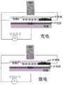
图2是本发明器件的工作原理图。为简单起见,我们以半导体层为P型半导体,且该能源转换器件处于短路时的情形为例加以说明。当在电极1和电极3之间施加交流信号时,在电极1和电极2间短路时,该器件会有两个物理过程:1.当电极3相对于电极1(电极2)是负电压时,由于电极1和半导体是欧姆接触,电极2和半导体时肖特基接触,空穴会主要从电极1注入到半导体中,此为充电过程;2.当电极3相对于电极1是正电压时,半导体中的空穴会向外电路释放,此时对空穴电极1和电极2处均可顺畅流通,因此空穴几乎平均地从两个电极流出,此为放电过程。因此,在一个交流电压周期内,有净电荷从电极1流向电极2,形成直流电流。Fig. 2 is a working principle diagram of the device of the present invention. For simplicity, we take the case where the semiconductor layer is a P-type semiconductor and the energy conversion device is short-circuited as an example for description. When an AC signal is applied between electrode 1 and electrode 3, when there is a short circuit between electrode 1 and electrode 2, the device will have two physical processes: 1. When electrode 3 is a negative voltage relative to electrode 1 (electrode 2) , since the electrode 1 and the semiconductor are in ohmic contact, and the electrode 2 is in Schottky contact with the semiconductor, the holes will mainly be injected from the electrode 1 into the semiconductor, which is the charging process; 2. When the electrode 3 is a positive voltage relative to the electrode 1, The holes in the semiconductor will be released to the external circuit. At this time, both the hole-to-hole electrode 1 and the electrode 2 can flow smoothly, so the holes flow out from the two electrodes almost evenly, which is the discharge process. Therefore, in one AC voltage cycle, there is a net charge flowing from electrode 1 to electrode 2, forming a DC current.
显然,在电极1和电极2之间形成的直流电流与所施加的交流信号的频率与幅值相关。幅值越大,频率越高,则电极1和电极2之间的直流电流越大。另外,该能源转换器件的性能与器件自身的特性有关。具体来说,当介电层的介电常数越大,厚度越薄,即介电层单位面积电容越大时,同样的交流信号下器件具有更大的短路电流和开路电压,具有高的转换效率。当半导体的迁移率越高时,器件能够响应更高频率的交流信号,因此可以收集更宽频域的电磁波信号。此外,肖特基结的整流特性越强,器件的转换效率也越高。Obviously, the DC current formed between electrode 1 and electrode 2 is related to the frequency and amplitude of the applied AC signal. The larger the amplitude and the higher the frequency, the greater the DC current between electrode 1 and electrode 2. In addition, the performance of the energy conversion device is related to the characteristics of the device itself. Specifically, when the dielectric constant of the dielectric layer is larger and the thickness is thinner, that is, the capacitance per unit area of the dielectric layer is larger, the device has a larger short-circuit current and open-circuit voltage under the same AC signal, and has a high conversion rate. efficiency. When the mobility of the semiconductor is higher, the device can respond to higher frequency AC signals, so it can collect electromagnetic wave signals in a wider frequency range. In addition, the stronger the rectification characteristics of the Schottky junction, the higher the conversion efficiency of the device.
图3是用该器件与天线结合用来收集电磁波能量的示意图。该能源转换器件不仅可应用于收集大气中的电磁波信号,转换成可用的直流电用于驱动小功率器件或给能源储存器件(如电池、电容)等充电,也可用于射频识别标签的电源驱动等。Figure 3 is a schematic diagram of using the device in combination with an antenna to collect electromagnetic wave energy. The energy conversion device can not only be used to collect electromagnetic wave signals in the atmosphere, convert it into usable direct current to drive low-power devices or charge energy storage devices (such as batteries, capacitors), etc., but also can be used for the power drive of radio frequency identification tags, etc. .
Claims (8)
Priority Applications (1)
| Application Number | Priority Date | Filing Date | Title |
|---|---|---|---|
| CN201810388951.9ACN109166941B (en) | 2018-04-26 | 2018-04-26 | an energy conversion device |
Applications Claiming Priority (1)
| Application Number | Priority Date | Filing Date | Title |
|---|---|---|---|
| CN201810388951.9ACN109166941B (en) | 2018-04-26 | 2018-04-26 | an energy conversion device |
Publications (2)
| Publication Number | Publication Date |
|---|---|
| CN109166941A CN109166941A (en) | 2019-01-08 |
| CN109166941Btrue CN109166941B (en) | 2020-07-24 |
Family
ID=64897107
Family Applications (1)
| Application Number | Title | Priority Date | Filing Date |
|---|---|---|---|
| CN201810388951.9AActiveCN109166941B (en) | 2018-04-26 | 2018-04-26 | an energy conversion device |
Country Status (1)
| Country | Link |
|---|---|
| CN (1) | CN109166941B (en) |
Families Citing this family (2)
| Publication number | Priority date | Publication date | Assignee | Title |
|---|---|---|---|---|
| CN112578189A (en)* | 2019-09-27 | 2021-03-30 | 中国科学院物理研究所 | Self-driven photoelectric detection system |
| CN115021609B (en)* | 2022-04-13 | 2025-08-29 | 北京纳米能源与系统研究所 | An energy generator |
Family Cites Families (6)
| Publication number | Priority date | Publication date | Assignee | Title |
|---|---|---|---|---|
| US9178369B2 (en)* | 2011-01-18 | 2015-11-03 | Mojo Mobility, Inc. | Systems and methods for providing positioning freedom, and support of different voltages, protocols, and power levels in a wireless power system |
| US9401436B2 (en)* | 2011-05-05 | 2016-07-26 | Qualcomm Incorporated | Multiple control transcap variable capacitor |
| US9793685B2 (en)* | 2011-05-24 | 2017-10-17 | The Regents Of The University Of California | Junctionless semiconductor light emitting devices |
| CN102868233A (en)* | 2011-07-06 | 2013-01-09 | 李梦轲 | Nano power generator |
| CN102723367B (en)* | 2012-06-29 | 2015-02-11 | 昆山工研院新型平板显示技术中心有限公司 | Oxide semiconductor thin film transistor |
| CN106981897A (en)* | 2017-03-24 | 2017-07-25 | 西安蜂语信息科技有限公司 | wireless charging method, device, system and Bluetooth earphone |
- 2018
- 2018-04-26CNCN201810388951.9Apatent/CN109166941B/enactiveActive
Also Published As
| Publication number | Publication date |
|---|---|
| CN109166941A (en) | 2019-01-08 |
Similar Documents
| Publication | Publication Date | Title |
|---|---|---|
| JP2018129500A5 (en) | ||
| CN107332462A (en) | The self-powered piezoelectric vibration energy that can track maximum power point extracts circuit | |
| CN103715920A (en) | Rectifier circuit and radio frequency identification tag circuit chip comprising the same | |
| CN109166941B (en) | an energy conversion device | |
| CN104465796A (en) | Kind mixing GaAs terahertz schottky third harmonic generation diode | |
| KR101226340B1 (en) | Organic rectifier | |
| Yeo et al. | Comparison of CMOS rectifiers for micropower energy harvesters | |
| Salter et al. | RF energy scavenging system utilising switched capacitor DC-DC converter | |
| Guo et al. | Class F rectifier RF-DC conversion efficiency analysis | |
| Semsudin et al. | Designing a boost converter of micro energy harvester using thermal and vibration input for biomedical devices | |
| CN104320124B (en) | A kind of self-powered interface circuit collected for thermoelectric energy | |
| WO2018064893A1 (en) | Light enhanced vibration energy harvesting device and array | |
| singh Chouhan et al. | A modified cross coupled rectifier based charge pump for energy harvesting using RF to DC conversion | |
| Gao et al. | A 50–60 GHz rectifier with− 7dBm sensitivity for 1 V DC output voltage and 8% efficiency in 65-nm CMOS | |
| Chang et al. | A high-performance AC-DC rectifier with fully actively controlled switches for vibration energy harvesting | |
| CN204204868U (en) | Class mixing GaAs Terahertz Schottky frequency tripling diode | |
| CN106653868A (en) | Self-balanced terahertz Schottky barrier diode | |
| CN208173591U (en) | Field-effect diode and full-wave bridge and energy management circuit including it | |
| CN103199131B (en) | A kind of electric-field enhancing type schottky junction solar battery structure | |
| CN115133671A (en) | System for wireless charging mobile phone by taking radio waves as energy | |
| Sampe et al. | Ultra low power hybrid micro energy harvester using rf, thermal and vibration for biomedical devices | |
| CN107508490A (en) | A kind of piezoelectric vibration energy extracts circuit | |
| CN202385029U (en) | Piezoelectric energy accumulating device | |
| CN203706243U (en) | A rectification circuit and a radio-frequency identification label chip including the rectification circuit | |
| El Mouzouade et al. | Analysis and design of an active rectifier for wireless power transfer in 90 nm CMOS technology |
Legal Events
| Date | Code | Title | Description |
|---|---|---|---|
| PB01 | Publication | ||
| PB01 | Publication | ||
| SE01 | Entry into force of request for substantive examination | ||
| SE01 | Entry into force of request for substantive examination | ||
| GR01 | Patent grant | ||
| GR01 | Patent grant |