CN109148598B - Thin film transistor and preparation method thereof - Google Patents
Thin film transistor and preparation method thereofDownload PDFInfo
- Publication number
- CN109148598B CN109148598BCN201810949812.9ACN201810949812ACN109148598BCN 109148598 BCN109148598 BCN 109148598BCN 201810949812 ACN201810949812 ACN 201810949812ACN 109148598 BCN109148598 BCN 109148598B
- Authority
- CN
- China
- Prior art keywords
- channel region
- active layer
- layer
- gate
- substrate
- Prior art date
- Legal status (The legal status is an assumption and is not a legal conclusion. Google has not performed a legal analysis and makes no representation as to the accuracy of the status listed.)
- Active
Links
Images


Classifications
- H—ELECTRICITY
- H10—SEMICONDUCTOR DEVICES; ELECTRIC SOLID-STATE DEVICES NOT OTHERWISE PROVIDED FOR
- H10D—INORGANIC ELECTRIC SEMICONDUCTOR DEVICES
- H10D30/00—Field-effect transistors [FET]
- H10D30/60—Insulated-gate field-effect transistors [IGFET]
- H10D30/67—Thin-film transistors [TFT]
- H10D30/674—Thin-film transistors [TFT] characterised by the active materials
- H10D30/6755—Oxide semiconductors, e.g. zinc oxide, copper aluminium oxide or cadmium stannate
- H10D30/6756—Amorphous oxide semiconductors
- G—PHYSICS
- G02—OPTICS
- G02F—OPTICAL DEVICES OR ARRANGEMENTS FOR THE CONTROL OF LIGHT BY MODIFICATION OF THE OPTICAL PROPERTIES OF THE MEDIA OF THE ELEMENTS INVOLVED THEREIN; NON-LINEAR OPTICS; FREQUENCY-CHANGING OF LIGHT; OPTICAL LOGIC ELEMENTS; OPTICAL ANALOGUE/DIGITAL CONVERTERS
- G02F1/00—Devices or arrangements for the control of the intensity, colour, phase, polarisation or direction of light arriving from an independent light source, e.g. switching, gating or modulating; Non-linear optics
- G02F1/01—Devices or arrangements for the control of the intensity, colour, phase, polarisation or direction of light arriving from an independent light source, e.g. switching, gating or modulating; Non-linear optics for the control of the intensity, phase, polarisation or colour
- G02F1/13—Devices or arrangements for the control of the intensity, colour, phase, polarisation or direction of light arriving from an independent light source, e.g. switching, gating or modulating; Non-linear optics for the control of the intensity, phase, polarisation or colour based on liquid crystals, e.g. single liquid crystal display cells
- G02F1/133—Constructional arrangements; Operation of liquid crystal cells; Circuit arrangements
- G02F1/136—Liquid crystal cells structurally associated with a semi-conducting layer or substrate, e.g. cells forming part of an integrated circuit
- G02F1/1362—Active matrix addressed cells
- G02F1/1368—Active matrix addressed cells in which the switching element is a three-electrode device
- H—ELECTRICITY
- H10—SEMICONDUCTOR DEVICES; ELECTRIC SOLID-STATE DEVICES NOT OTHERWISE PROVIDED FOR
- H10D—INORGANIC ELECTRIC SEMICONDUCTOR DEVICES
- H10D30/00—Field-effect transistors [FET]
- H10D30/60—Insulated-gate field-effect transistors [IGFET]
- H10D30/67—Thin-film transistors [TFT]
- H10D30/6757—Thin-film transistors [TFT] characterised by the structure of the channel, e.g. transverse or longitudinal shape or doping profile
- H—ELECTRICITY
- H10—SEMICONDUCTOR DEVICES; ELECTRIC SOLID-STATE DEVICES NOT OTHERWISE PROVIDED FOR
- H10D—INORGANIC ELECTRIC SEMICONDUCTOR DEVICES
- H10D62/00—Semiconductor bodies, or regions thereof, of devices having potential barriers
- H10D62/10—Shapes, relative sizes or dispositions of the regions of the semiconductor bodies; Shapes of the semiconductor bodies
- H10D62/17—Semiconductor regions connected to electrodes not carrying current to be rectified, amplified or switched, e.g. channel regions
- H10D62/213—Channel regions of field-effect devices
- H10D62/221—Channel regions of field-effect devices of FETs
- H10D62/235—Channel regions of field-effect devices of FETs of IGFETs
- H—ELECTRICITY
- H10—SEMICONDUCTOR DEVICES; ELECTRIC SOLID-STATE DEVICES NOT OTHERWISE PROVIDED FOR
- H10D—INORGANIC ELECTRIC SEMICONDUCTOR DEVICES
- H10D99/00—Subject matter not provided for in other groups of this subclass
Landscapes
- Physics & Mathematics (AREA)
- Nonlinear Science (AREA)
- Engineering & Computer Science (AREA)
- Microelectronics & Electronic Packaging (AREA)
- Mathematical Physics (AREA)
- Chemical & Material Sciences (AREA)
- Crystallography & Structural Chemistry (AREA)
- General Physics & Mathematics (AREA)
- Optics & Photonics (AREA)
- Thin Film Transistor (AREA)
Abstract
Translated fromChinese
Description
Translated fromChinese技术领域technical field
本发明涉及液晶显示领域,尤其涉及一种薄膜晶体管及其制备方法。The invention relates to the field of liquid crystal display, in particular to a thin film transistor and a preparation method thereof.
背景技术Background technique
随着液晶显示器尺寸的不断增大,驱动频率也不断提高,传统非晶硅薄膜晶体管的电子迁移率(迁移率为单位电场下电子的平均漂移速度)很难满足需求,而且均一性差。铟镓锌氧化物(indium gallium zinc oxide,IGZO)是一种含有铟、镓和锌的非晶氧化物,其具有高迁移率,载流子迁移率是非晶硅的20~30倍。以铟镓锌氧化物等半导体氧化物材料作为有源层的金属氧化物薄膜晶体管大大提高了薄膜晶体管对像素电极的充放电速率,具有高开态电流、低关态电流,可以迅速开关,提高像素的响应速度,实现更快的刷新率,且金属氧化物薄膜晶体管具有低的工艺温度、大的电子迁移率、优良的均匀性和表面平坦性等。其缺点在于,由于半导体氧化物对环境比较敏感,因此在稳定性方面性能较差With the continuous increase in the size of liquid crystal displays and the continuous increase in driving frequency, the electron mobility of traditional amorphous silicon thin film transistors (mobility is the average drift speed of electrons under a unit electric field) is difficult to meet the demand, and the uniformity is poor. Indium gallium zinc oxide (IGZO) is an amorphous oxide containing indium, gallium and zinc, which has high mobility, and the carrier mobility is 20-30 times that of amorphous silicon. The metal oxide thin film transistor using semiconductor oxide materials such as indium gallium zinc oxide as the active layer greatly improves the charge and discharge rate of the thin film transistor to the pixel electrode. The response speed of the pixel achieves a faster refresh rate, and the metal oxide thin film transistor has a low process temperature, large electron mobility, excellent uniformity and surface flatness, etc. The disadvantage is that the semiconductor oxide has poor performance in terms of stability due to its sensitivity to the environment
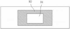
图1是现有的具有底栅结构的金属氧化物薄膜晶体管的结构示意图。请参阅图1,在制作金属氧化物薄膜晶体管时,半导体氧化物有源层10通常采用湿法刻蚀形成,而源漏极11也是采用湿法刻蚀形成,因此,在制作源漏极11时,湿法刻蚀会对半导体氧化物有源层10造成损伤。例如,制作源漏极11时的湿法刻蚀工艺会对在沟道区12内源漏极11与半导体氧化物有源层10重叠区域(如图1中A区域)的半导体氧化物有源层10造成损伤,从而影响器件性能。为了避免在形成源漏极10时的湿刻对沟道区12内的半导体氧化物有源层10造成损伤而影响器件性能,需要在沟道区12上方增加制作刻蚀阻挡层13(Etching-Stop-Layer,简称ESL)。然而,所述刻蚀阻挡层13的制作会增加制作工艺的复杂性,并且不利于降低成本。FIG. 1 is a schematic structural diagram of a conventional metal oxide thin film transistor with a bottom gate structure. Please refer to FIG. 1 , in the manufacture of metal oxide thin film transistors, the semiconductor oxide
在薄膜晶体管中,顶栅(Top Gate)结构相比于底栅(Bottom Gate)结构来说,寄生电容小,更适合在大尺寸中应用。并且,如上所述,对于金属氧化物薄膜晶体管,由于源漏极刻蚀对半导体氧化物有影响,则制作具有底栅结构的金属氧化物薄膜晶体管困难较大。In thin film transistors, the top gate structure has smaller parasitic capacitance than the bottom gate structure, and is more suitable for large-scale applications. Furthermore, as mentioned above, for metal oxide thin film transistors, it is difficult to fabricate metal oxide thin film transistors with bottom gate structures due to the influence of source and drain etching on semiconductor oxides.
图2是现有的具有顶栅结构的金属氧化物薄膜晶体管的结构示意图。请参阅图2,在基板23上设置有一半导体氧化物有源层20,在所述半导体氧化物有源层20上方设置有一栅极21,所述栅极21与所述半导体氧化物有源层20的一沟道区22对应设置,具体地说,所述栅极21在所述基板23上的正投影与所述有源层20的沟道区22在所述基板23上的正投影重合。该顶栅结构的薄膜晶体管的缺点在于,在稳定性方面性能较差。FIG. 2 is a schematic structural diagram of a conventional metal oxide thin film transistor with a top-gate structure. Referring to FIG. 2 , a semiconductor oxide
发明内容SUMMARY OF THE INVENTION
本发明所要解决的技术问题是,提供一种薄膜晶体管及其制备方法,其能够提高有源层的迁移率和稳定性,进而提高所述薄膜晶体管的稳定性。The technical problem to be solved by the present invention is to provide a thin film transistor and a preparation method thereof, which can improve the mobility and stability of the active layer, thereby improving the stability of the thin film transistor.
为了解决上述问题,本发明提供了一种薄膜晶体管,包括一有源层及设置在所述有源层上方的一栅极,所述有源层包括一主沟道区及一副沟道区,所述副沟道区围绕所述主沟道区设置,所述栅极与所述主沟道区对应设置,所述副沟道区的载流子的浓度大于所述主沟道区的载流子浓度。In order to solve the above problems, the present invention provides a thin film transistor including an active layer and a gate disposed above the active layer, the active layer including a main channel region and a sub-channel region , the sub-channel region is arranged around the main channel region, the gate is arranged corresponding to the main channel region, and the carrier concentration of the sub-channel region is greater than that of the main channel region carrier concentration.
在一实施例中,所述有源层为半导体氧化物有源层。In one embodiment, the active layer is a semiconductor oxide active layer.
在一实施例中,所述薄膜晶体管还包括一钝化层,所述钝化层自下而上包括一氧化硅层及一氮化硅层。In one embodiment, the thin film transistor further includes a passivation layer, and the passivation layer includes a silicon oxide layer and a silicon nitride layer from bottom to top.
在一实施例中,所述薄膜晶体管还包括一基板、一栅极绝缘层、一钝化层及一源漏极,所述有源层设置在所述基板上,所述栅极绝缘层设置在所述有源层上,所述栅极设置在所述栅极绝缘层上,所述钝化层覆盖所述基板、所述有源层、所述栅极绝缘层及所述栅极,所述源漏极穿过所述钝化层与所述有源层的源区及漏区连接。In one embodiment, the thin film transistor further includes a substrate, a gate insulating layer, a passivation layer, and a source and drain electrode, the active layer is disposed on the substrate, and the gate insulating layer is disposed on the active layer, the gate is disposed on the gate insulating layer, the passivation layer covers the substrate, the active layer, the gate insulating layer and the gate, The source and drain are connected to the source and drain regions of the active layer through the passivation layer.
本发明还提供一种权利要求1所述的薄膜晶体管的制备方法,包括如下步骤:在一基板上形成所述有源层,所述有源层包括一主沟道区及一副沟道区,所述副沟道区围绕所述主沟道区设置;在所述有源层上方形成一栅极,所述栅极对应所述主沟道区设置;对所述有源层进行掺杂,所述副沟道区的载流子的浓度大于所述主沟道区的载流子浓度。The present invention further provides a method for fabricating a thin film transistor according to claim 1, comprising the steps of: forming the active layer on a substrate, the active layer comprising a main channel region and a sub-channel region , the secondary channel region is arranged around the main channel region; a gate is formed above the active layer, the gate is arranged corresponding to the main channel region; the active layer is doped , the carrier concentration of the secondary channel region is greater than the carrier concentration of the main channel region.
在一实施例中,对所述有源层进行掺杂的的方法包括如下步骤:在所述有源层及所述栅极上覆盖一钝化层,所述钝化层自下而上包括一氧化硅层及一氮化硅层,所述氮化硅层中的氢离子扩散至所述副沟道区,进而对所述副沟道区进行掺杂,使得所述副沟道区的载流子的浓度大于所述主沟道区的载流子浓度。In one embodiment, the method for doping the active layer includes the following steps: covering the active layer and the gate with a passivation layer, the passivation layer including from bottom to top A silicon oxide layer and a silicon nitride layer, hydrogen ions in the silicon nitride layer diffuse into the sub-channel region, and then dope the sub-channel region, so that the sub-channel region has The carrier concentration is greater than that of the main channel region.
在一实施例中,在形成钝化层步骤之后,还包括如下步骤:在所述钝化层上开孔,形成贯通至所述有源层的一源区的一源极孔、贯通至所述有源层的一漏区的一漏极孔;沉积一金属层,形成与所述有源层的所述源区的连接的一源极及与所述有源层的所述漏区的连接的一漏极。In one embodiment, after the step of forming the passivation layer, the method further includes the following step: opening a hole on the passivation layer to form a source hole penetrating to a source region of the active layer, penetrating to all a drain hole in a drain region of the active layer; depositing a metal layer to form a source electrode connected to the source region of the active layer and a source electrode connected to the drain region of the active layer connected to a drain.
在一实施例中,对所述有源层进行掺杂的的方法包括如下步骤:对所述有源层进行等离子体处理,使得所述副沟道区的载流子的浓度大于所述主沟道区的载流子浓度。In one embodiment, the method for doping the active layer includes the step of: performing plasma treatment on the active layer, so that the carrier concentration of the sub-channel region is greater than that of the main channel region. carrier concentration in the channel region.
在一实施例中,在对所述有源层进行掺杂步骤之后,还包括如下步骤:在所述有源层及所述栅极上覆盖一钝化层。In one embodiment, after the doping step is performed on the active layer, the following step is further included: covering the active layer and the gate with a passivation layer.
在一实施例中,在所述有源层上方形成所述栅极的步骤之前,还包括如下步骤:在所述有源层表面形成一栅极绝缘层,所述栅极形成在所述栅极绝缘层表面。In one embodiment, before the step of forming the gate over the active layer, the method further includes the following step: forming a gate insulating layer on the surface of the active layer, and the gate is formed on the gate surface of the extremely insulating layer.
本发明的优点在于,增加了未被栅极阻挡的副沟道区,且所述副沟道区的载流子的浓度大于所述主沟道区的载流子浓度,即所述副沟道区的载流子迁移率层高于所述主沟道区的载流子迁移率,本申请形成高迁移率沟道区与低迁移率沟道区搭配的双沟道区结构,提高了有源层的迁移率和稳定性,进而提高所述薄膜晶体管的稳定性。The advantages of the present invention are that the sub-channel region not blocked by the gate is increased, and the carrier concentration of the sub-channel region is greater than that of the main channel region, that is, the sub-channel The carrier mobility layer of the channel region is higher than the carrier mobility of the main channel region, and the present application forms a dual-channel region structure with a high-mobility channel region and a low-mobility channel region, which improves the The mobility and stability of the active layer, thereby improving the stability of the thin film transistor.
附图说明Description of drawings
图1是现有的具有底栅结构的金属氧化物薄膜晶体管的结构示意图;1 is a schematic structural diagram of an existing metal oxide thin film transistor with a bottom gate structure;
图2是现有的具有顶栅结构的金属氧化物薄膜晶体管的结构示意图;2 is a schematic structural diagram of an existing metal oxide thin film transistor with a top-gate structure;
图3A~图3J是本发明薄膜晶体管制备方法的一实施例的流程图;3A to 3J are flowcharts of an embodiment of a method for fabricating a thin film transistor of the present invention;
图4A~图4K是本发明薄膜晶体管制备方法的另一实施例的流程图;4A to 4K are flowcharts of another embodiment of the method for manufacturing a thin film transistor of the present invention;
图5是本发明薄膜晶体管的一实施例的结构示意图;FIG. 5 is a schematic structural diagram of an embodiment of a thin film transistor of the present invention;
图6是本发明薄膜晶体管的一实施例的俯视示意图。FIG. 6 is a schematic top view of an embodiment of the thin film transistor of the present invention.
具体实施方式Detailed ways
下面结合附图对本发明提供的薄膜晶体管及其制备方法的具体实施方式做详细说明。The specific embodiments of the thin film transistor provided by the present invention and the preparation method thereof will be described in detail below with reference to the accompanying drawings.
图3A~图3J是本发明薄膜晶体管制备方法的一实施例的流程图。在该实施例中,本发明薄膜晶体管的制备方法包括如下步骤。3A to 3J are flowcharts of an embodiment of a method for fabricating a thin film transistor of the present invention. In this embodiment, the manufacturing method of the thin film transistor of the present invention includes the following steps.
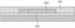
请参阅图3A,提供一基板300。所述基板300可包括硬质基板例如玻璃基板与陶瓷基板、可挠式基板(flexiblesubstrate)例如塑胶基板或其他适合材料所形成的基板。例如,在本实施例中,所述基板100为玻璃基板。在本步骤之后,还包括一在所述基板300上形成缓冲层301的步骤。所述缓冲层301可以为氮化硅或者氧化硅材质,其形成方法可以为化学气相沉积法(CVD)。Referring to FIG. 3A , a
请参阅图3B,在所述基板300上形成一有源层302。在本实施例中,在所述缓冲层301上形成所述有源层302。所述有源层302可以采用半导体氧化物材料制作而成,所述半导体氧化物材料包括但不限于铟镓锌氧化物。具体地说,在缓冲层301上采用沉积等方法形成半导体氧化物层,图形化所述半导体氧化物层,形成所述有源层302。所述有源层302包括一主沟道区B1及一副沟道区B2,所述副沟道区B2包围所述主沟道区B1。其中,图3C为俯视示意图,示意性地绘示出主沟道区B1及一副沟道区B2的位置关系。Referring to FIG. 3B , an
请参阅图3D,在所述有源层302上形成一栅极绝缘层303。具体地说,在本实施例中,使用化学气相沉积的方法在所述缓冲层301及所述有源层302上沉积并图形化形成栅极绝缘层303。其中,所述栅极绝缘层303包括但不限于二氧化硅层或三氧化二铝层。Referring to FIG. 3D , a
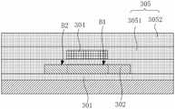
请参阅图3E,在所述栅极绝缘层303上形成一栅极304。具体地说,在本实施例中,在所述缓冲层301、所述有源层302及所述栅极绝缘层303上沉积一金属层(附图中未绘示),图形化所述金属层,进而形成所述栅极304。形成所述栅极304的材料包括但不限于钼或铝。所述栅极304对应所述主沟道区B1设置。具体地说,所述栅极304在所述基板300上的正投影与所述有源层302的主沟道区B1在所述基板300上的正投影重合。图3F为图3E所示结构的俯视示意图,其中栅极304正对主沟道区B1设置。Referring to FIG. 3E , a
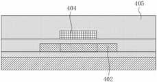
请参阅图3G,对所述有源层302进行掺杂。在本实施例中,对所述有源层302进行掺杂的方法为,在所述有源层302及所述栅极304上覆盖一钝化层305。所述钝化层305自下而上包括一氧化硅层3051及一氮化硅层3052。其中,所述氮化硅层3052富含氢离子,则所述氢离子扩散至所述有源层302。在有源层302处,由于所述栅极304的遮挡作用,仅有少量的所述氢离子扩散至所述主沟道区B1,而所述副沟道区B2没有被栅极304遮挡,则会有大量的所述氢离子扩散至所述副沟道区B2,进而对所述副沟道区B2进行掺杂,使得所述副沟道区B2的自由电子数较多,所述副沟道区B2的载流子的浓度大于所述主沟道区B1的载流子浓度,即所述副沟道区B2的载流子迁移率层高于所述主沟道区B1的载流子迁移率。Referring to FIG. 3G, the
在现有技术中,请参阅图2,栅极21位于所述沟道区22上方,所述沟道区22相当于本申请的主沟道区B1。请继续参阅图3G,本申请相对于图2所示的现有技术,增加了副沟道区B2,且所述副沟道区B2的载流子的浓度大于所述主沟道区B1的载流子浓度,即所述副沟道区B2的载流子迁移率层高于所述主沟道区B1的载流子迁移率,本申请形成高迁移率沟道区与低迁移率沟道区搭配的双沟道区结构,提高了有源层302的迁移率和稳定性。In the prior art, please refer to FIG. 2 , the gate 21 is located above the
请参阅图3H,在所述钝化层305上开孔,形成贯通至所述有源层302的一源区的一源极孔306、贯通至所述有源层302的一漏区的一漏极孔307。具体地说,在本实施例中,采用蚀刻的方法制作所述源极孔306、所述漏极孔307。Referring to FIG. 3H , holes are opened on the
请参阅图3I,沉积一金属层,形成与所述有源层302的所述源区连接的一源极308及与所述有源层302的所述漏区连接的一漏极309。制备所述源极308及所述漏极309的材料与制备所述栅极304的材料相同,包括但不限于钼或铝,进一步,可采用蚀刻等方法图形化所述金属层,进而形成所述源极308及所述漏极309。Referring to FIG. 3I , a metal layer is deposited to form a
进一步,在本实施例中,还包括一形成介电层310的步骤。请参阅图3J,在所述钝化层305表面、源极308表面、漏极309表面形成所述介电层310。所述介电层310包括但不限于二氧化硅层或三氧化铝层,其为本领域常规的结构,不再赘述。Further, in this embodiment, a step of forming a
图4A~图4K是本发明薄膜晶体管制备方法的另一实施例的流程图。在该实施例中,本发明薄膜晶体管的制备方法包括如下步骤。4A to 4K are flowcharts of another embodiment of the method for fabricating a thin film transistor of the present invention. In this embodiment, the manufacturing method of the thin film transistor of the present invention includes the following steps.
请参阅图4A,提供一基板400。所述基板400可包括硬质基板例如玻璃基板与陶瓷基板、可挠式基板(flexiblesubstrate)例如塑胶基板或其他适合材料所形成的基板。例如,在本实施例中,所述基板100为玻璃基板。在本步骤之后,还包括一在所述基板400上形成缓冲层401的步骤。所述缓冲层401可以为氮化硅或者氧化硅材质,其形成方法可以为化学气相沉积法(CVD)。Referring to FIG. 4A , a
请参阅图4B,在所述基板400上形成一有源层402。在本实施例中,在所述缓冲层401上形成所述有源层402。所述有源层402可以采用半导体氧化物材料制作而成,所述半导体氧化物材料包括但不限于铟镓锌氧化物。具体地说,在缓冲层401上采用沉积等方法形成半导体氧化物层,图形化所述半导体氧化物层,形成所述有源层402。所述有源层402包括一主沟道区B1及一副沟道区B2,所述副沟道区B2包围所述主沟道区B1。其中,图4C为俯视示意图,示意性地绘示出主沟道区B1及一副沟道区B2的位置关系。Referring to FIG. 4B , an
请参阅图4D,在所述有源层402上形成一栅极绝缘层404。具体地说,在本实施例中,使用化学气相沉积的方法在所述缓冲层401及所述有源层402上沉积并图形化形成栅极绝缘层403。其中,所述栅极绝缘层403包括但不限于二氧化硅层或三氧化二铝层。Referring to FIG. 4D , a
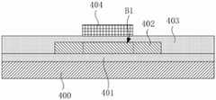
请参阅图4E,在所述栅极绝缘层403上形成一栅极404。具体地说,在本实施例中,在所述缓冲层401、所述有源层402及所述栅极绝缘层403上沉积一金属层(附图中未绘示),图形化所述金属层,进而形成所述栅极404。形成所述栅极404的材料包括但不限于钼或铝。所述栅极404对应所述主沟道区B1设置。具体地说,所述栅极404在所述基板400上的正投影与所述有源层402的主沟道区B1在所述基板400上的正投影重合。图4F为图4E所示结构的俯视示意图,其中栅极404及有源层402采用虚线绘制。Referring to FIG. 4E , a
请参阅图4G,对所述有源层402进行掺杂。在本实施例中,对所述有源层402进行掺杂的方法为:,对所述有源层402进行等离子体处理,使得所述副沟道区B2的载流子的浓度大于所述主沟道区B1的载流子浓度。具体的说,所述等离子体出来包括采用He/H2/NH3等气体对有源层402处理,如图中箭头所示。在本发明其他实施方式中,所述掺杂方法还包括离子注入、Al反应等方式,,其均为本领域常规技术,不再赘述。Referring to FIG. 4G, the
在有源层402处,由于所述栅极404的遮挡作用,仅有少量的所述离子扩散至所述主沟道区B1,而所述副沟道区B2没有被栅极404遮挡,则会有大量的所述离子扩散至所述副沟道区B2,进而对所述副沟道区B2进行掺杂,使得所述副沟道区B2的自由电子数较多,所述副沟道区B2的载流子的浓度大于所述主沟道区B1的载流子浓度,即所述副沟道区B2的载流子迁移率层高于所述主沟道区B1的载流子迁移率。At the
在现有技术中,请参阅图2,栅极21位于所述沟道区22上方,所述沟道区22相当于本申请的主沟道区B1。请继续参阅图4G,本申请相对于图2所示的现有技术,增加了副沟道区B2,且所述副沟道区B2的载流子的浓度大于所述主沟道区B1的载流子浓度,即所述副沟道区B2的载流子迁移率层高于所述主沟道区B1的载流子迁移率,本申请形成高迁移率沟道区与低迁移率沟道区搭配的双沟道区结构,提高了有源层302的迁移率和稳定性。In the prior art, please refer to FIG. 2 , the gate 21 is located above the
请参阅图4H,在所述有源层402及所述栅极404上覆盖一钝化层405。所述钝化层405包括但不限于氧化硅、氮化硅或者二者的组合。Referring to FIG. 4H , a
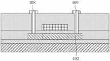
请参阅图4I,在所述钝化层405上开孔,形成贯通至所述有源层402的一源区的一源极孔406、贯通至所述有源层402的一漏区的一漏极孔407。具体地说,在本实施例中,采用蚀刻的方法制作所述源极孔406、所述漏极孔407。Referring to FIG. 4I , holes are formed on the
请参阅图4J,沉积一金属层,形成与所述有源层402的所述源区连接的一源极408及与所述有源层402的所述漏区连接的一漏极409。制备所述源极408及所述漏极409的材料与制备所述栅极404的材料相同,包括但不限于钼或铝,进一步,可采用蚀刻等方法图形化所述金属层,进而形成所述源极408及所述漏极409。Referring to FIG. 4J , a metal layer is deposited to form a
进一步,在本实施例中,还包括一形成介电层410的步骤。请参阅图4K,在所述钝化层405表面、源极408表面、漏极409表面形成所述介电层410。所述介电层410包括但不限于二氧化硅层或三氧化铝层,其为本领域常规的结构,不再赘述。Further, in this embodiment, a step of forming a
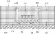
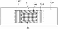
本发明还提供一种薄膜晶体管,其采用上述方法制备。图5是本发明薄膜晶体管的结构示意图,图6是本发明薄膜晶体管的俯视示意图,其中,在图6中采用虚线绘制有源层502及栅极504,请参阅图5及图6,本发明薄膜晶体管包括一基板500、一有源层502及一栅极504。The present invention also provides a thin film transistor prepared by the above method. 5 is a schematic structural diagram of the thin film transistor of the present invention, and FIG. 6 is a schematic top view of the thin film transistor of the present invention, wherein the
所述基板500可包括硬质基板例如玻璃基板与陶瓷基板、可挠式基板(flexiblesubstrate)例如塑胶基板或其他适合材料所形成的基板。例如,在本实施例中,所述基板500为玻璃基板。在本实施例中,在所述基板500上还设置有一缓冲层501,所述缓冲层501可以为氮化硅或者氧化硅材质。The
所述有源层502设置在所述基板500上,在本实施例中,所述有源层502设置在所述缓冲层501上。所述有源层502可以采用半导体氧化物材料制作而成,所述半导体氧化物材料包括但不限于铟镓锌氧化物。所述有源层502包括一主沟道区B1及一副沟道区B2,所述副沟道区B2包围所述主沟道区B1。所述主沟道区B1的载流子浓度小于所述副沟道区B2的载流子的浓度,即所述副沟道区B2的载流子迁移率层高于所述主沟道区B1的载流子迁移率,本申请形成高迁移率沟道区与低迁移率沟道区搭配的双沟道区结构,提高了有源层302的迁移率和稳定性。The
所述栅极504设置在所述有源层502上方。且所述第一栅极504设置在所述主沟道区B1的正上方,即所述栅极504在所述基板500上的正投影与所述有源层502的主沟道区B1在所述基板500上的正投影重合。进一步,所述薄膜晶体管还包括一栅极绝缘层503,所述栅极绝缘层503覆盖所述有源层502,所述栅极504设置在所述栅极绝缘层503表面。所述栅极绝缘层503包括但不限于二氧化硅层或三氧化二铝层。The
所述薄膜晶体管还包括一钝化层505、一源极508、漏极509及一介电层510。所述钝化层505覆盖所述缓冲层501、所述有源层502、所述栅极绝缘层503及所述栅极504。所述源极508及所述漏极509设置在所述钝化层505的表面,且所述源极508及所述漏极509穿过所述钝化层505,与所述有源层502的所述源区及漏区连接。所述介电层510覆盖所述钝化层505表面、源极508表面及漏极509表面。其中,所述钝化层505的材料包括但不限于SiOx、SiNx或两者的组合,所述源极208及所述漏极209的材料包括但不限于钼或铝。所述介电层510但不限于二氧化硅层或三氧化铝层,其为并本领域常规的结构,不再赘述。The thin film transistor further includes a
以上所述仅是本发明的优选实施方式,应当指出,对于本技术领域的普通技术人员,在不脱离本发明原理的前提下,还可以做出若干改进和润饰,这些改进和润饰也应视为本发明的保护范围。The above are only the preferred embodiments of the present invention. It should be pointed out that for those skilled in the art, without departing from the principles of the present invention, several improvements and modifications can also be made, and these improvements and modifications should also be regarded as It is the protection scope of the present invention.
Claims (7)
Translated fromChinesePriority Applications (1)
| Application Number | Priority Date | Filing Date | Title |
|---|---|---|---|
| CN201810949812.9ACN109148598B (en) | 2018-08-20 | 2018-08-20 | Thin film transistor and preparation method thereof |
Applications Claiming Priority (1)
| Application Number | Priority Date | Filing Date | Title |
|---|---|---|---|
| CN201810949812.9ACN109148598B (en) | 2018-08-20 | 2018-08-20 | Thin film transistor and preparation method thereof |
Publications (2)
| Publication Number | Publication Date |
|---|---|
| CN109148598A CN109148598A (en) | 2019-01-04 |
| CN109148598Btrue CN109148598B (en) | 2022-04-26 |
Family
ID=64790590
Family Applications (1)
| Application Number | Title | Priority Date | Filing Date |
|---|---|---|---|
| CN201810949812.9AActiveCN109148598B (en) | 2018-08-20 | 2018-08-20 | Thin film transistor and preparation method thereof |
Country Status (1)
| Country | Link |
|---|---|
| CN (1) | CN109148598B (en) |
Families Citing this family (3)
| Publication number | Priority date | Publication date | Assignee | Title |
|---|---|---|---|---|
| CN113327989B (en)* | 2021-05-19 | 2022-05-17 | 厦门天马微电子有限公司 | Thin film transistor, array substrate, display panel and display device |
| CN116314017B (en)* | 2023-05-18 | 2023-10-27 | 长鑫存储技术有限公司 | Semiconductor structure and manufacturing method thereof |
| CN118969800A (en)* | 2024-07-26 | 2024-11-15 | 武汉华星光电技术有限公司 | Array substrate and display panel |
Family Cites Families (10)
| Publication number | Priority date | Publication date | Assignee | Title |
|---|---|---|---|---|
| JP3474091B2 (en)* | 1997-12-22 | 2003-12-08 | シャープ株式会社 | Semiconductor device and manufacturing method thereof |
| JP3522216B2 (en)* | 2000-12-19 | 2004-04-26 | シャープ株式会社 | Thin film transistor, method of manufacturing the same, and liquid crystal display |
| JP5110803B2 (en)* | 2006-03-17 | 2012-12-26 | キヤノン株式会社 | FIELD EFFECT TRANSISTOR USING OXIDE FILM FOR CHANNEL AND METHOD FOR MANUFACTURING THE SAME |
| KR101282897B1 (en)* | 2008-07-08 | 2013-07-05 | 엘지디스플레이 주식회사 | Poly Silicon Thin Film Transistor and Method of fabricating the same |
| US9112037B2 (en)* | 2012-02-09 | 2015-08-18 | Semiconductor Energy Laboratory Co., Ltd. | Semiconductor device |
| CN103915508B (en)* | 2013-01-17 | 2017-05-17 | 上海天马微电子有限公司 | Oxide thin film transistor with bottom gate structure and manufacturing method thereof |
| KR102188067B1 (en)* | 2014-05-27 | 2020-12-07 | 엘지디스플레이 주식회사 | Thin Film Transistor Array Substrate and Method for Manufacturing the Same |
| CN107195672B (en)* | 2017-05-27 | 2019-12-10 | 京东方科技集团股份有限公司 | A kind of thin film transistor and its control method |
| CN108054172B (en)* | 2017-11-30 | 2020-09-25 | 武汉天马微电子有限公司 | Array substrate, manufacturing method thereof and display device |
| CN107895726A (en)* | 2017-11-30 | 2018-04-10 | 武汉天马微电子有限公司 | Array substrate, manufacturing method thereof and display device |
- 2018
- 2018-08-20CNCN201810949812.9Apatent/CN109148598B/enactiveActive
Also Published As
| Publication number | Publication date |
|---|---|
| CN109148598A (en) | 2019-01-04 |
Similar Documents
| Publication | Publication Date | Title |
|---|---|---|
| CN109920856B (en) | Thin film transistor and its manufacturing method, array substrate and display device | |
| CN107994066B (en) | TFT, manufacturing method, array substrate, display panel and device | |
| CN106158978A (en) | Thin film transistor (TFT), array base palte and preparation method thereof | |
| WO2019061813A1 (en) | Esl-type tft substrate and manufacturing method therefor | |
| CN109148598B (en) | Thin film transistor and preparation method thereof | |
| CN105938800A (en) | Thin film transistor manufacture method and array substrate manufacture method | |
| US20140183541A1 (en) | Thin film transistor, manufacturing method thereof, array substrate and display device | |
| US10170506B2 (en) | LTPS array substrate and method for producing the same | |
| CN107564966B (en) | Thin film transistor, method for manufacturing thin film transistor, and liquid crystal display panel | |
| US9478665B2 (en) | Thin film transistor, method of manufacturing the same, display substrate and display apparatus | |
| CN105629598A (en) | FFS mode array substrate and manufacturing method | |
| CN109148597A (en) | Thin film transistor (TFT) and preparation method thereof | |
| US20150060843A1 (en) | Display substrate and method of manufacturing a display substrate | |
| CN103762246B (en) | A kind of membrane transistor FET and its manufacture method | |
| CN106783734B (en) | A kind of low temperature polycrystalline silicon array substrate and preparation method thereof | |
| CN109103105A (en) | Thin film transistor, preparation method thereof and display device | |
| CN107833893A (en) | Array base palte and preparation method thereof, display panel | |
| US10205026B2 (en) | Thin film transistor having a composite metal gate layer | |
| CN106252277B (en) | Low temperature polysilicon thin film transistor array substrate, manufacturing method and display device | |
| WO2020113622A1 (en) | Method for manufacturing tft substrate, and tft substrate | |
| CN115411054A (en) | Array substrate, preparation method thereof and display device | |
| CN209641659U (en) | A kind of board structure promoting TFT stability | |
| CN107910378A (en) | LTPS thin film transistor (TFT)s, array base palte and preparation method thereof, display device | |
| CN112242406A (en) | Array substrate, manufacturing method thereof and display device | |
| CN114927532B (en) | Array substrate, manufacturing method thereof, and display panel |
Legal Events
| Date | Code | Title | Description |
|---|---|---|---|
| PB01 | Publication | ||
| PB01 | Publication | ||
| SE01 | Entry into force of request for substantive examination | ||
| SE01 | Entry into force of request for substantive examination | ||
| CB02 | Change of applicant information | Address after:9-2 Tangming Avenue, Guangming New District, Shenzhen City, Guangdong Province Applicant after:TCL China Star Optoelectronics Technology Co.,Ltd. Address before:9-2 Tangming Avenue, Guangming New District, Shenzhen City, Guangdong Province Applicant before:Shenzhen China Star Optoelectronics Technology Co.,Ltd. | |
| CB02 | Change of applicant information | ||
| GR01 | Patent grant | ||
| GR01 | Patent grant | ||
| PE01 | Entry into force of the registration of the contract for pledge of patent right | Denomination of invention:Thin film transistors and their preparation methods Effective date of registration:20231113 Granted publication date:20220426 Pledgee:Industrial and Commercial Bank of China Limited Shenzhen Guangming Sub branch Pledgor:TCL China Star Optoelectronics Technology Co.,Ltd. Registration number:Y2023980065368 | |
| PE01 | Entry into force of the registration of the contract for pledge of patent right |