CN109148543B - A pixel structure and display panel - Google Patents
A pixel structure and display panelDownload PDFInfo
- Publication number
- CN109148543B CN109148543BCN201811004317.7ACN201811004317ACN109148543BCN 109148543 BCN109148543 BCN 109148543BCN 201811004317 ACN201811004317 ACN 201811004317ACN 109148543 BCN109148543 BCN 109148543B
- Authority
- CN
- China
- Prior art keywords
- pixel
- sub
- pixels
- unit
- units
- Prior art date
- Legal status (The legal status is an assumption and is not a legal conclusion. Google has not performed a legal analysis and makes no representation as to the accuracy of the status listed.)
- Active
Links
Images


Classifications
- H—ELECTRICITY
- H10—SEMICONDUCTOR DEVICES; ELECTRIC SOLID-STATE DEVICES NOT OTHERWISE PROVIDED FOR
- H10K—ORGANIC ELECTRIC SOLID-STATE DEVICES
- H10K59/00—Integrated devices, or assemblies of multiple devices, comprising at least one organic light-emitting element covered by group H10K50/00
- H10K59/30—Devices specially adapted for multicolour light emission
- H10K59/35—Devices specially adapted for multicolour light emission comprising red-green-blue [RGB] subpixels
- H10K59/351—Devices specially adapted for multicolour light emission comprising red-green-blue [RGB] subpixels comprising more than three subpixels, e.g. red-green-blue-white [RGBW]
- H—ELECTRICITY
- H10—SEMICONDUCTOR DEVICES; ELECTRIC SOLID-STATE DEVICES NOT OTHERWISE PROVIDED FOR
- H10K—ORGANIC ELECTRIC SOLID-STATE DEVICES
- H10K59/00—Integrated devices, or assemblies of multiple devices, comprising at least one organic light-emitting element covered by group H10K50/00
- H10K59/30—Devices specially adapted for multicolour light emission
- H10K59/35—Devices specially adapted for multicolour light emission comprising red-green-blue [RGB] subpixels
- H10K59/352—Devices specially adapted for multicolour light emission comprising red-green-blue [RGB] subpixels the areas of the RGB subpixels being different
- H—ELECTRICITY
- H10—SEMICONDUCTOR DEVICES; ELECTRIC SOLID-STATE DEVICES NOT OTHERWISE PROVIDED FOR
- H10K—ORGANIC ELECTRIC SOLID-STATE DEVICES
- H10K59/00—Integrated devices, or assemblies of multiple devices, comprising at least one organic light-emitting element covered by group H10K50/00
- H10K59/30—Devices specially adapted for multicolour light emission
- H10K59/35—Devices specially adapted for multicolour light emission comprising red-green-blue [RGB] subpixels
- H10K59/353—Devices specially adapted for multicolour light emission comprising red-green-blue [RGB] subpixels characterised by the geometrical arrangement of the RGB subpixels
- H—ELECTRICITY
- H10—SEMICONDUCTOR DEVICES; ELECTRIC SOLID-STATE DEVICES NOT OTHERWISE PROVIDED FOR
- H10K—ORGANIC ELECTRIC SOLID-STATE DEVICES
- H10K71/00—Manufacture or treatment specially adapted for the organic devices covered by this subclass
- H10K71/10—Deposition of organic active material
- H10K71/16—Deposition of organic active material using physical vapour deposition [PVD], e.g. vacuum deposition or sputtering
- H10K71/164—Deposition of organic active material using physical vapour deposition [PVD], e.g. vacuum deposition or sputtering using vacuum deposition
- H—ELECTRICITY
- H10—SEMICONDUCTOR DEVICES; ELECTRIC SOLID-STATE DEVICES NOT OTHERWISE PROVIDED FOR
- H10K—ORGANIC ELECTRIC SOLID-STATE DEVICES
- H10K71/00—Manufacture or treatment specially adapted for the organic devices covered by this subclass
- H10K71/10—Deposition of organic active material
- H10K71/16—Deposition of organic active material using physical vapour deposition [PVD], e.g. vacuum deposition or sputtering
- H10K71/166—Deposition of organic active material using physical vapour deposition [PVD], e.g. vacuum deposition or sputtering using selective deposition, e.g. using a mask
Landscapes
- Engineering & Computer Science (AREA)
- Manufacturing & Machinery (AREA)
- Electroluminescent Light Sources (AREA)
- Devices For Indicating Variable Information By Combining Individual Elements (AREA)
Abstract
Description
Translated fromChinese技术领域technical field
本发明涉及显示技术领域,尤指一种像素结构及显示面板。The present invention relates to the field of display technology, in particular to a pixel structure and a display panel.
背景技术Background technique
有机发光二极管(Organic Light Emitting Diode,OLED)具有主动发光、视角大、色域广、响应快、对比度高的显示特性,且具有轻薄、柔性、节能等优点,已成为最具潜力的新型平板显示技术。Organic Light Emitting Diode (OLED) has the display characteristics of active light emission, large viewing angle, wide color gamut, fast response, high contrast, and has the advantages of lightness, flexibility, energy saving, etc., and has become the most potential new flat panel display. technology.
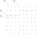
现有技术中,如图1所示,有机发光二极管像素排列结构通常由三个子像素行为一个重复单元,每一重复单元中包含红色子像素(R)、绿色子像素(G)和蓝色子像素(B),第一子像素行两个R子像素和两个G子像素间隔排列,第二子像素行与第一子像素行排列相同,第三子像素行为B子像素。每一像素排列中四个R子像素共用一个掩膜版开口(如图中虚线框B所示),四个G子像素共用一个掩膜版开口(如图中虚线框A所示)。In the prior art, as shown in FIG. 1 , an organic light emitting diode pixel arrangement structure usually consists of three sub-pixels as a repeating unit, and each repeating unit includes a red sub-pixel (R), a green sub-pixel (G) and a blue sub-pixel. For pixel (B), two R sub-pixels and two G sub-pixels in the first sub-pixel row are arranged at intervals, the second sub-pixel row is the same as the first sub-pixel row, and the third sub-pixel row is B sub-pixels. In each pixel arrangement, four R sub-pixels share one mask opening (as shown by the dotted box B in the figure), and four G sub-pixels share one mask opening (as shown by the dotted box A in the figure).
OLED器件中的发光层一般采用蒸镀的方式制作,在蒸镀工艺过程中,采用精细金属掩膜板(Fine Metal Mask,FMM)进行遮挡,因而发光材料按照掩膜板的开口形状被蒸镀到背板玻璃的指定位置,一般掩膜版上的一个开口对应OLED器件像素结构中的一个子像素。然而,虽然上述像素排列结构中R子像素、G子像素可以分别共用掩膜板开口,能够增大其掩膜板开口,但是其B子像素在一条直线上,不仅使其对应的金属掩膜板rib(开口边界距离)较小,同时由于不同颜色子像素排布不均匀,存在发光效果较差的缺陷。The light-emitting layer in an OLED device is generally produced by evaporation. During the evaporation process, a fine metal mask (FMM) is used for shielding, so the light-emitting material is evaporated according to the opening shape of the mask. To the designated position of the back glass, generally an opening on the mask corresponds to a sub-pixel in the pixel structure of the OLED device. However, although the R sub-pixels and the G sub-pixels in the above-mentioned pixel arrangement can share the mask opening respectively, which can increase the mask opening, the B sub-pixels are on a straight line, which not only makes the corresponding metal mask The board rib (opening boundary distance) is small, and at the same time, due to the uneven arrangement of sub-pixels of different colors, there is a defect that the light-emitting effect is poor.
发明内容SUMMARY OF THE INVENTION
本发明实施例提供了一种像素结构及显示面板,用以解决现有技术中存在的发光效果较差的问题,提高产品良率。Embodiments of the present invention provide a pixel structure and a display panel, which are used to solve the problem of poor light-emitting effect in the prior art and improve product yield.
本发明提供了一种像素结构,包括:多个呈阵列排布的重复单元;The invention provides a pixel structure, comprising: a plurality of repeating units arranged in an array;
每一个所述重复单元包括至少一个像素单元,每一所述像素单元中包括四个子像素,所述四个子像素中包括不同颜色的一个第一子像素、一个第二子像素和两个第三子像素,所述第一子像素和第二子像素位于所述像素单元的对角位置,所述两个第三子像素位于所述像素单元的另一对角位置;Each of the repeating units includes at least one pixel unit, each of the pixel units includes four sub-pixels, and the four sub-pixels include a first sub-pixel, a second sub-pixel and two third sub-pixels of different colors sub-pixels, wherein the first sub-pixel and the second sub-pixel are located at diagonal positions of the pixel unit, and the two third sub-pixels are located at another diagonal position of the pixel unit;
相邻的像素单元包括至少一个子像素组,所述子像素组包括相邻且颜色相同的两个子像素。Adjacent pixel units include at least one sub-pixel group, and the sub-pixel group includes two adjacent sub-pixels with the same color.
在上述像素结构中,由于每一像素单元中包括四个子像素,四个子像素中包括不同颜色的第一子像素、第二子像素和两第三子像素,并且第一子像素和第二子像素位于像素单元的对角位置,两个第三子像素位于像素单元的另一对角位置,使得每一像素单元内的子像素排布均匀,而且每一个重复单元包括至少一个像素单元,并以重复单元的形式阵列排布,使得整体像素结构的发光效果较好,提高产品良率;同时由于子像素组包括相邻且颜色相同的两个子像素,相邻的像素单元包括至少一个子像素组,使得相邻的像素单元中的两个子像素共用一个金属掩膜板开口,从而增大了掩膜板的开口,降低对位难度,增大掩膜板的rib,增强了掩膜板的强度,能有效减小掩膜板的厚度,从而降低阴影,减小混色,提高产品良率。In the above pixel structure, since each pixel unit includes four sub-pixels, the four sub-pixels include a first sub-pixel, a second sub-pixel and two third sub-pixels of different colors, and the first sub-pixel and the second sub-pixel The pixel is located at the diagonal position of the pixel unit, and the two third sub-pixels are located at the other diagonal position of the pixel unit, so that the sub-pixels in each pixel unit are evenly arranged, and each repeating unit includes at least one pixel unit, and The array is arranged in the form of repeating units, so that the overall pixel structure has a better luminous effect and improves product yield; at the same time, since the sub-pixel group includes two adjacent sub-pixels with the same color, adjacent pixel units include at least one sub-pixel group, so that two sub-pixels in adjacent pixel units share a metal mask opening, thereby increasing the opening of the mask, reducing the difficulty of alignment, increasing the rib of the mask, and enhancing the mask. The strength can effectively reduce the thickness of the mask plate, thereby reducing shadows, reducing color mixing, and improving product yield.
优选地,每一重复单元由四个呈方阵排布的像素单元组成,其中,在行方向上的两个像素单元镜像设置,和/或,在列方向上的两个像素单元镜像设置。Preferably, each repeating unit consists of four pixel units arranged in a square matrix, wherein two pixel units in the row direction are arranged in mirror images, and/or two pixel units in the column direction are arranged in mirror images.
优选地,每一重复单元由两个像素单元组成,所述两个像素单元在行方向上或列方向上镜像设置。Preferably, each repeating unit is composed of two pixel units, the two pixel units being mirrored in the row direction or the column direction.
优选地,每一重复单元由一个像素单元组成,在列方向上相邻的两个所述像素单元错位设置。Preferably, each repeating unit consists of one pixel unit, and two adjacent pixel units in the column direction are staggered.
优选地,每一个所述像素单元中的第一子像素和第二子像素的大小相同,第一子像素的大小为第三子像素的二倍。Preferably, the size of the first sub-pixel and the second sub-pixel in each of the pixel units is the same, and the size of the first sub-pixel is twice that of the third sub-pixel.
优选地,在列方向上相邻的两个所述像素单元在列方向上错开个所述像素单元的宽度。Preferably, the two adjacent pixel units in the column direction are staggered by the width of the pixel unit in the column direction.
优选地,所述第三子像素的形状为正方形。Preferably, the shape of the third sub-pixel is a square.
优选地,一所述第三子像素位于所述像素单元的右上角位置,另一所述第三子像素位于所述像素单元的左下角位置。Preferably, one of the third sub-pixels is located at the upper right corner of the pixel unit, and the other third sub-pixel is located at the lower left corner of the pixel unit.
优选地,所述子像素组采用蒸镀掩膜版上同一个子像素蒸镀开口形成。Preferably, the sub-pixel group is formed by using the same sub-pixel evaporation opening on the evaporation mask.
另外,本发明还提供了一种显示面板,包括:上述任一项所述的像素结构。In addition, the present invention also provides a display panel, comprising: the pixel structure described in any one of the above.
在上述显示面板中,由于像素结构发光效果较好,产品良率较高,因此,具有该像素结构的显示面板的发光效果较好、且产品良率较高。In the above-mentioned display panel, since the pixel structure has better light-emitting effect and higher product yield, the display panel with this pixel structure has better light-emitting effect and higher product yield.
附图说明Description of drawings
图1为现有技术中像素结构的示意图;1 is a schematic diagram of a pixel structure in the prior art;
图2为本发明实施例提供的像素结构的示意图之一;FIG. 2 is one of schematic diagrams of a pixel structure provided by an embodiment of the present invention;
图3为图2中R子像素对应的掩膜版的结构示意图;3 is a schematic structural diagram of a mask corresponding to an R sub-pixel in FIG. 2;
图4为图2中G子像素对应的掩膜版的结构示意图;4 is a schematic structural diagram of a mask corresponding to the G sub-pixel in FIG. 2;
图5为图2中B子像素对应的掩膜版的结构示意图;5 is a schematic structural diagram of a mask corresponding to the B sub-pixel in FIG. 2;
图6为本发明实施例提供的像素结构的示意图之二;FIG. 6 is a second schematic diagram of a pixel structure provided by an embodiment of the present invention;
图7为图6中R子像素对应的掩膜版的结构示意图实施例提供的像素结构的示意图之二;FIG. 7 is the second schematic diagram of the pixel structure provided by the embodiment of the schematic structural diagram of the mask corresponding to the R sub-pixel in FIG. 6;
图8为图6中G子像素对应的掩膜版的结构示意图本发明实施例提供的像素结构的示意图之三;8 is a schematic structural diagram of a mask corresponding to the G sub-pixel in FIG. 6 , the third schematic diagram of a pixel structure provided by an embodiment of the present invention;
图9为图6中B子像素对应的掩膜版的结构示意图;FIG. 9 is a schematic structural diagram of a mask corresponding to the B sub-pixel in FIG. 6;
图10为本发明实施例提供的像素结构的示意图之三;FIG. 10 is a third schematic diagram of a pixel structure provided by an embodiment of the present invention;
图11为图10中R子像素对应的掩膜版的结构示意图;11 is a schematic structural diagram of a mask corresponding to the R sub-pixel in FIG. 10;
图12为图10中G子像素对应的掩膜版的结构示意图;12 is a schematic structural diagram of a mask corresponding to the G sub-pixel in FIG. 10;
图13为图10中B子像素对应的掩膜版的结构示意图;13 is a schematic structural diagram of a mask corresponding to sub-pixel B in FIG. 10;
图14为本发明实施例提供的像素结构的示意图之四;FIG. 14 is a fourth schematic diagram of a pixel structure provided by an embodiment of the present invention;
图15为图14中R子像素对应的掩膜版的结构示意图;15 is a schematic structural diagram of a mask corresponding to the R sub-pixel in FIG. 14;
图16为图14中G子像素对应的掩膜版的结构示意图;16 is a schematic structural diagram of a mask corresponding to the G sub-pixel in FIG. 14;
图17为图14中B子像素对应的掩膜版的结构示意图;FIG. 17 is a schematic structural diagram of a mask corresponding to the B sub-pixel in FIG. 14;
图18为本发明实施例提供的像素结构的示意图之五;FIG. 18 is a fifth schematic diagram of a pixel structure provided by an embodiment of the present invention;
图19为图18中R子像素对应的掩膜版的结构示意图;FIG. 19 is a schematic structural diagram of a mask corresponding to the R sub-pixel in FIG. 18;
图20为图18中G子像素对应的掩膜版的结构示意图;20 is a schematic structural diagram of a mask corresponding to the G sub-pixel in FIG. 18;
图21为图18中B子像素对应的掩膜版的结构示意图。FIG. 21 is a schematic structural diagram of a mask corresponding to the B sub-pixel in FIG. 18 .
具体实施方式Detailed ways
下面将结合本发明实施例中的附图,对本发明实施例中的技术方案进行清楚、完整地描述,显然,所描述的实施例仅仅是本发明一部分实施例,而不是全部的实施例。基于本发明中的实施例,本领域普通技术人员在没有做出创造性劳动前提下所获得的所有其他实施例,都属于本发明保护的范围。The technical solutions in the embodiments of the present invention will be clearly and completely described below with reference to the accompanying drawings in the embodiments of the present invention. Obviously, the described embodiments are only a part of the embodiments of the present invention, but not all of the embodiments. Based on the embodiments of the present invention, all other embodiments obtained by those of ordinary skill in the art without creative efforts shall fall within the protection scope of the present invention.
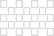
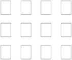
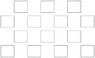
如图2、图6、图10图14以及图18所示,一种像素结构,包括:多个呈阵列排布的重复单元;As shown in FIG. 2, FIG. 6, FIG. 10, FIG. 14 and FIG. 18, a pixel structure includes: a plurality of repeating units arranged in an array;
每一个重复单元包括至少一个像素单元,每一像素单元中包括四个子像素,四个子像素中包括不同颜色的一个第一子像素、一个第二子像素和两个第三子像素,第一子像素和第二子像素位于像素单元的对角位置,两个第三子像素位于像素单元的另一对角位置;Each repeating unit includes at least one pixel unit, each pixel unit includes four sub-pixels, and the four sub-pixels include a first sub-pixel, a second sub-pixel and two third sub-pixels of different colors, the first sub-pixel The pixel and the second sub-pixel are located at diagonal positions of the pixel unit, and the two third sub-pixels are located at another diagonal position of the pixel unit;
相邻的像素单元包括至少一个子像素组,子像素组包括相邻且颜色相同的两个子像素。Adjacent pixel units include at least one sub-pixel group, and the sub-pixel group includes two adjacent sub-pixels with the same color.
在上述像素结构中,由于每一像素单元中包括四个子像素,四个子像素中包括不同颜色的第一子像素、第二子像素和两第三子像素,并且第一子像素和第二子像素位于像素单元的对角位置,两个第三子像素位于像素单元的另一对角位置,使得每一像素单元内的子像素排布均匀,而且每一个重复单元包括至少一个像素单元,并以重复单元的形式阵列排布,使得整体像素结构的发光效果较好,提高产品良率;同时由于子像素组包括相邻且颜色相同的两个子像素,相邻的像素单元包括至少一个子像素组,使得相邻的像素单元中的两个子像素共用一个金属掩膜板开口,从而增大了掩膜板的开口,降低对位难度,增大掩膜板的rib,增强了掩膜板的强度,能有效减小掩膜板的厚度,从而降低阴影,减小混色,提高产品良率。In the above pixel structure, since each pixel unit includes four sub-pixels, the four sub-pixels include a first sub-pixel, a second sub-pixel and two third sub-pixels of different colors, and the first sub-pixel and the second sub-pixel The pixel is located at the diagonal position of the pixel unit, and the two third sub-pixels are located at the other diagonal position of the pixel unit, so that the sub-pixels in each pixel unit are evenly arranged, and each repeating unit includes at least one pixel unit, and The array is arranged in the form of repeating units, so that the overall pixel structure has a better light-emitting effect and improves product yield; at the same time, since the sub-pixel group includes two adjacent sub-pixels with the same color, adjacent pixel units include at least one sub-pixel group, so that two sub-pixels in adjacent pixel units share a metal mask opening, thereby increasing the opening of the mask, reducing the difficulty of alignment, increasing the rib of the mask, and enhancing the mask. The strength can effectively reduce the thickness of the mask plate, thereby reducing shadows, reducing color mixing, and improving product yield.
在上述像素结构中,为了进一步提高产品良率,每一个重复单元可以包括四个像素单元、两个像素单元、一个像素单元,为了便于叙述,现设定第一子像素为R子像素,第二子像素为B子像素,第三子像素为G子像素,其中,第一子像素、第二子像素、第三子像素的颜色对于像素结构形式无影响。In the above pixel structure, in order to further improve the product yield, each repeating unit may include four pixel units, two pixel units, and one pixel unit. The second sub-pixel is a B sub-pixel, and the third sub-pixel is a G sub-pixel, wherein the colors of the first sub-pixel, the second sub-pixel, and the third sub-pixel have no effect on the pixel structure.
一种优选实施方式中,每一重复单元由四个呈方阵排布的像素单元组成,其中,在行方向上的两个像素单元镜像设置,和/或,在列方向上的两个像素单元镜像设置。In a preferred embodiment, each repeating unit consists of four pixel units arranged in a square array, wherein two pixel units in the row direction are mirrored, and/or, two pixel units in the column direction Mirror settings.
在上述像素结构中,每一重复单元由四个呈方阵排布的像素单元组成,四个像素单元的排布方式可以有以下三种:In the above pixel structure, each repeating unit is composed of four pixel units arranged in a square matrix, and the four pixel units can be arranged in the following three ways:
方式一,四个呈方阵排布的像素单元中仅在行方向上的两个像素单元镜像设置;Mode 1, among the four pixel units arranged in a square matrix, only two pixel units in the row direction are mirrored;
如图2所示,一个重复单元中包括四个像素单元11、12、13、14,共16个子像素,每个像素单元中包含了一个R子像素、一个B子像素、两个G子像素,在像素单元11中B子像素位于像素单元的左上角位置、R子像素位于像素单元的右下角位置、G子像素位于像素单元的左下角和右上角位置,像素单元12与像素单元11为镜像关系,在像素单元13中,R子像素位于像素单元的左下角位置、B子像素位于像素单元的右上角位置、G子像素位于像素的左上角和右下角位置,像素单元14和像素单元13为镜像关系。As shown in Figure 2, a repeating unit includes four
其中每个像素单元中的R子像素和B子像素均与其左或其右像素单元中的同色子像素相邻,可以共用一个金属掩膜板开口,四个相邻像素中的G子像素则可以共用一个金属掩膜板开口。The R sub-pixels and B sub-pixels in each pixel unit are adjacent to the same-color sub-pixels in the left or right pixel units, and can share a metal mask opening, and the G sub-pixels in the four adjacent pixels are A single metal mask opening can be shared.
图3、图4、图5分别为像素结构中R子像素、G子像素、B子像素对应的金属掩膜板开口,图3与图1中的对应掩膜版开口相比,增大了对应R子像素的掩膜板的开口,降低对位难度,增大了对应R子像素的掩膜板的ribL1,增强了对应R子像素的掩膜板的强度,能有效减小对应R子像素的掩膜板的厚度,从而降低阴影,减小混色,提高产品良率;图4与图1中的对应掩膜版开口相比,增大了对应G子像素的掩膜板的开口,降低对位难度,增大了对应G子像素的掩膜板的ribL2,增强了对应G子像素的掩膜板的强度,能有效减小对应G子像素的掩膜板的厚度,从而降低阴影,减小混色,提高产品良率;图5与图1中的对应掩膜版开口相比,增大了对应B子像素的掩膜板的开口,降低对位难度,增大了对应B子像素的掩膜板的ribL3,增强了对应B子像素的掩膜板的强度,能有效减小对应B子像素的掩膜板的厚度,从而降低阴影,减小混色,提高产品良率。Fig. 3, Fig. 4, Fig. 5 are the metal mask openings corresponding to R sub-pixels, G sub-pixels, and B sub-pixels in the pixel structure, respectively. Compared with the corresponding mask openings in Fig. 1, Fig. 3 is larger The opening of the mask plate corresponding to the R sub-pixel reduces the difficulty of alignment, increases the ribL1 of the mask plate corresponding to the R sub-pixel, enhances the strength of the mask plate corresponding to the R sub-pixel, and can effectively reduce the corresponding R sub-pixel. The thickness of the mask plate of the sub-pixel, thereby reducing shadows, reducing color mixing, and improving product yield; Figure 4, compared with the corresponding mask plate opening in Figure 1, increases the opening of the mask plate corresponding to the G sub-pixel , reduces the difficulty of alignment, increases the ribL2 of the mask corresponding to the G sub-pixel, enhances the strength of the mask corresponding to the G sub-pixel, and can effectively reduce the thickness of the mask corresponding to the G sub-pixel, thereby reducing Shadow, reducing color mixing and improving product yield; compared with the corresponding mask opening in Figure 1, the opening of the mask corresponding to the B sub-pixel is increased, the difficulty of alignment is reduced, and the corresponding B is increased. The ribL3 of the mask of the sub-pixel enhances the strength of the mask corresponding to the B sub-pixel, and can effectively reduce the thickness of the mask corresponding to the B sub-pixel, thereby reducing shadows, reducing color mixing, and improving product yield.
方式二,四个呈方阵排布的像素单元中仅在列方向上的两个像素单元镜像设置;Mode 2, among the four pixel units arranged in a square array, only two pixel units in the column direction are mirrored;
如图6所示,一个重复单元中包括四个像素单元21、22、23、24,共16个子像素,每个像素单元中包含了一个R子像素、一个B子像素、两个G子像素,在像素单元21中R子像素位于像素单元的左上角位置、B子像素位于像素单元的右下角位置、G子像素位于像素单元的左下角和右上角位置,像素单元23与像素单元21为镜像关系,在像素22中,R子像素位于像素单元的左下角位置、B子像素位于像素单元的右上角位置、G子像素位于像素的左上角和右下角位置,像素单元24和像素单元22为镜像关系。As shown in Figure 6, a repeating unit includes four
其中每个像素单元中的R子像素和B子像素均与其上或其下像素单元中的同色子像素相邻,可以共用一个金属掩膜板开口,四个相邻像素中的G子像素则可以共用一个金属掩膜板开口。The R sub-pixels and B sub-pixels in each pixel unit are adjacent to the same-color sub-pixels in the upper or lower pixel units, and can share a metal mask opening, and the G sub-pixels in the four adjacent pixels are A single metal mask opening can be shared.
图7、图8、图9分别为像素结构中R子像素、G子像素、B子像素对应的金属掩膜板开口,与图1中的对应掩膜版开口相比,增大了掩膜板的开口,降低对位难度,增大了掩膜板的rib,增强了掩膜板的强度,能有效减小掩膜板的厚度,从而降低阴影,减小混色,提高产品良率。Fig. 7, Fig. 8, Fig. 9 are the metal mask openings corresponding to R sub-pixels, G sub-pixels, and B sub-pixels in the pixel structure, respectively. Compared with the corresponding mask openings in Fig. 1, the mask is enlarged. The opening of the board reduces the difficulty of alignment, increases the rib of the mask, enhances the strength of the mask, and can effectively reduce the thickness of the mask, thereby reducing shadows, reducing color mixing, and improving product yield.
方式三,四个呈方阵排布的像素单元在行方向上的两个像素单元镜像设置,并且在列方向上的两个像素单元镜像设置;Mode 3, the four pixel units arranged in a square matrix are arranged in a mirror image of two pixel units in the row direction, and the two pixel units in the column direction are arranged in a mirror image;
如图10所示,一个重复单元中包括四个像素单元31、32、33、34,共16个子像素,每个像素单元中包含了一个R子像素、一个B子像素、两个G子像素,在像素单元31中R子像素位于像素单元的左上角位置、B子像素位于像素单元的右下角位置、G子像素位于像素单元的左下角和右上角位置,像素单元32与像素单元31为镜像关系,像素单元34和像素单元34分别与像素31、32为镜像关系。As shown in Figure 10, a repeating unit includes four
其中每四个相邻像素中的相同颜色的子像素可以共用一个金属掩膜板开口,即四个R子像素可以共用一个金属掩膜板开口、四个B子像素可以共用一个金属掩膜板开口、四个G子像素可以共用一个金属掩膜板开口。图11、图12、图13分别为像素结构4中R子像素、G子像素、B子像素对应的金属掩膜板开口。The sub-pixels of the same color in every four adjacent pixels can share one metal mask opening, that is, four R sub-pixels can share one metal mask opening, and four B sub-pixels can share one metal mask. The opening and the four G sub-pixels may share one metal mask opening. FIG. 11 , FIG. 12 , and FIG. 13 respectively show the openings of the metal mask corresponding to the R sub-pixel, the G sub-pixel, and the B sub-pixel in the pixel structure 4 .
图11、图12、图13分别为像素结构中R子像素、G子像素、B子像素对应的金属掩膜板开口,与图1中的对应掩膜版开口相比,增大了掩膜板的开口,降低对位难度,增大了掩膜板的rib,增强了掩膜板的强度,能有效减小掩膜板的厚度,从而降低阴影,减小混色,提高产品良率。Figure 11, Figure 12, Figure 13 are the metal mask openings corresponding to the R sub-pixel, G sub-pixel, and B sub-pixel in the pixel structure, respectively. Compared with the corresponding mask opening in Figure 1, the mask is enlarged. The opening of the board reduces the difficulty of alignment, increases the rib of the mask, enhances the strength of the mask, and can effectively reduce the thickness of the mask, thereby reducing shadows, reducing color mixing, and improving product yield.
一种优选实施方式中,每一重复单元由两个像素单元组成,两个像素单元在行方向上或列方向上镜像设置。In a preferred embodiment, each repeating unit consists of two pixel units, and the two pixel units are mirrored in the row direction or the column direction.
在上述像素结构中,如图14所示,一个重复单元中包括两个像素单元41、42,共8个子像素,每个像素单元中包含了一个R子像素、一个B子像素、两个G子像素,在像素单元41中,R子像素处于像素的右上角位置、B子像素处于像素的左下角位置、两个G子像素分别处于像素的左上角和右下角位置,像素42与像素41为镜像关系。In the above pixel structure, as shown in FIG. 14 , one repeating unit includes two
其中,每个像素与其上或其下像素中的相同颜色的子像素可以共用一个开口,金属掩膜板则会形成长条状的开口,图15、图16、图17分别为像素结构中R子像素、G子像素、B子像素对应的金属掩膜板开口,与图1中的对应掩膜版开口相比,增大了掩膜板的开口,降低对位难度,增大了掩膜板的rib,增强了掩膜板的强度,能有效减小掩膜板的厚度,从而降低阴影,减小混色,提高产品良率。Among them, each pixel and the sub-pixels of the same color in the upper or lower pixels can share an opening, and the metal mask will form a long opening. Figure 15, Figure 16, and Figure 17 are R in the pixel structure, respectively. Compared with the corresponding mask openings in Figure 1, the metal mask openings corresponding to the sub-pixels, G sub-pixels, and B sub-pixels increase the opening of the mask, reduce the difficulty of alignment, and increase the mask size. The rib of the board enhances the strength of the mask, and can effectively reduce the thickness of the mask, thereby reducing shadows, reducing color mixing, and improving product yield.
一种优选实施方式中,每一重复单元由一个像素单元组成,在列方向上相邻的两个像素单元错位设置。In a preferred embodiment, each repeating unit consists of one pixel unit, and two adjacent pixel units in the column direction are staggered.
在上述像素结构中,如图18所示,一个重复单元中包括一个像素单元51,共4个子像素,包含了一个R子像素、一个B子像素、两个G子像素,在像素单元51中,R子像素处于像素的左上角位置、B子像素处于像素的右下角位置、两个G子像素分别处于像素的左下角和右上角位置,且第一像素行与第二像素行错位排列。In the above pixel structure, as shown in FIG. 18 , a repeating unit includes one
其中,上下相邻像素中的G子像素也处于上下相邻位置,可以共用一个金属掩膜板开口。图19、图20、图21分别为像素结构3中R子像素、G子像素、B子像素对应的金属掩膜板。与图1中的对应掩膜版开口相比,增大了掩膜板的开口,降低对位难度,增大了掩膜板的rib,增强了掩膜板的强度,能有效减小掩膜板的厚度,从而降低阴影,减小混色,提高产品良率。Among them, the G sub-pixels in the upper and lower adjacent pixels are also in the upper and lower adjacent positions, and can share a metal mask opening. FIG. 19 , FIG. 20 , and FIG. 21 are the metal masks corresponding to the R sub-pixel, the G sub-pixel, and the B sub-pixel in the pixel structure 3, respectively. Compared with the corresponding mask opening in Figure 1, the opening of the mask is increased, the difficulty of alignment is reduced, the rib of the mask is increased, the strength of the mask is enhanced, and the mask can be effectively reduced. Thickness of the board, thereby reducing shadows, reducing color mixing, and improving product yield.
为了进一步保证像素结构排列均匀,具体地,每一个像素单元中的第一子像素和第二子像素的大小相同,第一子像素的大小为第三子像素的二倍。In order to further ensure uniform arrangement of pixel structures, specifically, the size of the first sub-pixel and the second sub-pixel in each pixel unit are the same, and the size of the first sub-pixel is twice that of the third sub-pixel.
在上述像素结构中,如图18所示,每一像素单元中R子像素、G子像素以及B子像素所占面积相同,故使得每一像素单元内的子像素排布均匀,而且每一个重复单元包括至少一个像素单元,并以重复单元的形式阵列排布,使得整体像素结构的发光效果较好,提高产品良率。In the above pixel structure, as shown in FIG. 18 , the area occupied by the R sub-pixel, the G sub-pixel and the B sub-pixel in each pixel unit is the same, so the sub-pixels in each pixel unit are uniformly arranged, and each The repeating unit includes at least one pixel unit and is arranged in an array in the form of repeating units, so that the overall pixel structure has a better light-emitting effect and improves product yield.
为了更进一步保证像素结构排列均匀,更具体地,在列方向上相邻的两个像素单元在列方向上错开
在上述像素结构中,如图18所示,在列方向上相邻的两个像素单元在列方向上错开
更具体地,如图18所示,第三子像素的形状为正方形。也可以是其他形状,例如矩形,六边形等,此处不对子像素的形状进行限定。More specifically, as shown in FIG. 18 , the shape of the third sub-pixel is a square. Other shapes are also possible, such as rectangle, hexagon, etc. The shape of the sub-pixel is not limited here.
一种优选实施方式中,如图18所示,一第三子像素位于像素单元的右上角位置,另一第三子像素位于像素单元的左下角位置,也可以如图14所示,像素单元41中,R子像素处于像素的右上角位置、B子像素处于像素的左下角位置、两个G子像素分别处于像素的左上角和右下角位置。In a preferred embodiment, as shown in FIG. 18 , a third sub-pixel is located at the upper right corner of the pixel unit, and another third sub-pixel is located at the lower left corner of the pixel unit. Alternatively, as shown in FIG. 14 , the pixel unit In 41, the R sub-pixel is at the upper right corner of the pixel, the B sub-pixel is at the lower left corner of the pixel, and the two G sub-pixels are at the upper left corner and the lower right corner of the pixel, respectively.
为了便于蒸镀,一种优选实施方式中,子像素组采用蒸镀掩膜版上同一个子像素蒸镀开口形成。通过采用蒸镀掩膜版上同一个子像素蒸镀开口形成一个子像素组,能够减少掩膜版开口数目,节约制备材料和时间,便于蒸镀完成。In order to facilitate evaporation, in a preferred embodiment, the sub-pixel group is formed by using the same sub-pixel evaporation opening on the evaporation mask. By using the same sub-pixel evaporation opening on the evaporation mask to form a sub-pixel group, the number of mask openings can be reduced, preparation materials and time are saved, and evaporation is facilitated.
另外,本发明还提供了一种显示面板,包括:如权利要求1~9任一项的像素结构。In addition, the present invention also provides a display panel, comprising: the pixel structure according to any one of claims 1 to 9.
在上述显示面板中,由于像素结构发光效果较好,产品良率较高,因此,具有该像素结构的显示面板的发光效果较好、且产品良率较高。In the above-mentioned display panel, since the pixel structure has better light-emitting effect and higher product yield, the display panel with this pixel structure has better light-emitting effect and higher product yield.
显然,本领域的技术人员可以对本发明进行各种改动和变型而不脱离本发明的精神和范围。这样,倘若本发明的这些修改和变型属于本发明权利要求及其等同技术的范围之内,则本发明也意图包含这些改动和变型在内。It will be apparent to those skilled in the art that various modifications and variations can be made in the present invention without departing from the spirit and scope of the invention. Thus, provided that these modifications and variations of the present invention fall within the scope of the claims of the present invention and their equivalents, the present invention is also intended to include these modifications and variations.
Claims (5)
Priority Applications (2)
| Application Number | Priority Date | Filing Date | Title |
|---|---|---|---|
| CN201811004317.7ACN109148543B (en) | 2018-08-30 | 2018-08-30 | A pixel structure and display panel |
| US16/539,369US10825870B2 (en) | 2018-08-30 | 2019-08-13 | Pixel structure and display device |
Applications Claiming Priority (1)
| Application Number | Priority Date | Filing Date | Title |
|---|---|---|---|
| CN201811004317.7ACN109148543B (en) | 2018-08-30 | 2018-08-30 | A pixel structure and display panel |
Publications (2)
| Publication Number | Publication Date |
|---|---|
| CN109148543A CN109148543A (en) | 2019-01-04 |
| CN109148543Btrue CN109148543B (en) | 2022-04-19 |
Family
ID=64829446
Family Applications (1)
| Application Number | Title | Priority Date | Filing Date |
|---|---|---|---|
| CN201811004317.7AActiveCN109148543B (en) | 2018-08-30 | 2018-08-30 | A pixel structure and display panel |
Country Status (2)
| Country | Link |
|---|---|
| US (1) | US10825870B2 (en) |
| CN (1) | CN109148543B (en) |
Families Citing this family (16)
| Publication number | Priority date | Publication date | Assignee | Title |
|---|---|---|---|---|
| CN111383542A (en)* | 2018-12-29 | 2020-07-07 | 广东聚华印刷显示技术有限公司 | Pixel structure and display panel |
| CN109904194A (en)* | 2019-01-09 | 2019-06-18 | 昆山国显光电有限公司 | Pixel arrangement structure, display panel and display device |
| CN109859666B (en)* | 2019-01-30 | 2022-09-02 | 宁波卢米蓝新材料有限公司 | Pixel arrangement structure, display panel and display device |
| US20220231095A1 (en)* | 2019-05-13 | 2022-07-21 | 3M Innovative Properties Company | Organic light emitting diode display |
| CN110444569A (en) | 2019-08-02 | 2019-11-12 | 云谷(固安)科技有限公司 | Pixel arrangement structure and display panel |
| CN111312791B (en) | 2020-03-02 | 2022-12-09 | 京东方科技集团股份有限公司 | Display panel, manufacturing method thereof and display device |
| CN111403451A (en)* | 2020-03-26 | 2020-07-10 | 武汉华星光电半导体显示技术有限公司 | Display panel, preparation method thereof and mask plate |
| KR20230010812A (en)* | 2020-07-01 | 2023-01-19 | 쿤산 고-비젼녹스 옵토-일렉트로닉스 씨오., 엘티디. | Pixel array structure, display panel and display device |
| CN112420781B (en)* | 2020-11-03 | 2024-06-04 | 南京昀光科技有限公司 | Pixel arrangement structure, silicon-based micro-display panel and micro-display device |
| KR20220064479A (en)* | 2020-11-11 | 2022-05-19 | 삼성디스플레이 주식회사 | Display panel and display apparatus including the same |
| KR102297348B1 (en)* | 2020-12-21 | 2021-09-03 | (주)유니젯 | Display apparatus |
| CN114863876A (en)* | 2022-05-31 | 2022-08-05 | 武汉天马微电子有限公司 | Display panel, display driving method thereof and electronic device |
| CN115425051B (en)* | 2022-09-05 | 2025-06-27 | 武汉天马微电子有限公司 | Organic light emitting display panel and display device |
| CN115513247A (en)* | 2022-09-30 | 2022-12-23 | 武汉华星光电技术有限公司 | Display back plate and display device |
| KR20240121381A (en)* | 2023-02-01 | 2024-08-09 | 삼성디스플레이 주식회사 | Light emitting display device |
| CN116884319A (en)* | 2023-09-08 | 2023-10-13 | 长春希达电子技术有限公司 | Arrangement structure of light-emitting components and display control method |
Citations (3)
| Publication number | Priority date | Publication date | Assignee | Title |
|---|---|---|---|---|
| CN205231067U (en)* | 2015-12-24 | 2016-05-11 | 昆山国显光电有限公司 | Pixel , dot structure and display |
| CN106597802A (en)* | 2016-11-28 | 2017-04-26 | 武汉华星光电技术有限公司 | Mask, mask assembly and display panel |
| CN106653799A (en)* | 2016-10-31 | 2017-05-10 | 昆山工研院新型平板显示技术中心有限公司 | Pixel structure and OLED display panel including same |
Family Cites Families (6)
| Publication number | Priority date | Publication date | Assignee | Title |
|---|---|---|---|---|
| US6838819B2 (en)* | 2000-06-19 | 2005-01-04 | Lg Electronics Inc. | Full color organic EL display panel, manufacturing method thereof and driving circuit thereof |
| US6747618B2 (en)* | 2002-08-20 | 2004-06-08 | Eastman Kodak Company | Color organic light emitting diode display with improved lifetime |
| GB2437110B (en)* | 2006-04-12 | 2009-01-28 | Cambridge Display Tech Ltd | Optoelectronic display and method of manufacturing the same |
| JP5403860B2 (en)* | 2006-10-10 | 2014-01-29 | 株式会社ジャパンディスプレイ | Color liquid crystal display device |
| CN103715227A (en)* | 2013-12-26 | 2014-04-09 | 京东方科技集团股份有限公司 | Display panel, driving method of display panel and display device |
| TWI585726B (en)* | 2015-03-25 | 2017-06-01 | 鴻海精密工業股份有限公司 | Pixel structure |
- 2018
- 2018-08-30CNCN201811004317.7Apatent/CN109148543B/enactiveActive
- 2019
- 2019-08-13USUS16/539,369patent/US10825870B2/enactiveActive
Patent Citations (3)
| Publication number | Priority date | Publication date | Assignee | Title |
|---|---|---|---|---|
| CN205231067U (en)* | 2015-12-24 | 2016-05-11 | 昆山国显光电有限公司 | Pixel , dot structure and display |
| CN106653799A (en)* | 2016-10-31 | 2017-05-10 | 昆山工研院新型平板显示技术中心有限公司 | Pixel structure and OLED display panel including same |
| CN106597802A (en)* | 2016-11-28 | 2017-04-26 | 武汉华星光电技术有限公司 | Mask, mask assembly and display panel |
Also Published As
| Publication number | Publication date |
|---|---|
| US10825870B2 (en) | 2020-11-03 |
| US20200075687A1 (en) | 2020-03-05 |
| CN109148543A (en) | 2019-01-04 |
Similar Documents
| Publication | Publication Date | Title |
|---|---|---|
| CN109148543B (en) | A pixel structure and display panel | |
| US10692940B2 (en) | Pixel structure and display panel having the same | |
| US10950666B2 (en) | Pixel structure, OLED display screen and evaporation mask | |
| JP6759396B2 (en) | Pixel structure and its display method, display device | |
| CN107731870B (en) | Organic light emitting diode pixel structure, display panel comprising same and display device | |
| CN115542617B (en) | Display substrate and display device | |
| US11189666B2 (en) | Pixel arrangement structure, display substrate, and display device | |
| US10700136B2 (en) | Pixel structure and organic light emitting display using the pixel structure | |
| CN206322697U (en) | Dot structure and the OLED display panel for including the dot structure | |
| KR102791395B1 (en) | Pixel array structure and display panel | |
| US20240265860A1 (en) | Pixel arrangement structure, metal mask and organic light-emitting display apparatus | |
| CN108091667B (en) | Pixel structure and OLED display panel comprising same | |
| TWI663592B (en) | Pixel structure, mask plate and display device | |
| CN109585508B (en) | Pixel arrangement structure of display panel and display device | |
| CN107644888A (en) | Pixel arrangement structure, display base plate, display device, preparation method and mask plate | |
| CN112968040B (en) | Pixel array, display device and high-precision metal mask | |
| WO2019041958A1 (en) | Pixel structure and oled display panel | |
| WO2016115862A1 (en) | Organic light emitting device (oled) pixel arrangement structure | |
| WO2020215401A1 (en) | Light-emitting device and manufacturing method therefor, and display panel | |
| CN107742637A (en) | A pixel structure, mask, display panel and display device | |
| CN111383542A (en) | Pixel structure and display panel | |
| WO2022213581A1 (en) | Display panel, display device, and mask | |
| CN108598141A (en) | A kind of pixel display module and the mask plate for making pixel display module | |
| KR20190015979A (en) | OLED display panel and display device | |
| CN109817685B (en) | OLED pixel structure and display device |
Legal Events
| Date | Code | Title | Description |
|---|---|---|---|
| PB01 | Publication | ||
| PB01 | Publication | ||
| SE01 | Entry into force of request for substantive examination | ||
| SE01 | Entry into force of request for substantive examination | ||
| GR01 | Patent grant | ||
| GR01 | Patent grant |