CN109121455B - Power conversion device and power conversion method - Google Patents
Power conversion device and power conversion methodDownload PDFInfo
- Publication number
- CN109121455B CN109121455BCN201680083975.2ACN201680083975ACN109121455BCN 109121455 BCN109121455 BCN 109121455BCN 201680083975 ACN201680083975 ACN 201680083975ACN 109121455 BCN109121455 BCN 109121455B
- Authority
- CN
- China
- Prior art keywords
- power
- unit
- inverter
- conversion device
- wireless power
- Prior art date
- Legal status (The legal status is an assumption and is not a legal conclusion. Google has not performed a legal analysis and makes no representation as to the accuracy of the status listed.)
- Active
Links
Images


Classifications
- H—ELECTRICITY
- H02—GENERATION; CONVERSION OR DISTRIBUTION OF ELECTRIC POWER
- H02J—CIRCUIT ARRANGEMENTS OR SYSTEMS FOR SUPPLYING OR DISTRIBUTING ELECTRIC POWER; SYSTEMS FOR STORING ELECTRIC ENERGY
- H02J50/00—Circuit arrangements or systems for wireless supply or distribution of electric power
- H02J50/10—Circuit arrangements or systems for wireless supply or distribution of electric power using inductive coupling
- H02J50/12—Circuit arrangements or systems for wireless supply or distribution of electric power using inductive coupling of the resonant type
- H—ELECTRICITY
- H02—GENERATION; CONVERSION OR DISTRIBUTION OF ELECTRIC POWER
- H02J—CIRCUIT ARRANGEMENTS OR SYSTEMS FOR SUPPLYING OR DISTRIBUTING ELECTRIC POWER; SYSTEMS FOR STORING ELECTRIC ENERGY
- H02J50/00—Circuit arrangements or systems for wireless supply or distribution of electric power
- H02J50/40—Circuit arrangements or systems for wireless supply or distribution of electric power using two or more transmitting or receiving devices
- H—ELECTRICITY
- H02—GENERATION; CONVERSION OR DISTRIBUTION OF ELECTRIC POWER
- H02M—APPARATUS FOR CONVERSION BETWEEN AC AND AC, BETWEEN AC AND DC, OR BETWEEN DC AND DC, AND FOR USE WITH MAINS OR SIMILAR POWER SUPPLY SYSTEMS; CONVERSION OF DC OR AC INPUT POWER INTO SURGE OUTPUT POWER; CONTROL OR REGULATION THEREOF
- H02M1/00—Details of apparatus for conversion
- H02M1/08—Circuits specially adapted for the generation of control voltages for semiconductor devices incorporated in static converters
- H—ELECTRICITY
- H02—GENERATION; CONVERSION OR DISTRIBUTION OF ELECTRIC POWER
- H02M—APPARATUS FOR CONVERSION BETWEEN AC AND AC, BETWEEN AC AND DC, OR BETWEEN DC AND DC, AND FOR USE WITH MAINS OR SIMILAR POWER SUPPLY SYSTEMS; CONVERSION OF DC OR AC INPUT POWER INTO SURGE OUTPUT POWER; CONTROL OR REGULATION THEREOF
- H02M7/00—Conversion of AC power input into DC power output; Conversion of DC power input into AC power output
- H02M7/42—Conversion of DC power input into AC power output without possibility of reversal
- H02M7/44—Conversion of DC power input into AC power output without possibility of reversal by static converters
- H02M7/48—Conversion of DC power input into AC power output without possibility of reversal by static converters using discharge tubes with control electrode or semiconductor devices with control electrode
- H02M7/4807—Conversion of DC power input into AC power output without possibility of reversal by static converters using discharge tubes with control electrode or semiconductor devices with control electrode having a high frequency intermediate AC stage
- H—ELECTRICITY
- H03—ELECTRONIC CIRCUITRY
- H03K—PULSE TECHNIQUE
- H03K17/00—Electronic switching or gating, i.e. not by contact-making and –breaking
- H03K17/51—Electronic switching or gating, i.e. not by contact-making and –breaking characterised by the components used
- H03K17/56—Electronic switching or gating, i.e. not by contact-making and –breaking characterised by the components used by the use, as active elements, of semiconductor devices
- H03K17/687—Electronic switching or gating, i.e. not by contact-making and –breaking characterised by the components used by the use, as active elements, of semiconductor devices the devices being field-effect transistors
- H03K17/689—Electronic switching or gating, i.e. not by contact-making and –breaking characterised by the components used by the use, as active elements, of semiconductor devices the devices being field-effect transistors with galvanic isolation between the control circuit and the output circuit
- H03K17/691—Electronic switching or gating, i.e. not by contact-making and –breaking characterised by the components used by the use, as active elements, of semiconductor devices the devices being field-effect transistors with galvanic isolation between the control circuit and the output circuit using transformer coupling
- H—ELECTRICITY
- H04—ELECTRIC COMMUNICATION TECHNIQUE
- H04B—TRANSMISSION
- H04B5/00—Near-field transmission systems, e.g. inductive or capacitive transmission systems
- H04B5/20—Near-field transmission systems, e.g. inductive or capacitive transmission systems characterised by the transmission technique; characterised by the transmission medium
- H04B5/24—Inductive coupling
- H04B5/26—Inductive coupling using coils
- H04B5/263—Multiple coils at either side
- H—ELECTRICITY
- H04—ELECTRIC COMMUNICATION TECHNIQUE
- H04B—TRANSMISSION
- H04B5/00—Near-field transmission systems, e.g. inductive or capacitive transmission systems
- H04B5/70—Near-field transmission systems, e.g. inductive or capacitive transmission systems specially adapted for specific purposes
- H04B5/79—Near-field transmission systems, e.g. inductive or capacitive transmission systems specially adapted for specific purposes for data transfer in combination with power transfer
- H—ELECTRICITY
- H02—GENERATION; CONVERSION OR DISTRIBUTION OF ELECTRIC POWER
- H02M—APPARATUS FOR CONVERSION BETWEEN AC AND AC, BETWEEN AC AND DC, OR BETWEEN DC AND DC, AND FOR USE WITH MAINS OR SIMILAR POWER SUPPLY SYSTEMS; CONVERSION OF DC OR AC INPUT POWER INTO SURGE OUTPUT POWER; CONTROL OR REGULATION THEREOF
- H02M1/00—Details of apparatus for conversion
- H02M1/0003—Details of control, feedback or regulation circuits
- H02M1/0006—Arrangements for supplying an adequate voltage to the control circuit of converters
- H—ELECTRICITY
- H02—GENERATION; CONVERSION OR DISTRIBUTION OF ELECTRIC POWER
- H02M—APPARATUS FOR CONVERSION BETWEEN AC AND AC, BETWEEN AC AND DC, OR BETWEEN DC AND DC, AND FOR USE WITH MAINS OR SIMILAR POWER SUPPLY SYSTEMS; CONVERSION OF DC OR AC INPUT POWER INTO SURGE OUTPUT POWER; CONTROL OR REGULATION THEREOF
- H02M7/00—Conversion of AC power input into DC power output; Conversion of DC power input into AC power output
- H02M7/42—Conversion of DC power input into AC power output without possibility of reversal
- H02M7/44—Conversion of DC power input into AC power output without possibility of reversal by static converters
- H02M7/48—Conversion of DC power input into AC power output without possibility of reversal by static converters using discharge tubes with control electrode or semiconductor devices with control electrode
- H02M7/53—Conversion of DC power input into AC power output without possibility of reversal by static converters using discharge tubes with control electrode or semiconductor devices with control electrode using devices of a triode or transistor type requiring continuous application of a control signal
- H02M7/537—Conversion of DC power input into AC power output without possibility of reversal by static converters using discharge tubes with control electrode or semiconductor devices with control electrode using devices of a triode or transistor type requiring continuous application of a control signal using semiconductor devices only, e.g. single switched pulse inverters
- H02M7/5387—Conversion of DC power input into AC power output without possibility of reversal by static converters using discharge tubes with control electrode or semiconductor devices with control electrode using devices of a triode or transistor type requiring continuous application of a control signal using semiconductor devices only, e.g. single switched pulse inverters in a bridge configuration
- H02M7/53871—Conversion of DC power input into AC power output without possibility of reversal by static converters using discharge tubes with control electrode or semiconductor devices with control electrode using devices of a triode or transistor type requiring continuous application of a control signal using semiconductor devices only, e.g. single switched pulse inverters in a bridge configuration with automatic control of output voltage or current
- H—ELECTRICITY
- H03—ELECTRONIC CIRCUITRY
- H03K—PULSE TECHNIQUE
- H03K17/00—Electronic switching or gating, i.e. not by contact-making and –breaking
- H03K17/51—Electronic switching or gating, i.e. not by contact-making and –breaking characterised by the components used
- H03K17/56—Electronic switching or gating, i.e. not by contact-making and –breaking characterised by the components used by the use, as active elements, of semiconductor devices
- H03K17/687—Electronic switching or gating, i.e. not by contact-making and –breaking characterised by the components used by the use, as active elements, of semiconductor devices the devices being field-effect transistors
- H—ELECTRICITY
- H03—ELECTRONIC CIRCUITRY
- H03K—PULSE TECHNIQUE
- H03K2217/00—Indexing scheme related to electronic switching or gating, i.e. not by contact-making or -breaking covered by H03K17/00
- H03K2217/0081—Power supply means, e.g. to the switch driver
Landscapes
- Engineering & Computer Science (AREA)
- Power Engineering (AREA)
- Computer Networks & Wireless Communication (AREA)
- Signal Processing (AREA)
- Inverter Devices (AREA)
Abstract
Translated fromChinese
Description
Translated fromChinese技术领域technical field
本发明涉及无线送受电系统以及具备该系统的电力转换装置。The present invention relates to a wireless power transmission and reception system and a power conversion device including the system.
背景技术Background technique
作为本技术领域的背景技术,有日本特开2007-151224号公报(专利文献1)。在专利文献1中,记载了“通过开关元件23接通/断开,在变压器24的初级绕组24a产生交流电压,该交流电压被升压、整流/平滑,并输出到DC/AC链路部30。DC/AC链路部30包括二极管31以及电容器32,电容器32的两端电压Vdc被施加到DC/AC逆变器部4。另一方面,变压器24的辅助绕组24c~24e的电压被施加到驱动电路10a~10c,驱动电路10a~10c生成驱动信号,并输出到DC/AC逆变器部4。在DC/AC逆变器部4中生成PWM交流电压,通过LC滤波器5平滑,并输出到负载6。”(参照摘要)。As a background art in this technical field, there is Japanese Patent Laid-Open No. 2007-151224 (Patent Document 1). In
在先技术文献prior art literature
专利文献Patent Literature
专利文献1:日本特开2007-151224号公报Patent Document 1: Japanese Patent Laid-Open No. 2007-151224
发明内容SUMMARY OF THE INVENTION
发明要解决的课题The problem to be solved by the invention
近年来,在将太阳光发电的电力供给到电力公司的系统电力的电力转换装置中,推进了大电力化高电压化。在专利文献1记载的电力转换装置中,逆变器经由变压器与DC/DC转换器连接。此外,DC/DC转换器的变压器中设置的多个辅助绕组的电压被施加到栅极控制电路电源,并进行DC/AC逆变器工作。In recent years, in a power conversion device that supplies power generated by solar photovoltaics to system power of a power company, increased power and high voltage have been promoted. In the power conversion device described in
然而,在专利文献1记载的电力转换装置中,在DC/DC转换器中发生任一故障的情况下,使用辅助绕组的电压的栅极控制电路不能维持输出电压,且逆变器的MOS晶体管的栅极电位变得不确定。However, in the power conversion device described in
因此,连接到电力公司的系统的MOS晶体管的漏极-源极间导通,系统连接点可能短路。Therefore, the drain-source of the MOS transistor connected to the system of the power company is conductive, and the system connection point may be short-circuited.
因此,本发明提供一种能够防止短路的电力转换装置。Therefore, the present invention provides a power conversion device capable of preventing short circuits.
用于解决课题的技术方案Technical solutions for solving problems
本申请包括多个解决上述课题的至少一部分的装置,如果举出其例子,则为:一种电力转换装置,具备:DC/DC转换器部,对输入的直流电力的电压进行转换;变压部,对由DC/DC转换器部转换的直流电力进行变压;逆变器部,将由变压部变压的直流电力转换为交流电力;控制部,驱动控制逆变器部;无线受电部,接受通过无线供电进行供电的电力并供给到控制部;无线送电部,将电力传送到无线受电部;以及电源部,将电力供给到无线送电部。The present application includes a plurality of apparatuses that solve at least a part of the above-mentioned problems, and if one example is given, it is a power conversion apparatus including: a DC/DC converter unit for converting the voltage of input DC power; The unit transforms the DC power converted by the DC/DC converter unit; the inverter unit converts the DC power transformed by the transformer unit into AC power; the control unit drives and controls the inverter unit; wireless power reception The unit receives power supplied by wireless power feeding and supplies it to the control unit; the wireless power transmission unit transmits the power to the wireless power reception unit; and the power supply unit supplies the power to the wireless power transmission unit.
此外,如果举出其他的例子,可以是一种无线送受电系统,以无线方式传送接受电力,其特征在于,具备:送电线圈和送电共振线圈,至少相互进行磁共振;以及受电线圈和受电共振线圈,至少相互进行磁共振,受电线圈具有第一受电线圈、第二受电线圈以及第三受电线圈,第一受电线圈、第二受电线圈以及第三受电线圈与受电共振线圈对置,并在受电共振线圈的中心轴向上依次排列,并且配置为从送电线圈接受的电力量大致相同。In addition, as another example, it may be a wireless power transmission and reception system that transmits and receives electric power wirelessly, and is characterized by comprising: a power transmission coil and a power transmission resonance coil that at least resonate with each other; and a power reception coil and the power receiving resonant coil at least mutually perform magnetic resonance, the power receiving coil has a first power receiving coil, a second power receiving coil and a third power receiving coil, the first power receiving coil, the second power receiving coil and the third power receiving coil The coils face the power receiving resonance coil, are arranged in order in the central axis of the power receiving resonance coil, and are arranged to receive substantially the same amount of electric power from the power transmitting coil.
发明效果Invention effect
根据本发明,能够提供一种能够防止短路的电力转换装置。According to the present invention, it is possible to provide a power conversion device capable of preventing short circuits.
附图说明Description of drawings
图1是示出本发明的第一实施方式所涉及的单位逆变器的结构例的图。FIG. 1 is a diagram showing a configuration example of a unit inverter according to a first embodiment of the present invention.
图2是示出本发明的第一实施方式所涉及的单位逆变器的立体构造的结构例的图。2 is a diagram showing a configuration example of a three-dimensional structure of the unit inverter according to the first embodiment of the present invention.
图3是示出本发明的第二实施方式所涉及的多路逆变器的结构例的图。3 is a diagram showing a configuration example of a multi-channel inverter according to a second embodiment of the present invention.
图4是示出本发明的第三实施方式所涉及的多路逆变器的结构例的图。4 is a diagram showing a configuration example of a multi-channel inverter according to a third embodiment of the present invention.
图5是示出本发明的第三实施方式所涉及的多路逆变器的立体构造的结构例的图。5 is a diagram showing a configuration example of a three-dimensional structure of a multi-channel inverter according to a third embodiment of the present invention.
图6是示出本发明的第四实施方式所涉及的单位逆变器的结构例的图。6 is a diagram showing a configuration example of a unit inverter according to a fourth embodiment of the present invention.
图7是示出本发明的第五实施方式所涉及的无线送受电系统的线圈的位置关系的一个例子的图。7 is a diagram showing an example of the positional relationship of the coils of the wireless power transmission and reception system according to the fifth embodiment of the present invention.
图8是示出本发明的第六实施方式所涉及的无线送受电系统的线圈的位置关系的一个例子的图。8 is a diagram showing an example of the positional relationship of the coils of the wireless power transmission and reception system according to the sixth embodiment of the present invention.
图9是示出本发明的第七实施方式所涉及的无线送受电系统的线圈的位置关系的一个例子的图。9 is a diagram showing an example of the positional relationship of the coils of the wireless power transmission and reception system according to the seventh embodiment of the present invention.
具体实施方式Detailed ways
以下,使用附图对本发明的实施方式进行说明。Hereinafter, embodiments of the present invention will be described with reference to the drawings.
[第一实施方式][First Embodiment]
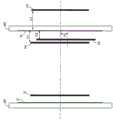
使用图1~2对本发明的实施方式1进行说明。首先,使用图1对本实施方式中的电力转换装置的结构进行说明。图1是示出本实施方式所涉及的电力转换装置的结构的一个例子的图。
本实施方式中的电力转换装置具有多个单位逆变器1。单位逆变器1具有无线送电部2、无线受电部3、DC/DC转换器部4、逆变器部5、控制部6、太阳光面板连接端子53、54(电力输入部)、变压器11、正极侧逆变器输出端子51以及负极侧逆变器输出端子52。The power conversion device in the present embodiment includes a plurality of
无线送电控制部2具有送电共振线圈31、送电线圈32、发送放大器39、振荡器38以及送电部电源41。DC/DC转换器部4具有开关MOS晶体管12a、12b、12c、12d、电容器18以及DC/DC控制部21。The wireless power transmission control unit 2 includes a power
逆变器部5具有逆变器MOS晶体管13a、13b、13c、13d(逆转换部)、链路电压平滑电容器14(平滑部)以及整流二极管15a、15b、15c、15d(正转换部)。无线受电部3具有受电共振线圈33、受电线圈34a、34b、34c、二极管桥35以及受电平滑电容器36。控制部6具有栅极控制电路37a、37b、37c。The
另外,在图1中,简化具有二极管桥35和受电平滑电容器36的受电电路,具有框图中记载的部分。In addition, in FIG. 1, the power reception circuit which has the
接下来,使用图2对图1中的结构的位置关系进行说明。图2是立体地示出本实施方式中的电力转换装置的构造的一个例子的图。在图2中,与图1所示的图中的编号相同的编号表示与图1相同的结构。无线送电部2、无线受电部3、DC/DC转换器部4以及逆变器部5安装在印刷电路基板上。Next, the positional relationship of the structure in FIG. 1 is demonstrated using FIG. 2. FIG. FIG. 2 is a perspective view showing an example of the structure of the power conversion device in the present embodiment. In FIG. 2 , the same reference numerals as those in the drawing shown in FIG. 1 indicate the same structures as those in FIG. 1 . The wireless power transmission unit 2 , the wireless power reception unit 3 , the DC/
无线送电部2设置为与无线受电部3分离并对置,使得能够向无线受电部3送电。The wireless power transmission unit 2 is provided so as to be separated from and opposed to the wireless power reception unit 3 so as to be able to transmit power to the wireless power reception unit 3 .
更详细而言,送电共振线圈31以及受电共振线圈33在印刷电路基板上由铜箔图案形成。此外,送电共振线圈31和受电共振线圈33配置为分离并对置,使得各自的线圈中心在同一轴上重叠。More specifically, the power
送电线圈32缠绕直径为1.0mm的铜线一圈并焊接到印刷电路基板上,线圈中心与送电共振线圈的中心轴重叠。受电线圈34a、34b、34c配置为经由受电共振线圈33接受的电力的大小大致相同。The
另外,铜线的直径不限于1.0mm,可以设为根据想传送的电力等来适当地变更。In addition, the diameter of the copper wire is not limited to 1.0 mm, and can be appropriately changed in accordance with the power to be transmitted and the like.
接下来,使用图1对本实施方式的各结构进行说明。在图1中,太阳光面板输出的DC电压经由太阳光面板连接端子53、54输入到DC/DC转换器部4。输入到DC/DC转换器部4的DC电压由被DC/DC控制部21控制的开关MOS晶体管12a~12d进行电压转换,并输出到变压器11。Next, each configuration of the present embodiment will be described with reference to FIG. 1 . In FIG. 1 , the DC voltage output by the solar panel is input to the DC/
从DC/DC转换器部2输出的DC电压由变压器11升压,并输入到逆变器部5的正转换部。正转换部对输入的DC电压进行正转换并输出到平滑部。平滑部对由正转换部进行了正转换的DC电压进行平滑,并将链路电压Vdc输出到逆转换部。The DC voltage output from the DC/DC converter unit 2 is boosted by the
另外,变压器11具有逆变器输出电压和DC/DC转换器部4的GND电位之间的耐电压。In addition, the
栅极控制电路37a~37c(控制部)对逆变器MOS晶体管13a~13c的栅极进行PWM控制。正转换部通过进行了PWM控制的逆变器MOS晶体管13a~13c的开关对链路电压Vdc进行转换,并输出商用的交流电力。The
振荡器38将以送电共振线圈31和受电共振线圈33的电磁场共振频率Fr振荡的电力输出到发送放大器39。发送放大器39放大所输入的电力并输出到送电线圈32。这些要通过独立于DC/DC转换器部4的不同的系统的送电部电源41来接受供电。The
通过送电共振线圈31和受电共振线圈33电磁耦合,从送电线圈32输出的电磁场(电力)传送到受电线圈34a、34b、34c。接受的电磁场由具有二极管桥35和受电平滑电容器36的受电电路平滑为直流电压,并成为栅极控制电路37a、37b、37c(控制部6)的电源电压。The electromagnetic field (electric power) output from the
由此,即使DC/DC转换器部4发生故障,也能够从无线送电部2向控制部6继续供给电力,因此能够防止正转换部的逆变器MOS晶体管13a~d的驱动控制变得不稳定。因此,能够防止逆变器MOS晶体管13a~d的短路。Thereby, even if the DC/
关于这一点,与以往技术进行对比,在以往,因为将从DC/DC转换器部经由变压器供给的电力用于正转换部的开关元件的驱动控制,所以在DC/DC转换器部发生故障的情况下,对正转换部的开关元件的驱动控制的电力供给也停止,且开关元件的开关工作变得不稳定,可能发生短路。In this regard, in contrast to the prior art, conventionally, since the electric power supplied from the DC/DC converter unit via the transformer was used for driving control of the switching elements of the positive conversion unit, a failure occurred in the DC/DC converter unit. In this case, the power supply to the driving control of the switching elements of the positive conversion unit is also stopped, the switching operation of the switching elements becomes unstable, and a short circuit may occur.
对此,在本实施方式中,通过将对控制部6的电力系统设为与DC/DC转换器部4的电力供给系统不同,从而即使在DC/DC转换器部4故障时,也预防了逆变器MOS晶体管的短路。In contrast, in the present embodiment, by setting the power system for the control unit 6 to be different from the power supply system for the DC/
此外,在DC/DC转换器部4和逆变器部5之间,需要与逆变器输出电压一致的绝缘耐电压。例如,在电力公司的三相系统电压中,要求6.6kV作为绝缘耐电压。在这种情况下,若在DC/DC转换器部4和逆变器部5之间确保11.0mm以上的空间,则能够绝缘。In addition, between the DC/
对此,如以往那样,在从DC/DC转换器部经由变压器供给用于正转换部的开关元件的驱动控制的电力的情况下,为了确保变压器中的耐压,需要大型化变压器。此外,即使在将该用于驱动控制的电力的供给源设为与来自DC/DC转换器部的供给不同的系统的情况下,也难以确保用于担保高耐压的绝缘性。On the other hand, when the electric power for driving and controlling the switching elements of the positive conversion unit is supplied from the DC/DC converter unit through the transformer as in the past, in order to ensure the withstand voltage in the transformer, the transformer needs to be enlarged in size. In addition, even when the power supply source for the drive control is a different system from the supply from the DC/DC converter unit, it is difficult to secure insulation for securing a high withstand voltage.
与此相对,在本实施方式中,如图2所示,在送电线圈32和受电线圈34a、34b之间,分离开基板间距离(例如60mm),能够确保具有6.6kV的绝缘耐压的绝缘性。On the other hand, in the present embodiment, as shown in FIG. 2 , between the
以上,根据本实施方式,即使DC/DC转换器部4的开关MOS晶体管12a~12d、DC/DC控制部21发生故障,在变压器11的次级侧不再产生电流,或者在逆变器部5不再产生链路电压Vdc,也能够通过不同的电源即送电部电源41,来维持栅极控制电路37a~37c的电源电压,并控制逆变器MOS13a~13d从而停止正极侧逆变器输出端子51和负极侧逆变器输出端子52间的输出。As described above, according to the present embodiment, even if the switching
此外,在逆变器MOS晶体管13a和逆变器MOS晶体管13c之间、以及逆变器MOS晶体管13a和逆变器MOS晶体管13b之间,需要与逆变器输出端子51和52间的电压一致的绝缘耐压,而在本实施方式中,通过分别将受电线圈34a和34b、以及34b和34c之间分离开并用空气绝缘,也能够确保该绝缘耐压。In addition, between the
另外,用分为送受电用线圈和共振线圈的结构对电力传送进行了说明,也可以使用通过串联谐振或者并列谐振而电磁场耦合的送电侧线圈和受电侧线圈。In addition, the power transmission has been described with a configuration divided into a power transmission and reception coil and a resonance coil, but a power transmission side coil and a power reception side coil which are electromagnetically coupled by series resonance or parallel resonance may be used.
此外,在本实施方式中,说明了受电线圈为三个的情况,但不限于三个。也可以通过在控制部侧共享受电线圈,将受电线圈的数量设为一个或者两个。也可以根据控制的逆变器MOS晶体管的数量,变更受电线圈的数量。In addition, in this embodiment, although the case where there are three power receiving coils was demonstrated, it is not limited to three. By sharing the power receiving coil on the control unit side, the number of the power receiving coils may be one or two. The number of power receiving coils may be changed according to the number of inverter MOS transistors to be controlled.
此外,在说明中,叙述了接受的电磁场成为栅极控制电路37a、37b、37c的电源电压,但也可以向其他的未图示的电压传感器、电流传感器、微处理器等供给电源。In the description, the received electromagnetic field is described as the power supply voltage of the
以上,在本实施方式的电力转换装置中,能够确保绝缘耐性,并且防止短路。As described above, in the power conversion device of the present embodiment, it is possible to prevent short circuits while ensuring insulation resistance.
[第二实施方式][Second Embodiment]
接下来,使用图3对本实施方式中的电力转换装置进行说明。本实施方式涉及串联连接多个第一实施方式中的单位逆变器1而获得的多路逆变器7。图3是示出本实施方式所涉及的多路逆变器7的结构例的图。对于说明与第一实施方式中的电力转换装置重复的部分,省略说明。Next, the power conversion device in this embodiment will be described with reference to FIG. 3 . The present embodiment relates to a multi-channel inverter 7 obtained by connecting a plurality of
多路逆变器7具有多个单位逆变器1、中央控制装置300、U相输出端子55、V相输出端子56以及W相输出端子57。The multiplex inverter 7 includes a plurality of
单位逆变器1的负极侧输出端子52与另外的单位逆变器的正极侧输出端子连接。通过将该连接多级串联,能够将单位逆变器输出电压±Vdc变为N倍并输出到U相输出端子55。The negative side output terminal 52 of the
例如,若所需的U相输出电压设为6.6kV,串联级数N设为8级,则为Vdc=6600÷2÷8=412.5V。因此,单位逆变器1的输出为±412.5V,并可获得6.6kV的多路逆变器输出。For example, if the required U-phase output voltage is set to 6.6kV, and the number of series series N is set to 8, then Vdc=6600÷2÷8=412.5V. Therefore, the output of the
另外,这对于V相和W相也是一样的,因此省略说明。In addition, this is the same for the V-phase and the W-phase, so the description is omitted.
在本实施方式中,将各个单位逆变器1串联连接,所述单位逆变器1具有包括送电共振线圈31等的无线送电部和包括受电共振线圈33等的无线受电部。中央控制装置300进行控制,控制各单位逆变器内的DC/DC控制部,使得各正极侧输出端子51和负极侧输出端子52间的输出电压的和即U相输出成为正弦波。In the present embodiment, the
除了内置该串联连接逆变器之外,多路逆变器7还内置V相、W相,中央控制装置300进行控制,以将三相交流输出到U相输出端子55、V相输出端子56、W相输出端子57。In addition to the built-in series-connected inverter, the multi-channel inverter 7 also has a built-in V-phase and a W-phase, and the
通过这样使具有多个单位逆变器1的多路逆变器7工作,能够确保DC/DC转换器部4和逆变器部5的绝缘耐压为6.6kV以上,并且确保逆变器MOS晶体管13a、13b、13c间的绝缘耐压为412.5V以上。此外,在DC/DC转换器部4故障时,能够控制正极侧输出端子51和负极侧输出端子52的输出,使U相输出端子55、V相输出端子56、W相输出端子57的各输出稳定地停止。By operating the multi-channel inverter 7 including the plurality of
以上,根据本实施方式,能够提供一种能够确保绝缘耐性并且防止短路的多路逆变器7。As described above, according to the present embodiment, it is possible to provide the multiplex inverter 7 that can prevent short circuits while ensuring insulation resistance.
[第三实施方式][Third Embodiment]
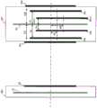
使用图4对本实施方式进行说明。图4是示出本实施方式所涉及的多路逆变器7的结构例的图。在本实施方式的说明中,省略与之前的说明重复的部分。This embodiment will be described with reference to FIG. 4 . FIG. 4 is a diagram showing a configuration example of the multi-channel inverter 7 according to the present embodiment. In the description of the present embodiment, parts overlapping with the previous description are omitted.
若叙述与图3的不同点,则多路逆变器7具有内置无线受电部3但却没有内置无线送电部2的单位逆变器44。If the difference from FIG. 3 is described, the multi-inverter 7 has a unit inverter 44 which has a built-in wireless power receiving unit 3 but does not have a built-in wireless power transmitting unit 2 .
图5示出了本实施方式所涉及的多路逆变器7的立体构造的结构例。在图5中,多路逆变器具有:多路逆变器架45;具有无线送电部和无线受电部这两者的单位逆变器1、101;以及仅具有无线受电部3的单位逆变器44、46、47。各无线受电部3的受电共振线圈33配置在多路逆变器架45中,使得其中心与其他的单位逆变器的受电共振线圈的中心同一轴。送电共振线圈31配置在多路逆变器架45中,以与要进行送电的无线受电部的受电共振线圈的中心同一轴。FIG. 5 shows a configuration example of the three-dimensional structure of the multi-channel inverter 7 according to the present embodiment. In FIG. 5 , the multi-inverter includes: the
另外,在此所说的同一轴不仅包括完全在同一轴上,还包括在同一轴的附近。此外,例如,若将效率最好的送电(受电)效率设为100%,则附近意味着只要在送电(受电)效率为95%左右的范围内即可。然而,该95%仅是一个例子,可以根据所需的送电(受电)效率适当地变更。In addition, the same axis referred to here includes not only the complete same axis, but also the vicinity of the same axis. In addition, for example, if the most efficient power transmission (power reception) efficiency is 100%, the vicinity means that the power transmission (power reception) efficiency is within a range of about 95%. However, this 95% is only an example, and can be appropriately changed according to the required power transmission (power reception) efficiency.
单位逆变器1的无线送电部2输出的频率F1的电磁波到达相邻的单位逆变器44的无线受电部3的受电共振线圈33,并将电力传送到单位逆变器44的无线受电部3。由无线受电部3接受的电力被整流并成为栅极控制部电源电压。The electromagnetic wave of the frequency F1 output by the wireless power transmission unit 2 of the
对此,单位逆变器101的无线送电部42输出的频率F2的电磁波到达相邻的单位逆变器47的无线受电部3并从中通过,进而到达相邻的单位逆变器44的受电共振线圈33。由此,单位逆变器44的无线受电部3接受电力,且接受的电力被整流并成为栅极控制部电源电压。In contrast, the electromagnetic wave of frequency F2 output from the wireless power transmission unit 42 of the unit inverter 101 reaches and passes through the wireless power reception unit 3 of the adjacent unit inverter 47 , and then reaches the adjacent unit inverter 44 . Power receiving
这样,单位逆变器44在自己的DC/DC转换器部4不具有无线送电部2,而从其他的单位逆变器接受频率F1和频率F2的电力,并使栅极控制部工作。In this way, the unit inverter 44 does not have the wireless power transmission unit 2 in its own DC/
由此,例如,在图5的结构中,通过具有无线送电部2的两台单位逆变器,五台单位逆变器能够工作,具有由部件数量削减带来的低成本化的效果。Thus, for example, in the configuration of FIG. 5 , five unit inverters can be operated by two unit inverters including the wireless power transmission unit 2 , and there is an effect of cost reduction due to reduction in the number of components.
另外,具有无线送电部2和无线受电部3的单位逆变器与仅具有无线受电部3的单位逆变器的比率不限于上述例子。能够根据来自无线送电部2的送电电力的大小、无线送电部2和无线受电部3的位置关系来适当地变更该比率。In addition, the ratio of the unit inverter including the wireless power transmission unit 2 and the wireless power reception unit 3 to the unit inverter including only the wireless power reception unit 3 is not limited to the above example. This ratio can be appropriately changed according to the magnitude of the power to be transmitted from the wireless power transmission unit 2 and the positional relationship between the wireless power transmission unit 2 and the wireless power reception unit 3 .
此外,中央控制装置300进行控制,使得无线送电部2能够向各个无线受电部3供给大致相同的电力。由此,例如,在从两个无线送电部2接受电力的无线受电部3的情况下,即使来自一个无线送电部2的送电输出变弱,也能够提高另一个无线送电部2的送电输出,因此无线受电部3能够接受稳定的电力供给。Further, the
此外,在上述的例子中,单位逆变器1送电的频率F1和单位逆变器101送电的频率F2是相同的频率。但是,即使频率F1和频率F2不同,也是本发明的一个实施例。In addition, in the above-mentioned example, the frequency F1 of the power transmission of the
以上,根据本实施方式,能够提供一种能够确保绝缘耐性并且防止短路、且低成本的多路逆变器。As described above, according to the present embodiment, it is possible to provide a low-cost multi-channel inverter capable of ensuring insulation resistance and preventing short circuits.
[第四实施方式][Fourth Embodiment]
使用图6对本实施方式中的单位逆变器进行说明。图6是示出本实施方式所涉及的单位逆变器的结构例的图。在本实施方式的说明中,省略与之前的说明重复的部分。The unit inverter in this embodiment will be described with reference to FIG. 6 . FIG. 6 is a diagram showing a configuration example of the unit inverter according to the present embodiment. In the description of the present embodiment, parts overlapping with the previous description are omitted.
若叙述与图1的不同点,则本实施方式中的单位逆变器601具有PWM数据生成部61、调制电路62、解调电路63以及PWM波形生成部64(控制信号输出部)。解调电路63与受电线圈34a、34b、34c的任意一个连接。1 , the unit inverter 601 in this embodiment includes a PWM data generation unit 61, a modulation circuit 62, a
在本实施方式中,设为通过PWM(脉冲宽度调制)控制逆变器部5的逆变器MOS晶体管13a~d并输出正弦波。In the present embodiment, the
在图6中,PWM数据生成部61计算要施加到逆变器MOS晶体管13a~13d的栅极的PWM波形的占空比并作为占空比数据(控制信号)输出。调制电路62基于PWM数据生成部61输出的占空比数据,对从振荡器38输出的电力传送波进行MSK调制。In FIG. 6 , the PWM data generating section 61 calculates the duty ratio of the PWM waveform to be applied to the gates of the
另外,该调制方法不限于MSK,除了MSK之外,可以是FSK、QPSK、QAM等数字调制。In addition, the modulation method is not limited to MSK, and may be digital modulation such as FSK, QPSK, and QAM in addition to MSK.
送电线圈32经由送电共振线圈31将调制的电力传送波传送到受电线圈34a~c。由受电线圈34c接收并调制的电力传送波被输入到解调电路63并进行MSK解调。被解调了的占空比数据由PWM波形生成部64转换为施加到逆变器MOS晶体管13a~13d的栅极的PWM波形并输出到各个栅极控制电路37a~c。栅极控制电路37a~c基于输入的PWM波形,驱动控制逆变器MOS晶体管13a~13d。The
通过这样工作,能够利用基于无线的电力传送电路来传送用于控制逆变器MOS晶体管13a~13d的占空比数据。由此,不再需要以往为了将占空比数据传送到栅极控制电路而使用的高耐电压光电耦合器、光纤,从而能够达到单位逆变器的低成本化。By operating in this way, the duty ratio data for controlling the
以上,根据本实施方式,能够提供一种在能够维持单位逆变器的绝缘耐性并且防止短路的基础上,进一步低成本的单位逆变器。As described above, according to the present embodiment, it is possible to provide a low-cost unit inverter while maintaining the insulation resistance of the unit inverter and preventing short circuits.
[第五的实施方式][Fifth Embodiment]
使用图7对本实施方式中的单位逆变器1的无线送受电系统进行说明。图7是示出实施方式所涉及的无线送受电系统的线圈的位置关系的一个例子的图。The wireless power transmission and reception system of the
在图7中,送电共振线圈31设置在搭载有DC/DC转换器部4的印刷基板400的面中的、搭载了逆变器部5的印刷基板500侧的面上。此外,受电共振线圈33设置在搭载了逆变器部的印刷基板500的面中的、搭载了DC/DC转换器部4的印刷基板400侧的面上。送电共振线圈31以及受电共振线圈33通过印刷基板的铜箔布线形成。In FIG. 7 , the power
送电线圈32和受电线圈34a、b在印刷基板400和印刷基板500之间分离设置。受电线圈34c设置在与受电线圈a、b的相反侧。受电线圈34a~c分别是一圈线圈,且用焊接等固定于印刷基板400、500,将接受的电力供给到各逆变器MOS晶体管13a~c的栅极控制电路37a~c。The
在此,为了进行各逆变器晶体管13a~c的栅极控制,在从一个送电线圈通过多个受电线圈分别向各个电路供给电力的情况下,优选各受电线圈的受电量几乎相等。Here, in order to perform gate control of each of the
与此相对,在本实施方式的无线送受电系统中,送电共振线圈31以及受电共振线圈33的中心配置为大致同一轴(以下,称为中心轴)。此外,受电线圈34a配置在与中心轴大致同一轴上,且与受电共振线圈33分离开距离h1。对此,受电线圈34b配置为其中心从中心轴偏移距离d1,且与受电共振线圈33分离开距离h2。此外,受电线圈34c配置在与中心轴大致同一轴上,且与受电共振线圈分离开距离h3。On the other hand, in the wireless power transmission and reception system of the present embodiment, the centers of the power
这些距离处于h2<h1<h3的关系。These distances are in the relationship of h2<h1<h3.
与受电共振线圈的距离越近,受电线圈34a~c的受电量越大。此外,在受电线圈34b中,受电量减少中心轴偏移的量。因此,分离得最远的距离为h3的受电线圈34c的受电量最小。受电线圈34a比受电线圈34c更靠近受电共振线圈33,因此其受电量通常比受电线圈34c的受电量大。The closer the distance to the power receiving resonance coil, the greater the amount of power received by the power receiving coils 34a to c. In addition, in the
如果最靠近受电共振线圈33的受电线圈34b配置在与中心轴的同一轴上,则其受电量最大。但是,在本实施方式中,受电线圈34b配置为从中心轴上偏离d1,因此受电量减少该偏移量。此外,虽然受电线圈34a比h3更靠近受电共振线圈,但因为受到受电线圈34b的影响,所以受电量减少。When the
因此,如果进行将受电线圈34a、b的配置从同一轴上偏移,或者,配置在受电线圈34a、b相互影响的位置等设计来调整受电量,使得与最少受电量的受电线圈34c的受电量大致相同,则能够将受电线圈34a~c的受电量设为大致相同。Therefore, if the power receiving coils 34a and b are arranged to be shifted from the same axis, or the power receiving coils 34a and b are arranged at positions where the power receiving coils 34a and b interact with each other, the power reception amount can be adjusted so that the
另外,在以上的说明中,为了简化说明,对除了受电线圈34b之外的线圈在同一轴上进行了说明。但是,不限于此。本实施方式中的意图在于,在多个受电线圈与一个送电线圈对置并依次排列配置的情况下,考虑到与受电共振线圈的距离、从中心轴的偏移、受电线圈彼此的影响等,分别进行配置,使得各受电线圈的受电量大致相同。In addition, in the above description, in order to simplify the description, the coils other than the
[第六实施方式][Sixth Embodiment]
使用图8对本实施方式中的单位逆变器1的无线送受电系统进行说明。图8是示出本实施方式所涉及的无线送受电系统的线圈的位置关系的一个例子的图。The wireless power transmission and reception system of the
在图8中,若叙述与图7的不同点,则送电线圈32和受电线圈34a、b在印刷基板401和印刷基板501之间分离设置。受电线圈34c、d设置在与受电线圈a、b的相反侧。In FIG. 8 , the difference from FIG. 7 is described, the
送电线圈32是由印刷基板401的铜箔布线形成的一圈的线圈,受电线圈34a~d分别是由印刷基板501的铜箔布线形成的一圈的线圈。在此,与第五实施例一样,各受电线圈的受电量优选为相等。The
与此相对,在本实施方式中的单位逆变器1的无线送受电系统中,送电共振线圈31以及受电共振线圈33的中心配置为在大致同一轴(以下,称为中心轴)上。此外,受电线圈34a、34d配置在与中心轴大致同一轴上,且与受电共振线圈33分离开距离h1、h4。On the other hand, in the wireless power transmission and reception system of the
对此,受电线圈34b的中心与受电线圈34c的中心轴一致,且形成一对线圈对。而且,线圈对的中心配置为从受电共振线圈的中心轴偏移距离d1,且分别与受电共振线圈33分离开距离h2、h3。这些距离处于h2、h3<h1、h4的关系。On the other hand, the center of the
为了均衡受电线圈34a~d的受电量,能够通过对线圈对的距离h2和距离h3进行微调整,并且对线圈对的距离h1和h4进行微调整来实现。也就是说,通过使线圈对的中心轴一致来配置,从而受电线圈34a~d的受电量能够仅由h1、h2、h3、h4确定。In order to balance the power reception amount of the power receiving coils 34a to d, it can be realized by finely adjusting the distances h2 and h3 of the coil pair, and finely adjusting the distances h1 and h4 of the coil pair. That is, by arranging the center axes of the coil pairs to coincide, the received amounts of the power receiving coils 34a to d can be determined only by h1, h2, h3, and h4.
以上,根据本实施方式,通过偏移两组线圈对的中心轴,仅调整各线圈对离受电共振线圈33的距离,就能够将各线圈的受电量调整为大致相同。As described above, according to the present embodiment, by offsetting the central axes of the two coil pairs and adjusting the distance between each coil pair and the power
[第七实施方式][Seventh Embodiment]
使用图9对本实施方式中的单位逆变器1的无线送受电系统进行说明。图9是示出本实施方式所涉及的无线送受电系统的线圈的位置关系的一个例子的图。The wireless power transmission and reception system of the
在本实施方式所涉及的无线送受电系统中,是在受电线圈数量为4的第六实施方式的例子中,将受电线圈的数量概括为n+1的结构。若叙述与图8的不同点,则受电线圈34n配置在送电共振线圈31和受电共振线圈33之间,且受电线圈34n+1设置在与受电线圈34a、34b、34n的相反侧。In the wireless power transmission and reception system according to the present embodiment, in the example of the sixth embodiment in which the number of power reception coils is four, the number of power reception coils is summarized as n+1. 8, the
受电线圈34n的中心配置在受电线圈34n+1的中心轴上,且形成一对线圈对。而且,该线圈对的中心配置为从受电共振线圈的中心轴偏移距离dN(>dn-1),且分别与受电共振线圈33分离开距离hn、hn+1。The center of the
这些距离处于d1<dn-1<dN以及hn、hn+1<hn-1,hn-2<h2、h3<h1、h4的关系。These distances are in the relationship of d1<dn-1<dN and hn, hn+1<hn-1, hn-2<h2, h3<h1, and h4.
为了均衡受电线圈34a~n+1的受电量,能够通过对线圈对的距离hn和距离hn+1进行微调整,对线圈对的距离h2和距离h3进行微调整,并且对线圈对的距离h1和h4进行微调整来实现。In order to balance the amount of power received by the power receiving coils 34a to n+1, by finely adjusting the distance hn and the distance hn+1 of the coil pair, the distance h2 and the distance h3 of the coil pair can be finely adjusted, and the distance of the coil pair can be finely adjusted. H1 and h4 are fine-tuned to achieve this.
也就是说,通过使线圈对的中心轴一致来配置,从而受电线圈34a~n+1的受电量能够仅由h1、h2、h3、h4、hn、hn+1确定。That is, by arranging the center axes of the coil pairs to coincide, the received amounts of the power receiving coils 34a to n+1 can be determined only by h1, h2, h3, h4, hn, and hn+1.
以上,根据本实施方式,能够从一个送电线圈向多个受电线圈传送大致相同的电力。As described above, according to the present embodiment, substantially the same electric power can be transmitted from one power transmission coil to a plurality of power reception coils.
另外,本发明不限于上述实施方式,且包含各种变形例。例如,为了以易于理解的方式说明本发明,已经详细说明了上述实施分解方式,且不必限于具备说明的全部的结构的实施分解方式。此外,能够将某个实施方式的结构的一部分置换为其他的实施方式的结构,也能够将其他的实施方式的结构添加到某个实施方式的结构中。此外,能够针对各实施方式的结构的一部分进行其他的结构的追加/削除/置换。In addition, the present invention is not limited to the above-described embodiment, and includes various modifications. For example, in order to explain the present invention in an easy-to-understand manner, the above-described disassembled embodiment has been described in detail, and is not necessarily limited to the disassembled embodiment having all the structures described. Moreover, a part of the structure of a certain embodiment can be replaced with the structure of another embodiment, and the structure of another embodiment can also be added to the structure of a certain embodiment. In addition, addition/deletion/replacement of other structures can be performed with respect to a part of the structures of each embodiment.
此外,关于上述各结构、功能、处理部、处理装置等,可以通过用例如集成电路设计等来硬件实现其一部分或者全部。此外,上述各结构、功能等也可以通过处理器解释、执行实现各个功能的程序而利用软件来实现。实现各功能的程序、表格、文件等信息能够存储在存储器、硬盘、SSD(Solid State Drive,固态驱动器)等记录装置或者IC卡、SD卡、DVD等记录介质中。In addition, regarding each of the above-described structures, functions, processing units, processing devices, and the like, a part or all of them can be realized in hardware by, for example, an integrated circuit design or the like. In addition, each of the above-described structures, functions, and the like can also be realized by software when a processor interprets and executes a program that realizes each function. Information such as programs, tables, and files for realizing each function can be stored in a recording device such as a memory, a hard disk, and an SSD (Solid State Drive), or a recording medium such as an IC card, SD card, and DVD.
此外,示出了在说明方面认为是有必要的控制线、信息线,但在产品方面,不一定示出全部的控制线、信息线。实际上也可以考虑几乎全部的结构都相互连接。In addition, control lines and information lines that are considered necessary for description are shown, but not all control lines and information lines are necessarily shown in terms of products. In practice it is also conceivable that almost all structures are interconnected.
附图标记说明Description of reference numerals
1:单位逆变器1: Unit inverter
2:无线送电部2: Wireless Power Transmission Department
3:无线受电部3: Wireless Power Receiving Unit
4:DC/DC转换器部4: DC/DC converter section
5:逆变器部5: Inverter part
7:多路逆变器7: Multi-channel inverter
53、54:太阳光面板连接端子53, 54: Solar panel connection terminals
11:变压器11: Transformer
12a、12b、12c、12d:开关MOS晶体管12a, 12b, 12c, 12d: switching MOS transistors
18:电容器18: Capacitor
13a、13b、13c、13d:逆变器MOS晶体管13a, 13b, 13c, 13d: Inverter MOS transistors
14:链路电压平滑电容器14: Link voltage smoothing capacitor
15a、15b、15c、15d:整流二极管15a, 15b, 15c, 15d: Rectifier diodes
51:正极侧逆变器输出端子51: Positive side inverter output terminal
52:负极侧逆变器输出端子52: Negative side inverter output terminal
21:DC/DC转换器控制部21: DC/DC converter control section
31:送电共振线圈31: Power transmission resonance coil
32:送电线圈32: Power transmission coil
39:发送放大器39: Transmit Amplifier
38:振荡器38: Oscillator
41:送电部电源41: Power supply of the power transmission department
33:受电共振线圈33: Power receiving resonance coil
34a、34b、34c:受电线圈34a, 34b, 34c: Power receiving coils
35:二极管桥35: Diode Bridge
36:受电平滑电容器36: Power-receiving smoothing capacitor
37a、37b、37c:栅极控制电路37a, 37b, 37c: gate control circuit
Claims (11)
Translated fromChineseApplications Claiming Priority (1)
| Application Number | Priority Date | Filing Date | Title |
|---|---|---|---|
| PCT/JP2016/061192WO2017175319A1 (en) | 2016-04-06 | 2016-04-06 | Wireless power transmission and reception system, power conversion apparatus provided with same, and power conversion method |
Publications (2)
| Publication Number | Publication Date |
|---|---|
| CN109121455A CN109121455A (en) | 2019-01-01 |
| CN109121455Btrue CN109121455B (en) | 2020-12-15 |
Family
ID=60000914
Family Applications (1)
| Application Number | Title | Priority Date | Filing Date |
|---|---|---|---|
| CN201680083975.2AActiveCN109121455B (en) | 2016-04-06 | 2016-04-06 | Power conversion device and power conversion method |
Country Status (5)
| Country | Link |
|---|---|
| US (1) | US11018528B2 (en) |
| EP (1) | EP3442107A4 (en) |
| JP (1) | JP6253808B1 (en) |
| CN (1) | CN109121455B (en) |
| WO (1) | WO2017175319A1 (en) |
Families Citing this family (4)
| Publication number | Priority date | Publication date | Assignee | Title |
|---|---|---|---|---|
| AU2017357919B2 (en)* | 2016-11-09 | 2024-05-02 | Sigma Genetics, Inc. | Systems, devices, and methods for electroporation induced by magnetic fields |
| JP7069913B2 (en)* | 2018-03-22 | 2022-05-18 | Tdk株式会社 | Coil unit, wireless power transmission device, wireless power receiving device, and wireless power transmission system |
| TWI729707B (en)* | 2020-02-18 | 2021-06-01 | 國立虎尾科技大學 | Wireless power transferring system |
| JP7476964B2 (en)* | 2020-06-30 | 2024-05-01 | 株式会社村田製作所 | Wireless Power Supply System |
Citations (3)
| Publication number | Priority date | Publication date | Assignee | Title |
|---|---|---|---|---|
| CN102037526A (en)* | 2008-05-22 | 2011-04-27 | 三菱电机株式会社 | Electronic device and method for connecting electronic circuit board |
| CN203871929U (en)* | 2014-03-14 | 2014-10-08 | 东芝泰格有限公司 | Power transmission apparatus, power supplying apparatus, power receiving apparatus and coil apparatus |
| CN104285358A (en)* | 2012-05-14 | 2015-01-14 | 日立化成株式会社 | Antenna board for non-contact charging device and charging device using the antenna board |
Family Cites Families (24)
| Publication number | Priority date | Publication date | Assignee | Title |
|---|---|---|---|---|
| JP2004342325A (en) | 2003-05-12 | 2004-12-02 | Matsushita Electric Works Ltd | Discharge lamp lighting device |
| JP2007151224A (en) | 2005-11-24 | 2007-06-14 | Shindengen Electric Mfg Co Ltd | Inverter power unit |
| US20090093687A1 (en) | 2007-03-08 | 2009-04-09 | Telfort Valery G | Systems and methods for determining a physiological condition using an acoustic monitor |
| JP4924499B2 (en)* | 2008-03-19 | 2012-04-25 | Tdk株式会社 | Switching power supply |
| CN101261764A (en)* | 2008-04-24 | 2008-09-10 | 上海交通大学 | Wireless drive system for power switching devices |
| JP5164806B2 (en)* | 2008-11-12 | 2013-03-21 | サンデン株式会社 | Vehicle communication control device |
| JP5135204B2 (en) | 2008-12-26 | 2013-02-06 | 株式会社日立製作所 | Non-contact power transmission system and load device in the non-contact power transmission system |
| BRPI0924914A2 (en)* | 2009-05-14 | 2016-08-30 | Toyota Motor Co Ltd | contactless energy capture equipment and vehicle incorporating the same |
| JP5527407B2 (en) | 2010-04-30 | 2014-06-18 | 富士通株式会社 | Wireless power receiving apparatus and power receiving method |
| CN103370849B (en)* | 2011-02-15 | 2017-03-22 | 丰田自动车株式会社 | Non-contact power receiving apparatus, vehicle having the non-contact power receiving apparatus mounted therein, non-contact power supply equipment, method for controlling non-contact power receiving apparatus, and method for controlling non-contact |
| JP2012186949A (en)* | 2011-03-07 | 2012-09-27 | Hitachi Maxell Energy Ltd | Non-contact power transmission device utilizing magnetic field resonance |
| JP2012205379A (en) | 2011-03-25 | 2012-10-22 | Sanyo Electric Co Ltd | Charging system, power supply device, mobile body, wireless power transmission and reception system, and power reception device |
| CN103403957B (en)* | 2011-11-01 | 2016-03-02 | 松下电器产业株式会社 | Resonance coupler |
| JP6083648B2 (en)* | 2011-11-01 | 2017-02-22 | パナソニックIpマネジメント株式会社 | Gate drive circuit |
| US9263971B2 (en)* | 2011-12-16 | 2016-02-16 | Empower Micro Systems Inc. | Distributed voltage source inverters |
| JP6065375B2 (en)* | 2012-02-17 | 2017-01-25 | 富士電機株式会社 | Power converter and grid interconnection system using the same |
| JP5866506B2 (en)* | 2013-08-27 | 2016-02-17 | パナソニックIpマネジメント株式会社 | Gate drive circuit |
| JP5910595B2 (en)* | 2013-09-24 | 2016-04-27 | 株式会社デンソー | Isolated power supply |
| US9479073B2 (en)* | 2013-11-12 | 2016-10-25 | Futurewei Technologies, Inc. | Gate drive apparatus for resonant converters |
| US9705324B2 (en)* | 2013-12-03 | 2017-07-11 | Abb Schweiz Ag | Converter system for AC power sources |
| JP6213229B2 (en) | 2013-12-26 | 2017-10-18 | 株式会社明電舎 | Insulation structure of power converter |
| SG10201401850RA (en)* | 2014-04-25 | 2015-11-27 | Rockwell Automation Asia Pacific Business Ct Pte Ltd | Motor Drive Switched Mode Power Supply Systems And Methods |
| JP2017070047A (en)* | 2015-09-29 | 2017-04-06 | 株式会社日立製作所 | Power supply |
| CN105257564A (en) | 2015-10-16 | 2016-01-20 | 珠海格力电器股份有限公司 | Electric fan |
- 2016
- 2016-04-06CNCN201680083975.2Apatent/CN109121455B/enactiveActive
- 2016-04-06JPJP2016562600Apatent/JP6253808B1/enactiveActive
- 2016-04-06WOPCT/JP2016/061192patent/WO2017175319A1/ennot_activeCeased
- 2016-04-06EPEP16897878.1Apatent/EP3442107A4/ennot_activeWithdrawn
- 2016-04-06USUS16/090,538patent/US11018528B2/enactiveActive
Patent Citations (3)
| Publication number | Priority date | Publication date | Assignee | Title |
|---|---|---|---|---|
| CN102037526A (en)* | 2008-05-22 | 2011-04-27 | 三菱电机株式会社 | Electronic device and method for connecting electronic circuit board |
| CN104285358A (en)* | 2012-05-14 | 2015-01-14 | 日立化成株式会社 | Antenna board for non-contact charging device and charging device using the antenna board |
| CN203871929U (en)* | 2014-03-14 | 2014-10-08 | 东芝泰格有限公司 | Power transmission apparatus, power supplying apparatus, power receiving apparatus and coil apparatus |
Also Published As
| Publication number | Publication date |
|---|---|
| EP3442107A1 (en) | 2019-02-13 |
| CN109121455A (en) | 2019-01-01 |
| JP6253808B1 (en) | 2017-12-27 |
| WO2017175319A1 (en) | 2017-10-12 |
| JPWO2017175319A1 (en) | 2018-04-12 |
| EP3442107A4 (en) | 2019-12-04 |
| US20190115789A1 (en) | 2019-04-18 |
| US11018528B2 (en) | 2021-05-25 |
Similar Documents
| Publication | Publication Date | Title |
|---|---|---|
| CN109121455B (en) | Power conversion device and power conversion method | |
| US11427095B2 (en) | Wireless charging system | |
| US20180131242A1 (en) | Inductive power transmitter, receiver and method of operation | |
| CN103731036A (en) | Bidirectional DC/DC Converter | |
| CN111095767B (en) | Driving power supply device | |
| US8559194B2 (en) | Converter circuit and unit and system comprising such converter circuit | |
| JP5217324B2 (en) | Power supply system | |
| JP6844716B2 (en) | Inverter control board | |
| JP5716877B2 (en) | Power transmission system | |
| JP2018093691A (en) | Power feeding device and wireless power transmission device using the same | |
| JP5843299B1 (en) | Inverter drive | |
| CN111200373B (en) | Isolated network power supply for CT scanner | |
| JP2017063526A (en) | Contactless power transmission equipment | |
| US8406016B2 (en) | Power supply circuit and information processing apparatus for power factor correction and stable power supply | |
| JP6615385B2 (en) | Gate drive device | |
| US20090116264A1 (en) | Power supply circuit with voltage converting circuits and control method therefor | |
| US11799388B2 (en) | Drive system having a first converter and at least one second converter | |
| CN206452299U (en) | A kind of converter | |
| JP2017005841A (en) | Power transmission apparatus | |
| JP2023099964A (en) | motor drive system | |
| JP5416337B2 (en) | Electric motor control device | |
| JP2015100256A (en) | Non-contact power feeding device | |
| CN119173981A (en) | A power supply arrangement, a plasma generating device and a method for controlling multiple plasma processes | |
| JP2019115221A (en) | Power transmission device | |
| JP2007174518A (en) | Power system |
Legal Events
| Date | Code | Title | Description |
|---|---|---|---|
| PB01 | Publication | ||
| PB01 | Publication | ||
| SE01 | Entry into force of request for substantive examination | ||
| SE01 | Entry into force of request for substantive examination | ||
| GR01 | Patent grant | ||
| GR01 | Patent grant |