CN109121291B - Semiconductor device and method for constructing semiconductor device - Google Patents
Semiconductor device and method for constructing semiconductor deviceDownload PDFInfo
- Publication number
- CN109121291B CN109121291BCN201810613513.8ACN201810613513ACN109121291BCN 109121291 BCN109121291 BCN 109121291BCN 201810613513 ACN201810613513 ACN 201810613513ACN 109121291 BCN109121291 BCN 109121291B
- Authority
- CN
- China
- Prior art keywords
- circuit board
- printed circuit
- metal layers
- contact pads
- metal
- Prior art date
- Legal status (The legal status is an assumption and is not a legal conclusion. Google has not performed a legal analysis and makes no representation as to the accuracy of the status listed.)
- Active
Links
- 238000000034methodMethods0.000titleclaimsabstractdescription90
- 239000004065semiconductorSubstances0.000titleclaimsabstractdescription36
- 229910052751metalInorganic materials0.000claimsabstractdescription268
- 239000002184metalSubstances0.000claimsabstractdescription268
- 239000004020conductorSubstances0.000claimsabstractdescription53
- 238000005553drillingMethods0.000claimsabstractdescription20
- 230000008878couplingEffects0.000claimsdescription2
- 238000010168coupling processMethods0.000claimsdescription2
- 238000005859coupling reactionMethods0.000claimsdescription2
- 239000010410layerSubstances0.000description233
- 239000012792core layerSubstances0.000description30
- 238000004519manufacturing processMethods0.000description25
- 239000000758substrateSubstances0.000description8
- 239000012790adhesive layerSubstances0.000description5
- 229910000679solderInorganic materials0.000description5
- -1etc.)Substances0.000description4
- 239000000463materialSubstances0.000description4
- 238000005476solderingMethods0.000description4
- 238000009792diffusion processMethods0.000description3
- RYGMFSIKBFXOCR-UHFFFAOYSA-NCopperChemical compound[Cu]RYGMFSIKBFXOCR-UHFFFAOYSA-N0.000description2
- 239000004593EpoxySubstances0.000description2
- XUIMIQQOPSSXEZ-UHFFFAOYSA-NSiliconChemical compound[Si]XUIMIQQOPSSXEZ-UHFFFAOYSA-N0.000description2
- 150000001875compoundsChemical class0.000description2
- 229910052802copperInorganic materials0.000description2
- 239000010949copperSubstances0.000description2
- 230000005611electricityEffects0.000description2
- 239000011152fibreglassSubstances0.000description2
- 230000005669field effectEffects0.000description2
- 239000011810insulating materialSubstances0.000description2
- 238000000465mouldingMethods0.000description2
- 229920003207poly(ethylene-2,6-naphthalate)Polymers0.000description2
- 239000011112polyethylene naphthalateSubstances0.000description2
- 229920000139polyethylene terephthalatePolymers0.000description2
- 239000005020polyethylene terephthalateSubstances0.000description2
- 229920001343polytetrafluoroethylenePolymers0.000description2
- 239000004810polytetrafluoroethyleneSubstances0.000description2
- 229910052710siliconInorganic materials0.000description2
- 239000010703siliconSubstances0.000description2
- JYEUMXHLPRZUAT-UHFFFAOYSA-N1,2,3-triazineChemical compoundC1=CN=NN=C1JYEUMXHLPRZUAT-UHFFFAOYSA-N0.000description1
- XQUPVDVFXZDTLT-UHFFFAOYSA-N1-[4-[[4-(2,5-dioxopyrrol-1-yl)phenyl]methyl]phenyl]pyrrole-2,5-dioneChemical compoundO=C1C=CC(=O)N1C(C=C1)=CC=C1CC1=CC=C(N2C(C=CC2=O)=O)C=C1XQUPVDVFXZDTLT-UHFFFAOYSA-N0.000description1
- JMASRVWKEDWRBT-UHFFFAOYSA-NGallium nitrideChemical compound[Ga]#NJMASRVWKEDWRBT-UHFFFAOYSA-N0.000description1
- 239000003989dielectric materialSubstances0.000description1
- 239000003292glueSubstances0.000description1
- 238000010438heat treatmentMethods0.000description1
- 229910044991metal oxideInorganic materials0.000description1
- 150000004706metal oxidesChemical class0.000description1
- 238000001465metallisationMethods0.000description1
- 229920003192poly(bis maleimide)Polymers0.000description1
- 239000002356single layerSubstances0.000description1
- 238000005245sinteringMethods0.000description1
Images


Classifications
- H—ELECTRICITY
- H05—ELECTRIC TECHNIQUES NOT OTHERWISE PROVIDED FOR
- H05K—PRINTED CIRCUITS; CASINGS OR CONSTRUCTIONAL DETAILS OF ELECTRIC APPARATUS; MANUFACTURE OF ASSEMBLAGES OF ELECTRICAL COMPONENTS
- H05K3/00—Apparatus or processes for manufacturing printed circuits
- H05K3/0011—Working of insulating substrates or insulating layers
- H05K3/0017—Etching of the substrate by chemical or physical means
- H05K3/0026—Etching of the substrate by chemical or physical means by laser ablation
- H05K3/0032—Etching of the substrate by chemical or physical means by laser ablation of organic insulating material
- H05K3/0038—Etching of the substrate by chemical or physical means by laser ablation of organic insulating material combined with laser drilling through a metal layer
- H—ELECTRICITY
- H05—ELECTRIC TECHNIQUES NOT OTHERWISE PROVIDED FOR
- H05K—PRINTED CIRCUITS; CASINGS OR CONSTRUCTIONAL DETAILS OF ELECTRIC APPARATUS; MANUFACTURE OF ASSEMBLAGES OF ELECTRICAL COMPONENTS
- H05K1/00—Printed circuits
- H05K1/02—Details
- H05K1/14—Structural association of two or more printed circuits
- H05K1/142—Arrangements of planar printed circuit boards in the same plane, e.g. auxiliary printed circuit insert mounted in a main printed circuit
- H—ELECTRICITY
- H01—ELECTRIC ELEMENTS
- H01L—SEMICONDUCTOR DEVICES NOT COVERED BY CLASS H10
- H01L23/00—Details of semiconductor or other solid state devices
- H01L23/52—Arrangements for conducting electric current within the device in operation from one component to another, i.e. interconnections, e.g. wires, lead frames
- H01L23/538—Arrangements for conducting electric current within the device in operation from one component to another, i.e. interconnections, e.g. wires, lead frames the interconnection structure between a plurality of semiconductor chips being formed on, or in, insulating substrates
- H01L23/5389—Arrangements for conducting electric current within the device in operation from one component to another, i.e. interconnections, e.g. wires, lead frames the interconnection structure between a plurality of semiconductor chips being formed on, or in, insulating substrates the chips being integrally enclosed by the interconnect and support structures
- H—ELECTRICITY
- H01—ELECTRIC ELEMENTS
- H01L—SEMICONDUCTOR DEVICES NOT COVERED BY CLASS H10
- H01L24/00—Arrangements for connecting or disconnecting semiconductor or solid-state bodies; Methods or apparatus related thereto
- H01L24/01—Means for bonding being attached to, or being formed on, the surface to be connected, e.g. chip-to-package, die-attach, "first-level" interconnects; Manufacturing methods related thereto
- H01L24/18—High density interconnect [HDI] connectors; Manufacturing methods related thereto
- H01L24/19—Manufacturing methods of high density interconnect preforms
- H—ELECTRICITY
- H01—ELECTRIC ELEMENTS
- H01L—SEMICONDUCTOR DEVICES NOT COVERED BY CLASS H10
- H01L24/00—Arrangements for connecting or disconnecting semiconductor or solid-state bodies; Methods or apparatus related thereto
- H01L24/01—Means for bonding being attached to, or being formed on, the surface to be connected, e.g. chip-to-package, die-attach, "first-level" interconnects; Manufacturing methods related thereto
- H01L24/18—High density interconnect [HDI] connectors; Manufacturing methods related thereto
- H01L24/20—Structure, shape, material or disposition of high density interconnect preforms
- H—ELECTRICITY
- H05—ELECTRIC TECHNIQUES NOT OTHERWISE PROVIDED FOR
- H05K—PRINTED CIRCUITS; CASINGS OR CONSTRUCTIONAL DETAILS OF ELECTRIC APPARATUS; MANUFACTURE OF ASSEMBLAGES OF ELECTRICAL COMPONENTS
- H05K1/00—Printed circuits
- H05K1/02—Details
- H05K1/11—Printed elements for providing electric connections to or between printed circuits
- H05K1/111—Pads for surface mounting, e.g. lay-out
- H05K1/112—Pads for surface mounting, e.g. lay-out directly combined with via connections
- H05K1/113—Via provided in pad; Pad over filled via
- H—ELECTRICITY
- H05—ELECTRIC TECHNIQUES NOT OTHERWISE PROVIDED FOR
- H05K—PRINTED CIRCUITS; CASINGS OR CONSTRUCTIONAL DETAILS OF ELECTRIC APPARATUS; MANUFACTURE OF ASSEMBLAGES OF ELECTRICAL COMPONENTS
- H05K1/00—Printed circuits
- H05K1/18—Printed circuits structurally associated with non-printed electric components
- H05K1/182—Printed circuits structurally associated with non-printed electric components associated with components mounted in the printed circuit board, e.g. insert mounted components [IMC]
- H05K1/185—Components encapsulated in the insulating substrate of the printed circuit or incorporated in internal layers of a multilayer circuit
- H—ELECTRICITY
- H05—ELECTRIC TECHNIQUES NOT OTHERWISE PROVIDED FOR
- H05K—PRINTED CIRCUITS; CASINGS OR CONSTRUCTIONAL DETAILS OF ELECTRIC APPARATUS; MANUFACTURE OF ASSEMBLAGES OF ELECTRICAL COMPONENTS
- H05K3/00—Apparatus or processes for manufacturing printed circuits
- H05K3/0011—Working of insulating substrates or insulating layers
- H05K3/0044—Mechanical working of the substrate, e.g. drilling or punching
- H05K3/0047—Drilling of holes
- H—ELECTRICITY
- H05—ELECTRIC TECHNIQUES NOT OTHERWISE PROVIDED FOR
- H05K—PRINTED CIRCUITS; CASINGS OR CONSTRUCTIONAL DETAILS OF ELECTRIC APPARATUS; MANUFACTURE OF ASSEMBLAGES OF ELECTRICAL COMPONENTS
- H05K3/00—Apparatus or processes for manufacturing printed circuits
- H05K3/30—Assembling printed circuits with electric components, e.g. with resistor
- H05K3/32—Assembling printed circuits with electric components, e.g. with resistor electrically connecting electric components or wires to printed circuits
- H05K3/321—Assembling printed circuits with electric components, e.g. with resistor electrically connecting electric components or wires to printed circuits by conductive adhesives
- H—ELECTRICITY
- H05—ELECTRIC TECHNIQUES NOT OTHERWISE PROVIDED FOR
- H05K—PRINTED CIRCUITS; CASINGS OR CONSTRUCTIONAL DETAILS OF ELECTRIC APPARATUS; MANUFACTURE OF ASSEMBLAGES OF ELECTRICAL COMPONENTS
- H05K3/00—Apparatus or processes for manufacturing printed circuits
- H05K3/40—Forming printed elements for providing electric connections to or between printed circuits
- H05K3/4007—Surface contacts, e.g. bumps
- H—ELECTRICITY
- H05—ELECTRIC TECHNIQUES NOT OTHERWISE PROVIDED FOR
- H05K—PRINTED CIRCUITS; CASINGS OR CONSTRUCTIONAL DETAILS OF ELECTRIC APPARATUS; MANUFACTURE OF ASSEMBLAGES OF ELECTRICAL COMPONENTS
- H05K3/00—Apparatus or processes for manufacturing printed circuits
- H05K3/46—Manufacturing multilayer circuits
- H05K3/4688—Composite multilayer circuits, i.e. comprising insulating layers having different properties
- H05K3/4694—Partitioned multilayer circuits having adjacent regions with different properties, e.g. by adding or inserting locally circuit layers having a higher circuit density
- H—ELECTRICITY
- H05—ELECTRIC TECHNIQUES NOT OTHERWISE PROVIDED FOR
- H05K—PRINTED CIRCUITS; CASINGS OR CONSTRUCTIONAL DETAILS OF ELECTRIC APPARATUS; MANUFACTURE OF ASSEMBLAGES OF ELECTRICAL COMPONENTS
- H05K2201/00—Indexing scheme relating to printed circuits covered by H05K1/00
- H05K2201/09—Shape and layout
- H05K2201/09209—Shape and layout details of conductors
- H05K2201/095—Conductive through-holes or vias
- H05K2201/09536—Buried plated through-holes, i.e. plated through-holes formed in a core before lamination
- H—ELECTRICITY
- H05—ELECTRIC TECHNIQUES NOT OTHERWISE PROVIDED FOR
- H05K—PRINTED CIRCUITS; CASINGS OR CONSTRUCTIONAL DETAILS OF ELECTRIC APPARATUS; MANUFACTURE OF ASSEMBLAGES OF ELECTRICAL COMPONENTS
- H05K2201/00—Indexing scheme relating to printed circuits covered by H05K1/00
- H05K2201/09—Shape and layout
- H05K2201/09209—Shape and layout details of conductors
- H05K2201/095—Conductive through-holes or vias
- H05K2201/09563—Metal filled via
- H—ELECTRICITY
- H05—ELECTRIC TECHNIQUES NOT OTHERWISE PROVIDED FOR
- H05K—PRINTED CIRCUITS; CASINGS OR CONSTRUCTIONAL DETAILS OF ELECTRIC APPARATUS; MANUFACTURE OF ASSEMBLAGES OF ELECTRICAL COMPONENTS
- H05K3/00—Apparatus or processes for manufacturing printed circuits
- H05K3/46—Manufacturing multilayer circuits
- H05K3/4602—Manufacturing multilayer circuits characterized by a special circuit board as base or central core whereon additional circuit layers are built or additional circuit boards are laminated
Landscapes
- Engineering & Computer Science (AREA)
- Microelectronics & Electronic Packaging (AREA)
- Manufacturing & Machinery (AREA)
- Physics & Mathematics (AREA)
- Computer Hardware Design (AREA)
- Power Engineering (AREA)
- Optics & Photonics (AREA)
- Condensed Matter Physics & Semiconductors (AREA)
- General Physics & Mathematics (AREA)
- Production Of Multi-Layered Print Wiring Board (AREA)
- Insulated Metal Substrates For Printed Circuits (AREA)
Abstract
Translated fromChinese
Description
Translated fromChinese技术领域technical field
本公开内容涉及半导体封装,并且更具体地涉及布置在印刷电路板中的半导体封装。The present disclosure relates to semiconductor packages, and more particularly, to semiconductor packages arranged in printed circuit boards.
背景技术Background technique
半导体封装包括一个或更多个半导体器件。半导体封装提供电连接至一个或更多个半导体器件的外部触点。半导体封装可以布置在印刷电路板上。印刷电路板向布置在印刷电路板上的电子部件提供电连接。A semiconductor package includes one or more semiconductor devices. A semiconductor package provides external contacts that are electrically connected to one or more semiconductor devices. The semiconductor package may be arranged on a printed circuit board. The printed circuit board provides electrical connections to electronic components arranged on the printed circuit board.
发明内容Contents of the invention
总体来说,本公开内容涉及用于利用钻孔将电子部件嵌在印刷电路板中的技术。第一印刷电路板包括接触垫以允许在第一印刷电路板中钻孔。钻孔简化了将第一印刷电路板电耦合至第二印刷电路板的制造复杂性。第一印刷电路板可以嵌在第二印刷电路板中。In general, the present disclosure relates to techniques for embedding electronic components in printed circuit boards using drilled holes. The first printed circuit board includes contact pads to allow holes to be drilled in the first printed circuit board. The drilling simplifies the manufacturing complexity of electrically coupling the first printed circuit board to the second printed circuit board. The first printed circuit board may be embedded in the second printed circuit board.
在一个示例中,一种方法包括在第一印刷电路板的一个或更多个接触垫的每个接触垫中钻出空腔以形成一个或更多个空腔。第一印刷电路板包括嵌入式集成电路和一个或更多个金属层。嵌入式集成电路通过一个或更多个金属层电连接至一个或更多个接触垫。该方法还包括在第一印刷电路板的底表面之下形成用于第二印刷电路板的一个或更多个第一金属层。一个或更多个第一介电层将第一印刷电路板的一个或更多个金属层与用于第二印刷电路板的一个或更多个第一金属层间隔开。该方法还包括在一个或更多个空腔中形成导电材料。导电材料将第一印刷电路板的一个或更多个接触垫电耦合至第二印刷电路板。该方法还包括在第一印刷电路板的顶表面之上形成用于第二印刷电路板的一个或更多个第二金属层。顶表面与底表面相对。一个或更多个第二介电层将第一印刷电路板的一个或更多个金属层与用于第二印刷电路板的一个或更多个第二金属层间隔开。In one example, a method includes drilling a cavity in each of the one or more contact pads of a first printed circuit board to form the one or more cavities. The first printed circuit board includes embedded integrated circuits and one or more metal layers. The embedded integrated circuit is electrically connected to one or more contact pads through one or more metal layers. The method also includes forming one or more first metal layers for the second printed circuit board below the bottom surface of the first printed circuit board. The one or more first dielectric layers separate the one or more first metal layers for the first printed circuit board from the one or more first metal layers for the second printed circuit board. The method also includes forming a conductive material in the one or more cavities. The conductive material electrically couples the one or more contact pads of the first printed circuit board to the second printed circuit board. The method also includes forming one or more second metal layers for the second printed circuit board over the top surface of the first printed circuit board. The top surface is opposite to the bottom surface. The one or more second dielectric layers separate the one or more metal layers for the first printed circuit board from the one or more second metal layers for the second printed circuit board.
在另一示例中,一种半导体器件包括第一印刷电路板、第二印刷电路板以及一个或更多个钻孔。第一印刷电路板包括嵌入式集成电路、一个或更多个金属层以及一个或更多个接触垫。嵌入式集成电路通过一个或更多个金属层电连接至一个或更多个接触垫。第一印刷电路板具有顶表面和与顶表面相对的底表面。第二印刷电路板包括布置在底表面之下的一个或更多个第一金属层。一个或更多个第一介电层将用于第二印刷电路板的一个或更多个第一金属层与第一印刷电路板的一个或更多个金属层间隔开。第二印刷电路板还包括布置在顶表面之上的一个或更多个第二金属层。一个或更多个第二介电层将用于第二印刷电路板的一个或更多个第二金属层与第一印刷电路板的一个或更多个金属层间隔开。一个或更多个钻孔中的每一个钻孔穿过一个或更多个接触垫中的相应接触垫从底表面延伸至顶表面,并且每一个钻孔包括导电材料,导电材料将第一印刷电路板的一个或更多个接触垫中的相应接触垫电耦合至第二印刷电路板。In another example, a semiconductor device includes a first printed circuit board, a second printed circuit board, and one or more drilled holes. The first printed circuit board includes embedded integrated circuits, one or more metal layers, and one or more contact pads. The embedded integrated circuit is electrically connected to one or more contact pads through one or more metal layers. The first printed circuit board has a top surface and a bottom surface opposite the top surface. The second printed circuit board includes one or more first metal layers disposed below the bottom surface. The one or more first dielectric layers separate the one or more first metal layers for the second printed circuit board from the one or more metal layers of the first printed circuit board. The second printed circuit board also includes one or more second metal layers disposed over the top surface. The one or more second dielectric layers separate the one or more second metal layers for the second printed circuit board from the one or more metal layers of the first printed circuit board. Each of the one or more boreholes extends from the bottom surface to the top surface through a corresponding one of the one or more contact pads, and each borehole includes a conductive material that connects the first printed Respective ones of the one or more contact pads of the circuit board are electrically coupled to the second printed circuit board.
在另一示例中,一种半导体器件包括第一印刷电路板、第二印刷电路板以及一个或更多个钻孔。第一印刷电路板包括:包括嵌入式集成电路的第一管芯(die)、包括晶体管的第二管芯、一个或更多个金属层以及一个或更多个接触垫。第一管芯和第二管芯通过一个或更多个金属层电连接至一个或更多个接触垫。第一印刷电路板具有顶表面和与顶表面相对的底表面。第二印刷电路板包括布置在底表面之下的一个或更多个第一金属层。一个或更多个第一介电层将用于第二印刷电路板的一个或更多个第一金属层与第一印刷电路板的一个或更多个金属层间隔开。第二印刷电路板还包括布置在顶表面之上的一个或更多个第二金属层。一个或更多个第二介电层将用于第二印刷电路板的一个或更多个第二金属层与第一印刷电路板的一个或更多个金属层间隔开。一个或更多个钻孔中的每一个钻孔穿过一个或更多个接触垫中的相应接触垫从底表面延伸至顶表面,并且每一个钻孔包括导电材料,导电材料将第一印刷电路板的一个或更多个接触垫中的相应接触垫电耦合至第二印刷电路板。In another example, a semiconductor device includes a first printed circuit board, a second printed circuit board, and one or more drilled holes. The first printed circuit board includes a first die including embedded integrated circuits, a second die including transistors, one or more metal layers, and one or more contact pads. The first die and the second die are electrically connected to the one or more contact pads through the one or more metal layers. The first printed circuit board has a top surface and a bottom surface opposite the top surface. The second printed circuit board includes one or more first metal layers disposed below the bottom surface. The one or more first dielectric layers separate the one or more first metal layers for the second printed circuit board from the one or more metal layers of the first printed circuit board. The second printed circuit board also includes one or more second metal layers disposed over the top surface. The one or more second dielectric layers separate the one or more second metal layers for the second printed circuit board from the one or more metal layers of the first printed circuit board. Each of the one or more boreholes extends from the bottom surface to the top surface through a corresponding one of the one or more contact pads, and each borehole includes a conductive material that connects the first printed Respective ones of the one or more contact pads of the circuit board are electrically coupled to the second printed circuit board.
在附图和下面的描述中阐述了这些示例和其他示例的细节。根据说明书和附图并且根据权利要求,其他特征、目的和优点将变得明显。The details of these and other examples are set forth in the accompanying drawings and the description below. Other features, objects, and advantages will be apparent from the description and drawings, and from the claims.
附图说明Description of drawings
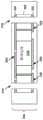
图1是根据本公开内容的一些示例的用于利用钻孔嵌在印刷电路板中的印刷电路板的等距视图;1 is an isometric view of a printed circuit board for embedding in a printed circuit board with drilled holes, according to some examples of the present disclosure;
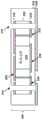
图2是根据本公开内容的一些示例的包括嵌入式印刷电路板和钻孔的印刷电路板的侧视图;2 is a side view of a printed circuit board including an embedded printed circuit board and drilled holes, according to some examples of the present disclosure;
图3A至图3F是说明根据本公开内容的一些示例的用于利用钻孔将芯片嵌在印刷电路板中的过程的侧视图;3A-3F are side views illustrating a process for embedding a chip in a printed circuit board using drilled holes, according to some examples of the present disclosure;
图4是示出根据本公开内容的一些示例的用于构造具有钻孔的器件的示例过程的流程图;4 is a flowchart illustrating an example process for constructing a device with a drilled hole, according to some examples of the present disclosure;
图5是示出根据本公开内容的一些示例的具有钻孔和金属芯的印刷电路板的侧视图;5 is a side view showing a printed circuit board with drilled holes and a metal core, according to some examples of the present disclosure;
图6是根据本公开内容的一些示例的具有被配置成用于钻孔的接触垫的印刷电路板的俯视图;6 is a top view of a printed circuit board with contact pads configured for drilling, according to some examples of the present disclosure;
图7是根据本公开内容的一些示例的具有嵌入式印刷电路的印刷电路板的俯视图。7 is a top view of a printed circuit board with embedded printed circuitry, according to some examples of the present disclosure.
具体实施方式Detailed ways
在一些系统中,使用金属层将嵌入式印刷电路板电连接至主印刷电路板。然而,在一些制造工艺中,将嵌入式印刷电路板的金属层连接至主印刷电路板可能不可行。例如,可以使用与主印刷电路板相比产生相对窄的间距(pitch)的金属层(例如,迹线中心之间的标称距离)的相对昂贵的工艺来制造嵌入式印刷电路板。因此,用于制造主印刷电路板的制造工艺可能不适于将主印刷电路板连接至嵌入式印刷电路板的金属层。此外,在该示例中,制造商可能需要将嵌入式印刷电路板与主印刷电路板对准,以确保金属层将嵌入式印刷电路板与主印刷电路板电连接。然而,用于制造主印刷电路板的制造工艺可能不适于对于嵌入式印刷电路板的窄间距金属层的对准。In some systems, a metal layer is used to electrically connect the embedded printed circuit board to the main printed circuit board. However, in some manufacturing processes it may not be feasible to connect the metal layers of the embedded PCB to the main PCB. For example, embedded printed circuit boards may be fabricated using relatively expensive processes that result in relatively narrow pitch metal layers (eg, nominal distance between trace centers) compared to the main printed circuit board. Therefore, the manufacturing process used to manufacture the main printed circuit board may not be suitable for connecting the main printed circuit board to the metal layers of the embedded printed circuit board. Also, in this example, the manufacturer may need to align the embedded PCB with the main PCB to ensure that the metal layer electrically connects the embedded PCB with the main PCB. However, the manufacturing process used to manufacture the main printed circuit board may not be suitable for the alignment of the narrow pitch metal layers of the embedded printed circuit board.
根据本文描述的实施方式,嵌入式印刷电路板可以被配置成用于钻孔以允许钻孔将嵌入式印刷电路板电耦合至主印刷电路板,而不是仅依靠金属层来连接嵌入式印刷电路板与主印刷电路板。According to embodiments described herein, the embedded printed circuit board may be configured for drilling to allow the drilled holes to electrically couple the embedded printed circuit board to the main printed circuit board, rather than relying solely on metal layers to connect the embedded printed circuit board with the main printed circuit board.
图1是根据本公开内容的一些示例的用于利用钻孔嵌在印刷电路板中的印刷电路板102的等距视图。如所示出的,印刷电路板102包括嵌入式集成电路110、接触垫120至124以及金属层130。FIG. 1 is an isometric view of a printed
印刷电路板102机械地支承电子部件并且电连接电子部件。例如,印刷电路板102可以包括在非导电衬底上形成的一个或更多个金属层。非导电衬底的示例可以包括(但不限于)玻璃纤维增强环氧树脂(例如玻璃纤维、FR4等)、PTFE(聚四氟乙烯)、PEN(聚萘二甲酸乙二醇酯)、PET(聚对苯二甲酸乙二醇酯)、BT层压材料(双马来酰亚胺三嗪)或另外的非导电衬底。可以使用粘合层将电子部件附接至印刷电路板102。这样的粘合层还可以在印刷电路板102与一个或更多个电子部件之间导电。如本文所使用的,粘合层可以包括导电膏、导电胶或任何其他合适的材料。虽然在图1的示例中没有示出,但是印刷电路板102可以包括一个或更多个表面安装的电子器件。这样的表面安装的电子器件可以安装至印刷电路板102并电连接至金属层130。The
印刷电路板102的电子部件之间的电连接可以通过焊接形成。焊接部件以形成电连接可以包括:在部件之间放置焊料,加热熔化焊料,以及使得焊料冷却以形成电连接。还可以用导电膏、导电带、导电环氧树脂和/或金属烧结将印刷电路板102的电子部件胶合或粘合在一起。电子部件之间的连接可以包括金属化的电镀激光通孔、焊料和/或高压/高频金属化接合例如扩散接合(bonding)。扩散接合可以包括电子部件之间的直接接合,其中,每个电子部件可以是半导体管芯。Electrical connections between electronic components of the printed
金属层130可以由导电材料形成。导电材料的示例可以包括但不限于铜或其他导电材料。金属层130可以包括以下项中的一个或更多个:嵌入式金属层、迹线、金属化层、夹片、带状物、管芯置盘、引线键合、铜柱、硅通孔、引线框架段和/或任何其他合适的金属部件。应该理解,金属层130的导电材料可以形成嵌入式集成电路110与接触垫120至124之间的连接。可以使用金属化的电镀激光通孔、焊料和/或高压/高频金属化接合(例如扩散接合)来形成这样的连接。The
印刷电路板102可以包括(未示出的)一个或更多个另外的金属层。此外,应当理解,印刷电路板102可以包括用于在印刷电路板102的不同金属层之间进行连接的一个或更多个通孔。然而,在一些示例中,印刷电路板102可以包括单层(例如,金属层130)。The printed
嵌入式集成电路110可以是包括一个或更多个半导体器件的半导体封装。半导体器件的示例可以包括但不限于二极管、晶体管或另外的半导体器件。晶体管的示例可以包括但不限于可控硅整流器(SCR)、场效应晶体管(FET)和双极结型晶体管(BJT)。FET的示例可以包括但不限于结型场效应晶体管(JFET)、金属氧化物半导体FET(MOSFET)、双栅极MOSFET、绝缘栅双极型晶体管(IGBT)、任何其他类型的FET或者前述的任意组合。MOSFET的示例可以包括但不限于PMOS、NMOS、DMOS或任何其他类型的MOSFET或者前述的任意组合。BJT的示例可以包括但不限于PNP、NPN、异质结或任何其他类型的BJT或者前述的任意组合。应该理解,晶体管可以包括高侧开关或低侧开关。另外,晶体管可以是电压控制的和/或电流控制的。电流控制的晶体管的示例可以包括但不限于氮化镓(GaN)MOSFET、BJT或其他电流控制的晶体管。在一些示例中,嵌入式集成电路110可以包括多于两个晶体管,例如在多相电力转换器或其他更复杂的电力电路中。例如,在多相电力转换器中,针对电力转换器的每个相位,嵌入式集成电路110可以具有一个高侧晶体管和一个低侧晶体管。Embedded
嵌入式集成电路110可以包括一个或更多个处理器,一个或更多个处理器包括一个或更多个微处理器、数字信号处理器(DSP)、专用集成电路(ASIC)、现场可编程门阵列(FPGA)或任何其他等效集成逻辑电路或离散逻辑电路以及这些部件的任意组合。术语“处理器”或“处理电路”通常可以单独地或与其他逻辑电路或任何其他等效电路组合来指代任何上述逻辑电路。在一些示例中,嵌入式集成电路110可以是一个或更多个模拟部件和一个或更多个数字部件的组合。例如,在一些情况下,集成电路110可以包括与用于控制晶体管的栅极的控制电路组合的一个或更多个晶体管。在一些情况下,集成电路110可以包括形成半桥的两个晶体管,集成电路110内可能具有控制器。在一些示例中,集成电路110可以包括在同一芯片上形成的晶体管和控制器,而在其他示例中,集成电路110可以包括在分离且分立的芯片中形成的晶体管和控制器。Embedded
嵌入式集成电路110可以完全或部分地被封装在印刷电路板102的模制化合物和/或任何其他合适的绝缘材料中。例如,嵌入式集成电路110可以完全或部分地被封装在印刷电路板102的芯层中。Embedded
接触垫120至124可以被配置成用于钻孔。例如,如所示出的,接触垫120至124可以与嵌入式集成电路110间隔开。此外,如所示出的,接触垫120至124被形成为具有比金属层130的迹线宽得多的宽度。此外,接触垫120至124沿着印刷电路板102的边缘布置。The
图2是根据本公开内容的一些示例的包括嵌入式印刷电路板202和钻孔208和209的印刷电路板240的侧视图。在图2的示例中,印刷电路板102可以是嵌入式印刷电路板202和嵌入式印刷电路板203的示例。例如,印刷电路板202可以包括通过金属层电连接至一个或更多个接触垫的嵌入式集成电路。如所示出的,印刷电路板240可以包括:金属层242、246、252和256;芯层244、254;以及预浸渍(在本文中还被称为“预浸料”)层248。金属层242、246、252和256可以基本上类似于图1的金属层130。例如,金属层242、246、252和256可以由导电材料形成。虽然图2的示例示出了两块嵌入式印刷电路板,但是应该理解,在其他示例中可以使用更少的嵌入式印刷电路板(例如1块)或附加的嵌入式印刷电路板(例如,3块或更多块)。2 is a side view of printed
芯层244和254可以由非导电衬底形成。例如,芯层244和254可以各自包括一个或更多个介电层。如所示出的,芯层244将嵌入式印刷电路板202与金属层242和246间隔开。类似地,芯层254将嵌入式印刷电路板203与金属层252和256间隔开。芯层244和254可以包括具有非导电衬底材料的大致平坦的预制板。Core layers 244 and 254 may be formed from a non-conductive substrate. For example, core layers 244 and 254 may each include one or more dielectric layers. As shown,
在图2的示例性过程中,在形成芯层244之后,该过程在芯层244之下形成金属层246并且在芯层244之上形成金属层242。例如,如所示出的,该过程可以直接在芯层244的上表面上形成金属层242。应该理解,直接在第二层上形成第一层可以包括施加用于将第一层和第二层接合在一起的一种或更多种材料。此外,如所示出的,该过程可以直接在芯层244的下表面上形成金属层246。In the exemplary process of FIG. 2 , after forming
类似地,在形成芯层254之后,该过程在芯层254之下形成金属层256并且在芯层254之上形成金属层252。例如,如所示出的,该过程可以直接在金属层252的上表面上形成金属层252。此外,如所示出的,该过程可以直接在芯层254的下表面上形成金属层256。Similarly, after forming
预浸渍层248可以机械地耦合金属层246和252,同时电隔离金属层246和252。例如,该过程可以直接在金属层246的下表面上形成预浸渍层248。类似地,该过程可以直接在金属层252的上表面上形成预浸渍层248。
可以通过在印刷电路板240中钻孔以形成空腔并在空腔中形成导电材料来形成钻孔208和209。如所示出的,钻孔208延伸穿过嵌入式印刷电路板202。以这种方式,钻孔208可以将嵌入式印刷电路板202电耦合至金属层242、246、252和256。类似地,钻孔209延伸穿过嵌入式印刷电路板203。以这种方式,钻孔209可以将嵌入式印刷电路板203电耦合至金属层242、246、252和256。
可以对印刷电路板240执行进一步的处理。例如,一个或更多个表面安装的电子器件可以安装至印刷电路板240上。此外,可以在印刷电路板240的顶表面上形成介电层。类似地,可以在印刷电路板240的底表面上形成介电层。应该理解,嵌入式印刷电路板202和/或203可以包括表面安装的电子器件。例如,嵌入式印刷电路板202可以包括一个或更多个表面安装的电子器件。另外地或可替选地,嵌入式印刷电路板203可以包括一个或更多个表面安装的电子器件。Further processing may be performed on printed
根据本公开内容的技术,印刷电路板240可以是包括第一印刷电路板、第二印刷电路板以及一个或更多个钻孔的半导体器件的示例。第一印刷电路板包括嵌入式集成电路、一个或更多个金属层以及一个或更多个接触垫。嵌入式集成电路通过一个或更多个金属层电连接至一个或更多个接触垫。第一印刷电路板具有顶表面和与顶表面相对的底表面。第二印刷电路板包括布置在底表面之下的一个或更多个第一金属层。一个或更多个第一介电层将用于第二印刷电路板的一个或更多个第一金属层与第一印刷电路板的一个或更多个金属层间隔开。第二印刷电路板还包括布置在顶表面之上的一个或更多个第二金属层。一个或更多个第二介电层将用于第二印刷电路板的一个或更多个第二金属层与第一印刷电路板的一个或更多个金属层间隔开。一个或更多个钻孔中的每个钻孔穿过一个或更多个接触垫中的相应接触垫从底表面延伸至顶表面,并且每个钻孔包括导电材料,导电材料将第一印刷电路板的一个或更多个接触垫中的相应接触垫电耦合至第二印刷电路板。According to the techniques of the present disclosure, the printed
图3A至图3F是示出根据本公开内容的一些示例的用于利用钻孔将芯片嵌在印刷电路板中的过程的侧视图。图3A至图3F所示的过程可以由印刷电路板制造商执行。3A-3F are side views illustrating a process for embedding a chip in a printed circuit board using drilled holes according to some examples of the present disclosure. The process shown in FIGS. 3A-3F may be performed by a printed circuit board manufacturer.
在图3A的示例中,该过程提供印刷电路板302。如图3A所示,印刷电路板302包括嵌入式集成电路310、金属层330和332以及接触垫320和322。虽然图3A至图3F的示例性过程示出了两个接触垫,但是在其他示例中可以包括更少的接触垫(例如,一个接触垫)或附加的接触垫(例如,两个或更多个接触垫)。如所示出的,接触垫320和322可以布置在底表面350上。另外或可替选地,接触垫可以布置在顶表面352上。例如,如所示出的,印刷电路板302可以包括布置在顶表面352上的接触垫321和323。应该理解,对于接触垫320和322以及对于接触垫321和323,图3A至图3F所示的过程可以基本上类似。在一些示例中,可以省略接触垫321和323,并且可以将接触垫320和322包括在印刷电路板302中。类似地,在一些示例中,可以省略接触垫320和322,并且可以将接触垫321和323包括在印刷电路板302中。In the example of FIG. 3A , the process provides printed
应该理解,可以使用与图3A至图3F所示的制造工艺不同的制造工艺来制造印刷电路板302。例如,可以使用相对窄的间距的制造工艺来制造印刷电路板302,并且可以使用相对宽的间距的制造工艺来执行过程400。宽间距制造工艺的示例可以包括:产生大于200微米(μm)的通孔尺寸的制造工艺、产生大于300微米(μm)的通孔至通孔间距的制造工艺或另外的宽间距制造工艺。窄间距制造工艺的示例可以包括:使用钻孔产生小于200微米(μm)的通孔尺寸的制造工艺、使用激光钻孔产生小于100微米(μm)的通孔尺寸的制造工艺、产生200微米(μm)或更小的窄间距(通孔至通孔)的制造工艺或者另外的窄间距制造工艺。It should be understood that the printed
在图3B的示例中,该过程将印刷电路板302嵌在芯层344中。例如,图3B所示的过程可以在印刷电路板302周围形成非导电衬底。例如,该过程可以将用于非导电衬底的材料直接施加至印刷电路板302的底表面、顶表面和侧表面上。在一些示例中,该过程可以形成芯层344的具有开口的一部分,其中开口被定尺寸和成形以容纳印刷电路板302,并且该过程将印刷电路板302布置在开口中。例如,该过程可以将该开口切割成芯层344的基本上共同参与的(coplayer)部分,并将印刷电路板302布置在该开口中。在一些情况下,该过程可以直接形成芯层344的具有开口的部分。在任何情况下,该过程都可以在印刷电路板302之下形成介电层334。应该理解,印刷电路板302可以省略表面可安装触点,并且作为替代,依靠接触垫320和322来电连接印刷电路板302。在该示例中,该过程可以在印刷电路板302上形成芯层344的一部分,使得印刷电路板302由芯层344封装。例如,该过程可以在印刷电路板302上形成介电层336。In the example of FIG. 3B , the process embeds printed
在图3C的示例中,该过程在接触垫320中钻出空腔314并且在接触垫322中钻出空腔316。如所示出的,空腔314可以穿过印刷电路板302的顶表面352延伸至印刷电路板302的底表面350。此外,空腔314可以延伸穿过芯层344。类似地,空腔316可以穿过印刷电路板302的顶表面352延伸至印刷电路板302的底表面350。此外,空腔316可以延伸穿过芯层344。In the example of FIG. 3C , the process drills
在图3D的示例中,该过程在印刷电路板302的底表面350之下形成用于第二印刷电路板的第一金属层346。如所示出的,介电层334将金属层332与金属层346间隔开。虽然图3D的示例在底表面350之下包括一个金属层(例如,金属层332),但是应该理解,在一些示例中,可以在底表面350之下形成多于一个金属层。In the example of FIG. 3D , the process forms the
在图3E的示例中,该过程形成钻孔364和366。例如,该过程通过在图3D的空腔314中提供导电材料来形成钻孔364。类似地,该过程通过在图3C的空腔316中提供导电材料来形成钻孔366。接触垫320和322可以由与用于形成钻孔364和366的导电材料相同的导电材料形成。通过使用相同的导电材料形成钻孔364与接触垫320,接触垫320与钻孔364之间的连接可能不需要焊接。类似地,通过使用相同的导电材料来形成钻孔366与接触垫322,接触垫322与钻孔366之间的连接可能不需要焊接。虽然图3E的示例示出了金属层346可以电耦合至钻孔364和钻孔366,但是在一些示例中,金属层346可以与钻孔364和/或钻孔366电隔离。In the example of FIG. 3E , the process forms
在图3F的示例中,该过程在印刷电路板302的顶表面352之上形成金属层342以形成印刷电路板340。如所示出的,介电层336将金属层330与金属层342间隔开。虽然图3F的示例在顶表面352之上包括一个金属层(例如,金属层342),但是应该理解,在一些示例中,可以在顶表面352之上形成多于一个金属层。另外,虽然图3F的示例示出了金属层342可以电耦合至钻孔364和钻孔366,但是在一些示例中,金属层342可以与钻孔364和/或钻孔366电隔离。In the example of FIG. 3F , the process forms
应该理解,可以对印刷电路板340执行进一步的处理。例如,一个或更多个表面安装的电子器件可以安装至印刷电路板340上。这样的表面安装的电子器件可以安装至印刷电路板340并且电连接至金属层330、332、342和346中的一个或更多个。另外或可替选地,这样的表面安装的电子器件可以安装至印刷电路板340并且电连接至钻孔364和366中的一个或更多个。此外,可以在印刷电路板340的顶表面上形成介电层。类似地,可以在印刷电路板340的底表面上形成介电层。It should be understood that further processing may be performed on printed
虽然图3A至图3F示出了金属层330和332电耦合至钻孔364和366,但是在一些示例中,仅一个或更多个顶层可以电耦合至钻孔364和366。例如,可以省略接触垫320和322。在一些示例中,仅一个或更多个底层可以电耦合至钻孔364和366。例如,可以省略接触垫321和323。Although FIGS. 3A-3F illustrate
根据本公开内容的技术,印刷电路板340可以是包括第一印刷电路板、第二印刷电路板以及一个或更多个钻孔的半导体器件的示例。第一印刷电路板包括嵌入式集成电路、一个或更多个金属层以及一个或更多个接触垫。嵌入式集成电路通过一个或更多个金属层电连接至一个或更多个接触垫。第一印刷电路板具有顶表面和与顶表面相对的底表面。第二印刷电路板包括布置在所述底表面之下的一个或更多个第一金属层。一个或更多个第一介电层将用于第二印刷电路板的一个或更多个第一金属层与第一印刷电路板的一个或更多个金属层间隔开。第二印刷电路板还包括布置在所述顶表面之上的一个或更多个第二金属层。一个或更多个第二介电层将用于第二印刷电路板的一个或更多个第二金属层与第一印刷电路板的一个或更多个金属层间隔开。一个或更多个钻孔中的每个钻孔穿过一个或更多个接触垫中的相应接触垫从底表面延伸至顶表面,并且每个钻孔包括导电材料,导电材料将第一印刷电路板的一个或更多个接触垫中的相应接触垫电耦合至第二印刷电路板。According to the techniques of the present disclosure, the printed
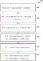
图4是示出根据本公开内容的一些示例的用于构造具有钻孔的器件的示例过程的流程图。仅出于示例性目的,参考图3A至图3F描述图4的过程。4 is a flowchart illustrating an example process for fabricating a device with a drilled hole, according to some examples of the present disclosure. For exemplary purposes only, the process of FIG. 4 is described with reference to FIGS. 3A-3F .
过程400提供包括嵌入式集成电路的第一印刷电路板(402)。例如,可以使用窄间距制造工艺来制造图3A的印刷电路板302。过程400将第一印刷电路板形成在用于第二印刷电路板的芯层中(404)。例如,宽间距制造工艺将电介质结合到图3A的印刷电路板302的底表面和顶表面上,使得印刷电路板302被电介质密封。
过程400在第一印刷电路板中钻出一个或更多个空腔(406)。例如,宽间距制造工艺钻入接触垫320以形成图3C的空腔314。类似地,宽间距制造工艺可以钻入接触垫322以形成图3C的空腔316。Process 400 drills one or more cavities in the first printed circuit board (406). For example, a wide-pitch manufacturing process drills into
过程400在第一印刷电路板的底表面上形成用于第二印刷电路板的一个或更多个层(408)。例如,宽间距制造工艺在印刷电路板302的底表面350之下形成图3D的金属层346。过程400在一个或更多个空腔中形成导电材料(410)。例如,宽间距制造工艺通过在图3D的空腔314中提供导电材料来形成图3E的钻孔364。类似地,宽间距制造工艺通过在图3D的空腔316中提供导电材料来形成图3E的钻孔366。过程400在第一印刷电路板的顶表面上形成用于第二印刷电路板的一个或更多个层(412)。例如,宽间距制造工艺在印刷电路板302的顶表面352之上形成图3F的金属层342,以形成印刷电路板340。Process 400 forms one or more layers for a second printed circuit board on a bottom surface of the first printed circuit board (408). For example, a wide-pitch manufacturing process forms
应该理解,虽然过程400在形成用于第二印刷电路板的第一金属层之前在第一印刷电路板中钻出一个或更多个空腔,但是在一些示例中,可以在形成用于第二印刷电路板的第一金属层之后执行在第一印刷电路板中钻出一个或更多个空腔。例如,如图2所示,一些工艺可以在形成用于第二印刷电路板的第一金属层之后(并且在形成用于第二印刷电路板的第二金属层之后)在第一印刷电路板中钻出一个或更多个空腔。例如,在图2的示例中,过程可以通过钻入印刷电路板240来钻出用于钻孔208和209的空腔。以这种方式,钻孔208可以延伸穿过第二印刷电路板的至少一部分。例如,图2的钻孔208和209可以延伸穿过印刷电路板240的金属层242、246、252和256。It should be appreciated that while
根据本公开内容的技术,过程400可以是包括在第一印刷电路板的一个或更多个接触垫的每个接触垫中钻出空腔以形成一个或更多个空腔的方法的示例。第一印刷电路板包括嵌入式集成电路和一个或更多个金属层。嵌入式集成电路通过一个或更多个金属层电连接至一个或更多个接触垫。该方法还包括在第一印刷电路板的底表面之下形成用于第二印刷电路板的一个或更多个第一金属层。一个或更多个第一介电层将第一印刷电路板的一个或更多个金属层与用于第二印刷电路板的一个或更多个第一金属层间隔开。该方法还包括在一个或更多个空腔中形成导电材料。导电材料将第一印刷电路板的一个或更多个接触垫电耦合至第二印刷电路板。该方法还包括在第一印刷电路板的顶表面之上形成用于第二印刷电路板的一个或更多个第二金属层。顶表面与底表面相对。一个或更多个第二介电层将第一印刷电路板的一个或更多个金属层与用于第二印刷电路板的一个或更多个第二金属层间隔开。
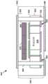
图5是示出根据本公开内容的一些示例的具有钻孔564和566以及金属芯570的印刷电路板540的侧视图。如图所示,印刷电路板540可以包括芯层544、金属层542和546、钻孔564和566以及印刷电路板502。芯层544可以基本上类似于图3A至图3F的芯层344。例如,芯层544可以由非导电衬底形成。金属层542和546可以基本上类似于图3A至图3F的金属层342和346。例如,金属层542和546可以由导电材料形成。钻孔564和566可以基本上分别类似于图3A至3F的钻孔364和366。例如,钻孔564和566可以通过钻出空腔并将导电材料设置在空腔中来形成。尽管图5的示例示出了一个嵌入式印刷电路板,但应该理解,在其他示例中可以使用另外的(例如,或更多的)嵌入式印刷电路板。5 is a side view illustrating a printed
印刷电路板502可以包括通过金属层530和532而电连接至接触垫520和522的嵌入式集成电路510。嵌入式集成电路510、接触垫520和522以及金属层530和532可以基本上分别类似于图3A至图3F的嵌入式集成电路310、接触垫320和322以及金属层330和332。然而,印刷电路板502还可以包括金属芯570。另外地或替选地,印刷电路板502可以包括布置在印刷电路板502的顶表面上的基本上类似于图3A的接触垫321和323的接触垫。Printed
金属芯570可以使用粘附层来附接至印刷电路板502。这样的粘附层也可以在印刷电路板502与一个或更多个电子部件之间导电。此外,如所示,金属芯570可以被完全封装在印刷电路板540的模塑料和/或任何其他合适的绝缘材料中。例如,金属芯570可以被完全或部分地封装在印刷电路板540的芯层544中。
金属芯570可以是电感器。因此,金属芯570可以阻止交流(AC)电流的流动,同时允许直流(DC)电流流过金属芯570。在一些示例中,金属芯570可以电耦合至集成电路510。在一些示例中,金属芯570可以与印刷电路板540电隔离。例如,介电层536可以将印刷电路板540与金属芯570电隔离。
根据本公开内容的技术,印刷电路板540可以是包括第一印刷电路板、第二印刷电路板以及一个或更多个钻孔的半导体器件的示例。第一印刷电路板包括嵌入式集成电路、一个或更多个金属层以及一个或更多个接触垫。嵌入式集成电路通过一个或更多个金属层来电连接至一个或更多个接触垫。第一印刷电路板具有顶表面和与顶表面相对的底表面。第二印刷电路板包括布置在底表面之下的一个或更多个第一金属层。一个或更多个第一介电层将用于第二印刷电路板的一个或更多个第一金属层与第一印刷电路板的一个或更多个金属层间隔开。第二印刷电路板还包括布置在顶表面之上的一个或更多个第二金属层。一个或更多个第二介电层将用于第二印刷电路板的一个或更多个第二金属层与第一印刷电路板的一个或更多个金属层间隔开。一个或更多个钻孔中的每个钻孔穿过一个或更多个接触垫中的相应接触垫从底表面延伸至顶表面,并且每个钻孔包括导电材料,导电材料将第一印刷电路板的一个或更多个接触垫中的相应接触垫电耦合至第二印刷电路板。According to the techniques of the present disclosure, the printed
图6是根据本公开内容的一些示例的具有被配置成用于钻孔的接触垫620至622的印刷电路板602的俯视图。在图6的示例中,印刷电路板602可以是印刷电路板302的示例。印刷电路板602可以包括管芯672、674和676。例如,管芯672包括嵌入式集成电路。在一些示例中,管芯674可以包括一个或更多个晶体管。在一些示例中,管芯676可以包括一个或更多个晶体管。在图6的示例中,接触垫620通过一个或更多个金属层来电连接至管芯672。类似地,在一些示例中,接触垫621通过一个或更多个金属层来电连接至管芯674。此外,在一些示例中,接触垫622通过一个或更多个金属层来电连接至管芯676。6 is a top view of a printed
印刷电路板602可以被配置用于任何合适的应用。例如,管芯672可以包括用于电压调节的嵌入式集成电路。在该示例中,管芯674和676可以包括用于对用于电压调节的开关功率转换器进行切换的晶体管。在一些示例中,管芯672可以包括用于控制半桥或功率级转换器的嵌入式集成电路。在该示例中,管芯674和676可以包括用于半桥或功率级转换器的晶体管。Printed
图7是根据本公开内容的一些示例的具有嵌入式印刷电路板702的印刷电路板740的俯视图。在图7的示例中,印刷电路板740可以是印刷电路板340的示例。印刷电路板740可以包括印刷电路板702和接触垫780-782。7 is a top view of a printed
印刷电路板702可以基本上类似于图6的印刷电路板602。在图7的示例中,印刷电路板702可以包括:包括嵌入式集成电路的管芯772;包括晶体管的管芯774以及包括晶体管的管芯776。在该示例中,接触垫720可以被钻孔以形成空腔,该空腔可以被填充有导电材料以形成钻孔。类似地,接触垫721可以被钻孔以形成空腔,该空腔可以被填充有导电材料以形成钻孔。此外,接触垫722可以被钻孔以形成空腔,该空腔可以被填充有导电材料以形成钻孔。Printed
在图7的示例中,接触垫780通过一个或更多个金属层来电连接至接触垫720。类似地,在一些示例中,接触垫781通过一个或更多个金属层来电连接至接触垫721。此外,在一些示例中,接触垫782通过一个或更多个金属层来电连接至接触垫722。In the example of FIG. 7 ,
应当理解,钻孔可以形成到接触垫780-782中。例如,接触垫780可以被钻孔以形成空腔,该空腔可以被填充有导电材料以形成钻孔。类似地,接触垫781被可以钻孔以形成空腔,该空腔可以被填充有导电材料以形成钻孔。此外,接触垫782可以被钻孔以形成空腔,该空腔可以被填充有导电材料以形成钻孔。以该方式,印刷电路板740可以被嵌在(未示出的)另一个印刷电路板中。It should be understood that drilled holes may be formed into the contact pads 780-782. For example,
根据本公开内容的技术,印刷电路板740可以是包括第一印刷电路板、第二印刷电路板以及一个或更多个钻孔的半导体器件的示例。第一印刷电路板包括:嵌入式集成电路、包括晶体管的第二管芯、一个或更多个金属层以及一个或更多个接触垫。第一管芯和第二管芯通过一个或更多个金属层来电连接至一个或更多个接触垫。第一印刷电路板具有顶表面和与顶表面相对的底表面。第二印刷电路板包括布置在底表面之下的一个或更多个第一金属层。一个或更多个第一介电层将用于第二印刷电路板的一个或更多个第一金属层与第一印刷电路板的一个或更多个金属层间隔开。第二印刷电路板还包括布置在顶表面之上的一个或更多个第二金属层。一个或更多个第二介电层将用于第二印刷电路板的一个或更多个第二金属层与第一印刷电路板的一个或更多个金属层间隔开。一个或更多个钻孔中的每个钻孔穿过一个或更多个接触垫中的相应接触垫从底表面延伸至顶表面,并且每个钻孔包括导电材料,导电材料将第一印刷电路板的一个或更多个接触垫中的相应接触垫电耦合至第二印刷电路板。According to the techniques of the present disclosure, the printed
下面的示例可以说明本公开内容的一个或更多个方面。The following examples may illustrate one or more aspects of the present disclosure.
示例1.一种方法,包括:在第一印刷电路板的一个或更多个接触垫中的每个接触垫中钻出空腔以形成一个或更多个空腔,其中,第一印刷电路板包括嵌入式集成电路和一个或更多个金属层,并且其中,嵌入式集成电路通过一个或更多个金属层来电连接至一个或更多个接触垫;在第一印刷电路板的底表面之下形成用于第二印刷电路板的一个或更多个第一金属层,其中,一个或更多个第一介电层将第一印刷电路板的一个或更多个金属层与用于第二印刷电路板的一个或更多个第一金属层间隔开;在一个或更多个空腔中形成导电材料,所述导电材料将第一印刷电路板的一个或更多个接触垫电耦合至第二印刷电路板;以及在第一印刷电路板的顶表面之上形成用于第二印刷电路板的一个或更多个第二金属层,其中,顶表面与底表面相对,并且其中,一个或更多个第二介电层将第一印刷电路板的一个或更多个金属层与用于第二印刷电路板的一个或更多个第二金属层间隔开。Example 1. A method comprising: drilling a cavity in each of one or more contact pads of a first printed circuit board to form the one or more cavities, wherein the first printed circuit board The board includes an embedded integrated circuit and one or more metal layers, and wherein the embedded integrated circuit is electrically connected to the one or more contact pads through the one or more metal layers; on the bottom surface of the first printed circuit board One or more first metal layers for the second printed circuit board are formed below, wherein the one or more first dielectric layers connect the one or more metal layers of the first printed circuit board with the The one or more first metal layers of the second printed circuit board are spaced apart; forming a conductive material in the one or more cavities that connects the one or more contact pads of the first printed circuit board electrically coupled to a second printed circuit board; and forming one or more second metal layers for the second printed circuit board over a top surface of the first printed circuit board, wherein the top surface is opposite the bottom surface, and Therein, the one or more second dielectric layers separate the one or more metal layers for the first printed circuit board from the one or more second metal layers for the second printed circuit board.
示例2.根据示例1的方法,其中,导电材料将第一印刷电路板的一个或更多个接触垫电耦合至一个或更多个第一金属层。Example 2. The method of example 1, wherein the conductive material electrically couples the one or more contact pads of the first printed circuit board to the one or more first metal layers.
示例3.根据示例1至2的任何组合的方法,其中,导电材料将第一印刷电路板的一个或更多个接触垫电耦合至一个或更多个第二金属层。Example 3. The method of any combination of examples 1 to 2, wherein the conductive material electrically couples the one or more contact pads of the first printed circuit board to the one or more second metal layers.
示例4.根据示例1至3的任何组合的方法,其中,第一印刷电路板的一个或更多个金属层具有与用于第二印刷电路板的一个或更多个第一金属层相比更窄的间距,并且其中,第一印刷电路板的一个或更多个金属层具有与用于第二印刷电路板的一个或更多个第二金属层相比更窄的间距。Example 4. The method of any combination of examples 1 to 3, wherein the one or more metal layers of the first printed circuit board have an a narrower pitch, and wherein the one or more metal layers of the first printed circuit board have a narrower pitch than the one or more second metal layers used for the second printed circuit board.
示例5.根据示例1至4的任何组合的方法,其中,第一印刷电路板的一个或更多个金属层是第一印刷电路板的多个金属层,并且其中,在一个或更多个接触垫中的每个接触垫中钻出空腔包括钻穿多个金属层。Example 5. The method of any combination of examples 1 to 4, wherein the one or more metal layers of the first printed circuit board is a plurality of metal layers of the first printed circuit board, and wherein the one or more Drilling a cavity in each of the contact pads includes drilling through a plurality of metal layers.
示例6.根据示例1至5的任何组合的方法,其中,第一印刷电路板包括金属芯,并且其中,形成一个或更多个第二金属层包括将金属芯嵌在第二印刷电路板中。Example 6. The method of any combination of examples 1 to 5, wherein the first printed circuit board includes a metal core, and wherein forming the one or more second metal layers comprises embedding the metal core in the second printed circuit board .
示例7.根据示例1至6的任何组合的方法,其中,金属芯电耦合至嵌入式集成电路,并且其中,金属芯与第二印刷电路板电隔离。Example 7. The method of any combination of examples 1 to 6, wherein the metal core is electrically coupled to the embedded integrated circuit, and wherein the metal core is electrically isolated from the second printed circuit board.
示例8.根据示例1至7的任何组合的方法,其中,金属芯是电感器。Example 8. The method of any combination of examples 1 to 7, wherein the metal core is an inductor.
示例9.根据示例1至8的任何组合的方法,其中,第一印刷电路板包括嵌在第一印刷电路板中的第三印刷电路板,第三印刷电路板包括嵌入式集成电路。Example 9. The method of any combination of examples 1 to 8, wherein the first printed circuit board comprises a third printed circuit board embedded in the first printed circuit board, the third printed circuit board comprising embedded integrated circuits.
示例10.一种半导体器件,包括:第一印刷电路板,其包括嵌入式集成电路、一个或更多个金属层以及一个或更多个接触垫,嵌入式集成电路通过一个或更多个金属层来电连接至一个或更多个接触垫,其中,第一印刷电路板具有顶表面和与顶表面相对的底表面;第二印刷电路板,其包括:布置在底表面之下的一个或更多个第一金属层,其中,一个或更多个第一介电层将用于第二印刷电路板的一个或更多个第一金属层与第一印刷电路板的一个或更多个金属层间隔开,以及布置在顶表面之上的一个或更多个第二金属层,其中,一个或更多个第二介电层将用于第二印刷电路板的一个或更多个第二金属层与第一印刷电路板的一个或更多个金属层间隔开;以及一个或更多个钻孔,一个或更多个钻孔中的每个钻孔穿过一个或更多个接触垫中的相应接触垫从底表面延伸至顶表面,并且每个钻孔包括导电材料,导电材料将第一印刷电路板的一个或更多个接触垫中的相应接触垫电耦合至第二印刷电路板。Example 10. A semiconductor device comprising: a first printed circuit board comprising an embedded integrated circuit, one or more metal layers, and one or more contact pads, the embedded integrated circuit passing through the one or more metal layers The layer is electrically connected to one or more contact pads, wherein the first printed circuit board has a top surface and a bottom surface opposite to the top surface; the second printed circuit board includes: one or more contact pads arranged below the bottom surface A plurality of first metal layers, wherein one or more first dielectric layers will be used for the one or more first metal layers of the second printed circuit board and the one or more metal layers of the first printed circuit board The layers are spaced apart, and one or more second metal layers are arranged on the top surface, wherein one or more second dielectric layers will be used for one or more second metal layers of the second printed circuit board. Two metal layers are spaced apart from the one or more metal layers of the first printed circuit board; and one or more bores, each of the one or more bores passing through one or more A respective one of the contact pads extends from the bottom surface to the top surface, and each bore includes a conductive material that electrically couples a respective one of the one or more contact pads of the first printed circuit board to the second printed circuit board. A printed circuit board.
示例11.根据示例10的器件,其中,导电材料将一个或更多个接触垫电耦合至一个或更多个第一金属层。Example 11. The device of example 10, wherein the conductive material electrically couples the one or more contact pads to the one or more first metal layers.
示例12.根据示例10至11的任何组合的器件,其中,导电材料将一个或更多个接触垫电耦合至一个或更多个第二金属层。Example 12. The device of any combination of examples 10 to 11, wherein the conductive material electrically couples the one or more contact pads to the one or more second metal layers.
示例13.根据示例10至12的任何组合的器件,其中,第一印刷电路板的一个或更多个金属层具有与用于第二印刷电路板的一个或更多个第一金属层相比更窄的间距,并且其中,第一印刷电路板的一个或更多个金属层具有与用于第二印刷电路板的一个或更多个第二金属层相比更窄的间距。Example 13. The device of any combination of examples 10 to 12, wherein the one or more metal layers of the first printed circuit board have an a narrower pitch, and wherein the one or more metal layers of the first printed circuit board have a narrower pitch than the one or more second metal layers used for the second printed circuit board.
示例14.根据示例10至13的任何组合的器件,其中,第一印刷电路板的一个或更多个金属层是第一印刷电路板的多个金属层,并且其中,导电材料延伸穿过多个金属层。Example 14. The device of any combination of examples 10 to 13, wherein the one or more metal layers of the first printed circuit board are multiple metal layers of the first printed circuit board, and wherein the conductive material extends through multiple a metal layer.
示例15.根据示例10至14的任何组合的器件,其中,第一印刷电路板包括金属芯,并且其中,一个或更多个第二金属层将金属芯嵌在第二印刷电路板中。Example 15. The device of any combination of examples 10 to 14, wherein the first printed circuit board includes a metal core, and wherein the one or more second metal layers embed the metal core in the second printed circuit board.
示例16.根据示例10至15的任何组合的器件,其中,金属芯电耦合至嵌入式集成电路,并且其中,金属芯与第二印刷电路板电隔离。Example 16. The device of any combination of examples 10 to 15, wherein the metal core is electrically coupled to the embedded integrated circuit, and wherein the metal core is electrically isolated from the second printed circuit board.
示例17.根据示例10至16的任何组合的器件,其中,金属芯是电感器。Example 17. The device of any combination of examples 10 to 16, wherein the metal core is an inductor.
示例18.根据示例10至17的任何组合的器件,其中,第一印刷电路板包括嵌在第一印刷电路板中的第三印刷电路板,第三印刷电路板包括嵌入式集成电路。Example 18. The device of any combination of examples 10 to 17, wherein the first printed circuit board comprises a third printed circuit board embedded in the first printed circuit board, the third printed circuit board comprising an embedded integrated circuit.
示例19.一种器件,包括:第一印刷电路板,其包括:包括嵌入式集成电路的第一管芯、包括晶体管的第二管芯、一个或更多个金属层以及一个或更多个接触垫,其中,第一管芯和第二管芯通过一个或更多个金属层电连接至一个或更多个接触垫,并且其中,第一印刷电路板具有顶表面和与顶表面相对的底表面;第二印刷电路板,其包括:布置在底表面之下的一个或更多个第一金属层,其中,一个或更多个第一介电层将用于第二印刷电路板的一个或更多个第一金属层与第一印刷电路板的一个或更多个金属层间隔开,以及布置在顶表面之上的一个或更多个第二金属层,其中,一个或更多个第二介电层将用于第二印刷电路板的一个或更多个第二金属层与第一印刷电路板的一个或更多个金属层间隔开;以及一个或更多个钻孔,一个或更多个钻孔中的每个钻孔穿过一个或更多个接触垫中的相应接触垫从底表面延伸至顶表面,并且每个钻孔包括导电材料,导电材料将第一印刷电路板的一个或更多个接触垫中的相应接触垫电耦合至第二印刷电路板。Example 19. A device comprising: a first printed circuit board comprising: a first die comprising embedded integrated circuits, a second die comprising transistors, one or more metal layers, and one or more Contact pads, wherein the first die and the second die are electrically connected to the one or more contact pads through one or more metal layers, and wherein the first printed circuit board has a top surface and a bottom surface; a second printed circuit board comprising: one or more first metal layers arranged below the bottom surface, wherein one or more first dielectric layers will be used for the second printed circuit board One or more first metal layers are spaced apart from the one or more metal layers of the first printed circuit board, and one or more second metal layers are disposed on the top surface, wherein the one or more a plurality of second dielectric layers space the one or more second metal layers for the second printed circuit board from the one or more metal layers of the first printed circuit board; Each of the one or more boreholes extends from the bottom surface to the top surface through a corresponding one of the one or more contact pads, and each borehole includes a conductive material that connects the first Respective ones of the one or more contact pads of one printed circuit board are electrically coupled to a second printed circuit board.
示例20.根据示例19的器件,其中,第一印刷电路板包括嵌在第一印刷电路板中的第三印刷电路板,第三印刷电路板包括第一管芯和第二管芯。Example 20. The device of example 19, wherein the first printed circuit board includes a third printed circuit board embedded in the first printed circuit board, the third printed circuit board including the first die and the second die.
已经在本公开内容中描述了各个方面。这些方面和其他方面在所附权利要求的范围内。Various aspects have been described in this disclosure. These and other aspects are within the scope of the appended claims.
Claims (20)
Applications Claiming Priority (2)
| Application Number | Priority Date | Filing Date | Title |
|---|---|---|---|
| US15/633,154US10206286B2 (en) | 2017-06-26 | 2017-06-26 | Embedding into printed circuit board with drilling |
| US15/633,154 | 2017-06-26 |
Publications (2)
| Publication Number | Publication Date |
|---|---|
| CN109121291A CN109121291A (en) | 2019-01-01 |
| CN109121291Btrue CN109121291B (en) | 2023-07-04 |
Family
ID=62712775
Family Applications (1)
| Application Number | Title | Priority Date | Filing Date |
|---|---|---|---|
| CN201810613513.8AActiveCN109121291B (en) | 2017-06-26 | 2018-06-14 | Semiconductor device and method for constructing semiconductor device |
Country Status (3)
| Country | Link |
|---|---|
| US (2) | US10206286B2 (en) |
| EP (1) | EP3422824A1 (en) |
| CN (1) | CN109121291B (en) |
Families Citing this family (3)
| Publication number | Priority date | Publication date | Assignee | Title |
|---|---|---|---|---|
| JP2021040021A (en)* | 2019-09-03 | 2021-03-11 | 富士通インターコネクトテクノロジーズ株式会社 | Substrates, substrate manufacturing methods, and electronic devices |
| CN112738994B (en)* | 2020-11-24 | 2022-12-09 | 鹤山市世拓电子科技有限公司 | Printed circuit board with embedded power device |
| JP7581915B2 (en)* | 2021-01-26 | 2024-11-13 | セイコーエプソン株式会社 | Vibration device and method for manufacturing the same |
Citations (6)
| Publication number | Priority date | Publication date | Assignee | Title |
|---|---|---|---|---|
| JPH03159193A (en)* | 1989-11-16 | 1991-07-09 | Sanyo Electric Co Ltd | Hybrid integrated circuit device |
| US5111278A (en)* | 1991-03-27 | 1992-05-05 | Eichelberger Charles W | Three-dimensional multichip module systems |
| JP2006178489A (en)* | 2006-01-16 | 2006-07-06 | Ibiden Co Ltd | Device for optical communication |
| KR20090096809A (en)* | 2008-03-10 | 2009-09-15 | 대덕전자 주식회사 | Method for manufacturing printed circuit board embedded with semiconductor parts |
| KR20110067449A (en)* | 2009-12-14 | 2011-06-22 | 삼성전기주식회사 | Printed circuit board and manufacturing method thereof |
| USRE45637E1 (en)* | 2005-08-29 | 2015-07-28 | Stablcor Technology, Inc. | Processes for manufacturing printed wiring boards |
Family Cites Families (26)
| Publication number | Priority date | Publication date | Assignee | Title |
|---|---|---|---|---|
| US5241456A (en)* | 1990-07-02 | 1993-08-31 | General Electric Company | Compact high density interconnect structure |
| US5353498A (en)* | 1993-02-08 | 1994-10-11 | General Electric Company | Method for fabricating an integrated circuit module |
| JPH08167630A (en)* | 1994-12-15 | 1996-06-25 | Hitachi Ltd | Chip connection structure |
| US6495914B1 (en)* | 1997-08-19 | 2002-12-17 | Hitachi, Ltd. | Multi-chip module structure having conductive blocks to provide electrical connection between conductors on first and second sides of a conductive base substrate |
| US20020020898A1 (en)* | 2000-08-16 | 2002-02-21 | Vu Quat T. | Microelectronic substrates with integrated devices |
| TW511405B (en)* | 2000-12-27 | 2002-11-21 | Matsushita Electric Industrial Co Ltd | Device built-in module and manufacturing method thereof |
| TW200302685A (en)* | 2002-01-23 | 2003-08-01 | Matsushita Electric Industrial Co Ltd | Circuit component built-in module and method of manufacturing the same |
| FI119215B (en)* | 2002-01-31 | 2008-08-29 | Imbera Electronics Oy | A method for immersing a component in a substrate and an electronic module |
| US8704359B2 (en)* | 2003-04-01 | 2014-04-22 | Ge Embedded Electronics Oy | Method for manufacturing an electronic module and an electronic module |
| JP2005150553A (en) | 2003-11-18 | 2005-06-09 | Ngk Spark Plug Co Ltd | Wiring board and its manufacturing method |
| JP2006173232A (en)* | 2004-12-14 | 2006-06-29 | Casio Comput Co Ltd | Semiconductor device and manufacturing method thereof |
| KR100716815B1 (en) | 2005-02-28 | 2007-05-09 | 삼성전기주식회사 | Chip embedded printed circuit board and its manufacturing method |
| WO2009141929A1 (en)* | 2008-05-19 | 2009-11-26 | イビデン株式会社 | Wiring board and method for manufacturing the same |
| US7993941B2 (en)* | 2008-12-05 | 2011-08-09 | Stats Chippac, Ltd. | Semiconductor package and method of forming Z-direction conductive posts embedded in structurally protective encapsulant |
| US8829355B2 (en)* | 2009-03-27 | 2014-09-09 | Ibiden Co., Ltd. | Multilayer printed wiring board |
| US8400782B2 (en) | 2009-07-24 | 2013-03-19 | Ibiden Co., Ltd. | Wiring board and method for manufacturing the same |
| US8319334B2 (en)* | 2009-08-10 | 2012-11-27 | Infineon Technologies Ag | Embedded laminated device |
| US9704644B2 (en)* | 2011-06-15 | 2017-07-11 | James Jen-Ho Wang | Flexible circuit assembly and method therof |
| US8710658B2 (en)* | 2011-11-18 | 2014-04-29 | Cambridge Silicon Radio Limited | Under bump passive components in wafer level packaging |
| US8524532B1 (en) | 2012-02-27 | 2013-09-03 | Texas Instruments Incorporated | Integrated circuit package including an embedded power stage wherein a first field effect transistor (FET) and a second FET are electrically coupled therein |
| KR101976602B1 (en)* | 2012-12-26 | 2019-05-10 | 엘지이노텍 주식회사 | Printed circuit board and manufacturing method thereof |
| US10064287B2 (en) | 2014-11-05 | 2018-08-28 | Infineon Technologies Austria Ag | System and method of providing a semiconductor carrier and redistribution structure |
| KR102333084B1 (en)* | 2014-12-10 | 2021-12-01 | 삼성전기주식회사 | Embedded printed circuit board and method of manufacturing the same |
| US10008797B2 (en)* | 2015-07-10 | 2018-06-26 | Te Connectivity Corporation | Flexible printed circuit connector and connector assembly including the same |
| EP3211976A1 (en)* | 2016-02-29 | 2017-08-30 | AT & S Austria Technologie & Systemtechnik Aktiengesellschaft | Printed circuit board with antenna structure and method for its production |
| US10798821B2 (en)* | 2016-04-02 | 2020-10-06 | Intel Corporation | Circuit board having a passive device inside a via |
- 2017
- 2017-06-26USUS15/633,154patent/US10206286B2/enactiveActive
- 2018
- 2018-06-14EPEP18177646.9Apatent/EP3422824A1/enactivePending
- 2018-06-14CNCN201810613513.8Apatent/CN109121291B/enactiveActive
- 2018-12-18USUS16/224,578patent/US10681819B2/enactiveActive
Patent Citations (6)
| Publication number | Priority date | Publication date | Assignee | Title |
|---|---|---|---|---|
| JPH03159193A (en)* | 1989-11-16 | 1991-07-09 | Sanyo Electric Co Ltd | Hybrid integrated circuit device |
| US5111278A (en)* | 1991-03-27 | 1992-05-05 | Eichelberger Charles W | Three-dimensional multichip module systems |
| USRE45637E1 (en)* | 2005-08-29 | 2015-07-28 | Stablcor Technology, Inc. | Processes for manufacturing printed wiring boards |
| JP2006178489A (en)* | 2006-01-16 | 2006-07-06 | Ibiden Co Ltd | Device for optical communication |
| KR20090096809A (en)* | 2008-03-10 | 2009-09-15 | 대덕전자 주식회사 | Method for manufacturing printed circuit board embedded with semiconductor parts |
| KR20110067449A (en)* | 2009-12-14 | 2011-06-22 | 삼성전기주식회사 | Printed circuit board and manufacturing method thereof |
Also Published As
| Publication number | Publication date |
|---|---|
| US10206286B2 (en) | 2019-02-12 |
| EP3422824A1 (en) | 2019-01-02 |
| US20180376598A1 (en) | 2018-12-27 |
| US20190124773A1 (en) | 2019-04-25 |
| US10681819B2 (en) | 2020-06-09 |
| CN109121291A (en) | 2019-01-01 |
Similar Documents
| Publication | Publication Date | Title |
|---|---|---|
| US11322451B2 (en) | Power semiconductor module having a direct copper bonded substrate and an integrated passive component, and an integrated power module | |
| CN107768342B (en) | Power switch package with pre-formed electrical connections for connecting an inductor to one or more transistors | |
| CN107769520B (en) | Electric device and method for manufacturing the same | |
| US20040119148A1 (en) | Semiconductor device package | |
| US20160079156A1 (en) | Power semiconductor module and method of manufacturing the same | |
| US11903132B2 (en) | Power electronic assembly having a laminate inlay and method of producing the power electronic assembly | |
| CN105376936A (en) | Module with Integrated Power Electronic Circuitry and Logic Circuitry | |
| CN104517909A (en) | Semiconductor module including printed circuit board, and method for producing same | |
| CN107919340B (en) | Multiphase common contact package | |
| US10079195B2 (en) | Semiconductor chip package comprising laterally extending connectors | |
| CN109121291B (en) | Semiconductor device and method for constructing semiconductor device | |
| CN103928445A (en) | Chip arrangement and method for forming a chip arrangement | |
| US10062671B2 (en) | Circuit board embedding a power semiconductor chip | |
| CN108447827A (en) | A kind of package module of power conversion circuit | |
| US9953913B1 (en) | Electronics package with embedded through-connect structure and method of manufacturing thereof | |
| CN111564956B (en) | Power stage device with carrier frame for power stage module and integrated inductor | |
| US20180040562A1 (en) | Elektronisches modul und verfahren zu seiner herstellung | |
| US10104764B2 (en) | Electronic device package with vertically integrated capacitors | |
| US20210175149A1 (en) | Thermally conductive electronic packaging | |
| EP3852138B1 (en) | An electronic module comprising a semiconductor package connected to a fluid heatsink | |
| US20240128197A1 (en) | Assemblies with embedded semiconductor device modules and related methods | |
| CN104900618A (en) | Interposer with Programmable Matrix for Realizing Configurable Vertical Semiconductor Package Arrangements | |
| CN117059615A (en) | Multi-device power module device | |
| CN111354707A (en) | Packaging module of power device and manufacturing method thereof | |
| CN113632223B (en) | Power components with thick conductive layers |
Legal Events
| Date | Code | Title | Description |
|---|---|---|---|
| PB01 | Publication | ||
| PB01 | Publication | ||
| SE01 | Entry into force of request for substantive examination | ||
| SE01 | Entry into force of request for substantive examination | ||
| GR01 | Patent grant | ||
| GR01 | Patent grant |