CN109119451B - Display substrate, method for manufacturing the same, and display device - Google Patents
Display substrate, method for manufacturing the same, and display deviceDownload PDFInfo
- Publication number
- CN109119451B CN109119451BCN201811027575.7ACN201811027575ACN109119451BCN 109119451 BCN109119451 BCN 109119451BCN 201811027575 ACN201811027575 ACN 201811027575ACN 109119451 BCN109119451 BCN 109119451B
- Authority
- CN
- China
- Prior art keywords
- light
- base substrate
- electrode
- electrodes
- layer
- Prior art date
- Legal status (The legal status is an assumption and is not a legal conclusion. Google has not performed a legal analysis and makes no representation as to the accuracy of the status listed.)
- Active
Links
Images


Classifications
- H—ELECTRICITY
- H10—SEMICONDUCTOR DEVICES; ELECTRIC SOLID-STATE DEVICES NOT OTHERWISE PROVIDED FOR
- H10K—ORGANIC ELECTRIC SOLID-STATE DEVICES
- H10K59/00—Integrated devices, or assemblies of multiple devices, comprising at least one organic light-emitting element covered by group H10K50/00
- H10K59/10—OLED displays
- H10K59/12—Active-matrix OLED [AMOLED] displays
- H10K59/121—Active-matrix OLED [AMOLED] displays characterised by the geometry or disposition of pixel elements
- H—ELECTRICITY
- H10—SEMICONDUCTOR DEVICES; ELECTRIC SOLID-STATE DEVICES NOT OTHERWISE PROVIDED FOR
- H10K—ORGANIC ELECTRIC SOLID-STATE DEVICES
- H10K50/00—Organic light-emitting devices
- H10K50/80—Constructional details
- H10K50/805—Electrodes
- H—ELECTRICITY
- H10—SEMICONDUCTOR DEVICES; ELECTRIC SOLID-STATE DEVICES NOT OTHERWISE PROVIDED FOR
- H10K—ORGANIC ELECTRIC SOLID-STATE DEVICES
- H10K59/00—Integrated devices, or assemblies of multiple devices, comprising at least one organic light-emitting element covered by group H10K50/00
- H10K59/10—OLED displays
- H10K59/12—Active-matrix OLED [AMOLED] displays
- H10K59/1201—Manufacture or treatment
- H—ELECTRICITY
- H10—SEMICONDUCTOR DEVICES; ELECTRIC SOLID-STATE DEVICES NOT OTHERWISE PROVIDED FOR
- H10K—ORGANIC ELECTRIC SOLID-STATE DEVICES
- H10K59/00—Integrated devices, or assemblies of multiple devices, comprising at least one organic light-emitting element covered by group H10K50/00
- H10K59/10—OLED displays
- H10K59/12—Active-matrix OLED [AMOLED] displays
- H10K59/124—Insulating layers formed between TFT elements and OLED elements
- H—ELECTRICITY
- H10—SEMICONDUCTOR DEVICES; ELECTRIC SOLID-STATE DEVICES NOT OTHERWISE PROVIDED FOR
- H10K—ORGANIC ELECTRIC SOLID-STATE DEVICES
- H10K59/00—Integrated devices, or assemblies of multiple devices, comprising at least one organic light-emitting element covered by group H10K50/00
- H10K59/30—Devices specially adapted for multicolour light emission
- H10K59/35—Devices specially adapted for multicolour light emission comprising red-green-blue [RGB] subpixels
- H10K59/352—Devices specially adapted for multicolour light emission comprising red-green-blue [RGB] subpixels the areas of the RGB subpixels being different
- H—ELECTRICITY
- H10—SEMICONDUCTOR DEVICES; ELECTRIC SOLID-STATE DEVICES NOT OTHERWISE PROVIDED FOR
- H10K—ORGANIC ELECTRIC SOLID-STATE DEVICES
- H10K71/00—Manufacture or treatment specially adapted for the organic devices covered by this subclass
- H—ELECTRICITY
- H10—SEMICONDUCTOR DEVICES; ELECTRIC SOLID-STATE DEVICES NOT OTHERWISE PROVIDED FOR
- H10K—ORGANIC ELECTRIC SOLID-STATE DEVICES
- H10K2102/00—Constructional details relating to the organic devices covered by this subclass
- H10K2102/301—Details of OLEDs
- H10K2102/302—Details of OLEDs of OLED structures
- H10K2102/3023—Direction of light emission
- H10K2102/3026—Top emission
- H—ELECTRICITY
- H10—SEMICONDUCTOR DEVICES; ELECTRIC SOLID-STATE DEVICES NOT OTHERWISE PROVIDED FOR
- H10K—ORGANIC ELECTRIC SOLID-STATE DEVICES
- H10K59/00—Integrated devices, or assemblies of multiple devices, comprising at least one organic light-emitting element covered by group H10K50/00
- H10K59/10—OLED displays
- H10K59/12—Active-matrix OLED [AMOLED] displays
- H10K59/122—Pixel-defining structures or layers, e.g. banks
- H—ELECTRICITY
- H10—SEMICONDUCTOR DEVICES; ELECTRIC SOLID-STATE DEVICES NOT OTHERWISE PROVIDED FOR
- H10K—ORGANIC ELECTRIC SOLID-STATE DEVICES
- H10K59/00—Integrated devices, or assemblies of multiple devices, comprising at least one organic light-emitting element covered by group H10K50/00
- H10K59/10—OLED displays
- H10K59/12—Active-matrix OLED [AMOLED] displays
- H10K59/131—Interconnections, e.g. wiring lines or terminals
- H10K59/1315—Interconnections, e.g. wiring lines or terminals comprising structures specially adapted for lowering the resistance
- H—ELECTRICITY
- H10—SEMICONDUCTOR DEVICES; ELECTRIC SOLID-STATE DEVICES NOT OTHERWISE PROVIDED FOR
- H10K—ORGANIC ELECTRIC SOLID-STATE DEVICES
- H10K59/00—Integrated devices, or assemblies of multiple devices, comprising at least one organic light-emitting element covered by group H10K50/00
- H10K59/30—Devices specially adapted for multicolour light emission
- H10K59/35—Devices specially adapted for multicolour light emission comprising red-green-blue [RGB] subpixels
- H10K59/353—Devices specially adapted for multicolour light emission comprising red-green-blue [RGB] subpixels characterised by the geometrical arrangement of the RGB subpixels
- H—ELECTRICITY
- H10—SEMICONDUCTOR DEVICES; ELECTRIC SOLID-STATE DEVICES NOT OTHERWISE PROVIDED FOR
- H10K—ORGANIC ELECTRIC SOLID-STATE DEVICES
- H10K59/00—Integrated devices, or assemblies of multiple devices, comprising at least one organic light-emitting element covered by group H10K50/00
- H10K59/60—OLEDs integrated with inorganic light-sensitive elements, e.g. with inorganic solar cells or inorganic photodiodes
- H10K59/65—OLEDs integrated with inorganic image sensors
- H—ELECTRICITY
- H10—SEMICONDUCTOR DEVICES; ELECTRIC SOLID-STATE DEVICES NOT OTHERWISE PROVIDED FOR
- H10K—ORGANIC ELECTRIC SOLID-STATE DEVICES
- H10K59/00—Integrated devices, or assemblies of multiple devices, comprising at least one organic light-emitting element covered by group H10K50/00
- H10K59/80—Constructional details
- H10K59/87—Passivation; Containers; Encapsulations
- H10K59/871—Self-supporting sealing arrangements
- H10K59/8723—Vertical spacers, e.g. arranged between the sealing arrangement and the OLED
Landscapes
- Engineering & Computer Science (AREA)
- Microelectronics & Electronic Packaging (AREA)
- Physics & Mathematics (AREA)
- Geometry (AREA)
- Manufacturing & Machinery (AREA)
- Optics & Photonics (AREA)
- Life Sciences & Earth Sciences (AREA)
- Chemical & Material Sciences (AREA)
- Inorganic Chemistry (AREA)
- Sustainable Development (AREA)
- Electroluminescent Light Sources (AREA)
- Devices For Indicating Variable Information By Combining Individual Elements (AREA)
Abstract
Description
Translated fromChinese技术领域technical field
本发明涉及显示技术领域,特别涉及一种显示基板及其制造方法、显示装置。The present invention relates to the field of display technology, and in particular, to a display substrate, a manufacturing method thereof, and a display device.
背景技术Background technique
全面屏显示装置是指屏占比接近100%的显示装置。为了有效提高显示装置的屏占比,通常将传感器(例如摄像头、红外传感器以及光强传感器等)设置在显示装置中显示基板的下方。同时,为了确保显示装置中各种类型的传感器能够正常感光,需要将显示基板中传感器所在的区域设置为能够透光的感光区域。A full-screen display device refers to a display device with a screen-to-body ratio close to 100%. In order to effectively increase the screen ratio of the display device, sensors (such as a camera, an infrared sensor, a light intensity sensor, etc.) are usually arranged below the display substrate in the display device. At the same time, in order to ensure that various types of sensors in the display device can receive light normally, it is necessary to set the area where the sensor is located in the display substrate as a light-transmitting area.
相关技术中,显示装置中的显示基板包括:设置在衬底基板上的阳极,设置在阳极远离衬底基板一侧的有机材料层,设置在有机材料层远离衬底基板一侧的阴极。其中,该阴极整层覆盖在有机材料层上。In the related art, a display substrate in a display device includes an anode disposed on a base substrate, an organic material layer disposed on a side of the anode away from the base substrate, and a cathode disposed on a side of the organic material layer away from the base substrate. Wherein, the whole cathode layer is covered on the organic material layer.
但是,由于阴极的透过率一般仅能达到50%,因而显示基板中的感光区域的透过率较低,导致显示基板下方的传感器感光效果较差。However, since the transmittance of the cathode generally only reaches 50%, the transmittance of the photosensitive region in the display substrate is relatively low, resulting in poor photosensitive effect of the sensor under the display substrate.
发明内容SUMMARY OF THE INVENTION
本发明实施例提供了一种显示基板及其制造方法、显示装置,可以解决相关技术中显示基板下方的传感器感光效果较差的问题。所述技术方案如下:Embodiments of the present invention provide a display substrate, a method for manufacturing the same, and a display device, which can solve the problem of poor photosensitive effect of a sensor under the display substrate in the related art. The technical solution is as follows:
第一方面,提供了一种显示基板,所述显示基板包括:In a first aspect, a display substrate is provided, the display substrate comprising:
衬底基板,以及设置在所述衬底基板上的第一电极层,所述第一电极层包括多个搭接电极以及多个第一电极,所述多个搭接电极间隔设置在所述衬底基板的感光区域,所述感光区域为用于供传感器感光的区域,每个所述搭接电极与驱动电路连接;A base substrate, and a first electrode layer disposed on the base substrate, the first electrode layer comprising a plurality of overlapping electrodes and a plurality of first electrodes, and the multiple overlapping electrodes are arranged at intervals on the a photosensitive area of the base substrate, the photosensitive area is an area for the sensor to be photosensitive, and each of the overlapping electrodes is connected to a driving circuit;
所述第一电极层远离所述衬底基板的一侧设置有发光层,所述发光层位于所述感光区域的部分包括多个间隔设置的发光单元,且每个所述搭接电极的顶部凸出于所述发光层;A light-emitting layer is provided on the side of the first electrode layer away from the base substrate, and the portion of the light-emitting layer located in the photosensitive region includes a plurality of light-emitting units arranged at intervals, and the top of each of the overlapping electrodes is provided with a light-emitting layer. protruding from the light-emitting layer;
所述发光层远离所述衬底基板的一侧设置有第二电极层,所述第二电极层位于所述感光区域的部分包括多个间隔设置的第二电极,每个所述第二电极与一个所述搭接电极凸出于所述发光层的部分的侧壁连接,且每个所述第二电极在所述衬底基板上的正投影与至少一个所述发光单元在所述衬底基板上的正投影重叠。A second electrode layer is disposed on a side of the light-emitting layer away from the base substrate, and the part of the second electrode layer located in the photosensitive region includes a plurality of second electrodes arranged at intervals, each of the second electrodes It is connected with the side wall of a portion of the overlapping electrode protruding from the light-emitting layer, and the orthographic projection of each of the second electrodes on the base substrate is the same as that of at least one of the light-emitting units on the substrate. The orthographic projections on the base substrate overlap.
可选的,所述显示基板还包括:Optionally, the display substrate further includes:
间隔设置在所述感光区域的多个支撑柱,所述多个支撑柱与所述多个搭接电极一一对应;a plurality of support columns arranged at intervals in the photosensitive area, the plurality of support columns correspond to the plurality of overlapping electrodes one-to-one;
每个所述搭接电极覆盖在对应的一个支撑柱远离所述衬底基板的一侧,且所述搭接电极的顶部与所述衬底基板之间的距离,大于所述发光层与所述衬底基板之间的距离。Each of the overlapping electrodes is covered on the side of the corresponding one of the supporting columns away from the base substrate, and the distance between the top of the overlapping electrodes and the base substrate is greater than that between the light-emitting layer and the base substrate. the distance between the base substrates.
可选的,所述支撑柱的侧壁的内侧与所述平坦层远离所述衬底基板的一面的夹角为锐角。Optionally, the included angle between the inner side of the side wall of the support column and the surface of the flat layer away from the base substrate is an acute angle.
可选的,所述夹角的范围为5度至85度。Optionally, the included angle ranges from 5 degrees to 85 degrees.
可选的,所述多个支撑柱与所述平坦层为一体结构。Optionally, the plurality of support columns and the flat layer have an integral structure.
可选的,所述发光层位于非感光区域的部分也包括多个发光单元,且位于所述感光区域的发光单元的尺寸小于位于所述非感光区域的发光单元的尺寸。Optionally, the portion of the light-emitting layer located in the non-photosensitive area also includes a plurality of light-emitting units, and the size of the light-emitting units located in the photosensitive area is smaller than the size of the light-emitting units located in the non-photosensitive area.
可选的,所述第二电极层位于非感光区域的部分包括一个片状电极,所述片状电极在所述衬底基板上的正投影,与所述非感光区域内的每个发光单元在所述衬底基板上的正投影均重叠。Optionally, the part of the second electrode layer located in the non-photosensitive area includes a sheet electrode, and the orthographic projection of the sheet electrode on the base substrate corresponds to each light-emitting unit in the non-photosensitive area. The orthographic projections on the base substrate all overlap.
第二方面,提供了一种显示基板的制造方法,用于制造如第一方面所述的显示基板,所述方法包括:A second aspect provides a method for manufacturing a display substrate for manufacturing the display substrate according to the first aspect, the method comprising:
在衬底基板上形成第一电极层,所述第一电极层包括多个搭接电极以及多个第一电极,所述多个搭接电极间隔形成在所述衬底基板的感光区域,所述感光区域为用于供传感器感光的区域,每个所述搭接电极与驱动电路连接;A first electrode layer is formed on the base substrate, the first electrode layer includes a plurality of overlapping electrodes and a plurality of first electrodes, and the multiple overlapping electrodes are formed at intervals in the photosensitive area of the base substrate, so The photosensitive area is an area for the sensor to be photosensitive, and each of the overlapping electrodes is connected to a driving circuit;
在所述第一电极层远离所述衬底基板的一侧形成发光层,所述发光层位于所述感光区域的部分包括多个间隔形成的发光单元,且每个所述搭接电极的顶部凸出于所述发光层;A light-emitting layer is formed on the side of the first electrode layer away from the base substrate, the portion of the light-emitting layer located in the photosensitive region includes a plurality of light-emitting units formed at intervals, and the top of each of the overlapping electrodes protruding from the light-emitting layer;
在所述发光层远离所述衬底基板的一侧形成第二电极层,所述第二电极层位于所述感光区域的部分包括多个间隔形成的第二电极,每个所述第二电极与一个所述搭接电极凸出于所述发光层的部分的侧壁连接,且每个所述第二电极在所述衬底基板上的正投影与至少一个所述发光单元在所述衬底基板上的正投影重叠。A second electrode layer is formed on the side of the light-emitting layer away from the base substrate, and the portion of the second electrode layer located in the photosensitive region includes a plurality of second electrodes formed at intervals, each of the second electrodes It is connected with the side wall of a portion of the overlapping electrode protruding from the light-emitting layer, and the orthographic projection of each of the second electrodes on the base substrate is the same as that of at least one of the light-emitting units on the substrate. The orthographic projections on the base substrate overlap.
可选的,在衬底基板上形成第一电极层之前,所述方法还包括:Optionally, before forming the first electrode layer on the base substrate, the method further includes:
在所述衬底基板的感光区域间隔形成多个支撑柱;A plurality of support posts are formed at intervals in the photosensitive region of the base substrate;
在衬底基板上形成第一电极层中的多个搭接电极包括:Forming the plurality of bonding electrodes in the first electrode layer on the base substrate includes:
在每个所述支撑柱远离所述衬底基板的一侧形成覆盖在所述支撑柱上的一个搭接电极,所述搭接电极的顶部与所述衬底基板之间的距离,大于所述发光层与所述衬底基板之间的距离。An overlap electrode is formed on the side of each support column away from the base substrate, covering the support column, and the distance between the top of the overlap electrode and the base substrate is greater than that of all the support posts. the distance between the light-emitting layer and the base substrate.
第三方面,提供了一种显示装置,包括如第一方面所述的显示基板。In a third aspect, a display device is provided, including the display substrate according to the first aspect.
本发明实施例提供的技术方案带来的有益效果至少包括:The beneficial effects brought by the technical solutions provided by the embodiments of the present invention include at least:
本发明实施例提供了一种显示基板及其制造方法、显示装置,该显示基板包括衬底基板,以及依次在衬底基板上层叠设置的第一电极层,发光层和第二电极层。该第二电极层位于感光区域的部分包括多个间隔设置的第二电极,每个第二电极与一个搭接电极凸出于发光层的部分的侧壁连接,由此通过该搭接电极将驱动电路提供的电源信号传输至对应的第二电极,该第二电极进而可以与每个第一电极共同驱动发光单元正常发光。本发明实施例提供的显示基板可以通过多个搭接电极为间隔设置的第二电极传输电源信号,确保了第二电极对发光单元的正常驱动。并且,由于该多个第二电极之间存在间隙,因此有效提高了显示基板感光区域的透过率,提高了传感器的感光效果。Embodiments of the present invention provide a display substrate, a method for manufacturing the same, and a display device. The display substrate includes a base substrate, and a first electrode layer, a light-emitting layer and a second electrode layer stacked on the base substrate in sequence. The part of the second electrode layer located in the photosensitive region includes a plurality of second electrodes arranged at intervals, and each second electrode is connected to a sidewall of a portion of the overlap electrode protruding from the light-emitting layer, so that the overlap electrode is used to connect the The power signal provided by the driving circuit is transmitted to the corresponding second electrode, and the second electrode can then jointly drive the light-emitting unit to emit light normally with each of the first electrodes. The display substrate provided by the embodiment of the present invention can transmit power signals through the second electrodes arranged at intervals by a plurality of overlapping electrodes, so as to ensure the normal driving of the light emitting unit by the second electrodes. In addition, since there are gaps between the plurality of second electrodes, the transmittance of the photosensitive region of the display substrate is effectively improved, and the photosensitive effect of the sensor is improved.
附图说明Description of drawings
为了更清楚地说明本发明实施例中的技术方案,下面将对实施例描述中所需要使用的附图作简单地介绍,显而易见地,下面描述中的附图仅仅是本发明的一些实施例,对于本领域普通技术人员来讲,在不付出创造性劳动的前提下,还可以根据这些附图获得其他的附图。In order to illustrate the technical solutions in the embodiments of the present invention more clearly, the following briefly introduces the accompanying drawings used in the description of the embodiments. Obviously, the accompanying drawings in the following description are only some embodiments of the present invention. For those of ordinary skill in the art, other drawings can also be obtained from these drawings without creative effort.
图1是本发明实施例提供的一种显示基板的结构示意图;FIG. 1 is a schematic structural diagram of a display substrate provided by an embodiment of the present invention;
图2是本发明实施例提供的另一种显示基板的局部结构示意图;FIG. 2 is a schematic partial structure diagram of another display substrate provided by an embodiment of the present invention;
图3示出了第二电极与发光单元以及搭接电极的俯视图;FIG. 3 shows a top view of the second electrode, the light-emitting unit and the overlapping electrode;
图4是本发明实施例提供的一种显示基板的制造方法的流程图;4 is a flowchart of a method for manufacturing a display substrate according to an embodiment of the present invention;
图5是本发明实施例提供的形成有第一电极层的衬底基板的示意图;5 is a schematic diagram of a base substrate provided with a first electrode layer provided in an embodiment of the present invention;
图6是本发明实施例提供的形成有发光层的衬底基板的示意图;6 is a schematic diagram of a base substrate provided with a light-emitting layer provided in an embodiment of the present invention;
图7是本发明实施例提供的另一种显示基板的制造方法的流程图;FIG. 7 is a flowchart of another method for manufacturing a display substrate provided by an embodiment of the present invention;
图8是本发明实施例提供的形成有多个膜层的衬底基板的示意图;8 is a schematic diagram of a base substrate provided with a plurality of film layers provided in an embodiment of the present invention;
图9是本发明实施例提供的形成有平坦层和支撑柱的衬底基板的示意图;9 is a schematic diagram of a base substrate provided with a flat layer and a support column formed with a flat layer according to an embodiment of the present invention;
图10是本发明实施例提供的形成有第一电极层的衬底基板的示意图;10 is a schematic diagram of a base substrate provided with a first electrode layer provided in an embodiment of the present invention;
图11是本发明实施例提供的形成发光层的衬底基板的示意图。FIG. 11 is a schematic diagram of a base substrate for forming a light-emitting layer according to an embodiment of the present invention.
具体实施方式Detailed ways
为使本发明的目的、技术方案和优点更加清楚,下面将结合附图对本发明实施方式作进一步地详细描述。In order to make the objectives, technical solutions and advantages of the present invention clearer, the embodiments of the present invention will be further described in detail below with reference to the accompanying drawings.
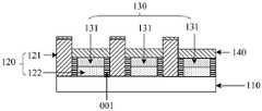
图1是本发明实施例提供的一种显示基板的结构示意图。如图1所示,该显示基板可以包括:衬底基板110,以及设置在衬底基板110上的第一电极层120。该第一电极层120可以包括多个搭接电极121以及多个第一电极122。其中,该多个第一电极122可以由氧化铟锡氧化铟锡(Indium tin oxide,ITO)材料制成,该多个搭接电极121可以由ITO或者银等材料制成。该第一电极122可以为阳极。FIG. 1 is a schematic structural diagram of a display substrate provided by an embodiment of the present invention. As shown in FIG. 1 , the display substrate may include: a
该多个搭接电极121间隔设置在衬底基板110的感光区域,该感光区域可以为用于供传感器感光的区域,每个搭接电极121与驱动电路(图1未示出)连接。该衬底基板110未设置膜层的一侧可以设置有传感器,该传感器在衬底基板110上的正投影可以位于该感光区域区域内。示例的,该传感器可以为摄像头和红外传感器等需要感光的传感器。The plurality of
第一电极层120远离衬底基板110的一侧设置有发光层130,该发光层130位于感光区域的部分可以包括多个间隔设置的发光单元131,且每个搭接电极121的顶部凸出于发光层130。其中,搭接电极121的顶部可以是指该搭接电极121远离衬底基板110的一端。可选的,该发光层130可以由有机发光材料制成。在本发明实施例中,该多个发光单元131形成于像素限定层001所限定的区域内。A light-emitting
发光层130远离衬底基板110的一侧设置有第二电极层140,该第二电极层140位于感光区域的部分可以包括多个间隔设置的第二电极,每个第二电极可以与一个搭接电极121凸出于发光层130的部分的侧壁连接。且每个第二电极在衬底基板110上的正投影与至少一个发光单元131在衬底基板110上的正投影重叠。示例的,该第二电极可以为阴极。A
该搭接电极121可以将驱动电路提供的电源信号传输至对应的第二电极。该第二电极进而可以与每个第一电极122共同驱动发光单元131发光。The overlapping
综上所述,本发明实施例提供了一种显示基板,该显示基板包括衬底基板,以及依次在衬底基板上层叠设置的第一电极层,发光层和第二电极层。该第二电极层位于感光区域的部分包括多个间隔设置的第二电极,每个第二电极与一个搭接电极凸出于发光层的部分的侧壁连接,由此通过该搭接电极将驱动电路提供的电源信号传输至对应的第二电极,该第二电极进而可以与每个第一电极共同驱动发光单元正常发光。本发明实施例提供的显示基板可以通过多个搭接电极为间隔设置的第二电极传输电源信号,确保了第二电极对发光单元的正常驱动。并且,由于该多个第二电极之间存在间隙,因此有效提高了显示基板感光区域的透过率,提高了传感器的感光效果。To sum up, an embodiment of the present invention provides a display substrate, the display substrate includes a base substrate, and a first electrode layer, a light-emitting layer and a second electrode layer stacked on the base substrate in sequence. The part of the second electrode layer located in the photosensitive region includes a plurality of second electrodes arranged at intervals, and each second electrode is connected to a sidewall of a portion of the overlap electrode protruding from the light-emitting layer, so that the overlap electrode is used to connect the The power signal provided by the driving circuit is transmitted to the corresponding second electrode, and the second electrode can then jointly drive the light-emitting unit to emit light normally with each of the first electrodes. The display substrate provided by the embodiment of the present invention can transmit power signals through the second electrodes arranged at intervals by a plurality of overlapping electrodes, so as to ensure the normal driving of the light emitting unit by the second electrodes. In addition, since there are gaps between the plurality of second electrodes, the transmittance of the photosensitive region of the display substrate is effectively improved, and the photosensitive effect of the sensor is improved.
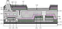
图2是本发明实施例提供的另一种显示基板的局部结构示意图。参考图2,该显示基板还可以包括:间隔设置在感光区域的多个支撑柱150,该多个支撑柱150与多个搭接电极121一一对应。图2中仅示意性的示出了位于衬底基板感光区域的一个支撑柱150和一个搭接电极121。FIG. 2 is a schematic partial structure diagram of another display substrate provided by an embodiment of the present invention. Referring to FIG. 2 , the display substrate may further include: a plurality of
参考图2,每个搭接电极121覆盖在对应的一个支撑柱150远离衬底基板110的一侧,且搭接电极121的顶部与衬底基板110之间的距离,大于发光层130与衬底基板110之间的距离。Referring to FIG. 2 , each
可选的,该发光层130远离衬底基板110的一侧还可以设置有电子传输层132,发光层130靠近衬底基板的一侧设置有空穴传输层133。在制造显示基板的过程中,电子传输层132、空穴传输层133以及第二电极层140会覆盖在搭接电极121的顶部,并覆盖该搭接电极121的部分侧壁。该搭接电极121侧壁上未被其他膜层覆盖的区域与对应的一个第二电极连接。其中,该电子传输层132、空穴注入层133、空穴传输层134可以由有机材料制成。Optionally, an
在本发明实施例中,该多个支撑柱150与平坦层160可以为一体结构。在制造该显示基板的过程中,该多个支撑柱150可以与平坦层160可以通过一次构图工艺形成。或者,也可以先在衬底基板110上形成平坦层160,之后在平坦层160远离衬底基板110的一侧形成该多个支撑柱150。可选的,形成该多个支撑柱150的材料与形成该平坦层160的材料可以为树脂材料。In the embodiment of the present invention, the plurality of
如图2所示,该支撑柱150的侧壁的内侧与平坦层160远离衬底基板110的一面的夹角θ可以为锐角。示例的,该夹角θ的范围可以为5度至85度。As shown in FIG. 2 , the included angle θ between the inner side of the side wall of the
可选的,该支撑柱150可以为圆柱形或多边柱形,例如可以为四边柱形、六边柱形或者八边柱形。Optionally, the
图3示出了第二电极与发光单元以及搭接电极的俯视图。如图3所示,该多个发光单元可以包括红色发光单元R、绿色发光单元G和蓝色发光单元B,且该多个发光单元之间可以设置有透明发光单元002,或者也可以不设置透明发光单元。每个发光单元与一个第一电极122以及一个第二电极141可以组成一个有机发光二极管(Oxide Light EmittingDiode,OLED)或有源矩阵有机发光二极管(Active-matrix Organic Light EmittingDiode,AMOLED)。FIG. 3 shows a top view of the second electrode, the light emitting unit and the overlapping electrode. As shown in FIG. 3 , the plurality of light-emitting units may include a red light-emitting unit R, a green light-emitting unit G, and a blue light-emitting unit B, and a transparent light-emitting
相关技术中,在采用掩膜版蒸镀形成发光层130的过程中,由于掩膜版与发光层130之间的距离较近,可能对发光层130造成损伤。在本发明实施例中,通过设置多个支撑柱,可以代替显示基板中原有的支撑结构,从而起到支撑封装玻璃的作用。同时由于设置有多个凸出于发光层130的支撑柱,在采用掩膜版蒸镀形成发光层130的过程中,可以避免掩膜版与发光层130之间的距离过近,进而可以避免蒸镀过程中对显示基板和发光层130造成损伤的问题。In the related art, in the process of forming the light-emitting
可选的,发光层130位于非感光区域的部分也可以包括多个发光单元131,且位于感光区域的发光单元131的尺寸小于位于非感光区域的发光单元131的尺寸。由于位于感光区域的多个发光单元之间的间距较大,因而提高了显示基板感光区域的透过率,相应的,提高了显示基板下方的传感器的感光效果。其中。该非感光区域指的是在衬底基板的显示区域中,除该感光区域之外的区域。Optionally, the portion of the light-emitting
在本发明实施例中,第二电极层140位于非感光区域的部分可以包括一个片状电极,该片状电极在衬底基板110上的正投影,与非感光区域内的每个发光单元131在衬底基板110上的正投影均重叠。该片状电极与位于非感光区域的每个第一电极122共同驱动非感光区域内的发光单元131发光。In this embodiment of the present invention, the portion of the
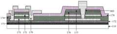
在本发明实施例中,如图2所示,该显示基板还可以包括在衬底基板110上依次层叠设置的聚酰亚胺(Polyimide,PI)膜171、缓冲层172、有源层173、第一绝缘层174、第一栅极层175、第二绝缘层176、第二栅极层177、层间界定层178以及源漏极层179。其中,第二栅极层177可以通过过孔003与源漏极层179连接。其中,源漏极层179可以通过过孔003与有源层173连接。In the embodiment of the present invention, as shown in FIG. 2 , the display substrate may further include a polyimide (PI)
综上所述,本发明实施例提供的一种显示基板,该显示基板包括衬底基板,依次在衬底基板上层叠设置的第一电极层,发光层以及第二电极层。该第二电极层位于感光区域的部分包括多个间隔设置的第二电极,每个第二电极与一个搭接电极凸出于发光层的部分的侧壁连接,由此通过该搭接电极将驱动电路提供的电源信号传输至对应的第二电极,该第二电极进而可以与每个第一电极共同驱动发光单元正常发光。本发明实施例提供的显示基板可以通过多个搭接电极为间隔设置的第二电极传输电源信号,确保了第二电极对发光单元的正常驱动。并且,由于该多个第二电极之间存在间隙,因此有效提高了显示基板感光区域的透过率,提高了传感器的感光效果。To sum up, an embodiment of the present invention provides a display substrate, the display substrate includes a base substrate, a first electrode layer, a light-emitting layer and a second electrode layer stacked on the base substrate in sequence. The part of the second electrode layer located in the photosensitive region includes a plurality of second electrodes arranged at intervals, and each second electrode is connected to a sidewall of a portion of the overlap electrode protruding from the light-emitting layer, so that the overlap electrode is used to connect the The power signal provided by the driving circuit is transmitted to the corresponding second electrode, and the second electrode can then jointly drive the light-emitting unit to emit light normally with each of the first electrodes. The display substrate provided by the embodiment of the present invention can transmit power signals through the second electrodes arranged at intervals by a plurality of overlapping electrodes, so as to ensure the normal driving of the light emitting unit by the second electrodes. In addition, since there are gaps between the plurality of second electrodes, the transmittance of the photosensitive region of the display substrate is effectively improved, and the photosensitive effect of the sensor is improved.
图4是本发明实施例提供的一种显示基板的制造方法的流程图。该方法可以用于制造如图1所示的显示基板,如图4所示,该方法可以包括:FIG. 4 is a flowchart of a method for manufacturing a display substrate according to an embodiment of the present invention. The method can be used to manufacture the display substrate shown in FIG. 1 , and as shown in FIG. 4 , the method can include:
步骤201、在衬底基板上形成第一电极层,该第一电极层包括多个搭接电极以及多个第一电极,该多个搭接电极间隔形成在衬底基板的感光区域,该感光区域为用于供传感器感光的区域,该每个搭接电极与驱动电路连接。
在本发明实施例中,该多个搭接电极121以及多个第一电极122可以通过一次构图工艺形成。或者,也可以采用多次构图工艺在衬底基板110上形成多个第一电极122和该多个搭接电极121。该多个第一电极122可以由ITO材料制成,该多个搭接电极121可以由ITO或者银等材料制成。该第一电极122可以为阳极。In the embodiment of the present invention, the plurality of
该衬底基板110未设置膜层的一侧可以设置有传感器,该传感器在衬底基板110上的正投影位于该感光区域区域内。示例的,该传感器可以为摄像头和红外传感器等需要感光的传感器。该形成有第一电极层120的衬底基板110的示意图可以参考图5。The side of the
步骤202、在第一电极层远离衬底基板的一侧形成发光层,该发光层位于感光区域的部分包括多个间隔形成的发光单元,且每个搭接电极的顶部凸出于发光层。
该发光层可以由有机发光材料制成。在本发明实施例中,该多个发光单元131形成于像素限定层001所限定的区域内。该形成发光层的衬底基板110的示意图可以参考图6。The light-emitting layer may be made of organic light-emitting materials. In the embodiment of the present invention, the plurality of light emitting
步骤203、在发光层远离衬底基板的一侧形成第二电极层,该第二电极层位于感光区域的部分包括多个间隔形成的第二电极,每个第二电极与一个搭接电极凸出于发光层的部分的侧壁连接,且每个第二电极在衬底基板上的正投影与至少一个发光单元在衬底基板上的正投影重叠。
该搭接电极121可以将驱动电路提供的电源信号传输至对应的第二电极。该第二电极进而可以与每个第一电极122共同驱动发光单元131发光。示例的,该第二电极可以为阴极。该形成有第二电极层140的衬底基板110的示意图可以参考图1。The overlapping
综上所述,本发明实施例提供的一种显示基板的制造方法,在衬底基板上形成第一电极层,在第一电极层远离衬底基板的一侧形成发光层,在发光层远离衬底基板的一侧形成第二电极层。该第二电极层位于感光区域的部分包括多个间隔设置的第二电极,每个第二电极与一个搭接电极凸出于发光层的部分的侧壁连接,由此通过该搭接电极将驱动电路提供的电源信号传输至对应的第二电极,该第二电极进而可以与每个第一电极共同驱动发光单元正常发光。本发明实施例提供的显示基板可以通过多个搭接电极为间隔设置的第二电极传输电源信号,确保了第二电极对发光单元的正常驱动。并且,由于该多个第二电极之间存在间隙,因此有效提高了显示基板感光区域的透过率,提高了传感器的感光效果。To sum up, a method for manufacturing a display substrate provided by an embodiment of the present invention includes forming a first electrode layer on a base substrate, forming a light-emitting layer on the side of the first electrode layer away from the base substrate, and forming a light-emitting layer on the side of the first electrode layer away from the base substrate. A second electrode layer is formed on one side of the base substrate. The part of the second electrode layer located in the photosensitive region includes a plurality of second electrodes arranged at intervals, and each second electrode is connected to a sidewall of a portion of the overlap electrode protruding from the light-emitting layer, so that the overlap electrode is used to connect the The power signal provided by the driving circuit is transmitted to the corresponding second electrode, and the second electrode can then jointly drive the light-emitting unit to emit light normally with each of the first electrodes. The display substrate provided by the embodiment of the present invention can transmit power signals through the second electrodes arranged at intervals by a plurality of overlapping electrodes, so as to ensure the normal driving of the light emitting unit by the second electrodes. In addition, since there are gaps between the plurality of second electrodes, the transmittance of the photosensitive region of the display substrate is effectively improved, and the photosensitive effect of the sensor is improved.
图7是本发明实施例提供的一种显示基板的制造方法的流程图。该方法可以用于制造如图1或图2所示的显示基板,如图7所示,该方法可以包括:FIG. 7 is a flowchart of a method for manufacturing a display substrate according to an embodiment of the present invention. The method can be used to manufacture the display substrate shown in FIG. 1 or FIG. 2 , and as shown in FIG. 7 , the method can include:
步骤301、在衬底基板的感光区域间隔形成多个支撑柱。
在本发明实施例中,可以采用一次构图工艺在衬底基板110的感光区域间隔形成该多个支撑柱150。其中,该一次构图工艺可以包括:沉积膜层、光刻胶涂覆、曝光、显影、刻蚀和光刻胶剥离等步骤。In the embodiment of the present invention, the plurality of
本发明实施例中,该支撑柱150与平坦层160可以为一体结构。该多个支撑柱150可以与平坦层160通过一次构图工艺形成。或者,也可以先在衬底基板110上形成平坦层160,之后在平坦层160远离衬底基板110的一侧形成该多个支撑柱150,本发明实施例对此不做限定。可选的,且形成该多个支撑柱150的材料与形成该平坦层160的材料可以为树脂材料。In the embodiment of the present invention, the
该支撑柱150的侧壁的内侧与平坦层160远离衬底基板110的一面的夹角θ可以为锐角。示例的,该夹角θ的范围可以为5度至85度。The included angle θ between the inner side of the side wall of the
可选的,该支撑柱150的形状可以为带有夹角的圆柱形或多边柱形,例如可以为四边柱形、六边柱形或者八边柱形。Optionally, the shape of the
在本发明实施例中,在衬底基板110的感光区域间隔形成多个支撑柱150之前,还可以在衬底基板110上依次形成PI膜171、缓冲层172、有源层173、第一绝缘层174、第一栅极层175、第二绝缘层176、第二栅极层177、层间介质层178以及源漏极层179。示例的,形成缓冲层172的材料可以为氮化硅。形成该有源层173的材料可以为P型硅(P-si)。形成第一栅极层175、第二栅极层177以及源漏极层179的材料可以为导电材料。其中,源漏极层179可以通过过孔003与有源层173连接。该形成有PI膜171、缓冲层172、有源层173、第一绝缘层174、第一栅极层175、第二绝缘层176、第二栅极层177、层间介质层178以及源漏极层179的衬底基板110的示意图可以参考图8。该形成有平坦层160和支撑柱150的衬底基板110的示意图可以参考图9。In the embodiment of the present invention, before a plurality of supporting
步骤302、在衬底基板上形成第一电极层。
在本发明实施例中,可以采用构图工艺在衬底基板110上形成第一电极层120。该第一电极层可以包括多个搭接电极121以及多个第一电极122,该多个搭接电极121间隔形成在衬底基板110的感光区域,该感光区域为用于供传感器感光的区域,每个搭接电极121与驱动电路连接。In this embodiment of the present invention, a patterning process may be used to form the
可选的,步骤302可以包括:Optionally,
在每个支撑柱150远离衬底基板110的一侧形成覆盖在支撑柱150上的一个搭接电极121。A
在本发明实施例中,通过设置该多个支撑柱,可以代替显示基板中原有的支撑结构,从而起到支撑封装玻璃作用,同时由于设置有多个凸出于发光层的支撑柱,在采用掩膜版蒸镀形成发光层的过程中,可以避免掩膜版与发光层之间的距离过近,进而可以避免蒸镀过程对显示基板和发光层造成损伤的问题。该形成有第一电极层120的衬底基板110的示意图可以参考图10。In the embodiment of the present invention, by disposing the plurality of support columns, the original support structure in the display substrate can be replaced, so as to support the encapsulation glass. In the process of evaporating the mask to form the light-emitting layer, the distance between the mask and the light-emitting layer can be prevented from being too close, thereby avoiding the problem of damage to the display substrate and the light-emitting layer during the evaporation process. For a schematic diagram of the
步骤303、在第一电极层远离衬底基板的一侧形成发光层。
可选的,可以在第一电极层120远离衬底基板110的一侧形成像素限定层001,之后在形成像素限定层001远离衬底基板110的一侧形成空穴注入层133,并在空穴注入层133远离衬底基板110的一侧形成空穴传输层134,之后,采用蒸镀的方法在像素限定层001远离衬底基板110的一侧形成发光层,最后,在发光层远离衬底基板110的一侧形成电子传输层132。该发光层位于感光区域的部分可以包括多个间隔设置的发光单元131,且每个搭接电极121的顶部凸出于发光层。Optionally, the
该多个发光单元131之间可以设置有透明发光单元002,或者也可以不设置透明发光单元。示例的,该发光层可以由有机材料制成。A transparent light-emitting
在本发明实施例中,搭接电极121的顶部与衬底基板110之间的距离,大于发光层与衬底基板110之间的距离。该形成有发光层的衬底基板110的示意图可以参考图11。In the embodiment of the present invention, the distance between the top of the
步骤304、在发光层远离衬底基板的一侧形成第二电极层。
可选的,可以采用精密金属掩膜版(FineMetalMask)对发光层远离衬底基板110的一侧进行蒸镀,以形成第二电极层140。该第二电极层140位于感光区域的部分可以包括多个间隔形成的第二电极,每个第二电极与一个搭接电极121凸出于发光层的部分的侧壁连接,且每个第二电极在衬底基板110上的正投影与至少一个发光单元131在衬底基板110上的正投影重叠。Optionally, a fine metal mask may be used to evaporate the light emitting layer on the side away from the
该搭接电极121可以将驱动电路提供的电源信号传输至对应的第二电极。该第二电极进而可以与每个第一电极122共同驱动发光单元131发光。该形成有位于感光区域的第二电极层140的衬底基板110的示意图可以参考图2。The overlapping
需要说明的是,本发明实施例提供的显示基板的制造方法的步骤的先后顺序可以进行适当调整,步骤也可以根据情况进行相应增减。任何熟悉本技术领域的技术人员在本发明揭露的技术范围内,可轻易想到变化的方法,都应涵盖在本发明的保护范围之内,因此不再赘述。It should be noted that, the order of the steps of the method for manufacturing the display substrate provided by the embodiment of the present invention can be adjusted appropriately, and the steps can also be increased or decreased according to the situation. Any person skilled in the art who is familiar with the technical scope of the present invention can easily think of any variation of the method, which should be included in the protection scope of the present invention, and therefore will not be repeated.
综上所述,本发明实施例提供的一种显示基板的制造方法,在衬底基板上形成第一电极层,在第一电极层远离衬底基板的一侧形成发光层,在发光层远离衬底基板的一侧形成第二电极层。该第二电极层位于感光区域的部分包括多个间隔设置的第二电极,每个第二电极与一个搭接电极凸出于发光层的部分的侧壁连接,由此通过该搭接电极将驱动电路提供的电源信号传输至对应的第二电极,该第二电极进而可以与每个第一电极共同驱动发光单元正常发光。本发明实施例提供的显示基板可以通过多个搭接电极为间隔设置的第二电极传输电源信号,确保了第二电极对发光单元的正常驱动。并且,由于该多个第二电极之间存在间隙,因此有效提高了显示基板感光区域的透过率,提高了传感器的感光效果。To sum up, a method for manufacturing a display substrate provided by an embodiment of the present invention includes forming a first electrode layer on a base substrate, forming a light-emitting layer on the side of the first electrode layer away from the base substrate, and forming a light-emitting layer on the side of the first electrode layer away from the base substrate. A second electrode layer is formed on one side of the base substrate. The part of the second electrode layer located in the photosensitive region includes a plurality of second electrodes arranged at intervals, and each second electrode is connected to a sidewall of a portion of the overlap electrode protruding from the light-emitting layer, so that the overlap electrode is used to connect the The power signal provided by the driving circuit is transmitted to the corresponding second electrode, and the second electrode can then jointly drive the light-emitting unit to emit light normally with each of the first electrodes. The display substrate provided by the embodiment of the present invention can transmit power signals through the second electrodes arranged at intervals by a plurality of overlapping electrodes, so as to ensure the normal driving of the light emitting unit by the second electrodes. In addition, since there are gaps between the plurality of second electrodes, the transmittance of the photosensitive region of the display substrate is effectively improved, and the photosensitive effect of the sensor is improved.
本发明实施例提供了一种显示装置,该显示装置包括如图1或图2所示的显示基板。该显示装置可以为:电子纸、手机、平板电脑、电视机、显示器、笔记本电脑、数码相框、导航仪等任何具有显示功能的产品或部件。An embodiment of the present invention provides a display device, and the display device includes a display substrate as shown in FIG. 1 or FIG. 2 . The display device can be any product or component with display function, such as electronic paper, mobile phone, tablet computer, TV, monitor, notebook computer, digital photo frame, and navigator.
以上所述仅为本发明的较佳实施例,并不用以限制本发明,凡在本发明的精神和原则之内,所作的任何修改、等同替换、改进等,均应包含在本发明的保护范围之内。The above are only preferred embodiments of the present invention and are not intended to limit the present invention. Any modifications, equivalent replacements, improvements, etc. made within the spirit and principles of the present invention shall be included in the protection of the present invention. within the range.
Claims (10)
Translated fromChinesePriority Applications (2)
| Application Number | Priority Date | Filing Date | Title |
|---|---|---|---|
| CN201811027575.7ACN109119451B (en) | 2018-09-04 | 2018-09-04 | Display substrate, method for manufacturing the same, and display device |
| US16/451,136US11257868B2 (en) | 2018-09-04 | 2019-06-25 | Display substrate, fabricating method thereof and display device |
Applications Claiming Priority (1)
| Application Number | Priority Date | Filing Date | Title |
|---|---|---|---|
| CN201811027575.7ACN109119451B (en) | 2018-09-04 | 2018-09-04 | Display substrate, method for manufacturing the same, and display device |
Publications (2)
| Publication Number | Publication Date |
|---|---|
| CN109119451A CN109119451A (en) | 2019-01-01 |
| CN109119451Btrue CN109119451B (en) | 2020-08-25 |
Family
ID=64861972
Family Applications (1)
| Application Number | Title | Priority Date | Filing Date |
|---|---|---|---|
| CN201811027575.7AActiveCN109119451B (en) | 2018-09-04 | 2018-09-04 | Display substrate, method for manufacturing the same, and display device |
Country Status (2)
| Country | Link |
|---|---|
| US (1) | US11257868B2 (en) |
| CN (1) | CN109119451B (en) |
Families Citing this family (7)
| Publication number | Priority date | Publication date | Assignee | Title |
|---|---|---|---|---|
| CN111987120B (en)* | 2019-05-24 | 2025-07-11 | 北京小米移动软件有限公司 | Pixel display component, screen display component, display screen and terminal |
| KR20200136549A (en) | 2019-05-27 | 2020-12-08 | 삼성디스플레이 주식회사 | Display apparatus and Method of manufacturing of the same |
| CN110767725B (en)* | 2019-10-29 | 2022-05-10 | 维沃移动通信有限公司 | Display substrate, display device and manufacturing method of display substrate |
| CN113345929B (en)* | 2020-02-18 | 2023-07-18 | 京东方科技集团股份有限公司 | Display substrate, manufacturing method thereof, and display device |
| CN113838888B (en)* | 2020-06-23 | 2024-10-22 | 京东方科技集团股份有限公司 | Display substrate and display device |
| CN111864111B (en)* | 2020-07-17 | 2022-08-05 | 武汉华星光电半导体显示技术有限公司 | Display panel |
| CN115101567B (en)* | 2022-06-28 | 2025-06-20 | 武汉天马微电子有限公司 | Display panel and display device |
Citations (4)
| Publication number | Priority date | Publication date | Assignee | Title |
|---|---|---|---|---|
| CN102479798A (en)* | 2010-11-25 | 2012-05-30 | 三星移动显示器株式会社 | Organic light emitting display device and method for manufacturing the same |
| CN103426900A (en)* | 2012-05-16 | 2013-12-04 | 三星显示有限公司 | Organic light-emitting display apparatus and method of manufacturing the same |
| CN103700687A (en)* | 2013-12-20 | 2014-04-02 | 京东方科技集团股份有限公司 | Organic light-emitting display panel and manufacturing method thereof as well as display device |
| CN207165572U (en)* | 2017-09-12 | 2018-03-30 | 京东方科技集团股份有限公司 | A kind of array base palte and display device |
Family Cites Families (12)
| Publication number | Priority date | Publication date | Assignee | Title |
|---|---|---|---|---|
| KR101073552B1 (en)* | 2009-10-09 | 2011-10-17 | 삼성모바일디스플레이주식회사 | Organic light emitting diode display and method of manufacturing the same |
| KR101811702B1 (en)* | 2010-10-27 | 2017-12-26 | 삼성디스플레이 주식회사 | Organinc light emitting display device and manufacturing method for the same |
| US20150187830A1 (en)* | 2013-12-31 | 2015-07-02 | Shenzhen China Star Optoelectronics Technology Co., Ltd. | Photosensitive unit, array substrate of display panel and manufacturing method thereof |
| KR102265752B1 (en)* | 2014-09-01 | 2021-06-17 | 삼성디스플레이 주식회사 | organic light emitting diode display |
| KR20170013661A (en)* | 2015-07-28 | 2017-02-07 | 엘지디스플레이 주식회사 | Organic light emitting diode display and manufacturing method of the same |
| US10644077B1 (en)* | 2015-10-28 | 2020-05-05 | Apple Inc. | Display with array of light-transmitting windows |
| CN107608549B (en)* | 2017-09-08 | 2020-08-25 | 京东方科技集团股份有限公司 | Induction panel, display device and driving method thereof |
| KR102480091B1 (en)* | 2018-01-30 | 2022-12-23 | 삼성디스플레이 주식회사 | display device |
| US20190245011A1 (en)* | 2018-02-06 | 2019-08-08 | Innolux Corporation | Display device |
| DE102018103603A1 (en)* | 2018-02-19 | 2019-08-22 | Osram Opto Semiconductors Gmbh | display device |
| KR102509439B1 (en)* | 2018-03-06 | 2023-03-13 | 삼성디스플레이 주식회사 | Fingerprint sensor package and display device including the same |
| KR102792464B1 (en)* | 2019-01-10 | 2025-04-07 | 삼성디스플레이 주식회사 | Display device |
- 2018
- 2018-09-04CNCN201811027575.7Apatent/CN109119451B/enactiveActive
- 2019
- 2019-06-25USUS16/451,136patent/US11257868B2/enactiveActive
Patent Citations (4)
| Publication number | Priority date | Publication date | Assignee | Title |
|---|---|---|---|---|
| CN102479798A (en)* | 2010-11-25 | 2012-05-30 | 三星移动显示器株式会社 | Organic light emitting display device and method for manufacturing the same |
| CN103426900A (en)* | 2012-05-16 | 2013-12-04 | 三星显示有限公司 | Organic light-emitting display apparatus and method of manufacturing the same |
| CN103700687A (en)* | 2013-12-20 | 2014-04-02 | 京东方科技集团股份有限公司 | Organic light-emitting display panel and manufacturing method thereof as well as display device |
| CN207165572U (en)* | 2017-09-12 | 2018-03-30 | 京东方科技集团股份有限公司 | A kind of array base palte and display device |
Also Published As
| Publication number | Publication date |
|---|---|
| US11257868B2 (en) | 2022-02-22 |
| CN109119451A (en) | 2019-01-01 |
| US20200075688A1 (en) | 2020-03-05 |
Similar Documents
| Publication | Publication Date | Title |
|---|---|---|
| CN109119451B (en) | Display substrate, method for manufacturing the same, and display device | |
| CN109103231B (en) | Display substrate, method for manufacturing the same, and display device | |
| CN106992204B (en) | OLED array substrate, preparation method thereof and display device | |
| US9761641B2 (en) | Color filter substrate and method for manufacturing the same, OLED display panel and display apparatus | |
| US10205121B2 (en) | Organic electroluminescent display panel and display apparatus | |
| WO2020192585A1 (en) | Array substrate and preparation method therefor, display panel, display device and pixel drive circuit | |
| CN111081732A (en) | display device | |
| CN109728060B (en) | Array substrate, electroluminescent panel and display device | |
| US10418421B2 (en) | Silicon-based OLED image transceiving device and manufacture method thereof | |
| WO2019233267A1 (en) | Thin film transistor and manufacturing method and display device | |
| US11563064B2 (en) | Array substrate, display device, and method for fabricating an array substrate | |
| WO2016107311A1 (en) | Amoled array substrate, method for manufacturing amoled array substrate, and display device | |
| WO2016101576A1 (en) | Array substrate and manufacturing method therefor, and display device | |
| WO2021164602A1 (en) | Display substrate, manufacturing method therefor, and display device | |
| WO2019242600A1 (en) | Organic electroluminescent display panel, fabrication method therefor, and display apparatus | |
| WO2018171268A1 (en) | Substrate and preparation method therefor, display panel and display device | |
| WO2020224487A1 (en) | Cover board structure and manufacture method therefor, display panel and display device | |
| CN110752220B (en) | Display substrate, preparation method thereof and display panel | |
| CN112068732B (en) | Display panel and display device | |
| WO2020001020A1 (en) | Display substrate, preparation method therefor, and display device | |
| CN110148618B (en) | Display substrate, manufacturing method thereof and display device | |
| WO2020087858A1 (en) | Display panel, display terminal and mask plate | |
| KR20240161888A (en) | Display device and method of fabricating the same | |
| CN113035901B (en) | Light-transmitting display panel, preparation method thereof and display panel | |
| CN111916578A (en) | Array substrate, preparation method thereof and display device |
Legal Events
| Date | Code | Title | Description |
|---|---|---|---|
| PB01 | Publication | ||
| PB01 | Publication | ||
| SE01 | Entry into force of request for substantive examination | ||
| SE01 | Entry into force of request for substantive examination | ||
| GR01 | Patent grant | ||
| GR01 | Patent grant |