CN109103552B - Loaded lumped element frequency selective surface - Google Patents
Loaded lumped element frequency selective surfaceDownload PDFInfo
- Publication number
- CN109103552B CN109103552BCN201810747997.5ACN201810747997ACN109103552BCN 109103552 BCN109103552 BCN 109103552BCN 201810747997 ACN201810747997 ACN 201810747997ACN 109103552 BCN109103552 BCN 109103552B
- Authority
- CN
- China
- Prior art keywords
- shaped metal
- frequency
- lumped
- outer ring
- gap
- Prior art date
- Legal status (The legal status is an assumption and is not a legal conclusion. Google has not performed a legal analysis and makes no representation as to the accuracy of the status listed.)
- Active
Links
- 239000002184metalSubstances0.000claimsabstractdescription87
- 239000000758substrateSubstances0.000claimsabstractdescription15
- 239000003990capacitorSubstances0.000claimsabstractdescription5
- 230000009977dual effectEffects0.000claimsdescription2
- 230000035699permeabilityEffects0.000claimsdescription2
- 238000000034methodMethods0.000description3
- 238000010586diagramMethods0.000description2
- 230000000694effectsEffects0.000description2
- 230000000737periodic effectEffects0.000description2
- 238000004088simulationMethods0.000description2
- 238000005452bendingMethods0.000description1
- 230000005540biological transmissionEffects0.000description1
- 238000004891communicationMethods0.000description1
- 230000000295complement effectEffects0.000description1
- 238000012938design processMethods0.000description1
- 230000005855radiationEffects0.000description1
Images


Classifications
- H—ELECTRICITY
- H01—ELECTRIC ELEMENTS
- H01P—WAVEGUIDES; RESONATORS, LINES, OR OTHER DEVICES OF THE WAVEGUIDE TYPE
- H01P1/00—Auxiliary devices
- H01P1/20—Frequency-selective devices, e.g. filters
Landscapes
- Control Of Motors That Do Not Use Commutators (AREA)
- Circuit Arrangements For Discharge Lamps (AREA)
Abstract
Description
Translated fromChinese技术领域technical field
本发明属于无线通信FSS技术领域,特别是一种加载集总元件频率选择表面。The invention belongs to the technical field of wireless communication FSS, in particular to a load lumped element frequency selective surface.
背景技术Background technique
传统小型化的实现方式主要有弯折结构加载,集总元件加载等方式。The traditional miniaturization methods mainly include bending structure loading and lumped element loading.
目前,FSS在小型化,多频带和低剖面等方面都有重大进展。FSS的实现方案主要有金属加载,其周期单元大致可分为两种类型,一种是金属贴片,另一种是与之互补的在金属平板上开槽缝隙结构。At present, FSS has made significant progress in miniaturization, multi-band and low profile. The implementation scheme of FSS mainly includes metal loading, and its periodic unit can be roughly divided into two types, one is a metal patch, and the other is a complementary slotted slot structure on a metal plate.
频率选择表面本身不吸收能量,它的响应特性随频率而变化,对某些频带内的入射电磁波几乎全透明,而对另一些频带内的入射波则呈现接近全反射的特性。其频率特性主要取决于谐振单元的结构、周期性排列方式以及加载的介质。当频率选择表面的谐振单元达到谐振状态时,处于谐振频率的电磁波被全反射贴片型或全透射缝隙型。由于低频段频率选择表面谐振频率接近,且电尺寸大,因此实现难度很大,The frequency selective surface itself does not absorb energy, and its response characteristics vary with frequency. It is almost completely transparent to incident electromagnetic waves in some frequency bands, while it exhibits near total reflection characteristics to incident waves in other frequency bands. Its frequency characteristic mainly depends on the structure of the resonance unit, the periodic arrangement and the loaded medium. When the resonance unit of the frequency selective surface reaches the resonance state, the electromagnetic wave at the resonance frequency is totally reflected by the patch type or the totally transmitted slot type. Due to the close resonant frequency of the low-frequency frequency selection surface and the large electrical size, it is very difficult to realize.
发明内容SUMMARY OF THE INVENTION
本发明的目的在于提供一种加载集总元件频率选择表面,同时实现小型化和双频段。The purpose of the present invention is to provide a load lumped element frequency selective surface that simultaneously achieves miniaturization and dual frequency bands.
实现本发明目的的技术方案为:一种加载集总元件频率选择表面,包括介质基板和紧贴于介质基板上表面的内环金属贴片、外环金属贴片;The technical scheme for realizing the object of the present invention is: a frequency selection surface for loading lumped elements, which includes a dielectric substrate, an inner ring metal patch and an outer ring metal patch closely attached to the upper surface of the dielectric substrate;
内环金属贴片包括四片第一L型金属贴片,每个第一L型金属贴片的两条边垂直且边长相等,相邻两个第一L型金属贴片留有间隙,每个间隙设置有一个第一集总电感;四个第一L型金属贴片围成正方形金属环;The inner ring metal patch includes four first L-shaped metal patches, the two sides of each first L-shaped metal patch are vertical and the side lengths are equal, and there is a gap between the adjacent two first L-shaped metal patches, Each gap is provided with a first lumped inductance; four first L-shaped metal patches form a square metal ring;
外环金属贴片包括四片第二L型金属贴片,每个第二L型金属贴片的两条边垂直且边长相等,相邻两个第二L型金属贴片留有间隙,其中两个相邻的间隙设置有集总电容,另外两个相邻的间隙设置有第二集总电感,四个第二L型金属贴片围成正方形金属环。The outer ring metal patch includes four second L-shaped metal patches, the two sides of each second L-shaped metal patch are vertical and the side lengths are equal, and there is a gap between two adjacent second L-shaped metal patches. Two adjacent gaps are provided with lumped capacitors, and the other two adjacent gaps are provided with second lumped inductances, and four second L-shaped metal patches surround a square metal ring.
本发明与现有技术相比,其显著优点为:(1)本发明金属结构的尺寸可以根据设计的频率和选取板材的介电常数快速计算出来,设计过程简单;(2)通过加载集总元件的方法能够为频率选择表面引入新的自由度,方便双频FSS的设计,为FSS在低频段应用提供了完美的解决方案,相比于金属加载,本发明采用的集总元件加载结构可大大提升FSS的小型化指标;(3)本发明可以用集总元件来实现更高的小型化指标和更灵活的谐振频点设计,从而拓宽了谐振频率的设计范围。Compared with the prior art, the present invention has the following significant advantages: (1) the size of the metal structure of the present invention can be quickly calculated according to the designed frequency and the dielectric constant of the selected plate, and the design process is simple; (2) by loading lumped The element method can introduce a new degree of freedom for the frequency selective surface, facilitate the design of dual-frequency FSS, and provide a perfect solution for FSS in low-frequency applications. Compared with metal loading, the lumped element loading structure used in the present invention can be used. The miniaturization index of FSS is greatly improved; (3) the present invention can use lumped elements to achieve higher miniaturization index and more flexible resonance frequency design, thereby broadening the design range of resonance frequency.
附图说明Description of drawings
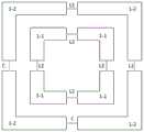
图1是加载集总元件频率选择表面俯视图。Figure 1 is a top view of the loaded lumped element frequency selective surface.
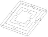
图2是加载集总元件频率选择表面的尺寸图。Figure 2 is a dimensional drawing of the loaded lumped element frequency selective surface.
图3是介质基板的尺寸图。FIG. 3 is a dimension drawing of a dielectric substrate.
图4是双频FSS采用CST仿真的S11图。Figure 4 is the S11 diagram of dual-frequency FSS using CST simulation.
图5是双频FSS采用CST仿真的S21图。Figure 5 is the S21 diagram of dual-frequency FSS using CST simulation.
图6是双频FSS结构的不同角度入射S21传输曲线图。FIG. 6 is a graph showing the S21 transmission curves of the dual-frequency FSS structure at different angles of incidence.
具体实施方式Detailed ways
一种加载集总元件频率选择表面,主要由介质板、金属结构和集总元件组成。金属结构和集总元件加载在介质板表面。介质板表面结构部分是本发明的核心部分,合适地选择金属结构尺寸和集总元件实现FSS在两个频点上的增强效应。A loaded lumped element frequency selective surface consisting mainly of a dielectric plate, a metal structure and lumped elements. Metal structures and lumped elements are loaded on the dielectric plate surface. The surface structure part of the dielectric plate is the core part of the present invention, and the size of the metal structure and the lumped element are appropriately selected to realize the enhancement effect of FSS at two frequency points.
结合图1,一种加载集总元件频率选择表面,包括介质基板2和紧贴于介质基板2上表面的内环金属贴片1-1、外环金属贴片1-2;Referring to FIG. 1 , a loading lumped element frequency selection surface includes a
内环金属贴片1-1包括四片第一L型金属贴片,每个第一L型金属贴片的两条边垂直且边长相等,相邻两个第一L型金属贴片留有间隙,每个间隙设置有一个第一集总电感L2;四个第一L型金属贴片围成正方形金属环;The inner ring metal patch 1-1 includes four first L-shaped metal patches, the two sides of each first L-shaped metal patch are vertical and the side lengths are equal, and two adjacent first L-shaped metal patches remain. There are gaps, and each gap is provided with a first lumped inductance L2; four first L-shaped metal patches surround a square metal ring;
外环金属贴片1-2包括四片第二L型金属贴片,每个第二L型金属贴片的两条边垂直且边长相等,相邻两个第二L型金属贴片留有间隙,其中两个相邻的间隙设置有集总电容C,另外两个相邻的间隙设置有第二集总电感L1,四个第二L型金属贴片围成正方形金属环。The outer ring metal patch 1-2 includes four second L-shaped metal patches, the two sides of each second L-shaped metal patch are vertical and the side lengths are equal, and the adjacent two second L-shaped metal patches are reserved. There are gaps, two adjacent gaps are provided with lumped capacitors C, the other two adjacent gaps are provided with second lumped inductance L1, and four second L-shaped metal patches surround a square metal ring.
相邻两个第一L型金属贴片的间隙大小相同,相邻两个第二L型金属贴片的间隙大小相同。The size of the gap between two adjacent first L-shaped metal patches is the same, and the size of the gap between two adjacent second L-shaped metal patches is the same.
进一步的,第一L型金属贴片和第二L型金属贴片的宽度相同。Further, the widths of the first L-shaped metal patch and the second L-shaped metal patch are the same.
进一步的,介质基板的介电常数为2.2。Further, the dielectric constant of the dielectric substrate is 2.2.
进一步的,内外环之间的缝隙电容为:Further, the gap capacitance between the inner and outer rings is:

式中,ε0为真空中的介电常数,εeff为介质板的有效介电系数,D为外环金属贴片围成正方形的边长,M为内环金属贴片围成正方形的边长,L为第一L型金属贴片和第L型金属贴片的宽度。In the formula, ε0 is the dielectric constant in vacuum, εeff is the effective dielectric coefficient of the dielectric plate, D is the side length of the square surrounded by the outer ring metal patch, M is the side of the square surrounded by the inner ring metal patch Length, L is the width of the first L-shaped metal patch and the L-th metal patch.
下面结合附图和实施例具体说明本发明内容。The content of the present invention will be described in detail below with reference to the accompanying drawings and embodiments.
实施例Example
如图2、图3所示,本发明主要由金属结构、集总元件和介质基板组成,实现两个频率的辐射。该表面满足以下特性:As shown in Figures 2 and 3, the present invention is mainly composed of a metal structure, a lumped element and a dielectric substrate, and realizes radiation of two frequencies. The surface satisfies the following properties:


式中,L内环为结构内环的等效电感,L外环左为结构外环左侧等效电感,L外环右为结构外金属环右侧等效电感。L1、L2为集总电感L1、L2的电感值,εeff为介质板的有效介电系数。μ0为真空中的磁导率,ε0为真空中的介电常数,εr为介质板介电系数,C缝隙为内外环之间的缝隙电容,S为外环金属贴片中相邻两个第二L型金属贴片间隙距离。In the formula, the Linner ring is the equivalent inductance of the inner ring of the structure, theleft of the L outer ring is the equivalent inductance of the left side of the outer ring of the structure, and the right of the Louter ring is the equivalent inductance of the right side of the outer metal ring of the structure. L1 and L2 are the inductance values of the lumped inductances L1 and L2, and εeff is the effective dielectric coefficient of the dielectric plate. μ0 is the magnetic permeability in vacuum, ε0 is the dielectric constant in vacuum, εr is the dielectric coefficient of the dielectric plate, Cgap is the gap capacitance between the inner and outer rings, S is the adjacent metal patch in the outer ring Two second L-shaped metal patch clearance distance.


其中,f1为双频频率选择表面结构的低频谐振频率,f2为高频谐振频率,f1-stop为低频截止频率,f2-stop为高频截止频率,C为外环金属贴片中两个相邻第二L型金属贴片间隙加载的集总电容电容值。Among them, f1 is the low-frequency resonance frequency of the dual-frequency frequency selection surface structure, f2 is the high-frequency resonance frequency, f1-stop is the low-frequency cut-off frequency, f2-stop is the high-frequency cut-off frequency, and C is the outer ring metal patch The capacitance value of the lumped capacitance loaded by the gap between the two adjacent second L-shaped metal patches.
本实施例中两个频率选取2.4GHz和5.25GHz,基板选取介电常数为2.2,厚度h为0.508mm的4003板材。In this embodiment, the two frequencies are 2.4GHz and 5.25GHz, and the substrate is a 4003 plate with a dielectric constant of 2.2 and a thickness h of 0.508mm.
FSS主要尺寸参数如下:The main size parameters of FSS are as follows:
D=10mm,L=1mm,S=0.8mm,M=6mm,h=0.508mm,C=1pF,L1=2nH,L2=5.6nH。D=10mm, L=1mm, S=0.8mm, M=6mm, h=0.508mm, C=1pF, L1=2nH, L2=5.6nH.
图4为设计的FSS在电磁仿真软件CST下仿真的S参数,在2.4G和5.25G两频点,S11都小于-20dB。Figure 4 shows the S parameters simulated by the designed FSS under the electromagnetic simulation software CST. At the two frequency points of 2.4G and 5.25G, S11 is less than -20dB.
图5为设计的FSS在电磁仿真软件CST下仿真的S参数,在2.4G和5.25G两频点,S21都大于-0.1dB。Figure 5 shows the S parameters simulated by the designed FSS under the electromagnetic simulation software CST. At the two frequency points of 2.4G and 5.25G, S21 is greater than -0.1dB.
图6为设计的FSS在电磁仿真软件CST下仿真的角度扫描参数,在2.4G和5.25G两频点,倾斜入射对FSS性能影响不大。Figure 6 shows the angle sweep parameters simulated by the designed FSS under the electromagnetic simulation software CST. At the two frequency points of 2.4G and 5.25G, the oblique incidence has little effect on the performance of the FSS.
Claims (2)


Priority Applications (1)
| Application Number | Priority Date | Filing Date | Title |
|---|---|---|---|
| CN201810747997.5ACN109103552B (en) | 2018-07-10 | 2018-07-10 | Loaded lumped element frequency selective surface |
Applications Claiming Priority (1)
| Application Number | Priority Date | Filing Date | Title |
|---|---|---|---|
| CN201810747997.5ACN109103552B (en) | 2018-07-10 | 2018-07-10 | Loaded lumped element frequency selective surface |
Publications (2)
| Publication Number | Publication Date |
|---|---|
| CN109103552A CN109103552A (en) | 2018-12-28 |
| CN109103552Btrue CN109103552B (en) | 2020-10-02 |
Family
ID=64846022
Family Applications (1)
| Application Number | Title | Priority Date | Filing Date |
|---|---|---|---|
| CN201810747997.5AActiveCN109103552B (en) | 2018-07-10 | 2018-07-10 | Loaded lumped element frequency selective surface |
Country Status (1)
| Country | Link |
|---|---|
| CN (1) | CN109103552B (en) |
Families Citing this family (5)
| Publication number | Priority date | Publication date | Assignee | Title |
|---|---|---|---|---|
| CN110718768A (en)* | 2019-10-22 | 2020-01-21 | 武汉灵动时代智能技术股份有限公司 | Frequency selection surface wave absorber based on 3D structure and implementation method thereof |
| CN112072320A (en)* | 2020-09-04 | 2020-12-11 | 武汉灵动时代智能技术股份有限公司 | Quasi-lumped FSS structure based on geometric separable inductor and capacitor |
| CN112490686B (en)* | 2020-11-12 | 2024-03-19 | 云南师范大学 | VO-based 2 Switch-type broadband terahertz wave absorber and absorption device |
| CN114421174A (en)* | 2022-02-07 | 2022-04-29 | 浙江大学 | X-waveband absorption and transmission integrated frequency selection surface unit structure and surface structure |
| CN115275629B (en)* | 2022-08-26 | 2024-12-10 | 合肥工业大学 | A Quasi-Double-Ring Frequency Selective Surface |
Citations (1)
| Publication number | Priority date | Publication date | Assignee | Title |
|---|---|---|---|---|
| CN107171043A (en)* | 2017-06-02 | 2017-09-15 | 南京航空航天大学 | Improve ultra-wide band connection frequency selection surface and its design method of angle stability |
Family Cites Families (2)
| Publication number | Priority date | Publication date | Assignee | Title |
|---|---|---|---|---|
| CN101894990A (en)* | 2010-06-24 | 2010-11-24 | 东南大学 | Double-frequency polarization insensitive active frequency selective surface |
| CN106295038B (en)* | 2016-08-17 | 2019-04-09 | 大连理工大学 | An Active Frequency Selective Surface Design Method |
- 2018
- 2018-07-10CNCN201810747997.5Apatent/CN109103552B/enactiveActive
Patent Citations (1)
| Publication number | Priority date | Publication date | Assignee | Title |
|---|---|---|---|---|
| CN107171043A (en)* | 2017-06-02 | 2017-09-15 | 南京航空航天大学 | Improve ultra-wide band connection frequency selection surface and its design method of angle stability |
Also Published As
| Publication number | Publication date |
|---|---|
| CN109103552A (en) | 2018-12-28 |
Similar Documents
| Publication | Publication Date | Title |
|---|---|---|
| CN109103552B (en) | Loaded lumped element frequency selective surface | |
| KR102129386B1 (en) | Ultrawide Bandwidth Electromagnetic Wave Absorbers Using High-Capacitive Spiral Frequency Selective Surfaces | |
| CN104466399B (en) | Method, the mobile terminal of a kind of microstrip antenna and its filtering interference signals | |
| CN108899656B (en) | A Salisbury absorbing screen loaded with FSS | |
| CN107946762B (en) | X-waveband miniaturized high-wave-permeability FSS (frequency selective surface system) based on C-type interlayer radar cover wall structure | |
| CN108448234B (en) | Three-frequency-band MIMO terminal antenna based on composite left-right-hand transmission line structure | |
| CN205752461U (en) | A single-layer dual-band-stop frequency-selective surface | |
| CN107404009A (en) | A Passband Embedded Frequency Selective Absorber | |
| CN103545602A (en) | Ku-band Circularly Polarized Dielectric Resonator Antenna | |
| CN105098374B (en) | A kind of electromagnetic wave absorption structure of ultra wide band | |
| CN107257035A (en) | Six insensitive frequency band Meta Materials wave-absorbers of a kind of microwave band polarization | |
| CN107086374A (en) | A miniaturized low-profile ultra-wide passband frequency selective surface and its design method | |
| CN103943956B (en) | A kind of double frequency-band Miniaturized Microstrip Antennas based on breach resonant ring | |
| CN108281796B (en) | Dual-band Miniaturized Frequency Selective Surface Based on 2.5D Braided Structure | |
| CN107221753B (en) | Multiband left-handed material structure | |
| CN206422238U (en) | A kind of three frequency filter antennas with high-frequency selectivity | |
| CN204632922U (en) | A High Gain Horn Antenna Based on Metamaterial Loading | |
| CN110829036A (en) | An ultra-thin and ultra-broadband electromagnetic wave absorber | |
| WO2020001147A1 (en) | Antenna of mobile terminal, and mobile terminal | |
| CN207353476U (en) | Passband embedded type frequency selective wave absorber | |
| CN110768009A (en) | Wave-absorbing and wave-transmitting integrated device and antenna housing | |
| CN106785466B (en) | A Triple-band Filter Antenna with High Frequency Selectivity | |
| CN106252855B (en) | A kind of the fluting broadband UC-EBG structure and its design method of right-angled intersection broken line type | |
| CN106299632A (en) | Artificial magnetic conductor construction unit, artificial magnetic conductor structure and corresponding polarization plane antenna | |
| CN110444887B (en) | A kind of antenna electromagnetic wave isolation device and isolation method |
Legal Events
| Date | Code | Title | Description |
|---|---|---|---|
| PB01 | Publication | ||
| PB01 | Publication | ||
| SE01 | Entry into force of request for substantive examination | ||
| SE01 | Entry into force of request for substantive examination | ||
| GR01 | Patent grant | ||
| GR01 | Patent grant |