CN109074777B - Pixel driving circuit, method, and display device - Google Patents
Pixel driving circuit, method, and display deviceDownload PDFInfo
- Publication number
- CN109074777B CN109074777BCN201880000867.3ACN201880000867ACN109074777BCN 109074777 BCN109074777 BCN 109074777BCN 201880000867 ACN201880000867 ACN 201880000867ACN 109074777 BCN109074777 BCN 109074777B
- Authority
- CN
- China
- Prior art keywords
- transistor
- node
- voltage level
- control signal
- voltage
- Prior art date
- Legal status (The legal status is an assumption and is not a legal conclusion. Google has not performed a legal analysis and makes no representation as to the accuracy of the status listed.)
- Active
Links
Images


Classifications
- G—PHYSICS
- G09—EDUCATION; CRYPTOGRAPHY; DISPLAY; ADVERTISING; SEALS
- G09G—ARRANGEMENTS OR CIRCUITS FOR CONTROL OF INDICATING DEVICES USING STATIC MEANS TO PRESENT VARIABLE INFORMATION
- G09G3/00—Control arrangements or circuits, of interest only in connection with visual indicators other than cathode-ray tubes
- G09G3/20—Control arrangements or circuits, of interest only in connection with visual indicators other than cathode-ray tubes for presentation of an assembly of a number of characters, e.g. a page, by composing the assembly by combination of individual elements arranged in a matrix no fixed position being assigned to or needed to be assigned to the individual characters or partial characters
- G09G3/22—Control arrangements or circuits, of interest only in connection with visual indicators other than cathode-ray tubes for presentation of an assembly of a number of characters, e.g. a page, by composing the assembly by combination of individual elements arranged in a matrix no fixed position being assigned to or needed to be assigned to the individual characters or partial characters using controlled light sources
- G09G3/30—Control arrangements or circuits, of interest only in connection with visual indicators other than cathode-ray tubes for presentation of an assembly of a number of characters, e.g. a page, by composing the assembly by combination of individual elements arranged in a matrix no fixed position being assigned to or needed to be assigned to the individual characters or partial characters using controlled light sources using electroluminescent panels
- G09G3/32—Control arrangements or circuits, of interest only in connection with visual indicators other than cathode-ray tubes for presentation of an assembly of a number of characters, e.g. a page, by composing the assembly by combination of individual elements arranged in a matrix no fixed position being assigned to or needed to be assigned to the individual characters or partial characters using controlled light sources using electroluminescent panels semiconductive, e.g. using light-emitting diodes [LED]
- G09G3/3208—Control arrangements or circuits, of interest only in connection with visual indicators other than cathode-ray tubes for presentation of an assembly of a number of characters, e.g. a page, by composing the assembly by combination of individual elements arranged in a matrix no fixed position being assigned to or needed to be assigned to the individual characters or partial characters using controlled light sources using electroluminescent panels semiconductive, e.g. using light-emitting diodes [LED] organic, e.g. using organic light-emitting diodes [OLED]
- G09G3/3225—Control arrangements or circuits, of interest only in connection with visual indicators other than cathode-ray tubes for presentation of an assembly of a number of characters, e.g. a page, by composing the assembly by combination of individual elements arranged in a matrix no fixed position being assigned to or needed to be assigned to the individual characters or partial characters using controlled light sources using electroluminescent panels semiconductive, e.g. using light-emitting diodes [LED] organic, e.g. using organic light-emitting diodes [OLED] using an active matrix
- G09G3/3258—Control arrangements or circuits, of interest only in connection with visual indicators other than cathode-ray tubes for presentation of an assembly of a number of characters, e.g. a page, by composing the assembly by combination of individual elements arranged in a matrix no fixed position being assigned to or needed to be assigned to the individual characters or partial characters using controlled light sources using electroluminescent panels semiconductive, e.g. using light-emitting diodes [LED] organic, e.g. using organic light-emitting diodes [OLED] using an active matrix with pixel circuitry controlling the voltage across the light-emitting element
- G—PHYSICS
- G09—EDUCATION; CRYPTOGRAPHY; DISPLAY; ADVERTISING; SEALS
- G09G—ARRANGEMENTS OR CIRCUITS FOR CONTROL OF INDICATING DEVICES USING STATIC MEANS TO PRESENT VARIABLE INFORMATION
- G09G3/00—Control arrangements or circuits, of interest only in connection with visual indicators other than cathode-ray tubes
- G09G3/20—Control arrangements or circuits, of interest only in connection with visual indicators other than cathode-ray tubes for presentation of an assembly of a number of characters, e.g. a page, by composing the assembly by combination of individual elements arranged in a matrix no fixed position being assigned to or needed to be assigned to the individual characters or partial characters
- G09G3/22—Control arrangements or circuits, of interest only in connection with visual indicators other than cathode-ray tubes for presentation of an assembly of a number of characters, e.g. a page, by composing the assembly by combination of individual elements arranged in a matrix no fixed position being assigned to or needed to be assigned to the individual characters or partial characters using controlled light sources
- G09G3/30—Control arrangements or circuits, of interest only in connection with visual indicators other than cathode-ray tubes for presentation of an assembly of a number of characters, e.g. a page, by composing the assembly by combination of individual elements arranged in a matrix no fixed position being assigned to or needed to be assigned to the individual characters or partial characters using controlled light sources using electroluminescent panels
- G09G3/32—Control arrangements or circuits, of interest only in connection with visual indicators other than cathode-ray tubes for presentation of an assembly of a number of characters, e.g. a page, by composing the assembly by combination of individual elements arranged in a matrix no fixed position being assigned to or needed to be assigned to the individual characters or partial characters using controlled light sources using electroluminescent panels semiconductive, e.g. using light-emitting diodes [LED]
- G09G3/3208—Control arrangements or circuits, of interest only in connection with visual indicators other than cathode-ray tubes for presentation of an assembly of a number of characters, e.g. a page, by composing the assembly by combination of individual elements arranged in a matrix no fixed position being assigned to or needed to be assigned to the individual characters or partial characters using controlled light sources using electroluminescent panels semiconductive, e.g. using light-emitting diodes [LED] organic, e.g. using organic light-emitting diodes [OLED]
- G09G3/3275—Details of drivers for data electrodes
- G09G3/3283—Details of drivers for data electrodes in which the data driver supplies a variable data current for setting the current through, or the voltage across, the light-emitting elements
- G—PHYSICS
- G09—EDUCATION; CRYPTOGRAPHY; DISPLAY; ADVERTISING; SEALS
- G09G—ARRANGEMENTS OR CIRCUITS FOR CONTROL OF INDICATING DEVICES USING STATIC MEANS TO PRESENT VARIABLE INFORMATION
- G09G3/00—Control arrangements or circuits, of interest only in connection with visual indicators other than cathode-ray tubes
- G09G3/20—Control arrangements or circuits, of interest only in connection with visual indicators other than cathode-ray tubes for presentation of an assembly of a number of characters, e.g. a page, by composing the assembly by combination of individual elements arranged in a matrix no fixed position being assigned to or needed to be assigned to the individual characters or partial characters
- G09G3/22—Control arrangements or circuits, of interest only in connection with visual indicators other than cathode-ray tubes for presentation of an assembly of a number of characters, e.g. a page, by composing the assembly by combination of individual elements arranged in a matrix no fixed position being assigned to or needed to be assigned to the individual characters or partial characters using controlled light sources
- G09G3/30—Control arrangements or circuits, of interest only in connection with visual indicators other than cathode-ray tubes for presentation of an assembly of a number of characters, e.g. a page, by composing the assembly by combination of individual elements arranged in a matrix no fixed position being assigned to or needed to be assigned to the individual characters or partial characters using controlled light sources using electroluminescent panels
- G09G3/32—Control arrangements or circuits, of interest only in connection with visual indicators other than cathode-ray tubes for presentation of an assembly of a number of characters, e.g. a page, by composing the assembly by combination of individual elements arranged in a matrix no fixed position being assigned to or needed to be assigned to the individual characters or partial characters using controlled light sources using electroluminescent panels semiconductive, e.g. using light-emitting diodes [LED]
- G09G3/3208—Control arrangements or circuits, of interest only in connection with visual indicators other than cathode-ray tubes for presentation of an assembly of a number of characters, e.g. a page, by composing the assembly by combination of individual elements arranged in a matrix no fixed position being assigned to or needed to be assigned to the individual characters or partial characters using controlled light sources using electroluminescent panels semiconductive, e.g. using light-emitting diodes [LED] organic, e.g. using organic light-emitting diodes [OLED]
- G09G3/3225—Control arrangements or circuits, of interest only in connection with visual indicators other than cathode-ray tubes for presentation of an assembly of a number of characters, e.g. a page, by composing the assembly by combination of individual elements arranged in a matrix no fixed position being assigned to or needed to be assigned to the individual characters or partial characters using controlled light sources using electroluminescent panels semiconductive, e.g. using light-emitting diodes [LED] organic, e.g. using organic light-emitting diodes [OLED] using an active matrix
- G09G3/3233—Control arrangements or circuits, of interest only in connection with visual indicators other than cathode-ray tubes for presentation of an assembly of a number of characters, e.g. a page, by composing the assembly by combination of individual elements arranged in a matrix no fixed position being assigned to or needed to be assigned to the individual characters or partial characters using controlled light sources using electroluminescent panels semiconductive, e.g. using light-emitting diodes [LED] organic, e.g. using organic light-emitting diodes [OLED] using an active matrix with pixel circuitry controlling the current through the light-emitting element
- G—PHYSICS
- G09—EDUCATION; CRYPTOGRAPHY; DISPLAY; ADVERTISING; SEALS
- G09G—ARRANGEMENTS OR CIRCUITS FOR CONTROL OF INDICATING DEVICES USING STATIC MEANS TO PRESENT VARIABLE INFORMATION
- G09G3/00—Control arrangements or circuits, of interest only in connection with visual indicators other than cathode-ray tubes
- G09G3/20—Control arrangements or circuits, of interest only in connection with visual indicators other than cathode-ray tubes for presentation of an assembly of a number of characters, e.g. a page, by composing the assembly by combination of individual elements arranged in a matrix no fixed position being assigned to or needed to be assigned to the individual characters or partial characters
- G09G3/22—Control arrangements or circuits, of interest only in connection with visual indicators other than cathode-ray tubes for presentation of an assembly of a number of characters, e.g. a page, by composing the assembly by combination of individual elements arranged in a matrix no fixed position being assigned to or needed to be assigned to the individual characters or partial characters using controlled light sources
- G09G3/30—Control arrangements or circuits, of interest only in connection with visual indicators other than cathode-ray tubes for presentation of an assembly of a number of characters, e.g. a page, by composing the assembly by combination of individual elements arranged in a matrix no fixed position being assigned to or needed to be assigned to the individual characters or partial characters using controlled light sources using electroluminescent panels
- G09G3/32—Control arrangements or circuits, of interest only in connection with visual indicators other than cathode-ray tubes for presentation of an assembly of a number of characters, e.g. a page, by composing the assembly by combination of individual elements arranged in a matrix no fixed position being assigned to or needed to be assigned to the individual characters or partial characters using controlled light sources using electroluminescent panels semiconductive, e.g. using light-emitting diodes [LED]
- G09G3/3208—Control arrangements or circuits, of interest only in connection with visual indicators other than cathode-ray tubes for presentation of an assembly of a number of characters, e.g. a page, by composing the assembly by combination of individual elements arranged in a matrix no fixed position being assigned to or needed to be assigned to the individual characters or partial characters using controlled light sources using electroluminescent panels semiconductive, e.g. using light-emitting diodes [LED] organic, e.g. using organic light-emitting diodes [OLED]
- G09G3/3266—Details of drivers for scan electrodes
- G—PHYSICS
- G09—EDUCATION; CRYPTOGRAPHY; DISPLAY; ADVERTISING; SEALS
- G09G—ARRANGEMENTS OR CIRCUITS FOR CONTROL OF INDICATING DEVICES USING STATIC MEANS TO PRESENT VARIABLE INFORMATION
- G09G3/00—Control arrangements or circuits, of interest only in connection with visual indicators other than cathode-ray tubes
- G09G3/20—Control arrangements or circuits, of interest only in connection with visual indicators other than cathode-ray tubes for presentation of an assembly of a number of characters, e.g. a page, by composing the assembly by combination of individual elements arranged in a matrix no fixed position being assigned to or needed to be assigned to the individual characters or partial characters
- G09G3/22—Control arrangements or circuits, of interest only in connection with visual indicators other than cathode-ray tubes for presentation of an assembly of a number of characters, e.g. a page, by composing the assembly by combination of individual elements arranged in a matrix no fixed position being assigned to or needed to be assigned to the individual characters or partial characters using controlled light sources
- G09G3/30—Control arrangements or circuits, of interest only in connection with visual indicators other than cathode-ray tubes for presentation of an assembly of a number of characters, e.g. a page, by composing the assembly by combination of individual elements arranged in a matrix no fixed position being assigned to or needed to be assigned to the individual characters or partial characters using controlled light sources using electroluminescent panels
- G09G3/32—Control arrangements or circuits, of interest only in connection with visual indicators other than cathode-ray tubes for presentation of an assembly of a number of characters, e.g. a page, by composing the assembly by combination of individual elements arranged in a matrix no fixed position being assigned to or needed to be assigned to the individual characters or partial characters using controlled light sources using electroluminescent panels semiconductive, e.g. using light-emitting diodes [LED]
- G09G3/3208—Control arrangements or circuits, of interest only in connection with visual indicators other than cathode-ray tubes for presentation of an assembly of a number of characters, e.g. a page, by composing the assembly by combination of individual elements arranged in a matrix no fixed position being assigned to or needed to be assigned to the individual characters or partial characters using controlled light sources using electroluminescent panels semiconductive, e.g. using light-emitting diodes [LED] organic, e.g. using organic light-emitting diodes [OLED]
- G09G3/3275—Details of drivers for data electrodes
- G09G3/3291—Details of drivers for data electrodes in which the data driver supplies a variable data voltage for setting the current through, or the voltage across, the light-emitting elements
- G—PHYSICS
- G09—EDUCATION; CRYPTOGRAPHY; DISPLAY; ADVERTISING; SEALS
- G09G—ARRANGEMENTS OR CIRCUITS FOR CONTROL OF INDICATING DEVICES USING STATIC MEANS TO PRESENT VARIABLE INFORMATION
- G09G2300/00—Aspects of the constitution of display devices
- G09G2300/04—Structural and physical details of display devices
- G09G2300/0421—Structural details of the set of electrodes
- G09G2300/0426—Layout of electrodes and connections
- G—PHYSICS
- G09—EDUCATION; CRYPTOGRAPHY; DISPLAY; ADVERTISING; SEALS
- G09G—ARRANGEMENTS OR CIRCUITS FOR CONTROL OF INDICATING DEVICES USING STATIC MEANS TO PRESENT VARIABLE INFORMATION
- G09G2300/00—Aspects of the constitution of display devices
- G09G2300/08—Active matrix structure, i.e. with use of active elements, inclusive of non-linear two terminal elements, in the pixels together with light emitting or modulating elements
- G09G2300/0809—Several active elements per pixel in active matrix panels
- G09G2300/0819—Several active elements per pixel in active matrix panels used for counteracting undesired variations, e.g. feedback or autozeroing
- G—PHYSICS
- G09—EDUCATION; CRYPTOGRAPHY; DISPLAY; ADVERTISING; SEALS
- G09G—ARRANGEMENTS OR CIRCUITS FOR CONTROL OF INDICATING DEVICES USING STATIC MEANS TO PRESENT VARIABLE INFORMATION
- G09G2300/00—Aspects of the constitution of display devices
- G09G2300/08—Active matrix structure, i.e. with use of active elements, inclusive of non-linear two terminal elements, in the pixels together with light emitting or modulating elements
- G09G2300/0809—Several active elements per pixel in active matrix panels
- G09G2300/0823—Several active elements per pixel in active matrix panels used to establish symmetry in driving, e.g. with polarity inversion
- G—PHYSICS
- G09—EDUCATION; CRYPTOGRAPHY; DISPLAY; ADVERTISING; SEALS
- G09G—ARRANGEMENTS OR CIRCUITS FOR CONTROL OF INDICATING DEVICES USING STATIC MEANS TO PRESENT VARIABLE INFORMATION
- G09G2300/00—Aspects of the constitution of display devices
- G09G2300/08—Active matrix structure, i.e. with use of active elements, inclusive of non-linear two terminal elements, in the pixels together with light emitting or modulating elements
- G09G2300/0809—Several active elements per pixel in active matrix panels
- G09G2300/0842—Several active elements per pixel in active matrix panels forming a memory circuit, e.g. a dynamic memory with one capacitor
- G09G2300/0861—Several active elements per pixel in active matrix panels forming a memory circuit, e.g. a dynamic memory with one capacitor with additional control of the display period without amending the charge stored in a pixel memory, e.g. by means of additional select electrodes
- G09G2300/0866—Several active elements per pixel in active matrix panels forming a memory circuit, e.g. a dynamic memory with one capacitor with additional control of the display period without amending the charge stored in a pixel memory, e.g. by means of additional select electrodes by means of changes in the pixel supply voltage
- G—PHYSICS
- G09—EDUCATION; CRYPTOGRAPHY; DISPLAY; ADVERTISING; SEALS
- G09G—ARRANGEMENTS OR CIRCUITS FOR CONTROL OF INDICATING DEVICES USING STATIC MEANS TO PRESENT VARIABLE INFORMATION
- G09G2330/00—Aspects of power supply; Aspects of display protection and defect management
- G09G2330/02—Details of power systems and of start or stop of display operation
- G09G2330/021—Power management, e.g. power saving
Landscapes
- Engineering & Computer Science (AREA)
- Physics & Mathematics (AREA)
- Computer Hardware Design (AREA)
- General Physics & Mathematics (AREA)
- Theoretical Computer Science (AREA)
- Control Of Indicators Other Than Cathode Ray Tubes (AREA)
- Control Of El Displays (AREA)
- Electroluminescent Light Sources (AREA)
Abstract
Translated fromChinese
Description
Translated fromChinese技术领域Technical Field
本发明涉及显示技术,更具体地,涉及像素驱动电路、显示设备、以及驱动像素驱动电路的方法。The present invention relates to display technology, and more particularly, to a pixel driving circuit, a display device, and a method for driving the pixel driving circuit.
背景技术Background Art
基于发光器件(LED)的现代显示设备通常使用基于晶体管的驱动电路来驱动发光器件发光。基于晶体管的驱动电路采用基于非晶硅的薄膜晶体管或金属氧化物薄膜晶体管,其直接制造在显示面板上。虽然这些薄膜晶体管(TFT)可以制作在显示面板上,具有实质上均匀的电特性,但是在偏压条件下长时间操作这些TFT可能导致TFT的阈值电压漂移,使得显示面板亮度衰减。作为一种替代选择,低温多晶硅薄膜晶体管(LTPS-TFT)可以具有更稳定的电特性,但是难以均匀地制作在大型显示面板中,使得显示面板的亮度不均匀。Modern display devices based on light-emitting devices (LEDs) typically use transistor-based drive circuits to drive the light-emitting devices to emit light. Transistor-based drive circuits use thin-film transistors based on amorphous silicon or metal oxide thin-film transistors, which are directly manufactured on the display panel. Although these thin-film transistors (TFTs) can be made on the display panel and have substantially uniform electrical characteristics, operating these TFTs for a long time under bias conditions may cause the threshold voltage of the TFT to drift, causing the brightness of the display panel to decay. As an alternative, low-temperature polycrystalline silicon thin-film transistors (LTPS-TFTs) can have more stable electrical characteristics, but it is difficult to uniformly manufacture them in large display panels, making the brightness of the display panel uneven.
此外,有机发光二极管(OLED)被用作显示面板中每个子像素的LED元件。由正DC电流驱动的OLED器件可以在有机层中产生离子杂质的定向移动,从而引起内部电场,这减小了用于注入载流子的有效电场。有效地,这导致OLED的阈值电压增大。最终,更高的阈值电压劣化了OLED性能,使得器件的寿命缩短。常规像素驱动电路不具有补偿TFT和OLED两者的阈值电压从而实现显示面板令人满意的亮度均匀性的功能。In addition, organic light emitting diodes (OLEDs) are used as LED elements for each sub-pixel in a display panel. OLED devices driven by positive DC currents can produce directional movement of ionic impurities in the organic layer, thereby causing an internal electric field, which reduces the effective electric field for injecting carriers. Effectively, this leads to an increase in the threshold voltage of the OLED. Ultimately, a higher threshold voltage degrades the OLED performance, shortening the life of the device. Conventional pixel drive circuits do not have the function of compensating for the threshold voltages of both TFT and OLED to achieve satisfactory brightness uniformity of the display panel.
发明内容Summary of the invention
在一方面,本公开提供了一种用于驱动显示面板中发光的像素驱动电路。像素驱动电路包括:输入子电路,其构造为基于数据电压设置第一节点处的电压电平。像素驱动电路还包括:存储子电路,其耦接在第一节点与第二节点之间,用于保持电压差。此外,像素驱动电路包括:驱动子电路,其耦接在第一节点与第二节点之间。驱动子电路构造为在显示像素图像帧的每个周期的多个时间段中的一个中经由第二节点向显示面板中的发光器件提供驱动电流以驱动发光。此外,像素驱动电路包括:充电子电路,其与驱动子电路耦接。充电子电路构造为对驱动子电路充电以将第二节点处的电压电平锁存为大于第一阈值电压但小于第二阈值电压。此外,像素驱动电路包括:调整子电路,其与第二节点耦接并且至少经由第一节点与输入子电路耦接。调整子电路构造为在显示像素图像帧的每个周期的多个时间段中的一个中至少调整第二节点处的电压电平以使得发光器件具有反向极性。In one aspect, the present disclosure provides a pixel driving circuit for driving light emission in a display panel. The pixel driving circuit includes: an input subcircuit configured to set a voltage level at a first node based on a data voltage. The pixel driving circuit also includes: a storage subcircuit coupled between the first node and the second node for maintaining a voltage difference. In addition, the pixel driving circuit includes: a driving subcircuit coupled between the first node and the second node. The driving subcircuit is configured to provide a driving current to a light emitting device in the display panel via a second node in one of a plurality of time periods in each cycle of a display pixel image frame to drive light emission. In addition, the pixel driving circuit includes: a charging subcircuit coupled to the driving subcircuit. The charging subcircuit is configured to charge the driving subcircuit to latch the voltage level at the second node to be greater than a first threshold voltage but less than a second threshold voltage. In addition, the pixel driving circuit includes: an adjustment subcircuit coupled to the second node and coupled to the input subcircuit at least via the first node. The adjustment subcircuit is configured to adjust the voltage level at the second node in one of a plurality of time periods in each cycle of a display pixel image frame so that the light emitting device has a reverse polarity.
可选地,输入子电路包括:第一晶体管,其耦接在数据线与第一节点之间,受来自第一扫描线的第一控制信号的控制。调整子电路包括:第二晶体管,其耦接在第三节点与第一节点之间,受来自第二扫描线的第二控制信号的控制;以及第三晶体管,其耦接在数据线与第二节点之间,受第二控制信号的控制。充电子电路包括:第四晶体管,其耦接在电源线与第三节点之间,受来自控制线的第三控制信号的控制。驱动子电路包括:第五晶体管,其耦接在第三节点与第二节点之间,受第一节点处的电压电平的控制。存储子电路包括:电容器,其耦接在第一节点与第二节点之间。第二节点与发光器件的阳极连接。Optionally, the input subcircuit includes: a first transistor coupled between the data line and the first node, and controlled by a first control signal from the first scan line. The adjustment subcircuit includes: a second transistor coupled between the third node and the first node, and controlled by a second control signal from the second scan line; and a third transistor coupled between the data line and the second node, and controlled by the second control signal. The charging subcircuit includes: a fourth transistor coupled between the power line and the third node, and controlled by a third control signal from the control line. The driving subcircuit includes: a fifth transistor coupled between the third node and the second node, and controlled by a voltage level at the first node. The storage subcircuit includes: a capacitor coupled between the first node and the second node. The second node is connected to the anode of the light-emitting device.
可选地,第一晶体管包括与第一扫描线耦接的栅极、与数据线耦接的漏极、以及与第一节点耦接的源极。第二晶体管包括与所述第二扫描线耦接的栅极、与第三节点耦接的漏极、以及与第一节点耦接的源极。第三晶体管包括与第二扫描线耦接的栅极、与数据线耦接的漏极、以及与第二节点耦接的源极。第四晶体管包括与控制线耦接的栅极、与电源线耦接的漏极、以及与第三节点耦接的源极。第五晶体管包括与所述第一节点耦接的栅极、与第三节点耦接的漏极、以及与第二节点耦接的源极。Optionally, the first transistor includes a gate coupled to the first scan line, a drain coupled to the data line, and a source coupled to the first node. The second transistor includes a gate coupled to the second scan line, a drain coupled to the third node, and a source coupled to the first node. The third transistor includes a gate coupled to the second scan line, a drain coupled to the data line, and a source coupled to the second node. The fourth transistor includes a gate coupled to the control line, a drain coupled to the power line, and a source coupled to the third node. The fifth transistor includes a gate coupled to the first node, a drain coupled to the third node, and a source coupled to the second node.
可选地,输入子电路包括:第一晶体管,其耦接在数据线与第一节点之间,受来自第一扫描线的第一控制信号的控制。调整子电路包括:第二晶体管,其耦接在电源线与第一节点之间,受来自第二扫描线的第二控制信号的控制;以及第三晶体管,其耦接在数据线与第二节点之间,受第二控制信号控制。充电子电路包括:第四晶体管,其耦接在电源线与第三节点之间,受来自控制线的第三控制信号的控制。驱动子电路包括:第五晶体管,其耦接至第三节点和第二节点,受第一节点处的电压电平的控制。存储子电路包括:电容器,其耦接在第一节点与第二节点之间。第二节点与发光器件的阳极连接。Optionally, the input subcircuit includes: a first transistor coupled between the data line and the first node, and controlled by a first control signal from the first scan line. The adjustment subcircuit includes: a second transistor coupled between the power line and the first node, and controlled by a second control signal from the second scan line; and a third transistor coupled between the data line and the second node, and controlled by the second control signal. The charging subcircuit includes: a fourth transistor coupled between the power line and the third node, and controlled by a third control signal from the control line. The driving subcircuit includes: a fifth transistor coupled to the third node and the second node, and controlled by a voltage level at the first node. The storage subcircuit includes: a capacitor coupled between the first node and the second node. The second node is connected to the anode of the light-emitting device.
可选地,第一晶体管包括与第一扫描线耦接的栅极、与数据线耦接的漏极、以及与第一节点耦接的源极。第二晶体管包括与所述第二扫描线耦接的栅极、与电源线耦接的漏极、以及与第一节点耦接的源极。第三晶体管包括与第二扫描线耦接的栅极、与数据线耦接的漏极、以及与第二节点耦接的源极。第四晶体管包括与控制线耦接的栅极、与电源线耦接的漏极、以及与第三节点耦接的源极。第五晶体管包括与所述第一节点耦接的栅极、与第三节点耦接的漏极、以及与第二节点耦接的源极。Optionally, the first transistor includes a gate coupled to the first scan line, a drain coupled to the data line, and a source coupled to the first node. The second transistor includes a gate coupled to the second scan line, a drain coupled to the power line, and a source coupled to the first node. The third transistor includes a gate coupled to the second scan line, a drain coupled to the data line, and a source coupled to the second node. The fourth transistor includes a gate coupled to the control line, a drain coupled to the power line, and a source coupled to the third node. The fifth transistor includes a gate coupled to the first node, a drain coupled to the third node, and a source coupled to the second node.
可选地,第一晶体管、第二晶体管、第三晶体管、第四晶体管、和第五晶体管中的每一个是相同类型,均为N型晶体管或均为P型晶体管。Optionally, each of the first transistor, the second transistor, the third transistor, the fourth transistor, and the fifth transistor is of the same type, all are N-type transistors or all are P-type transistors.
可选地,发光器件是有机发光二极管。Optionally, the light emitting device is an organic light emitting diode.
在另一方面,本公开提供了一种显示设备,其包括显示面板和本文所述的像素驱动电路。In another aspect, the present disclosure provides a display device comprising a display panel and the pixel driving circuit described herein.
可选地,像素驱动电路包括:数据线、第一扫描线、第二扫描线、控制线、电源线。输入子电路包括:第一晶体管,其耦接在数据线与第一节点之间,受来自第一扫描线的第一控制信号的控制。调整子电路包括:第二晶体管,其耦接在第三节点与第一节点之间,受来自第二扫描线的第二控制信号的控制;以及第三晶体管,其耦接在数据线与第二节点之间,受第二控制信号的控制。充电子电路包括:第四晶体管,其耦接在电源线与第三节点之间,受来自控制线的第三控制信号的控制。驱动子电路包括:第五晶体管,其耦接在第三节点与第二节点之间,受第一节点处的电压电平的控制。存储子电路包括:电容器,其耦接在第一节点与第二节点之间。第二节点与发光器件的阳极连接。Optionally, the pixel driving circuit includes: a data line, a first scan line, a second scan line, a control line, and a power line. The input subcircuit includes: a first transistor coupled between the data line and the first node, and controlled by a first control signal from the first scan line. The adjustment subcircuit includes: a second transistor coupled between the third node and the first node, and controlled by a second control signal from the second scan line; and a third transistor coupled between the data line and the second node, and controlled by the second control signal. The charging subcircuit includes: a fourth transistor coupled between the power line and the third node, and controlled by a third control signal from the control line. The driving subcircuit includes: a fifth transistor coupled between the third node and the second node, and controlled by a voltage level at the first node. The storage subcircuit includes: a capacitor coupled between the first node and the second node. The second node is connected to the anode of the light-emitting device.
可选地,第一晶体管包括与第一扫描线耦接的栅极、与数据线耦接的漏极、以及与第一节点耦接的源极。第二晶体管包括与所述第二扫描线耦接的栅极、与第三节点耦接的漏极、以及与第一节点耦接的源极。第三晶体管包括与第二扫描线耦接的栅极、与数据线耦接的漏极、以及与第二节点耦接的源极。第四晶体管包括与控制线耦接的栅极、与电源线耦接的漏极、以及与第三节点耦接的源极。第五晶体管包括与所述第一节点耦接的栅极、与第三节点耦接的漏极、以及与第二节点耦接的源极。Optionally, the first transistor includes a gate coupled to the first scan line, a drain coupled to the data line, and a source coupled to the first node. The second transistor includes a gate coupled to the second scan line, a drain coupled to the third node, and a source coupled to the first node. The third transistor includes a gate coupled to the second scan line, a drain coupled to the data line, and a source coupled to the second node. The fourth transistor includes a gate coupled to the control line, a drain coupled to the power line, and a source coupled to the third node. The fifth transistor includes a gate coupled to the first node, a drain coupled to the third node, and a source coupled to the second node.
可选地,第一晶体管、第二晶体管、第三晶体管、第四晶体管、和第五晶体管中的每一个是N型晶体管或P型晶体管。Optionally, each of the first transistor, the second transistor, the third transistor, the fourth transistor, and the fifth transistor is an N-type transistor or a P-type transistor.
可选地,像素驱动电路包括:数据线、第一扫描线、第二扫描线、控制线、电源线。输入子电路包括:第一晶体管,其耦接在数据线与第一节点之间,受来自第一扫描线的第一控制信号的控制。调整子电路包括:第二晶体管,其耦接在电源线与第一节点之间,受来自第二扫描线的第二控制信号的控制;以及第三晶体管,其耦接在数据线与第二节点之间,受第二控制信号的控制。充电子电路包括:第四晶体管,其耦接在电源线与第三节点之间,受来自控制线的第三控制信号的控制。驱动子电路包括:第五晶体管,其耦接在第三节点与第二节点之间,受第一节点处的电压电平的控制。存储子电路包括:电容器,其耦接在第一节点与第二节点之间。第二节点与发光器件的阳极连接。Optionally, the pixel driving circuit includes: a data line, a first scan line, a second scan line, a control line, and a power line. The input subcircuit includes: a first transistor coupled between the data line and the first node, and controlled by a first control signal from the first scan line. The adjustment subcircuit includes: a second transistor coupled between the power line and the first node, and controlled by a second control signal from the second scan line; and a third transistor coupled between the data line and the second node, and controlled by the second control signal. The charging subcircuit includes: a fourth transistor coupled between the power line and the third node, and controlled by a third control signal from the control line. The driving subcircuit includes: a fifth transistor coupled between the third node and the second node, and controlled by a voltage level at the first node. The storage subcircuit includes: a capacitor coupled between the first node and the second node. The second node is connected to the anode of the light-emitting device.
可选地,第一晶体管包括与第一扫描线耦接的栅极、与数据线耦接的漏极、以及与第一节点耦接的源极。第二晶体管包括与所述第二扫描线耦接的栅极、与电源线耦接的漏极、以及与第一节点耦接的源极。第三晶体管包括与第二扫描线耦接的栅极、与数据线耦接的漏极、以及与第二节点耦接的源极。第四晶体管包括与控制线耦接的栅极、与电源线耦接的漏极、以及与第三节点耦接的源极。第五晶体管包括与所述第一节点耦接的栅极、与第三节点耦接的漏极、以及与第二节点耦接的源极。Optionally, the first transistor includes a gate coupled to the first scan line, a drain coupled to the data line, and a source coupled to the first node. The second transistor includes a gate coupled to the second scan line, a drain coupled to the power line, and a source coupled to the first node. The third transistor includes a gate coupled to the second scan line, a drain coupled to the data line, and a source coupled to the second node. The fourth transistor includes a gate coupled to the control line, a drain coupled to the power line, and a source coupled to the third node. The fifth transistor includes a gate coupled to the first node, a drain coupled to the third node, and a source coupled to the second node.
可选地,显示面板为有机发光二极管显示面板,并且发光器件为有机发光二极管。Optionally, the display panel is an organic light emitting diode display panel, and the light emitting device is an organic light emitting diode.
在又一方面,本公开提供了一种驱动与显示面板的子像素相关联的发光元件以在显示一个像素图像帧的一个周期中发光的方法。所述方法包括:将发光元件的阳极处的电压电平设置为低于该发光元件的阴极处的电压电平,从而使得发光元件具有反向极性。所述方法还包括:将电压电平调整为大于与阳极耦接的驱动晶体管的第一阈值电压的绝对值但是小于发光元件的第二阈值电压的绝对值。此外,所述方法包括:基于第一阈值电压对阳极充电以改变阳极处的电压电平。此外,所述方法包括:基于输入数据电压更新阳极处的电压电平以进一步减去耦合电压,所述耦合电压由固定电容器产生,所述固定电容器与有效电容器串联连接,所述有效电容器与所述发光元件相关联。此外,所述方法包括:通过驱动晶体管产生独立于第一阈值电压和第二阈值电压的驱动电流以驱动发光元件发光。On the other hand, the present disclosure provides a method for driving a light-emitting element associated with a sub-pixel of a display panel to emit light in a cycle of displaying a pixel image frame. The method includes: setting the voltage level at the anode of the light-emitting element to be lower than the voltage level at the cathode of the light-emitting element, so that the light-emitting element has a reverse polarity. The method also includes: adjusting the voltage level to be greater than the absolute value of the first threshold voltage of the driving transistor coupled to the anode but less than the absolute value of the second threshold voltage of the light-emitting element. In addition, the method includes: charging the anode based on the first threshold voltage to change the voltage level at the anode. In addition, the method includes: updating the voltage level at the anode based on the input data voltage to further subtract the coupling voltage, the coupling voltage being generated by a fixed capacitor, the fixed capacitor being connected in series with an effective capacitor, and the effective capacitor being associated with the light-emitting element. In addition, the method includes: generating a driving current independent of the first threshold voltage and the second threshold voltage by a driving transistor to drive the light-emitting element to emit light.
可选地,所述方法包括:操作与发光元件的阳极耦接的像素驱动电路以在一个周期中驱动发光元件发光,所述一个周期顺序地包括反向恢复时间段、电压调整时间段、阈值电压锁存时间段、数据电压输入时间段、和发光时间段。像素驱动电路包括:数据线;第一扫描线;第二扫描线;控制线;电源线;电容器,其耦接在第一节点与第二节点之间,第二节点与发光元件的阳极耦接。所述像素驱动电路还包括:第一晶体管,其耦接在数据线与第一节点之间,第一晶体管受来自第一扫描线的第一控制信号的控制;第二晶体管,其耦接在第三节点与第一节点之间,第二晶体管受来自第二扫描线的第二控制信号的控制;第三晶体管,其耦接在数据线与第二节点之间。第三晶体管受来自第二扫描线的第二控制信号的控制。此外,所述像素驱动电路包括:第四晶体管和第五晶体管,其在电源线与第二节点之间经由第三节点彼此串联连接。第四晶体管由来自控制线的第三控制信号控制并且第五晶体管是由第一节点处的电压电平控制的驱动晶体管。所述方法还包括:在第二节点处产生电压电平以使得发光元件至少在反向恢复时间段中具有反向极性。Optionally, the method includes: operating a pixel driving circuit coupled to the anode of the light-emitting element to drive the light-emitting element to emit light in a cycle, wherein the cycle sequentially includes a reverse recovery period, a voltage adjustment period, a threshold voltage latch period, a data voltage input period, and a light-emitting period. The pixel driving circuit includes: a data line; a first scan line; a second scan line; a control line; a power line; a capacitor coupled between a first node and a second node, the second node being coupled to the anode of the light-emitting element. The pixel driving circuit also includes: a first transistor coupled between the data line and the first node, the first transistor being controlled by a first control signal from the first scan line; a second transistor coupled between a third node and the first node, the second transistor being controlled by a second control signal from the second scan line; a third transistor coupled between the data line and the second node. The third transistor is controlled by a second control signal from the second scan line. In addition, the pixel driving circuit includes: a fourth transistor and a fifth transistor, which are connected in series with each other via a third node between the power line and the second node. The fourth transistor is controlled by a third control signal from the control line and the fifth transistor is a driving transistor controlled by a voltage level at the first node. The method also includes generating a voltage level at the second node so that the light emitting element has a reverse polarity at least in a reverse recovery period.
可选地,在反向恢复时间段中,所述方法还包括:将第一控制信号设置为关断电压电平以关断第一晶体管;将第二控制信号设置为导通电压电平以导通第二晶体管和第三晶体管;将第三控制信号设置为导通电压电平以导通第四晶体管;以及将负电平的数据电压供应至数据线。第一节点设置为来自电源线的电压电平并且第二节点设置为数据电压的电压电平。Optionally, in the reverse recovery period, the method further includes: setting the first control signal to an off voltage level to turn off the first transistor; setting the second control signal to an on voltage level to turn on the second transistor and the third transistor; setting the third control signal to an on voltage level to turn on the fourth transistor; and supplying a data voltage of a negative level to the data line. The first node is set to a voltage level from the power line and the second node is set to a voltage level of the data voltage.
可选地,在反向恢复时间段之后的电压调整时间段中,所述方法包括:将第二控制信号设置为关断电压电平以关断第二晶体管和第三晶体管;在将第二控制信号设置为关断电压电平稍微之后,将第一控制信号设置为导通电压电平以导通第一晶体管;将第三控制信号保持为导通电压电平以维持第四晶体管导通;以及在将第二控制信号设置为关断电压电平之后,将处于不同电压电平的数据电压供应至数据线。Optionally, in a voltage adjustment time period after a reverse recovery time period, the method includes: setting a second control signal to a turn-off voltage level to turn off the second transistor and the third transistor; setting the first control signal to a turn-on voltage level to turn on the first transistor slightly after the second control signal is set to the turn-off voltage level; maintaining the third control signal at a turn-on voltage level to maintain the fourth transistor turned on; and after the second control signal is set to the turn-off voltage level, supplying a data voltage at a different voltage level to the data line.
可选地,在电压调整时间段之后的阈值电压锁存时间段中,所述方法包括:将第一控制信号保持为导通电压电平以保持第一晶体管导通;将第二控制信号保持为关断电压电平以关断第二晶体管和第三晶体管;将第三控制信号设置为导通电压电平以导通第四晶体管;以及保持数据电压不变。Optionally, in a threshold voltage latching time period after a voltage adjustment time period, the method includes: maintaining the first control signal at an on-voltage level to keep the first transistor on; maintaining the second control signal at an off-voltage level to turn off the second transistor and the third transistor; setting the third control signal to an on-voltage level to turn on the fourth transistor; and maintaining the data voltage unchanged.
可选地,在阈值电压锁存时间段之后的数据电压输入时间段中,所述方法还包括:将第一控制信号保持为导通电压电平以保持第一晶体管导通;将第二控制信号保持为关断电压电平以保持第二晶体管和第三晶体管关断;将第三控制信号设置为关断电压电平以关断第四晶体管;以及在将第三控制信号设置为关断电压电平的稍后,将处于另一不同电压电平的数据电压供应至数据线。Optionally, in a data voltage input time period after a threshold voltage latch time period, the method further includes: maintaining the first control signal at an on-voltage level to keep the first transistor on; maintaining the second control signal at an off-voltage level to keep the second transistor and the third transistor off; setting the third control signal to an off-voltage level to turn off the fourth transistor; and shortly after setting the third control signal to the off-voltage level, supplying a data voltage at another different voltage level to the data line.
可选地,在数据电压输入时间段之后的发光时间段中,所述方法包括:将第三控制信号设置为导通电压电平以导通第四晶体管;将第二控制信号保持为关断电压电平以保持第二晶体管和第三晶体管关断;在将第三控制信号设置为导通电压电平以导通第四晶体管的稍早前,将第一控制信号设置为关断电压电平以关断第一晶体管;以及产生流过第五晶体管经由第二节点到达发光元件的阳极的驱动电流。所述驱动电流独立于第一阈值电压和第二阈值电压。Optionally, in a light emitting period after a data voltage input period, the method includes: setting a third control signal to a turn-on voltage level to turn on a fourth transistor; maintaining the second control signal to a turn-off voltage level to keep the second transistor and the third transistor turned off; setting the first control signal to a turn-off voltage level to turn off the first transistor just before the third control signal is set to a turn-on voltage level to turn on the fourth transistor; and generating a drive current flowing through the fifth transistor via the second node to reach the anode of the light emitting element. The drive current is independent of the first threshold voltage and the second threshold voltage.
可选地,第一晶体管、第二晶体管、第三晶体管、第四晶体管、和第五晶体管中的每一个具有相同类型,均为N型晶体管或均为P型晶体管,并且发光元件是有机发光二极管。Optionally, each of the first transistor, the second transistor, the third transistor, the fourth transistor, and the fifth transistor has the same type, all are N-type transistors or all are P-type transistors, and the light emitting element is an organic light emitting diode.
可选地,所述方法还包括:操作与发光元件的阳极耦接的像素驱动电路以在一个周期中驱动发光元件发光,所述一个周期顺序地包括反向恢复时间段、电压调整时间段、阈值电压锁存时间段、数据电压输入时间段、和发光时间段。像素驱动电路包括:数据线;第一扫描线;第二扫描线;控制线;电源线。此外,所述像素驱动电路包括:电容器,其耦接在第一节点与第二节点之间,第二节点与发光元件的阳极耦接;第一晶体管,其耦接在数据线与第一节点之间,第一晶体管受来自第一扫描线的第一控制信号的控制;第二晶体管,其耦接在电源线与第一节点之间。第二晶体管受来自第二扫描线的第二控制信号的控制。此外,所述像素驱动电路包括:第三晶体管,其耦接在数据线与第二节点之间。第三晶体管受来自第二扫描线的第二控制信号的控制。此外,所述像素驱动电路包括:第四晶体管和第五晶体管,其在电源线与第二节点之间经由第三节点彼此串联连接。第四晶体管由来自控制线的第三控制信号控制并且第五晶体管是由第一节点处的电压电平控制的驱动晶体管。所述方法还包括:在第二节点处产生电压电平以使得发光元件至少在反向恢复时间段中具有反向极性。Optionally, the method further includes: operating a pixel driving circuit coupled to the anode of the light-emitting element to drive the light-emitting element to emit light in a cycle, wherein the cycle sequentially includes a reverse recovery period, a voltage adjustment period, a threshold voltage latch period, a data voltage input period, and a light-emitting period. The pixel driving circuit includes: a data line; a first scan line; a second scan line; a control line; and a power line. In addition, the pixel driving circuit includes: a capacitor coupled between a first node and a second node, the second node being coupled to the anode of the light-emitting element; a first transistor coupled between the data line and the first node, the first transistor being controlled by a first control signal from the first scan line; and a second transistor coupled between the power line and the first node. The second transistor is controlled by a second control signal from the second scan line. In addition, the pixel driving circuit includes: a third transistor coupled between the data line and the second node. The third transistor is controlled by a second control signal from the second scan line. In addition, the pixel driving circuit includes: a fourth transistor and a fifth transistor, which are connected in series with each other via a third node between the power line and the second node. The fourth transistor is controlled by a third control signal from a control line and the fifth transistor is a driving transistor controlled by a voltage level at the first node. The method also includes generating a voltage level at the second node so that the light emitting element has reverse polarity at least in a reverse recovery period.
可选地,在反向恢复时间段中,所述方法还包括:将第一控制信号设置为关断电压电平以关断第一晶体管;将第二控制信号设置为导通电压电平以导通第二晶体管和第三晶体管;将第三控制信号设置为关断电压电平以关断第四晶体管;以及将负电平的数据电压供应至数据线。第一节点设置为来自电源线的电压电平并且第二节点设置为数据电压的电压电平。Optionally, in the reverse recovery period, the method further includes: setting the first control signal to an off voltage level to turn off the first transistor; setting the second control signal to an on voltage level to turn on the second transistor and the third transistor; setting the third control signal to an off voltage level to turn off the fourth transistor; and supplying a data voltage of a negative level to the data line. The first node is set to a voltage level from the power line and the second node is set to a voltage level of the data voltage.
附图说明BRIEF DESCRIPTION OF THE DRAWINGS
以下附图仅为根据所公开的各种实施例的用于示意性目的的示例,而不旨在限制本发明的范围。The following drawings are merely examples for illustrative purposes according to various disclosed embodiments and are not intended to limit the scope of the present invention.
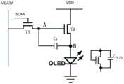
图1是2T1C结构的常规像素驱动电路。FIG. 1 is a conventional pixel driving circuit of a 2T1C structure.
图2是根据本公开的一些实施例的像素驱动电路的框图。FIG. 2 is a block diagram of a pixel driving circuit according to some embodiments of the present disclosure.
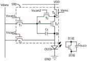
图3是根据本公开的实施例的包括5T1C结构的像素驱动电路。FIG. 3 is a pixel driving circuit including a 5T1C structure according to an embodiment of the present disclosure.
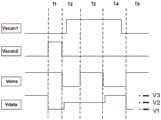
图4是根据本公开的实施例的操作全部为N型晶体管的图3的像素驱动电路的时序图。FIG. 4 is a timing diagram of the pixel driving circuit of FIG. 3 operating all N-type transistors according to an embodiment of the present disclosure.
图5是根据本公开的实施例的分别与在显示一个像素图像帧的一个周期的五个时间段中图3的像素驱动电路相对应的一系列有效电路示意图。FIG. 5 is a series of effective circuit schematic diagrams respectively corresponding to the pixel driving circuit of FIG. 3 in five time periods of one cycle of displaying one pixel image frame according to an embodiment of the present disclosure.
图6是根据本公开的另一实施例的包括5T1C结构的像素驱动电路。FIG. 6 is a pixel driving circuit including a 5T1C structure according to another embodiment of the present disclosure.
图7是根据本公开实施例的操作全部为N型晶体管的图6的像素驱动电路的时序图。FIG. 7 is a timing diagram of the pixel driving circuit of FIG. 6 in which all N-type transistors are operated according to an embodiment of the present disclosure.
图8是根据本公开的实施例的操作全部为P型晶体管的图3的像素驱动电路的时序图。FIG. 8 is a timing diagram of the pixel driving circuit of FIG. 3 operating all P-type transistors according to an embodiment of the present disclosure.
具体实施方式DETAILED DESCRIPTION
现在将参照以下实施例更具体地描述本公开。需注意,以下对一些实施例的描述仅针对示意和描述的目的而呈现于此。其不旨在是穷尽性的或者受限为所公开的确切形式。The present disclosure will now be described in more detail with reference to the following examples. It should be noted that the following description of some embodiments is presented here only for the purpose of illustration and description. It is not intended to be exhaustive or limited to the exact form disclosed.
有机发光二极管(OLED)被用作显示面板中每个子像素的LED元件。由正DC电流驱动的OLED器件可以在有机层中产生离子杂质的定向移动,从而引起内部电场,这减小了用于注入载流子的有效电场。有效地,这导致OLED的阈值电压增大。最终,更高的阈值电压劣化了OLED性能,使得器件的寿命缩短。常规像素驱动电路不具有补偿TFT和OLED两者的阈值电压从而实现显示面板令人满意的亮度均匀性的功能。Organic light emitting diodes (OLEDs) are used as LED elements for each sub-pixel in a display panel. OLED devices driven by positive DC current can produce directional movement of ionic impurities in the organic layer, thereby causing an internal electric field, which reduces the effective electric field for injecting carriers. Effectively, this leads to an increase in the threshold voltage of the OLED. Ultimately, a higher threshold voltage degrades the OLED performance, shortening the life of the device. Conventional pixel drive circuits do not have the function of compensating for the threshold voltages of both the TFT and the OLED to achieve satisfactory brightness uniformity of the display panel.
图1是与显示面板中的子像素相关联的具有2T1C结构的常规像素驱动电路。参照图1,当选择用于特定子像素的扫描线(SCAN)来施加导通电压时,第一晶体管T1导通。经由第一晶体管T1将电压信号VDATA写至存储电容器Cs的节点A(即,通过与另一节点B耦接的电容器Cs的电容有效地存储该电压)。由于第一晶体管T1工作在非饱和状态,第二晶体管T2构造为使其与节点A耦接的栅极以及与节点B耦接的源极具有等于VDATA的栅源电压Vgs。当未选择扫描线SCAN时,T1关断。电容器Cs所存储的电压能够导通第二晶体管T2。此外,第二晶体管T2产生(从其漏极至源极的)电流,以驱动OLED器件发光从而点亮子像素。第二晶体管T2构造为以饱和状态工作使得漏极电流由下式确定:FIG. 1 is a conventional pixel driving circuit with a 2T1C structure associated with a sub-pixel in a display panel. Referring to FIG. 1 , when a scan line (SCAN) for a particular sub-pixel is selected to apply a turn-on voltage, the first transistor T1 is turned on. The voltage signal VDATA is written to node A of the storage capacitor Cs via the first transistor T1 (i.e., the voltage is effectively stored by the capacitance of the capacitor Cs coupled to another node B). Since the first transistor T1 operates in a non-saturated state, the second transistor T2 is constructed so that its gate coupled to node A and the source coupled to node B have a gate-source voltage Vgs equal to VDATA. When the scan line SCAN is not selected, T1 is turned off. The voltage stored by the capacitor Cs can turn on the second transistor T2. In addition, the second transistor T2 generates a current (from its drain to the source) to drive the OLED device to emit light and thus light up the sub-pixel. The second transistor T2 is constructed to operate in a saturated state so that the drain current is determined by the following formula:

其中μn是TFT(即,T2)的电子载流子迁移率,COX是单位面积的绝缘电容,W/L是驱动晶体管T2的宽长比,Vgs是TFT T2的栅源电压,Vth是TFT T2的阈值电压。漏极电流是流过与作为TFT T2的源极的节点B直接耦接的OLED的电流。基于式(1),流过OLED的电流高度依赖于TFT的阈值电压Vth。Wherein μn is the electron carrier mobility of the TFT (i.e., T2), COX is the insulation capacitance per unit area, W/L is the width-to-length ratio of the driving transistor T2, Vgs is the gate-source voltage of the TFT T2, and Vth is the threshold voltage of the TFT T2. The drain current is the current flowing through the OLED directly coupled to the node B as the source of the TFT T2. Based on equation (1), the current flowing through the OLED is highly dependent on the threshold voltage Vth of the TFT.
因此,本公开特别提供了像素驱动电路、显示设备、以及驱动其像素驱动电路的方法,其实质上消除了由于现有技术的限制和缺陷而导致的问题中的一个或多个。在一方面,本公开提供了一种用于驱动与显示面板的子像素相关联的发光器件发光的像素驱动电路。图2是根据本公开的一些实施例的像素驱动电路的框图。Therefore, the present disclosure particularly provides a pixel driving circuit, a display device, and a method of driving the pixel driving circuit thereof, which substantially eliminates one or more of the problems caused by the limitations and defects of the prior art. In one aspect, the present disclosure provides a pixel driving circuit for driving a light-emitting device associated with a sub-pixel of a display panel to emit light. FIG2 is a block diagram of a pixel driving circuit according to some embodiments of the present disclosure.
参照图2,像素驱动电路100包括输入子电路10、调整子电路12、充电子电路14、驱动子电路16和存储子电路18。在一些实施例中,输入子电路10与数据线和第一节点A耦接,并且具有与第一扫描线耦接的控制端。输入子电路10构造为在供应至第一扫描线的第一控制信号的控制下将数据线中提供的任何电压电平写至第一节点A。调整子电路12分别与数据线、第二节点B和第三节点C耦接,并且具有与第二扫描线耦接的控制端以接收第二控制信号。调整子电路12构造为调整第一节点A处的电压电平并且将第一电压电平从数据线传递至第二节点B。如图所示,第二节点B旨在与发光器件LED耦接。可选地,LED是与显示面板中的子像素相关联的发光元件。特别地,第二节点B与LED的阳极耦接,所述LED示出为并联耦接的晶体管(具有共享的栅极和漏极)和有效电容器。LED的阴极构造为被提供有公共电压(例如,其连接至地)。替代性地,调整子电路12还构造为将电压电平从第三节点C传递至第一节点A以至少调整第一节点A的电压电平(其可以由输入子电路10预设)。2, the
在替代实施例中,调整子电路12分别与数据线、电源线和第二节点B耦接,并且具有与第二控制线耦接的控制端以接收第二控制信号。此外,调整子电路12还构造为将电源电压从电源线传递至第一节点A以至少调整第一节点A的电压电平(其可以由输入子电路10预设)。In an alternative embodiment, the
再次参照图2,充电子电路14经由第三节点C与驱动子电路16串联耦接。充电子电路14的一端与电源线耦接并且另一端(即,第三节点C)与驱动子电路16耦接。驱动子电路16还具有与第二节点B耦接的另一端。驱动子电路16构造为经由第二节点B向显示面板中的LED提供驱动电流以驱动发光。充电子电路14构造为对驱动子电路16充电以将第二节点B处的电压电平锁存为大于第一阈值电压但小于第二阈值电压。第一阈值电压和第二阈值电压两者是分别与驱动子电路16中的驱动晶体管和LED相关联的表征的物理性质。此外,参照图2,存储子电路18耦接在第一节点A与第二节点B之间以保持两者间的电压差。Referring again to FIG. 2 , the charging
在一些实施例中,像素驱动电路100构造为至少在显示像素图像帧的一个周期的多个时间段中的一个中由驱动子电路16产生流过LED的驱动电流。LED器件与显示面板中的子像素相关联。可选地,驱动电流与工作在饱和状态的驱动晶体管相关联。驱动电流实质上独立于驱动晶体管的第一阈值电压和LED器件的第二阈值电压。此外,像素驱动电路100还构造为将第二节点B(其还连接至LED的阳极)处的电压电平调整为低于LED的阴极的电压电平,使得至少在显示像素图像帧的该周期的多个时间段中的另一个中将LED设置为具有反向极性的状态。LED的反向极性有时有助于抑制LED中由于长时间偏压下离子杂质数量的增大而引起的电场。In some embodiments, the
图3是根据本公开的实施例的包括5T1C结构的像素驱动电路。这是像素驱动电路100的一个示例。参照图3,图2的输入子电路10包括第一晶体管T1,其栅极与第一扫描线连接,漏极与数据线Vdata连接,并且源极与第一节点A耦接。第一晶体管T1是开关晶体管,用于连接数据线Vdata以在供应至第一扫描线的第一控制信号Vscan1的控制下传递编程在Vdata中的电压,从而设置或改变第一节点A处的电压电平。FIG3 is a pixel driving circuit including a 5T1C structure according to an embodiment of the present disclosure. This is an example of a
在该示例中,图2的调整子电路12包括两个晶体管:第二晶体管T2和第三晶体管T3。第二晶体管T2具有与第二扫描线耦接的栅极、与电源线耦接的漏极、以及与第一节点A耦接的源极。第二晶体管T2是开关晶体管,用于连接第三节点C,以在供应至第二扫描线的第二控制信号Vscan2的控制下设置或调整第一节点A处的电压电平。第三晶体管T3具有也与第二扫描线耦接的栅极、与数据线Vdata耦接的漏极、以及与第二节点B耦接的源极。第三晶体管T3也是开关晶体管,用于连接数据线Vdata,以在来自第二扫描线的第二控制信号Vscan2的控制下设置或调整第二节点B处的电压电平。In this example, the
此外,在该示例中,图2的充电子电路14包括第四晶体管T4并且与图2的驱动子电路16连接,驱动子电路16包括作为驱动晶体管的第五晶体管T5。第四晶体管T4是开关晶体管,其栅极与控制线耦接,漏极与电源线耦接,并且源极连接至第三节点C并且还与第五晶体管T5的漏极串联连接。In addition, in this example, the charging
总之,这里的全部晶体管以薄膜晶体管或场效应晶体管构造,其具有控制端或栅极并且实质上源极和漏极对称地制成。这些晶体管中的每一个还构造为开关晶体管,其具有通过施加至控制端或栅极的导通电压的ON(导通)状态和通过施加至栅极的关断电压的OFF(关断)状态。对于N型晶体管,导通电压是高电压电平并且关断电压是低电压电平。In summary, all transistors here are constructed as thin film transistors or field effect transistors, which have a control terminal or gate and are substantially symmetrically made of source and drain. Each of these transistors is also constructed as a switching transistor, which has an ON state by a turn-on voltage applied to the control terminal or gate and an OFF state by a turn-off voltage applied to the gate. For N-type transistors, the turn-on voltage is a high voltage level and the turn-off voltage is a low voltage level.
参照图3,第五晶体管T5具有与第一节点A耦接的栅极、与第三节点C耦接的漏极、以及与第二节点B耦接的源极,第五晶体管T5构造为在饱和状态下受第一节点处的电压电平控制以产生驱动LED器件的驱动电流。处于ON状态的第四晶体管T4将电源线(被供有VDD)连接至第三节点C。如果第二晶体管T2也处于ON状态,则第一节点A可被写入来自电源线的电源电压VDD,从而导通第五晶体管T5。T5的ON状态允许电源电压VDD通过第五晶体管T5对第二节点B充电。可选地,像素驱动电路100中的全部晶体管可以替换为P型晶体管。可选地,电源电压VDD可以被供有不同电平,比如VDD1、VDD2或VDD3,这取决于操作周期中的不同时间段,特别对于操作具有P型的全部晶体管的像素驱动电路(将在下面示出)而言。Referring to Fig. 3, the fifth transistor T5 has a gate coupled to the first node A, a drain coupled to the third node C, and a source coupled to the second node B, and the fifth transistor T5 is configured to be controlled by the voltage level at the first node in a saturated state to generate a driving current for driving the LED device. The fourth transistor T4 in the ON state connects the power line (supplied with VDD) to the third node C. If the second transistor T2 is also in the ON state, the first node A can be written with the power supply voltage VDD from the power line, thereby turning on the fifth transistor T5. The ON state of T5 allows the power supply voltage VDD to charge the second node B through the fifth transistor T5. Optionally, all transistors in the
此外,在该示例中,图2的存储子电路18包括存储电容器Cs,其具有与第一节点A耦接的第一电极和与第二节点B耦接的第二电极。存储电容器Cs用于保持第一节点A与第二节点B之间的电压差,以至少锁存第五晶体管T5的第一阈值电压Vth的值。2 includes a storage capacitor Cs having a first electrode coupled to the first node A and a second electrode coupled to the second node B. The storage capacitor Cs is used to maintain a voltage difference between the first node A and the second node B to latch at least the value of the first threshold voltage Vth of the fifth transistor T5.
在实施例中,第一晶体管T1、第二晶体管T2、第三晶体管T3、第四晶体管T4、和第五晶体管(即,驱动晶体管)T5中的每一个是N型晶体管。可选地,LED器件为有机发光二极管(OLED)。可选地,像素驱动电路100形成在OLED显示面板中。在替代实施例中,通过适当调整晶体管和OLED在像素驱动电路中的位置,每个晶体管可以替换为P型晶体管。对于P型晶体管,导通电压是低电压电平并且关断电压是施加至相应栅极的高电压电平。In an embodiment, each of the first transistor T1, the second transistor T2, the third transistor T3, the fourth transistor T4, and the fifth transistor (i.e., the driving transistor) T5 is an N-type transistor. Optionally, the LED device is an organic light emitting diode (OLED). Optionally, the
参照图3,在该示例中,包含五个晶体管和一个电容器(5T1C)电路结构的像素驱动电路100与有机发光器件(OLED)耦接,发光器件(OLED)与显示面板中的一个子像素相关联。特别地,第二节点B与OLED的阳极耦接。OLED的阴极构造为被提供有公共电压(例如,阴极接地)。有效地,OLED示出为并联连接的晶体管(具有共享的栅极和漏极)和有效电容器COLED。操作像素驱动电路100以产生从驱动晶体管T5到其源极(也就是第二节点B)的驱动电流,从而在第二节点处或在OLED的阳极处给出相对于公共电压(例如,地)的特定电压电平Voled。由于当电压电平Voled大于OLED的第二阈值电压Vth_oled时驱动电流足够大,该驱动电流流过OLED并且驱动与子像素相关联的OLED发光以在每个周期产生像素图像。这里,一个周期指的是其中位于显示面板中的一行多个子像素的子像素刚好通过逐行扫描处理被扫描以在显示面板中显示图像帧的操作时间。Referring to FIG. 3 , in this example, a
为了操作像素驱动电路100以在显示像素图像帧的每个周期中产生驱动电流驱动OLED发光,像素驱动电路100还包括(连接至)供应有数据电压Vdata的数据线、供应有第一扫描信号Vscan1的第一扫描线、供应有第二扫描信号Vscan2的第二扫描线、供应有控制信号Vems的控制线、以及供应有正电压VDD的电源线。可选地,VDD可变化为不同值,比如VDD1<VDD2<VDD3。特别地,扫描或控制信号Vscan1、Vscan2、Vems中的每一个在每个周期的一个或多个时间段中被赋予低电压电平或高电压电平。可选地,低电压电平对应于能够关断N型开关晶体管或导通P型晶体管的控制信号。可选地,高电压电平对应于在像素驱动电路中导通N型薄膜晶体管(TFT)或关断P型TFT的控制信号。在实施例中,像素驱动电路100在每个周期的不同时间段中将第一控制信号Vscan1、第二控制信号Vscan2和第三控制信号Vems中的每一个编程为选择的低电压电平或高电压电平。此外,供应至数据线的数据电压Vdata被编程为比如其可以在每个周期的相应不同时间段中为负或为正。通过在选择的控制信号和编程的数据电压电平下操作像素驱动电路100,可以通过驱动电流驱动OLED在每个周期的一个时间段发光,所述驱动电流独立于驱动晶体管的第一阈值电压和OLED的第二阈值电压。此外,至少在每个周期的另一时间段中,特定类型的LED器件(有机发光二极管(OLED))可以设置为具有反向极性的状态,以防止空间电荷积聚在OLED的有机层内,从而增强其寿命。In order to operate the
在另一方面,本公开提供了一种驱动与显示面板的子像素相关联的发光元件以在显示一个像素图像帧的一个周期中发光的方法。在实施例中,驱动显示面板中的发光元件的方法包括:将发光元件的阳极处的电压电平设置为用于发光元件的反向极性的第一电压电平。所述方法还包括:将该电压电平调整为大于驱动晶体管的第一阈值电压的绝对值但是小于发光元件的第二阈值电压的一绝对值。第一阈值电压与像素驱动电路中使用的驱动晶体管相关联。可选地,像素驱动电路与图3中所示的与发光二极管串联耦接的像素驱动电路100相同。第二阈值电压与发光元件相关联。可选地,发光元件是有机发光二极管。此外,所述方法包括:将该电压电平改变至第二电压电平减第一阈值电压。此外,所述方法包括:基于处于第三电压电平的输入数据电压减耦合电压来更新该电压电平,所述耦合电压由固定电容器产生,所述固定电容器与有效电容器串联连接,所述有效电容器与所述发光元件相关联。此外,所述方法包括:产生独立于第一阈值电压和第二阈值电压的驱动电流以驱动发光元件发光。On the other hand, the present disclosure provides a method for driving a light-emitting element associated with a sub-pixel of a display panel to emit light in a cycle of displaying a pixel image frame. In an embodiment, the method for driving a light-emitting element in a display panel includes: setting a voltage level at an anode of the light-emitting element to a first voltage level of reverse polarity for the light-emitting element. The method also includes: adjusting the voltage level to an absolute value greater than the absolute value of the first threshold voltage of the driving transistor but less than the second threshold voltage of the light-emitting element. The first threshold voltage is associated with a driving transistor used in a pixel driving circuit. Optionally, the pixel driving circuit is the same as the
图4是根据本公开的实施例的操作全部为N型晶体管的图3的像素驱动电路100的时序图。如所述,一个周期时间被划分为五个顺序时间段,即,t1、t2、t3、t4和t5。因此,在每个时间段中提供对第一控制信号Vscan1、第二控制信号Vscan2、第三控制信号Vems和数据电压Vdata的设置或电压编程。图5是根据本公开的实施例的分别与在显示一个像素图像帧的一个周期的五个时间段t1、t2、t3、t4和t5中图3的像素驱动电路相对应的一系列有效电路示意图。结合图4中示出一个周期的五个时间段的时序图和图5中一个周期的五个时间段中的每一个中的有效电路,所述方法可以如下地示出。在该示例中,像素驱动电路100中的全部晶体管为N型晶体管。FIG. 4 is a timing diagram of the
参照图4,在每个周期开始,第一时间段是反向恢复时间段t1。在该时间段,第一控制信号Vscan1被设为与关断电压电平相对应的低电压电平。因此,第一晶体管T1关闭或关断。第三控制信号Vems被设为与导通电压电平相对应的高电压电平,从而导通第四晶体管T4。第二控制信号Vscan2被设为与导通电压电平相对应的高电压电平。因此,第二晶体管T2和第三晶体管T3导通。供应至数据线的数据电压Vdata被编程为第一电压电平V1。在该实施例中,V1给定为相对接地的负电压,即,V1<0。参照图5的第一部分,电源线被提供有正电源电压VDD。由于第二晶体管T2和第四晶体管T4导通,因此第一节点A通过T2和T4两者连接至电源线,从而使得第一极点A处的电压电平等于电源电压VDD,即,VA=VDD。由于第三晶体管T3导通,第一电压电平的Vdata被从数据线写至第二节点B,即,VB=V1<0。由于OLED的阳极连接至第二节点B并且OLED的阴极构造为被提供有公共电压(例如,其接地),使得OLED的阳极电压低于阴极电压。因此,在反向恢复时间段t1,OLED器件被设为具有反向极性的状态,其阴极电势电平高于阳极电势电平。使OLED进入反向极性状态的目的在于减小离子杂质电荷在有机层内的积累,使得器件的性能不会因为其常常在其应用期间处于正向极性下而随着时间快速劣化。Referring to FIG. 4 , at the beginning of each cycle, the first time period is a reverse recovery time period t1. During this time period, the first control signal Vscan1 is set to a low voltage level corresponding to the turn-off voltage level. Therefore, the first transistor T1 is turned off or turned off. The third control signal Vems is set to a high voltage level corresponding to the turn-on voltage level, thereby turning on the fourth transistor T4. The second control signal Vscan2 is set to a high voltage level corresponding to the turn-on voltage level. Therefore, the second transistor T2 and the third transistor T3 are turned on. The data voltage Vdata supplied to the data line is programmed to a first voltage level V1. In this embodiment, V1 is given as a negative voltage relative to ground, that is, V1<0. Referring to the first part of FIG. 5 , the power line is provided with a positive power supply voltage VDD. Since the second transistor T2 and the fourth transistor T4 are turned on, the first node A is connected to the power supply line through both T2 and T4, so that the voltage level at the first pole A is equal to the power supply voltage VDD, that is,VA =VDD. Since the third transistor T3 is turned on, Vdata of the first voltage level is written from the data line to the second node B, that is,VB = V1 < 0. Since the anode of the OLED is connected to the second node B and the cathode of the OLED is configured to be provided with a common voltage (for example, it is grounded), the anode voltage of the OLED is lower than the cathode voltage. Therefore, during the reverse recovery period t1, the OLED device is set to a state with a reverse polarity, and its cathode potential level is higher than the anode potential level. The purpose of putting the OLED into the reverse polarity state is to reduce the accumulation of ionic impurity charges in the organic layer so that the performance of the device does not deteriorate rapidly over time because it is often in a forward polarity during its application.
参照图4,顺序地在反向恢复时间段之后,该周期包括电压调整时间段t2。在该时间段,首先将第二控制信号Vscan2重置为关断(低)电压电平,以关断第二晶体管T2和第三晶体管T3。这使得存储电容器Cs的两个电极或两端处于悬置状态,从而保持其内存储的电荷不变。4, sequentially after the reverse recovery period, the cycle includes a voltage adjustment period t2. In this period, the second control signal Vscan2 is first reset to a turn-off (low) voltage level to turn off the second transistor T2 and the third transistor T3. This makes the two electrodes or both ends of the storage capacitor Cs suspended, thereby keeping the charge stored therein unchanged.
在重置第二控制信号Vscan2的稍后,供应至数据线的数据电压Vdata改变为第二电压电平V2,其被编程为高于第一电压电平V1但仍为负值,即,V1<V2<0。After a short while of resetting the second control signal Vscan2 , the data voltage Vdata supplied to the data line changes to a second voltage level V2 , which is programmed to be higher than the first voltage level V1 but still a negative value, ie, V1<V2<0.
在首先将第二控制信号Vscan2重置为关断(低)电压电平的稍后,第一控制信号Vscan1被重置为导通(高)电压电平,从而导通第一晶体管T1。因此,在该时间段,第一节点A被写有Vdata的电压电平,即,V2。换言之,第一节点A处的电压电平从VDD改变为V2,即,VA=V2。由于电容器Cs中的电荷守恒,因此随着第一节点A(电容器Cs的第一电极)处的电压电平的改变,第二节点B(电容器Cs的第二电极)处的电压电平也将基于电荷耦合效应而改变。After a while after first resetting the second control signal Vscan2 to the off (low) voltage level, the first control signal Vscan1 is reset to the on (high) voltage level, thereby turning on the first transistor T1. Therefore, during this period, the first node A is written with the voltage level of Vdata, that is, V2. In other words, the voltage level at the first node A changes from VDD to V2, that is, VA =V2. Due to the charge conservation in the capacitor Cs, as the voltage level at the first node A (the first electrode of the capacitor Cs) changes, the voltage level at the second node B (the second electrode of the capacitor Cs) will also change based on the charge coupling effect.
参照图5的第二部分,存储电容器Cs与OLED的有效电容器Coled经由第二节点B(即,OLED的阳极)串联地耦接,并且OLED的阴极构造为被提供有公共电压或其简单接地。因此,第二节点B处的电压电平将改变为
再次参照图4,顺序地在电压调整时间段之后,该周期包括阈值电压锁存时间段t3。在该时间段,第一控制信号Vscan1仍为高电压电平,以保持第一晶体管T1导通。第二控制信号Vscan2仍为关断(低)电压电平,以保持第二晶体管T2和第三晶体管T3关断。现在,第一节点A仍处于悬置状态,其电压电平为VA=V2。第三控制信号Vems被重置为导通(高)电压电平,从而导通第四晶体管T4。参照图5的第三部分,处于导通状态的第四晶体管T4将电源线与第五晶体管T5的漏极相连接,并且第五晶体管T5的栅极与第一节点A连接。因此,电源电压VDD被传递至第五晶体管T5的栅极和漏极,以对第五晶体管T5的源极进行充电,从而增大其电压电平。该充电效应持续,直到源极节点电压VB达到VA–Vth=V2–Vth。Referring again to FIG. 4 , sequentially after the voltage adjustment period, the cycle includes a threshold voltage latch period t3. During this period, the first control signal Vscan1 is still at a high voltage level to keep the first transistor T1 turned on. The second control signal Vscan2 is still at an off (low) voltage level to keep the second transistor T2 and the third transistor T3 turned off. Now, the first node A is still in a suspended state, and its voltage level isVA = V2. The third control signal Vems is reset to an on (high) voltage level, thereby turning on the fourth transistor T4. Referring to the third part of FIG. 5 , the fourth transistor T4 in the on state connects the power line to the drain of the fifth transistor T5, and the gate of the fifth transistor T5 is connected to the first node A. Therefore, the power supply voltage VDD is transferred to the gate and drain of the fifth transistor T5 to charge the source of the fifth transistor T5, thereby increasing its voltage level. This charging effect continues until the source node voltageVB reachesVA -Vth=V2-Vth.
上述第五晶体管T5的充电过程需要源极节点处的电压电平VB满足以下关系:


参照图4,顺序地在阈值电压锁存时间段之后,该周期包括数据电压输入时间段t4。在该时间段,第三控制信号Vems被重置为关断(低)电压电平,从而关断第四晶体管T4,以切断驱动晶体管T5的漏极与电源线的连接。第二控制信号Vscan2仍为关断(低)电压电平,以保持第二晶体管T2和第三晶体管T3关断。第一控制信号Vscan1仍为导通(高)电压电平,以保持第一晶体管T1导通,使得数据线中的任何电压改变将被写至第一节点A。Referring to Fig. 4, sequentially after the threshold voltage latching period, the cycle includes a data voltage input period t4. During this period, the third control signal Vems is reset to a turn-off (low) voltage level, thereby turning off the fourth transistor T4 to cut off the connection between the drain of the driving transistor T5 and the power line. The second control signal Vscan2 is still a turn-off (low) voltage level to keep the second transistor T2 and the third transistor T3 turned off. The first control signal Vscan1 is still a turn-on (high) voltage level to keep the first transistor T1 turned on, so that any voltage change in the data line will be written to the first node A.
在第三控制信号被重置为低电压电平的稍后,数据电压Vdata被供应数据线的第三电压电平V3,其被编程为正电压并且被写至第一节点A。参照图5的第四部分,数据电压V3是与实际图像数据相对应的电压,所述实际图像数据对应于与显示面板中的子像素相关联的OLED的发光的特定强度。现在,第一节点A处的电压电平从V2改变为V3,即,VA=V3。此时,由于与Coled串联连接的Cs的耦合效应,第二节点B处的电压电平VB也从V2-Vth改变为


再次参照图4,顺序地在数据电压输入时间段之后,该周期包括发光时间段t5。在该时间段,第二控制信号Vscan2保持为关断(低)电压电平,以保持第二晶体管T2和第三晶体管T3关断。第三控制信号Vems被重置为导通(高)电压电平,从而导通第四晶体管T4。在将第三控制信号Vems改变为高电压电平的稍早前,第一控制信号Vscan1被重置为关断(低)电压电平,从而关断第一晶体管T1以避免竞争。Referring again to FIG. 4 , sequentially after the data voltage input period, the cycle includes a light emitting period t5. During this period, the second control signal Vscan2 is maintained at an off (low) voltage level to keep the second transistor T2 and the third transistor T3 off. The third control signal Vems is reset to an on (high) voltage level, thereby turning on the fourth transistor T4. Slightly before the third control signal Vems is changed to a high voltage level, the first control signal Vscan1 is reset to an off (low) voltage level, thereby turning off the first transistor T1 to avoid competition.
参照图5的第五部分,与驱动晶体管T5的栅极连接的第一节点A保持为VA=V3。第二节点B连接至OLED的阳极,即,VB=Voled。存储电容器Cs将驱动晶体管T5的栅源电压继续保持为:

驱动晶体管产生的驱动电流Ioled可以表达为:The driving currentIoled generated by the driving transistor can be expressed as:

其中,
图6示出了根据本公开的另一实施例的包括5T1C结构的像素驱动电路。参照图6,像素驱动电路200包括:输入子电路,其与图2的输入子电路10实质上类似;调整子电路,其与图2的调整子电路12相比具有略微不同的连接;充电子电路,其与图2的充电子电路14实质上类似;驱动子电路和存储子电路,其与图2的驱动子电路16和存储子电路18实质上相同。在该实施例中,调整子电路也包括两个晶体管:第二晶体管T2和第三晶体管T3。第二晶体管T2具有与第二扫描线耦接的栅极、与电源线耦接的漏极、以及与第一节点A耦接的源极。第二晶体管T2是用于连接电源线的开关晶体管,从而在供应至第二扫描线的第二控制信号Vscan2的控制下传递电源电压VDD以设置或调整第一节点A处的电压电平。第三晶体管T3具有也与第二扫描线耦接的栅极、与数据线Vdata耦接的漏极、以及与第二节点B耦接的源极。第三晶体管T3也是开关晶体管,用于连接数据线Vdata以在来自第二扫描线的第二扫描信号Vscan2的控制下设置或调整第二节点B处的电压电平。除了像素驱动电路200的第二晶体管T2具有与图3的像素驱动电路100的第二晶体管T2的漏极的不同电路连接以外,其他晶体管T1、T3、T4和T5以及电容器Cs的所有其他电路连接与像素驱动电路100相同。FIG6 shows a pixel driving circuit including a 5T1C structure according to another embodiment of the present disclosure. Referring to FIG6 , the
图7是根据本公开的实施例的操作图6的像素驱动电路200的时序图。如所示的,一个周期时间被划分为五个顺序时间段,即,t1、t2、t3、t4和t5。相应地,在每个时间段中提供对第一控制信号Vscan1、第二控制信号Vscan2、第三控制信号Vems以及数据电压Vdata的设置或电压编程。FIG7 is a timing diagram of the
参照图7,在每个周期开始,第一时间段是反向恢复时间段t1。在该时间段,第一控制信号Vscan1被设为与晶体管关断电压相对应的低电压电平。因此,第一晶体管T1关闭或关断。第三控制信号Vems也被设为低电压电平以关断第四晶体管T4。第二控制信号Vscan2被设为与晶体管导通电压相对应的高电压电平。因此,第二晶体管T2和第三晶体管T3导通。供应至数据线的数据电压Vdata被编程为第一电压电平V1。在该实施例中,V1给定为相对于地的负电压,即,V1<0。参照图5的第一部分,电源线被提供有固定的正电源电压VDD。由于第二晶体管T2导通,因此第一节点A连接至电源线,从而使得第一极点A处的电压电平等于电源电压VDD,即,VA=VDD。由于第三晶体管T3导通,第一电压电平被写至第二节点B,即,VB=V1。由于OLED的阳极连接至第二节点B并且OLED的阴极接地,因此VB<0。因此,在反向恢复时间段t1,OLED器件被设为具有反向极性的状态,其阴极电势电平高于阳极电势电平。使OLED进入反向极性状态的目的在于减小离子杂质电荷在有机层内的积累,使得器件的性能不会因为其常常在其应用期间处于正向极性下而随着时间快速劣化。Referring to FIG. 7 , at the beginning of each cycle, the first time period is the reverse recovery time period t1. During this time period, the first control signal Vscan1 is set to a low voltage level corresponding to the transistor turn-off voltage. Therefore, the first transistor T1 is turned off or turned off. The third control signal Vems is also set to a low voltage level to turn off the fourth transistor T4. The second control signal Vscan2 is set to a high voltage level corresponding to the transistor turn-on voltage. Therefore, the second transistor T2 and the third transistor T3 are turned on. The data voltage Vdata supplied to the data line is programmed to the first voltage level V1. In this embodiment, V1 is given as a negative voltage relative to ground, that is, V1<0. Referring to the first part of FIG. 5 , the power line is provided with a fixed positive power supply voltage VDD. Since the second transistor T2 is turned on, the first node A is connected to the power supply line, so that the voltage level at the first pole A is equal to the power supply voltage VDD, that is,VA =VDD. Since the third transistor T3 is turned on, the first voltage level is written to the second node B, that is,VB =V1. Since the anode of the OLED is connected to the second node B and the cathode of the OLED is grounded,VB <0. Therefore, during the reverse recovery period t1, the OLED device is set to a state having a reverse polarity, with the cathode potential level being higher than the anode potential level. The purpose of bringing the OLED into the reverse polarity state is to reduce the accumulation of ionic impurity charges in the organic layer so that the performance of the device does not deteriorate rapidly over time because it is often in a forward polarity during its application.
参照图4和图7,从第二时间段(电压调整时间段t2)开始,图7中关于所有控制信号Vscan1、Vscan2、Vems和数据信号Vdata的时序波形与图4中的时序波形实质上相同。因此,图6的像素驱动电路200的操作与图3的像素驱动电路100的操作实质上相同。4 and 7, starting from the second time period (voltage adjustment time period t2), the timing waveforms of all control signals Vscan1, Vscan2, Vems and data signal Vdata in FIG7 are substantially the same as the timing waveforms in FIG4. Therefore, the operation of the
在另一替代实施例中,图3的像素驱动电路100可以提供为全部是P型晶体管。图8是根据本公开的实施例的操作全部为P型晶体管的图3的像素驱动电路的时序图。参照图8,在第一时间段t1(即,反向恢复时间段),第一控制信号Vscan1被提供有关断(高)电压电平,以关断第一晶体管T1。第三控制信号Vems被提供有导通(低)电压电平,从而导通第四晶体管T4。第二控制信号Vscan2被设为导通(低)电压电平,以导通第二晶体管T2和第三晶体管T3两者。来自电源线的电源电压给定为VDD2,其经由T4和T2传递至第一节点A,即,VA=VDD2。数据电压Vdata=V2经由T3被写至第二节点B,即,VB=V2。V2给定为负电压(V2<0)。可选地,VDD2被设为小于V2以使得第五晶体管T5关断。OLED的阳极电压为VB。OLED的阴极电压为接地。VB<0,所以,OLED在反向恢复时间段中被设为反向极性状态。这有助于清除在OLED的操作期间积累的残余电荷,从而恢复其物理特性并延长寿命。In another alternative embodiment, the
参照图8,在下一时间段t2(即,电压调整时间段),第二控制信号Vscan2被设为关断(高)电压电平,以关断T2和T3。第三控制信号Vems也被设为关断电压电平以关断T4,使得电容器Cs的两端(即,第一节点A和第二节点B)处于悬置状态,从而保存其中存储的电荷。随后,在设置第三控制信号Vems为关断电压电平的稍后,第一控制信号Vscan1被设为导通(低)电压电平以导通T1,从而将第一节点A的电压电平改变为VA=V3>V2。根据电容器Cs以及与OLED相关联的有效电容器Coled的耦合效应,第二节点B的电压电平变为VB=V2–(VDD2–V3)Cs/(Cs+Coled)。8 , in the next time period t2 (i.e., the voltage adjustment time period), the second control signal Vscan2 is set to the off (high) voltage level to turn off T2 and T3. The third control signal Vems is also set to the off voltage level to turn off T4, so that both ends of the capacitor Cs (i.e., the first node A and the second node B) are in a suspended state, thereby preserving the charges stored therein. Subsequently, shortly after setting the third control signal Vems to the off voltage level, the first control signal Vscan1 is set to the on (low) voltage level to turn on T1, thereby changing the voltage level of the first node A toVA = V3> V2. According to the coupling effect of the capacitor Cs and the effective capacitor Coled associated with the OLED, the voltage level of the second node B becomesVB = V2–(VDD2–V3)Cs/(Cs+Coled).
参照图8,在下一时间段t3(即,阈值电压锁存时间段),第一控制信号Vscan1仍为导通(低)电压电平,使得T1保持导通。第三控制信号Vems改变为导通(低)电压电平,以导通T4。第一节点A仍为电压电平V3。在该时间段,电源电压跳至VDD1<VDD2。可选地,VDD1的值设为VDD1<V3<VB=V2–(VDD2–V3)Cs/(Cs+Coled)。OLED的阳极电压VB将通过T4和T5被电源电压充电。充电效应持续,直到第五晶体管T5的源极(即,第二节点B)的电压电平达到值V3+Vth,这里,Vth是与第五晶体管T5(P型)相关联的第一阈值电压。因此,该第一阈值电压被锁存至电容器Cs中。注意,充电和锁存过程只有在以下条件满足时才有效:
参照图8,在下一时间段t4(即,数据输入时间段),第一控制信号Vscan1仍为导通(低)电压电平,使得T1保持导通。第三控制信号Vems被设为关断(高)电压电平,从而关断T4。电源电压VDD跳至VDD3>VDD2。数据电压(现在处于不同的电压电平V1)被输入至第一节点A,即,VA=V1。随后,耦合效应使得第二节点B的电压电平被改变为VB=(V3+Vth)+(V1–V3)Cs/(Cs+Coled)。存储在电容器Cs中的电压将保存为:8 , in the next time period t4 (i.e., data input time period), the first control signal Vscan1 is still at the on (low) voltage level, so that T1 remains on. The third control signal Vems is set to the off (high) voltage level, thereby turning off T4. The power supply voltage VDD jumps to VDD3>VDD2. The data voltage (now at a different voltage level V1) is input to the first node A, i.e.,VA = V1. Subsequently, the coupling effect causes the voltage level of the second node B to be changed toVB = (V3+Vth) + (V1–V3)Cs/(Cs+Coled). The voltage stored in the capacitor Cs will be saved as:
V1–VB=[(V3+Vth)+(V1–V3)Cs/(Cs+Coled)]=-Vth+(V1–V3)Coled/(Cs+Coled)V1–VB =[(V3+Vth)+(V1–V3)Cs/(Cs+Coled)]=-Vth+(V1–V3)Coled/(Cs+Coled)
为了避免在每个周期(除了设计的发光时间段)中不必要的发光,阳极(或第二节点B)的电压电平应当保持在VB<Vth_oled,这里,Vth_oled是OLED开始发光时的阳极电压,其也被定义为本公开稍早部分中描述的第二阈值电压。To avoid unnecessary light emission in each cycle (except the designed light emission period), the voltage level of the anode (or the second node B) should be maintained atVB < Vth_oled, where Vth_oled is the anode voltage when the OLED starts to emit light, which is also defined as the second threshold voltage described earlier in this disclosure.
再次参照图8,在下一时间段t5(即,发光时间段),第二控制信号Vscan2保持为关断(高)电压电平以保持T2和T3关断,而第一控制信号Vscan1被改变为关断(高)电压电平以关断T1。第三控制信号Vems改变为导通(低)电压电平,从而导通T4。这里,早于将第三控制信号Vems设为导通电压电平地执行将第一控制信号Vscan1设置为关断电压电平,从而避免竞争。在该时间段,通过来自第五晶体管T5的驱动电流驱动OLED以发光。T5工作在饱和状态,这是因为第二节点B的电压电平VB=Voled。电容器Cs持续保持栅源电压Vgs为:Referring again to FIG. 8 , in the next time period t5 (i.e., the light-emitting time period), the second control signal Vscan2 is maintained at the off (high) voltage level to keep T2 and T3 off, while the first control signal Vscan1 is changed to the off (high) voltage level to turn off T1. The third control signal Vems is changed to the on (low) voltage level, thereby turning on T4. Here, setting the first control signal Vscan1 to the off voltage level is performed earlier than setting the third control signal Vems to the on voltage level, thereby avoiding competition. In this time period, the OLED is driven to emit light by the driving current from the fifth transistor T5. T5 operates in a saturated state because the voltage level VB of the second nodeB = Voled. The capacitor Cs continues to maintain the gate-source voltage Vgs as:
Vgs=-Vth+(V1–V3)Coled/(Cs+Coled)Vgs=-Vth+(V1–V3)Coled/(Cs+Coled)
驱动晶体管T5(P型)产生的驱动电流Ioled可以表达为:The driving current Ioled generated by the driving transistor T5 (P type) can be expressed as:

从式(3)可以看出,发光时间段流过OLED的驱动电流独立于驱动晶体管T5的第一阈值电压Vth和OLED的第二阈值电压Vth_oled。驱动电流仅受到输入的数据电压Vdata的影响,所述数据电压Vdata在每个周期的不同时间段中以不同电平来编程。It can be seen from equation (3) that the driving current flowing through the OLED during the light-emitting period is independent of the first threshold voltage Vth of the driving transistor T5 and the second threshold voltage Vth_oled of the OLED. The driving current is only affected by the input data voltage Vdata, which is programmed with different levels in different time periods of each cycle.
在又一替代实施例中,图6的像素驱动电路200可以提供为全部是P型晶体管。相应地,操作全部为P型晶体管的图6的像素驱动电路200的时序图可以通过如下方式提供:仅修改图8的第一时间段t1以使得第三控制信号Vems被提供有关断(高)电压电平以关断第四晶体管T4,同时其他控制信号设置为与图8的那些相同。来自电源线的电源电压给定为VDD2,其经由T2传递至第一节点A,即,VA=VDD2。数据电压Vdata=V2经由T3被写至第二节点B,即,VB=V2。V2给定为负电压(V2<0)。可选地,VDD2被设为小于V2以使得第五晶体管T5关断。OLED的阳极电压为VB。OLED的阴极电压为接地。VB<0,所以,OLED在反向恢复时间段中被设为反向极性状态。这有助于清除在OLED的操作期间积累的残余电荷,从而恢复其物理特性并延长寿命。对于该示例中的所有其它阶段t2、t3、t4和图5,所有控制信号提供为与图8的那些相同。因此,全部为P型晶体管的像素驱动电路200在这些时间段中的相应操作将与先前所示的那些相同。In yet another alternative embodiment, the
在另一方面,本公开提供了一种显示设备,其包括显示面板和本文所述的像素驱动电路。在一个示例中,显示设备中的像素驱动电路实质上与图2所示的像素驱动电路100相同,或者与图3的特定实施例相同,其包括五个晶体管和一个电容器作为基本结构,该基本结构与数据线、第一扫描线、第二扫描线、控制线和电源线耦接。所述五个晶体管中的每一个是N型晶体管。可选地,所述五个晶体管中的每一个是P型晶体管。在另一示例中,该显示设备中的像素驱动电路与图6中所示的像素驱动电路200实质上相同,包括作为基本结构的五个晶体管和一个电容器,该基本结构与数据线、第一扫描线、第二扫描线、控制线和电源线耦接。可选地,所述五个晶体管中的每一个是N型晶体管。可选地,所述五个晶体管中的每一个是P型晶体管。像素驱动电路是与显示面板中的多个子像素中的一个相关联的发光器件的阳极耦接的多个单元电路中的一个。可选地,发光器件是有机发光二极管,其具有构造为被提供有公共电压(例如,被接地)的阴极。可选地,显示面板为有机发光二极管显示面板。适当显示设备的示例包括但不限于:电子纸、移动电话、平板计算机、电视、监视器、笔记本计算机、数字相框、GPS等。在一个示例中,显示设备为智能手表。可选地,所述显示设备为有机发光二极管显示设备。On the other hand, the present disclosure provides a display device, which includes a display panel and a pixel driving circuit described herein. In one example, the pixel driving circuit in the display device is substantially the same as the
出于示意和描述目的已示出对本发明实施例的上述描述。其并非旨在穷举或将本发明限制为所公开的确切形式或示例性实施例。因此,上述描述应当被认为是示意性的而非限制性的。显然,许多修改和变形对于本领域技术人员而言将是显而易见的。选择和描述这些实施例是为了解释本发明的原理和其最佳方式的实际应用,从而使得本领域技术人员能够理解本发明适用于特定用途或所构思的实施方式的各种实施例及各种变型。本发明的范围旨在由所附权利要求及其等同形式限定,其中除非另有说明,否则所有术语以其最宽的合理意义解释。因此,术语“发明”、“本发明”等不一定将权利范围限制为具体实施例,并且对本发明示例性实施例的参考不隐含对本发明的限制,并且不应推断出这种限制。本发明仅由随附权利要求的精神和范围限定。此外,这些权利要求可涉及使用跟随有名词或元素的“第一”、“第二”等术语。这种术语应当理解为一种命名方式而非意在对由这种命名方式修饰的元素的数量进行限制,除非给出具体数量。所描述的任何优点和益处不一定适用于本发明的全部实施例。应当认识到的是,本领域技术人员在不脱离随附权利要求所限定的本发明的范围的情况下可以对所描述的实施例进行变化。此外,本公开中没有元件和组件是意在贡献给公众的,无论该元件或组件是否明确地记载在随附权利要求中。The above description of the embodiments of the present invention has been shown for the purpose of illustration and description. It is not intended to be exhaustive or to limit the present invention to the exact form or exemplary embodiment disclosed. Therefore, the above description should be considered as illustrative rather than restrictive. Obviously, many modifications and variations will be obvious to those skilled in the art. These embodiments are selected and described to explain the principles of the present invention and the practical application of the best mode thereof, so that those skilled in the art can understand the various embodiments and various variations of the present invention applicable to specific uses or conceived embodiments. The scope of the present invention is intended to be limited by the appended claims and their equivalents, wherein all terms are interpreted in their broadest reasonable sense unless otherwise stated. Therefore, the terms "invention", "present invention" and the like do not necessarily limit the scope of rights to specific embodiments, and reference to exemplary embodiments of the present invention does not imply a limitation of the present invention, and such limitation should not be inferred. The present invention is limited only by the spirit and scope of the appended claims. In addition, these claims may involve the use of terms such as "first", "second" and the like followed by nouns or elements. Such terms should be understood as a naming method rather than intended to limit the number of elements modified by such naming methods unless a specific number is given. Any advantages and benefits described are not necessarily applicable to all embodiments of the present invention. It should be appreciated that those skilled in the art may make changes to the described embodiments without departing from the scope of the invention as defined by the appended claims. In addition, no element or assembly is intended to be dedicated to the public in this disclosure, regardless of whether the element or assembly is explicitly recorded in the appended claims.
Claims (13)
Applications Claiming Priority (1)
| Application Number | Priority Date | Filing Date | Title |
|---|---|---|---|
| PCT/CN2018/096802WO2020019158A1 (en) | 2018-07-24 | 2018-07-24 | Pixel driving circuit, method, and display apparatus |
Publications (2)
| Publication Number | Publication Date |
|---|---|
| CN109074777A CN109074777A (en) | 2018-12-21 |
| CN109074777Btrue CN109074777B (en) | 2023-04-28 |
Family
ID=64789419
Family Applications (1)
| Application Number | Title | Priority Date | Filing Date |
|---|---|---|---|
| CN201880000867.3AActiveCN109074777B (en) | 2018-07-24 | 2018-07-24 | Pixel driving circuit, method, and display device |
Country Status (3)
| Country | Link |
|---|---|
| US (1) | US11289022B2 (en) |
| CN (1) | CN109074777B (en) |
| WO (1) | WO2020019158A1 (en) |
Families Citing this family (4)
| Publication number | Priority date | Publication date | Assignee | Title |
|---|---|---|---|---|
| CN110010071B (en) | 2019-04-18 | 2021-03-23 | 京东方科技集团股份有限公司 | Pixel compensation circuit, driving method thereof, display panel and display device |
| CN115335892A (en)* | 2020-03-27 | 2022-11-11 | 索尼半导体解决方案公司 | Driving circuit, display device and driving method |
| KR20240117705A (en)* | 2023-01-26 | 2024-08-02 | 엘지디스플레이 주식회사 | Pixel circuit and display device including the same |
| CN117953813B (en)* | 2024-03-26 | 2024-06-21 | 深圳市华星光电半导体显示技术有限公司 | Display panel, display control method thereof and display device |
Family Cites Families (18)
| Publication number | Priority date | Publication date | Assignee | Title |
|---|---|---|---|---|
| JP4327042B2 (en)* | 2004-08-05 | 2009-09-09 | シャープ株式会社 | Display device and driving method thereof |
| US7663615B2 (en)* | 2004-12-13 | 2010-02-16 | Casio Computer Co., Ltd. | Light emission drive circuit and its drive control method and display unit and its display drive method |
| JP4923410B2 (en)* | 2005-02-02 | 2012-04-25 | ソニー株式会社 | Pixel circuit and display device |
| KR100719924B1 (en)* | 2005-04-29 | 2007-05-18 | 비오이 하이디스 테크놀로지 주식회사 | Organic electroluminescent display |
| JP2007108378A (en)* | 2005-10-13 | 2007-04-26 | Sony Corp | Driving method of display device and display device |
| US8004477B2 (en)* | 2005-11-14 | 2011-08-23 | Sony Corporation | Display apparatus and driving method thereof |
| KR101214205B1 (en)* | 2005-12-02 | 2012-12-21 | 재단법인서울대학교산학협력재단 | Display device and driving method thereof |
| JP4168290B2 (en)* | 2006-08-03 | 2008-10-22 | ソニー株式会社 | Display device |
| JP4222426B2 (en)* | 2006-09-26 | 2009-02-12 | カシオ計算機株式会社 | Display driving device and driving method thereof, and display device and driving method thereof |
| JP2008233501A (en)* | 2007-03-20 | 2008-10-02 | Sony Corp | Driving method of organic electroluminescence light emitting unit |
| CN102044212B (en)* | 2009-10-21 | 2013-03-20 | 京东方科技集团股份有限公司 | Voltage driving pixel circuit, driving method thereof and organic lighting emitting display (OLED) |
| JP5146521B2 (en)* | 2009-12-28 | 2013-02-20 | カシオ計算機株式会社 | Pixel drive device, light emitting device, drive control method thereof, and electronic apparatus |
| CN101996579A (en)* | 2010-10-26 | 2011-03-30 | 华南理工大学 | Pixel driving circuit and method of active organic electroluminescent display |
| US10453398B2 (en)* | 2013-06-20 | 2019-10-22 | Sharp Kabushiki Kaisha | Display apparatus and driving method thereof |
| KR102389343B1 (en)* | 2015-08-27 | 2022-04-25 | 삼성디스플레이 주식회사 | Pixel, organic light emitting display device including the pixel and driving method of the pixel |
| JP2017134145A (en)* | 2016-01-26 | 2017-08-03 | 株式会社ジャパンディスプレイ | Display device |
| CN105528992A (en)* | 2016-01-29 | 2016-04-27 | 深圳市华星光电技术有限公司 | Pixel compensating circuit, method, scanning drive circuit and plane display device |
| KR102547401B1 (en)* | 2016-07-12 | 2023-06-26 | 삼성디스플레이 주식회사 | Emitting light display device |
- 2018
- 2018-07-24CNCN201880000867.3Apatent/CN109074777B/enactiveActive
- 2018-07-24WOPCT/CN2018/096802patent/WO2020019158A1/ennot_activeCeased
- 2018-07-24USUS16/476,688patent/US11289022B2/enactiveActive
Also Published As
| Publication number | Publication date |
|---|---|
| US20210358413A1 (en) | 2021-11-18 |
| US11289022B2 (en) | 2022-03-29 |
| CN109074777A (en) | 2018-12-21 |
| WO2020019158A1 (en) | 2020-01-30 |
Similar Documents
| Publication | Publication Date | Title |
|---|---|---|
| JP5063433B2 (en) | Display device | |
| JP6882591B2 (en) | AMOLED pixel drive circuit and pixel drive method | |
| CN103165080B (en) | Pixel circuit and driving method and display device thereof | |
| CN111613180A (en) | AMOLED pixel compensation driving circuit and method and display panel | |
| CN100578593C (en) | Pixel circuit of active organic light emitting device | |
| CN110164375B (en) | Pixel compensation circuit, driving method, electroluminescence display panel and display device | |
| CN101986378A (en) | Pixel driving circuit for active organic light-emitting diode (OLED) display and driving method thereof | |
| CN111599313B (en) | Pixel driving circuit, driving method and display panel | |
| CN108777131B (en) | AMOLED pixel driving circuit and driving method | |
| JP2004361640A (en) | Pixel circuit, display device, and driving method for pixel circuit | |
| WO2005045797A1 (en) | Pixel circuit, display apparatus, and method for driving pixel circuit | |
| CN104318899B (en) | Pixel unit driving circuit and method, pixel unit and display device | |
| CN104318894A (en) | Pixel circuit and driving method thereof, and display apparatus | |
| CN109074777B (en) | Pixel driving circuit, method, and display device | |
| CN103198794A (en) | Pixel circuit, drive method, organic luminance display panel and display device thereof | |
| JP2009169239A (en) | Self-luminous display device and driving method thereof | |
| CN104616621B (en) | Pixel circuit, and drive method and display device thereof | |
| WO2021000816A1 (en) | Pixel circuit and driving method therefor, and display device | |
| JP5073544B2 (en) | Display device | |
| WO2016119305A1 (en) | Amoled pixel drive circuit and pixel drive method | |
| CN108538243A (en) | Display device, pixel-driving circuit and its driving method | |
| JP2008051990A (en) | Display device | |
| CN111292684A (en) | Display panel, pixel driving circuit and control method thereof | |
| JP6788755B2 (en) | AMOLED pixel drive circuit and pixel drive method | |
| CN113870785B (en) | OLED pixel compensation circuit and OLED pixel compensation method |
Legal Events
| Date | Code | Title | Description |
|---|---|---|---|
| PB01 | Publication | ||
| PB01 | Publication | ||
| SE01 | Entry into force of request for substantive examination | ||
| SE01 | Entry into force of request for substantive examination | ||
| GR01 | Patent grant | ||
| GR01 | Patent grant |