CN109071325B - Sealing unit with transparent laser welded area - Google Patents
Sealing unit with transparent laser welded areaDownload PDFInfo
- Publication number
- CN109071325B CN109071325BCN201780016429.1ACN201780016429ACN109071325BCN 109071325 BCN109071325 BCN 109071325BCN 201780016429 ACN201780016429 ACN 201780016429ACN 109071325 BCN109071325 BCN 109071325B
- Authority
- CN
- China
- Prior art keywords
- substrate
- glass
- laser
- inorganic film
- stress
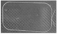
- Prior art date
- Legal status (The legal status is an assumption and is not a legal conclusion. Google has not performed a legal analysis and makes no representation as to the accuracy of the status listed.)
- Active
Links
Images


Landscapes
- Joining Of Glass To Other Materials (AREA)
Abstract
Description
Translated fromChinese相关申请的交叉引用CROSS-REFERENCE TO RELATED APPLICATIONS
本申请要求以下专利申请的优先权权益:2016年3月10日提交的题为“SealedDevices Comprising Transparent Laser Weld Regions”[《包含透明激光焊接区域的密封装置》]的第15/066704号美国专利申请;2014年5月7日提交的题为“Laser WeldingTransparent Glass Sheets Using Low Melting Glass Or Thin Absorbing Films”[《使用低熔点玻璃或薄吸收膜对透明玻璃片进行激光焊接》]的第14/271,797号美国专利申请,该美国专利申请要求以下美国临时申请的优先权权益:2013年5月10日提交的题为“LaserWelding Transparent Glass Sheet Using Low Melting Glass Film”[《使用低熔点玻璃膜对透明玻璃片进行激光焊接》]的第61/822,048号美国临时申请;2013年10月4日提交的题为“Laser Welding Transparent Glass Sheets Using Ultraviolet Absorbing Film”[《使用紫外吸收膜对透明玻璃片进行激光焊接》]的第61/886,928号美国临时申请;和2013年5月31日提交的题为“Laser Sealing Using Low Melting Temperature Glass forHermetic Devices”[《使用低熔化温度玻璃对气密性装置进行激光密封》]的第61/829,379号美国临时申请,本文以上述每件申请的内容为基础,并将其通过引用的方式全文纳入本文。This application claims the benefit of priority to the following patent application: US Patent Application No. 15/066704, filed March 10, 2016, entitled "SealedDevices Comprising Transparent Laser Weld Regions" ; No. 14/271,797, "Laser Welding Transparent Glass Sheets Using Low Melting Glass Or Thin Absorbing Films", filed May 7, 2014 U.S. Patent Application, which claims the priority benefit of the following U.S. Provisional Application: "LaserWelding Transparent Glass Sheet Using Low Melting Glass Film", filed May 10, 2013 U.S. Provisional Application No. 61/822,048; "Laser Welding Transparent Glass Sheets Using Ultraviolet Absorbing Film", filed Oct. 4, 2013 ["Laser Welding Transparent Glass Sheets Using Ultraviolet Absorbing Film"] ] of U.S. Provisional Application No. 61/886,928; and "Laser Sealing Using Low Melting Temperature Glass for Hermetic Devices", filed May 31, 2013 US Provisional Application No. 61/829,379 of , which is hereby incorporated by reference in its entirety, is based on the contents of each of the aforementioned applications.
技术领域technical field
本公开一般涉及密封装置以及包含所述密封装置的电子部件和显示部件,更具体而言,涉及包含透明焊接区域的密封玻璃装置。The present disclosure generally relates to sealing devices and electronic and display components including the same, and more particularly, to sealing glass devices that include transparent solder regions.
背景技术Background technique
许多现代装置要求密封环境来进行操作,并且其中许多是需要电偏置的“有源”装置。显示器,例如需要透光性和光偏置的有机发光二极管(OLED),由于使用电子注入材料需要绝对气密性,因此是高要求的应用。除此以外,这些材料一般会在几秒内在大气中分解,因此相应的装置应长时间保持真空或惰性气氛。另外,由于待包封的有机材料的温度敏感性高,因此气密性密封应在近环境温度下进行。Many modern devices require a sealed environment to operate, and many of these are "active" devices that require electrical biasing. Displays, such as Organic Light Emitting Diodes (OLEDs) which require light transmission and light biasing, are demanding applications due to the use of electron injection materials requiring absolute hermeticity. In addition to this, these materials generally decompose in the atmosphere within seconds, so corresponding devices should be kept in vacuum or inert atmosphere for long periods of time. Additionally, due to the high temperature sensitivity of the organic material to be encapsulated, hermetic sealing should be performed at near ambient temperature.
基于玻璃料的密封剂包括例如研磨到粒径通常在约2至150微米范围内的玻璃材料。对于玻璃料密封应用来说,通常将玻璃料材料与粒径相近的负CTE材料混合,并且使用有机溶剂或粘合剂将得到的混合物掺混到糊料中。示例性的负CTE无机填料包括堇青石颗粒(例如Mg2Al3[AlSi5O18])、硅酸钡、β-锂霞石、钒酸锆(ZrV2O7)或钨酸锆(ZrW2O8),将它们添加到玻璃料中来形成糊料以降低基材与玻璃料之间的热膨胀系数错配。溶剂用于调整合并的粉末和有机粘合剂糊料的流变粘度,并且这些溶剂需适于受控的分配目的。为了使两个基材结合,可以通过旋涂或丝网印刷将玻璃料层施涂到一个或两个基材的密封表面上。经过玻璃料涂覆的基材初始在相对较低的温度下经受有机烧尽步骤(例如,在250℃下进行30分钟),以去除有机载体。然后,沿着相应的密封表面,对待结合的两个基材进行组装/匹配,并将该对基材放入晶片结合器中。在明确限定的温度和压力下执行热压缩循环,由此熔化玻璃料以形成紧凑的玻璃密封件。除去某些含铅组合物外,玻璃料材料的玻璃化转变温度通常大于450℃,因此需要在高温下加工以形成阻挡层。这样的高温密封工艺对温度敏感型工件来说可能是不利的。另外,为了减小通常的基材与玻璃料之间的热膨胀系数错配,使用负CTE无机填料,这些负CTE无机填料将被包含到结合接头中,并导致基于玻璃料的阻挡层基本上不透明。基于上述,期望在低温下形成透明且气密的玻璃-玻璃密封件、玻璃-金属密封件、玻璃-陶瓷密封件及其他密封件。Glass frit-based encapsulants include, for example, glass materials ground to particle sizes typically in the range of about 2 to 150 microns. For frit sealing applications, the frit material is typically mixed with a negative CTE material of similar particle size, and the resulting mixture is blended into a paste using an organic solvent or binder. Exemplary negative CTE inorganic fillers include cordierite particles (eg, Mg2 Al3 [AlSi5 O18 ]), barium silicate, beta-eucryptite, zirconium vanadate (ZrV2 O7 ), or zirconium tungstate (ZrW2 O8 ), which are added to the glass frit to form a paste to reduce the thermal expansion coefficient mismatch between the substrate and the glass frit. Solvents are used to adjust the rheological viscosity of the combined powder and organic binder paste, and these solvents need to be suitable for controlled dispensing purposes. To bond the two substrates, a frit layer can be applied to the sealing surfaces of one or both substrates by spin coating or screen printing. The frit-coated substrate is initially subjected to an organic burnout step at a relatively low temperature (eg, at 250°C for 30 minutes) to remove the organic vehicle. Then, along the respective sealing surfaces, the two substrates to be bonded are assembled/matched, and the pair of substrates is placed in the wafer bonder. A thermal compression cycle is performed at well-defined temperatures and pressures, thereby melting the frit to form a compact glass seal. With the exception of certain lead-containing compositions, glass frit materials typically have glass transition temperatures greater than 450°C and therefore require processing at elevated temperatures to form the barrier layer. Such a high temperature sealing process can be disadvantageous for temperature sensitive workpieces. Additionally, in order to reduce the thermal expansion coefficient mismatch between the usual substrate and glass frit, negative CTE inorganic fillers are used, which will be incorporated into the bond joint and result in a substantially opaque glass frit based barrier layer . Based on the above, it is desirable to form transparent and hermetic glass-glass seals, glass-metal seals, glass-ceramic seals, and other seals at low temperatures.
虽然常规的玻璃基材激光焊接可使用超大功率激光装置,但是这种在近激光烧蚀下的操作常常损坏玻璃基材并得到质量较差的气密性密封件。再者,这种常规方法使得到的装置的不透明度增加,并且还提供了低质量的密封件。While conventional laser welding of glass substrates can use ultra-high power laser devices, this operation under near-laser ablation often damages the glass substrate and results in poor quality hermetic seals. Again, this conventional approach results in increased opacity of the resulting device and also provides a low quality seal.
在一些情况中,密封件可能不是光学透明的,例如可能是着色的。在用于对光进行发射、透射、转换、提取、漫射和/或散射的密封封装件的情形中,这些缺陷尤为不利。例如,不透明的密封件可以阻挡光透射,而光学不透明的密封件可能在光通过密封区域时使光发生不期望的畸变。由于这些原因,通常围绕基材外周施涂密封剂,例如施涂在围绕待密封物体的框架中,或者仅在边缘处施涂,即使封装件中未密封物体。尽管如此,在一些构造中,边缘处的材料仍可使光发生不期望的畸变或使光透射减小。In some cases, the seal may not be optically clear, eg, may be colored. These defects are particularly disadvantageous in the context of hermetic packages used to emit, transmit, convert, extract, diffuse and/or scatter light. For example, opaque seals can block light transmission, while optically opaque seals can undesirably distort light as it passes through the sealed area. For these reasons, sealants are typically applied around the periphery of the substrate, for example in a frame around the object to be sealed, or only at the edges, even if the object is not sealed in the package. Nonetheless, in some configurations, the material at the edges can undesirably distort the light or reduce light transmission.
因此,有利的是,提供对基材进行激光密封的方法,该方法除了其他优点之外,还可以增加密封件的透明度、强度和/或气密性,降低制造成本和/或复杂性,并且/或者提高生产率和/或产率。还会有利的是,提供用于显示器和其他电子装置的密封装置,其可使光透射性得到改进和/或使畸变减少。得到的密封装置自身可用作显示器或其他电子装置中的部件,或者可用于保护各种电子器件和其他部件,例如发光结构或颜色转换元件,例如激光二极管(LD)、LED、OLED和/或QD。Accordingly, it would be advantageous to provide a method of laser sealing a substrate that, among other advantages, increases the transparency, strength and/or air tightness of the seal, reduces manufacturing cost and/or complexity, and /or increase productivity and/or productivity. It would also be advantageous to provide sealing arrangements for displays and other electronic devices that would result in improved light transmission and/or reduced distortion. The resulting encapsulated device can itself be used as a component in displays or other electronic devices, or can be used to protect various electronic devices and other components, such as light emitting structures or color conversion elements such as laser diodes (LDs), LEDs, OLEDs and/or QD.
发明内容SUMMARY OF THE INVENTION
本公开的实施方式一般涉及气密性阻挡层,更具体地,涉及使用吸收薄膜来密封固体结构的方法和组合物。本公开的实施方式提供了使用薄膜作为界面引发剂,对玻璃片和其他材料片进行激光焊接或密封的方法,所述薄膜在密封过程中具有吸收特性。根据一些实施方式,示例性的激光焊接条件可适于在导电性界面膜上进行焊接,并且导电性的下降可忽略不计。因此,所述实施方式可用于形成有源装置(例如OLED或其他装置)的气密性封装件,并且能够广泛、大批量地制造合适的玻璃或半导体封装件。应注意的是,术语密封、结合、接合和焊接在本公开中可互换使用并且是互换使用的。这种用法不应当限制本文所附的权利要求书的范围。还应注意的是,在本公开中,当术语玻璃和无机涉及对名词膜进行修饰时,它们可互换使用,并且这种用法不应当限制本文所附的权利要求书的范围。Embodiments of the present disclosure relate generally to hermetic barriers and, more particularly, to methods and compositions for sealing solid structures using absorbent films. Embodiments of the present disclosure provide methods for laser welding or sealing sheets of glass and other materials using thin films as interfacial initiators, the films having absorbing properties during the sealing process. According to some embodiments, exemplary laser welding conditions may be suitable for welding on conductive interface films with negligible drop in conductivity. Thus, the described embodiments can be used to form hermetic packages for active devices, such as OLEDs or other devices, and enable the wide-scale, high-volume manufacture of suitable glass or semiconductor packages. It should be noted that the terms sealing, bonding, joining and welding are used interchangeably and interchangeably in this disclosure. Such usage should not limit the scope of the claims appended hereto. It should also be noted that in this disclosure, when the terms glass and inorganic refer to modifications to the noun membrane, they are used interchangeably, and such usage should not limit the scope of the claims appended hereto.
本公开的实施方式提供了一种激光密封方法,例如激光焊接、漫射焊接等,所述方法可在两个玻璃之间的界面处提供吸收膜。在稳定状态中,吸收可以大于或高达约70%,或者可以小于或低至约10%。小于或低至10%的吸收依赖于在入射激光波长下,在玻璃基材中的色心形成并结合示例性的激光吸收膜,而该色心形成是由于外在色心(例如杂质或掺杂剂)或玻璃固有的内在色心所致。膜的一些非限制性实例包括Tg<600℃的SnO2、ZnO、TiO2、ITO、UV吸收玻璃膜,以及低熔点玻璃(LMG)或低液相线温度(LLT)膜(无玻璃化转变温度的材料),它们可用于玻璃基材的界面处。例如,LLT材料可以包括但不限于陶瓷、玻璃陶瓷和玻璃材料。例如,LLT玻璃可包括锡氟磷酸盐玻璃、掺钨的锡氟磷酸盐玻璃、硫属化合物玻璃、亚碲酸盐玻璃、硼酸盐玻璃和磷酸盐玻璃。在另一个非限制性实施方式中,密封材料可以为含Sn2+的无机氧化物材料,例如,SnO、SnO+P2O5和SnO+BPO4。其他非限制性实例可以包括吸收峰在>800nm波长处的近红外(NIR)吸收玻璃膜。使用这些材料的焊接可提供可见光透射,并且具有足够的UV或NIR吸收来引发温和的稳态扩散焊接。这些材料还可提供具有局部密封温度,并且该温度适于进行扩散焊接的透明激光焊接件。这种扩散焊接使相应的玻璃基材进行低功率和低温激光焊接,并且可以以有效且快速的焊接速度产生优异的透明焊接件。根据本公开的实施方式所述的示例性激光焊接工艺还可依赖于色心形成后的玻璃的光诱导吸收特性,以包括温度诱导吸收。Embodiments of the present disclosure provide a laser sealing method, such as laser welding, diffusion welding, etc., that can provide an absorbing film at the interface between two glasses. In a steady state, the absorption may be greater than or as high as about 70%, or may be less than or as low as about 10%. Absorption of less than or as low as 10% depends on the formation of color centers in the glass substrate at the incident laser wavelength due to extrinsic color centers (e.g. impurities or doping) in combination with exemplary laser absorbing films. impurities) or the inherent color center of glass. Some non-limiting examples of films include SnO2, ZnO, TiO2, ITO, UV absorbing glass films with Tg < 600°C, and low melting glass (LMG) or low liquidus temperature (LLT) films (no glass transition temperature). material), they can be used at the interface of glass substrates. For example, LLT materials may include, but are not limited to, ceramics, glass ceramics, and glass materials. For example, LLT glasses may include tin fluorophosphate glasses, tungsten-doped tin fluorophosphate glasses, chalcogenide glasses, tellurite glasses, borate glasses, and phosphate glasses. In another non-limiting embodiment, the sealing material may be a Sn2+ containing inorganic oxide material, eg, SnO, SnO+P2 O5 and SnO+BPO4 . Other non-limiting examples may include near-infrared (NIR) absorbing glass films with absorption peaks at >800 nm wavelengths. Welding with these materials provides visible light transmission with sufficient UV or NIR absorption to induce mild steady-state diffusion welding. These materials can also provide transparent laser welds with local sealing temperatures suitable for diffusion welding. This diffusion welding enables low-power and low-temperature laser welding of the corresponding glass substrates and can produce excellent transparent welds at efficient and fast welding speeds. Exemplary laser welding processes according to embodiments of the present disclosure may also rely on the light-induced absorption properties of the glass after color center formation to include temperature-induced absorption.
本文描述了使用低熔点无机(LMG)材料或紫外吸收(UVA)或红外吸收(IRA)材料的界面薄膜,利用激光将各透明玻璃片焊接在一起以引发密封的现象。在示例性实施方式中,描述了实现强结合形成的三个标准:(1)示例性的LMG或UVA或IRA膜可在透明度窗口(例如约420nm至约750nm)以外的入射波长下充分吸收,以将足够的热传播到玻璃基材中,并且玻璃基材可因此表现出(2)温度诱导的吸收和(3)在入射波长下形成瞬态色心。测量表明形成了热压缩扩散焊接机制,其定性地导致形成极强的结合。本文还描述了与焊接工艺相关的温度事件的演变以及激光焊接中色心形成过程的明显普遍性。还论述了LMG或UVA材料与Eagle
本公开的另外的实施方式提供了具有低温结合形成和“直接玻璃密封”的激光密封方法,其中,可在入射波长下将透明玻璃密封到吸光玻璃(absorbing glass),从而形成在可见波长400-700nm下的不透明密封件。在示例性实施方式中,两块玻璃在入射激光波长下以及在可见波长范围中均是透明的或几乎是透明的。得到的密封件在可见波长范围中也是透明的,其对照明应用来说是吸引人的,因为在密封位置处不吸收光,因此不会产生与密封相关的热堆积。另外,由于可将膜施加在整个盖板玻璃上方,因此无需精确分配密封用玻璃糊料来进行密封操作,从而为装置制造商提供了很大的自由度来改变他们的密封图案而不需要对密封区域进行特殊的图案化或加工。在其他实施方式中,还可在玻璃区域的某些点上进行密封以形成用于机械稳定性的非气密性结合。此外,可在弯曲的共型表面上进行所述密封。Additional embodiments of the present disclosure provide laser sealing methods with low temperature bond formation and "direct glass sealing", wherein transparent glass can be sealed to absorbing glass at incident wavelengths, thereby forming 400- Opaque seal at 700nm. In an exemplary embodiment, both glasses are transparent or nearly transparent at the incident laser wavelength and in the visible wavelength range. The resulting seal is also transparent in the visible wavelength range, which is attractive for lighting applications because no light is absorbed at the location of the seal and thus no seal-related heat build-up occurs. Additionally, since the film can be applied over the entire cover glass, there is no need to precisely dispense the sealing glass paste for the sealing operation, giving device manufacturers a great deal of freedom to change their sealing pattern without the need for The sealing area is specially patterned or machined. In other embodiments, sealing may also be performed at certain points in the glass area to form a non-hermetic bond for mechanical stability. Furthermore, the sealing can be performed on curved conformal surfaces.
本公开的实施方式提供了低熔化温度材料,其可以用于将玻璃片激光焊接在一起,这涉及焊接任意的玻璃而不考虑玻璃的CTE差异。另外的实施方式可提供玻璃基材的对称焊接(即,厚玻璃与厚玻璃的焊接),例如Eagle与Eagle的焊接、Lotus与Lotus的焊接等。一些实施方式可使用导热板来提供玻璃基材的不对称焊接(即,薄玻璃与厚玻璃的焊接),例如Willow与Eagle
实施方式还提供了用于将玻璃封装件激光焊接在一起的材料,从而能够对对氧和湿气侵袭所导致的降解敏感的无源和有源装置进行长久气密操作。示例性的LMG或其他吸收薄膜密封件在将各结合表面组装后可以利用激光吸收被热活化,并且可以具有更高的制造效率,因为密封每个工作装置的速率由热活化和结合形成决定,而不是由通过在真空或惰性气体组装线中的在线(inline)薄膜沉积对装置进行封装的速率决定。在UV或NIR-IR密封件中的示例性的LMG、LLT及其他吸收薄膜还能够对大片多重装置进行密封,随后刻划或切成各个装置(单个化),并且由于机械完整性高,因此单个化的产率可以较高。Embodiments also provide materials for laser welding glass packages together, enabling long-term hermetic operation of passive and active devices that are sensitive to degradation due to oxygen and moisture aggression. Exemplary LMG or other absorptive film seals can be thermally activated using laser absorption after the individual bonding surfaces are assembled, and can have higher manufacturing efficiencies because the rate at which each working device is sealed is determined by thermal activation and bond formation, Rather, it is determined by the rate at which the device is packaged by inline thin film deposition in a vacuum or inert gas assembly line. Exemplary LMG, LLT, and other absorbing films in UV or NIR-IR seals also enable sealing of large sheets of multiple devices, subsequent scoring or dicing of individual devices (singulated), and due to high mechanical integrity, The yield of singulation can be higher.
在一些实施方式中,结合工件的方法包括在第一基材表面的上方形成无机膜;将待受保护的工件布置在第一基材与第二基材之间,其中,使所述膜与第二基材接触;以及通过利用具有预定波长的激光辐射对膜进行局部加热而将工件结合在第一基材与第二基材之间。无机膜、第一基材或第二基材在约420nm至约750nm下可具有透射性。In some embodiments, the method of bonding workpieces includes forming an inorganic film over a surface of a first substrate; disposing the workpiece to be protected between the first substrate and the second substrate, wherein the film is caused to contacting the second substrate; and bonding the workpiece between the first substrate and the second substrate by locally heating the film with laser radiation having a predetermined wavelength. The inorganic film, the first substrate, or the second substrate may have transmittance at about 420 nm to about 750 nm.
在其他实施方式中,提供了一种结合装置,其包括在第一基材表面上方形成的无机膜,以及在第一基材与第二基材之间的受保护的装置,其中,无机膜与第二基材接触。在这样的实施方式中,所述装置包括通过用具有预定波长的激光辐射来局部加热无机膜而在第一基材与第二基材之间形成的结合,其根据第一或第二基材中的杂质组成变化而变化,并且根据无机膜的组成变化而变化。另外,无机膜、第一基材或第二基材在约420nm至约750nm下可具有透射性。In other embodiments, a bonding device is provided that includes an inorganic film formed over a surface of a first substrate, and a protected device between the first substrate and the second substrate, wherein the inorganic film in contact with the second substrate. In such embodiments, the device includes a bond formed between the first substrate and the second substrate by locally heating the inorganic film with laser radiation having a predetermined wavelength, depending on whether the first or second substrate The impurity composition in the film changes, and it changes according to the composition change of the inorganic film. In addition, the inorganic film, the first substrate, or the second substrate may have transmittance at about 420 nm to about 750 nm.
在另外的实施方式中,提供了一种对装置进行保护的方法,所述方法包括在第一基材的第一部分表面上方形成无机膜层;将待受保护的装置布置在第一基材与第二基材之间,其中使密封层与第二基材接触;以及使用激光辐射局部加热无机膜层和第一及第二基材以使密封层和基材熔化而在各基材之间形成密封。第一基材可包括玻璃或玻璃陶瓷,而第二基材可包括玻璃、金属、玻璃陶瓷或陶瓷。In further embodiments, a method of protecting a device is provided, the method comprising forming an inorganic film layer over a first portion of a surface of a first substrate; disposing the device to be protected on the first substrate and the between the second substrates, wherein the sealing layer is brought into contact with the second substrate; and the inorganic film layer and the first and second substrates are locally heated using laser radiation to melt the sealing layer and the substrates between the substrates form a seal. The first substrate may comprise glass or glass-ceramic, and the second substrate may comprise glass, metal, glass-ceramic or ceramic.
在各个实施方式中,本公开还涉及密封装置,其包括在第一基材表面上方形成的无机膜;与无机膜接触的第二基材;和焊接区域,所述焊接区域包括在第一基材和第二基材之间形成的结合,并且该焊接区域从第一基材中的第一深度延伸到第二基材中的第二深度。根据另外的实施方式,无机膜包括至少一种无机膜元素,并且第一基材和第二基材中的一种或两种包括至少一种无机基材元素。在另外的实施方式中,在焊接区域中的第一或第二基材的第一无机膜元素浓度高于焊接区域外的第一或第二基材的第二无机膜元素浓度。根据另外的实施方式,在焊接区域中的第一基材元素浓度高于焊接区域外的无机膜的第二基材元素浓度。在另外的实施方式中,可以在第二基材表面上方形成第二无机膜。In various embodiments, the present disclosure also relates to a sealing device that includes an inorganic film formed over a surface of a first substrate; a second substrate in contact with the inorganic film; and a welding region, the welding region comprising a surface of the first substrate A bond is formed between the material and the second substrate, and the welded region extends from a first depth in the first substrate to a second depth in the second substrate. According to further embodiments, the inorganic film includes at least one inorganic film element, and one or both of the first substrate and the second substrate include at least one inorganic substrate element. In further embodiments, the concentration of the first inorganic film element of the first or second substrate in the weld zone is higher than the concentration of the second inorganic film element of the first or second substrate outside the weld zone. According to further embodiments, the concentration of the first substrate element in the weld zone is higher than the second substrate element concentration of the inorganic film outside the weld zone. In further embodiments, a second inorganic film may be formed over the surface of the second substrate.
在一些实施方式中,无机膜和任选地第一或第二基材中的至少一种在约420nm至约750nm范围内的波长下具有透射性。在另外的实施方式中,第一基材、第二基材和无机膜中的每一种在约420nm至约750nm范围内的波长下均可以具有透射性。在其他实施方式中,焊接区域可以是透明的。第一基材或第二基材中的一者或二者可以选自玻璃或玻璃陶瓷,例如钠钙硅酸盐玻璃、硅铝酸盐玻璃、碱金属硅铝酸盐玻璃、硼硅酸盐玻璃、碱金属硼硅酸盐玻璃、铝硼硅酸盐玻璃、碱金属铝硼硅酸盐玻璃和碱土金属铝硼硅酸盐玻璃。根据某些实施方式,第一基材或第二基材可以包括聚合物、陶瓷或金属。In some embodiments, at least one of the inorganic film and optionally the first or second substrate is transmissive at wavelengths in the range of about 420 nm to about 750 nm. In further embodiments, each of the first substrate, the second substrate, and the inorganic film may be transmissive at wavelengths in the range of about 420 nm to about 750 nm. In other embodiments, the weld area may be transparent. One or both of the first substrate or the second substrate may be selected from glass or glass ceramics, such as soda lime silicate glass, aluminosilicate glass, alkali metal aluminosilicate glass, borosilicate glass Glass, alkali metal borosilicate glass, aluminoborosilicate glass, alkali metal aluminoborosilicate glass and alkaline earth metal aluminoborosilicate glass. According to certain embodiments, the first substrate or the second substrate may comprise polymers, ceramics or metals.
无机膜可以具有包含以下物质的组合物:20-100摩尔%SnO;0-50摩尔%SnF2;和0-30摩尔%P2O5或B2O3。无机膜还可以具有包含以下物质的组合物:10-80摩尔%B2O3;5-60摩尔%Bi2O3;和0-70摩尔%ZnO。根据各个实施方式,无机膜的厚度可在约0.1微米至约10微米的范围内。在另外的实施方式中,焊接区域的厚度可以在约0.3微米至约14微米的范围内。The inorganic film may have a composition comprising: 20-100 mol %SnO ; 0-50 mol %SnF2; and 0-30 mol %P2O5 orB2O3 .The inorganic film may also have a composition comprising: 10-80 mol% B2O3; 5-60 mol%Bi2O3; and 0-70 mol% ZnO. According to various embodiments, the thickness of the inorganic film may range from about 0.1 microns to about 10 microns. In further embodiments, the thickness of the weld region may be in the range of about 0.3 microns to about 14 microns.
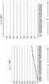
在一些实施方式中,密封装置还可包括至少包围焊接区域的应力区域,其中,应力区域中的第一应力大于应力区域外的第二应力。例如,第一应力可在大于约1MPa至约25MPa的范围内。在另外的实施方式中,第一应力相对于第二应力的比值在约1.1:1至约25:1的范围内。根据某些实施方式,应力区域的厚度可在约20微米至约500微米的范围内。In some embodiments, the sealing device may further include a stress region surrounding at least the weld region, wherein the first stress in the stress region is greater than the second stress outside the stress region. For example, the first stress may be in the range of greater than about 1 MPa to about 25 MPa. In further embodiments, the ratio of the first stress to the second stress is in the range of about 1.1:1 to about 25:1. According to certain embodiments, the thickness of the stressed region may range from about 20 microns to about 500 microns.
本文还公开了密封装置,其包括在第一基材表面上方形成的无机膜;与无机膜接触的第二基材;以及焊接区域,所述焊接区域包括在第一基材与第二基材之间形成的结合。根据另外的实施方式,第一基材和第二基材中的一种或两种包括至少一种无机基材元素。在另外的实施方式中,焊接区域相比于焊接区域外的一部分无机膜富含所述至少一种无机基材元素。本文还公开了密封装置,其包括在第一基材表面上方形成的无机膜;与无机膜接触的第二基材;以及焊接区域,所述焊接区域包括在第一基材与第二基材之间形成的结合。根据另外的实施方式,无机膜包括至少一种无机膜元素。在另外的实施方式中,第一或第二基材包括在焊接区域中的第一部分和在焊接区域外的第二部分。根据另外的实施方式,相比于第二部分,第一部分富含所述至少一种无机膜元素。在另外的实施方式中,可以在第二基材表面上方形成第二无机膜。Also disclosed herein is a sealing device comprising an inorganic film formed over the surface of the first substrate; a second substrate in contact with the inorganic film; and a welding region comprising the first substrate and the second substrate combination formed between. According to further embodiments, one or both of the first substrate and the second substrate comprise at least one inorganic substrate element. In further embodiments, the weld area is enriched with the at least one inorganic substrate element compared to a portion of the inorganic film outside the weld area. Also disclosed herein is a sealing device comprising an inorganic film formed over the surface of the first substrate; a second substrate in contact with the inorganic film; and a welding region comprising the first substrate and the second substrate combination formed between. According to further embodiments, the inorganic film includes at least one inorganic film element. In further embodiments, the first or second substrate includes a first portion in the weld zone and a second portion outside the weld zone. According to a further embodiment, the first part is enriched in the at least one inorganic membrane element compared to the second part. In further embodiments, a second inorganic film may be formed over the surface of the second substrate.
在以下的详细描述中提出了要求保护的主题的另外的特征和优点,其中的部分特征和优点对本领域的技术人员而言根据所作描述即容易理解,或者通过实施包括以下具体实施方式、权利要求书以及附图在内的本文所述的要求保护的主题而被认识。Additional features and advantages of the claimed subject matter are set forth in the following detailed description, some of which are readily apparent to those skilled in the art from the description, or by practice including the following detailed description, claims The claimed subject matter described herein, including the book and drawings, is recognized.
应当理解的是,前面的一般性描述和以下的具体实施方式都描述了本公开的实施方式且都旨在提供用于理解所要求保护的主题的性质和特性的总体评述或框架。所包含的附图供进一步理解本公开,附图被结合在本说明书中并构成说明书的一部分。附图例示了各个实施方式,且与说明书一起用于解释所要求保护的主题的原理和操作。It is to be understood that both the foregoing general description and the following detailed description describe embodiments of the present disclosure and are both intended to provide a general overview or framework for understanding the nature and character of the claimed subject matter. The accompanying drawings are included to provide a further understanding of the present disclosure, and are incorporated in and constitute a part of this specification. The drawings illustrate various embodiments, and together with the description serve to explain the principles and operation of the claimed subject matter.
附图说明Description of drawings
出于说明的目的提供了这些附图,应当理解的是,本文公开和论述的实施方式不限于所示的布置和机构。These figures are provided for illustrative purposes, it being understood that the embodiments disclosed and discussed herein are not limited to the arrangements and instrumentalities shown.
图1是根据本公开的一个实施方式所述的激光焊接的一个示例性过程图。FIG. 1 is an exemplary process diagram of laser welding according to an embodiment of the present disclosure.
图2是例示了通过一个实施方式的激光密封形成气密性密封装置的示意图。FIG. 2 is a schematic diagram illustrating the formation of a hermetic sealing device by laser sealing of one embodiment.
图3为本主题的另一个实施方式的图。Figure 3 is a diagram of another embodiment of the subject matter.
图4是用于估计激光焊接结合区的物理范围的实验布置示意图。Figure 4 is a schematic diagram of the experimental setup used to estimate the physical extent of the laser welded bond area.
图5是断裂样品的显微图像。Figure 5 is a microscopic image of a fractured sample.
图6是根据本公开的一些实施方式所述的建模方案示意图。6 is a schematic diagram of a modeling scheme according to some embodiments of the present disclosure.
图7是根据本公开的实施方式所述的另一个建模方案。FIG. 7 is another modeling scheme according to an embodiment of the present disclosure.
图8是通过Eagle 0.7mm玻璃基材的355nm激光透射率(%T)用于%T相对于时间测量的实验布置图。8 is a graph of the experimental setup for %T versus time measurement of 355 nm laser transmittance (%T) through Eagle 0.7 mm glass substrates.
图9是根据本公开的一个实施方式所述的图。FIG. 9 is a diagram according to one embodiment of the present disclosure.
图10是分析了在玻璃界面处,从LMG膜层进入到Eagle
图11是在不同厚度的玻璃片之间的激光焊接性能的示意图。Figure 11 is a graphical representation of laser welding performance between glass sheets of different thicknesses.
图12是估算在ITO引线(leads)上方的激光焊接范围的实验示意图。Figure 12 is a schematic diagram of an experiment to estimate the extent of laser welding over ITO leads.
图13提供了在ITO图案化膜上方形成的激光密封线的照片。Figure 13 provides a photograph of a laser seal line formed over an ITO patterned film.
图14是在图案化膜上方形成的另外的激光密封线的照片。Figure 14 is a photograph of an additional laser seal line formed over the patterned film.
图15是根据一些实施方式所述的另一种方法的简化图。15 is a simplified diagram of another method according to some embodiments.
图16是一些实施方式的两层激光加热表面吸收模型。16 is a two-layer laser-heated surface absorption model of some embodiments.
图17是一些实施方式的一系列温度变化图。Figure 17 is a series of temperature change graphs for some embodiments.
图18是针对一些实施方式的,在扫掠激光的停留时间内沉积的一系列平均能量图。Figure 18 is a series of plots of average energy deposited over the dwell time of the swept laser for some embodiments.
图19是在用IR辐射源加热期间,在355nm下的Eagle

图20是一些实施方式在加热期间在355nm下的玻璃透射性图。Figure 20 is a graph of glass transmittance at 355 nm during heating for some embodiments.
图21是一些实施方式在UV辐射期间和之后,对膜和基材的透射性的影响图。Figure 21 is a graph of the effect of some embodiments on the transmittance of films and substrates during and after UV radiation.
图22是一些实施方式的吸收相对于波长的图。Figure 22 is a graph of absorption versus wavelength for some embodiments.
图23是在Eagle
图24是在Eagle
图25是一些实施方式在激光焊接时观察到的界面接触几何范围示意图。25 is a schematic illustration of the geometric range of interfacial contact observed during laser welding for some embodiments.
图26是在施加的恒定压力P外下,在对界面间隙区域进行激光焊接期间,相对接触区域Ac/A0的演变示意图。Figure 26 is a schematic diagram of the evolution of the relative contact areaAc /A0 during laser welding of the interfacial gap area underan applied constant pressure P.
图27例示了使用通常的激光焊接条件在一个实施方式的激光扫掠区域上方的轮廓仪迹线。Figure 27 illustrates a profiler trace over the laser swept region of one embodiment using typical laser welding conditions.
图28是提供了针对一些实施方式估算的焊接速率比较情况的一系列图。28 is a series of graphs that provide a comparison of estimated weld rates for some embodiments.
图29是一些实施方式的偏振测量和图像的示意图。Figure 29 is a schematic diagram of polarization measurements and images of some embodiments.
图30是根据示例性焊接线提供应力位置的图。30 is a diagram of providing stress locations according to an exemplary weld line.
图31是根据一些实施方式所述的经过激光焊接的钠钙玻璃的一系列照片。31 is a series of photographs of laser welded soda lime glass according to some embodiments.
图32是一些实施方式的示意图。Figure 32 is a schematic diagram of some embodiments.
图33-34是一些实施方式中的焊接线的照片。33-34 are photographs of weld lines in some embodiments.
图35A是包含两个基材和无机膜的制品的侧视图。Figure 35A is a side view of an article comprising two substrates and an inorganic film.
图35B是经受一种示例性密封工艺的一种制品的顶视图。35B is a top view of an article undergoing an exemplary sealing process.
图35C是根据本公开的各个实施方式所述的密封装置的截面图。35C is a cross-sectional view of a sealing device according to various embodiments of the present disclosure.
图36A-36B是分别是在激光密封之前和之后的密封界面的SEM图像。36A-36B are SEM images of the sealed interface before and after laser sealing, respectively.
图37例示了用于元素分析的经过焊接的制品和示例性区域。Figure 37 illustrates welded articles and exemplary regions for elemental analysis.
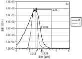
图38A-38C例示了在密封制品的焊接区域和非焊接区域中的元素深度分布(F、P、Sn)的各个图。38A-38C illustrate various graphs of elemental depth distribution (F, P, Sn) in welded and non-welded areas of a sealed article.
图39A-39C例示了在密封制品的焊接区域和非焊接区域中的元素深度分布(Al、B、Si)的各个图。39A-39C illustrate various graphs of elemental depth distribution (Al, B, Si) in welded and non-welded regions of a sealed article.
图40例示了根据本公开的各个实施方式,密封装置的应力分布随着深度变化而变化的各个图。40 illustrates various graphs of stress distribution of a sealing arrangement as a function of depth, according to various embodiments of the present disclosure.
虽然本说明书可包括许多特定情况,但这些不构成本公开的范围的限制,而是描述对于具体的实施方式特定的特征。Although this specification may contain many specific situations, these should not be construed as limitations on the scope of the disclosure but rather as descriptions of features specific to particular implementations.
具体实施方式Detailed ways
参考附图描述了密封方法和密封装置的各个实施方式,其中为了便于理解,相同元件以相同的附图标记给出。Various embodiments of the sealing method and sealing device are described with reference to the accompanying drawings, wherein like elements are given like reference numerals for ease of understanding.
还应理解,除非另外说明,否则,术语例如“顶部”、“底部”、“向外”、“向内”等是为了方便起见的用语,不应视为限制性用语。此外,每当将一个组描述为包含一组元素和它们的组合中的至少一种时,所述组可以单个元素或相互组合的形式包含任何数量的这些所列元素,或者主要由任何数量的这些所列元素组成,或者由任何数量的这些所列元素组成。It should also be understood that unless stated otherwise, terms such as "top," "bottom," "outward," "inward," etc. are terms of convenience and should not be regarded as limiting. Furthermore, whenever a group is described as containing at least one of a group of elements and combinations thereof, the group can contain any number of those listed elements, either individually or in combination with one another, or consist essentially of any number of elements consists of, or consists of, any number of, these listed elements.
类似地,每当将一个组描述为由一组元素中的至少一个元素或它们的组合组成时,所述组可以单个元素或相互组合的形式由任何数量的这些所列元素组成。除非另有说明,否则,所列举的数值范围同时包括所述范围的上限和下限。除非另外说明,否则,本文所用的不定冠词“一个”和“一种”及其相应的定冠词“该/所述”表示“至少一(个/种)”,或者“一(个/种)或多(个/种)”。Similarly, whenever a group is described as consisting of at least one of the group of elements, or a combination thereof, the group can consist of any number of the listed elements, either individually or in combination with one another. Unless otherwise indicated, recited numerical ranges include both the upper and lower limits of the stated range. Unless stated otherwise, the indefinite articles "a" and "an" and their corresponding definite articles "the/the" as used herein mean "at least one", or "an" species) or multiple (one/species)”.
本领域的技术人员能够认识到,可以对所述实施方式做出许多改变,同时仍能获得本发明的有益效果。还应显而易见的是,本公开的期望益处中的一部分可以通过选择一些所述特征而不利用其他特征来获得。因此,本领域技术人员应认识到,许多更改和修改都是可能的,在某些情况下甚至是希望的,并且是本公开的一部分。因此,提供以下描述作为对本公开原理的说明而不构成对本公开的限制。Those skilled in the art will recognize that many changes can be made to the described embodiments while still obtaining the benefits of the present invention. It should also be apparent that some of the desired benefits of the present disclosure may be obtained by selecting some of the described features without utilizing other features. Accordingly, those skilled in the art will recognize that many changes and modifications are possible, and in some cases even desirable, and are a part of this disclosure. Accordingly, the following description is provided as an illustration of the principles of the present disclosure and is not intended to limit the disclosure.
本领域技术人员应理解,在不偏离本发明的精神和范围的情况下,可对本文所述的示例性实施方式进行许多修改。因此,本发明的描述并非意在受限于所给出的实例,也不应理解为受限于所给出的实例,而应被赋予由所附权利要求书及其等同体提供的全部保护范围。此外,可以利用本公开的一些特性而不相应地利用其他特性。因此,前面提供对示例性或说明性实施方式的描述的目的在于说明本公开的原理而不是对其加以限制,并且可包括其修改形式和变换形式。Those skilled in the art will appreciate that many modifications to the exemplary embodiments described herein can be made without departing from the spirit and scope of the invention. Therefore, the description of the present invention is not intended to be, and should not be construed as limited by, the examples given, but should be accorded the full protection afforded by the appended claims and their equivalents scope. Furthermore, some of the features of the present disclosure may be utilized without a corresponding utilization of other features. Thus, the foregoing description of exemplary or illustrative embodiments is provided for the purpose of illustrating the principles of the present disclosure, not to limit it, and may include modifications and variations thereof.
图1是根据本公开的一些实施方式所述的激光焊接的一个示例性过程图。参考图1,该图提供了使用合适的UV激光将两片Eagle
图35A类似地描述了堆叠件100的侧视图,其包括具有第一表面115的第一基材110和具有第二表面125的第二基材120。可以在第一玻璃基材110与第二基材120之间设置无机膜130,以形成密封界面135。在本文中,密封界面135是指第一基材110的第一表面115和第二基材120的第二表面125之间的与无机膜130接触的点,例如,待通过焊接或密封结合的各表面的相遇处。FIG. 35A similarly depicts a side view of
在一些实施方式中,可在全部、基本上全部或一部分的第一表面115和/或第二表面125上方形成无机膜130。虽然在图35A中未示出,但是在第一表面115或第二表面125上可提供装置、层或其他元件,并且其可与无机膜130接触(例如邻接或由无机膜130覆盖),或者在其他实施方式中,可将无机膜130布置在装置、层或元件周围(例如作为围绕装置外周的框架或其他构造设置)。在另外的实施方式中,第一和第二基材110、120中的一者或两者可包含一个或多个其中可放置装置或元件的腔体(未示出)。In some embodiments,
继续参考图1,该图提供了将两个玻璃基材激光焊接在一起的一系列示例性步骤,由此可使一个或两个基材涂覆有低熔点玻璃(LMG)或紫外吸收(UVA)膜材料或NIR吸收(IRA)膜材料。在步骤A至B中,可将顶部玻璃基材压制到涂覆有示例性UVA、IRA或LMG膜的另一个基材上。应注意的是,本文所述的许多实验和实例可能涉及特定类型的无机膜(例如LMG、UVA等)。但是这不应限制本文所附的权利要求书的范围,因为许多类型的无机膜均适用于所述的焊接工艺。在步骤C中,可将激光引导到两片玻璃片的界面处,并且适当选择参数以引发如步骤D例示的焊接工艺。发现焊接尺寸略小于入射光束的尺寸(约500μm)。With continued reference to Figure 1, an exemplary series of steps for laser welding two glass substrates together, whereby one or both substrates can be coated with low melting glass (LMG) or ultraviolet absorbing (UVA) ) membrane material or NIR absorbing (IRA) membrane material. In steps A to B, the top glass substrate can be pressed onto another substrate coated with an exemplary UVA, IRA or LMG film. It should be noted that many of the experiments and examples described herein may involve specific types of inorganic films (eg, LMG, UVA, etc.). However, this should not limit the scope of the claims appended hereto, as many types of inorganic films are suitable for the described welding process. In step C, the laser can be directed at the interface of the two glass sheets, and the parameters appropriately selected to initiate the welding process as exemplified in step D. The weld size was found to be slightly smaller than the size of the incident beam (about 500 μm).
图2是例示了通过一个实施方式的激光密封形成气密性密封装置的示意图。参考图2,在初始步骤中,可沿着第一平坦玻璃基材302的密封表面形成包含低熔化温度(即低Tg)玻璃的图案化玻璃层380。玻璃层380可经由物理汽相沉积来沉积,例如通过来自溅射靶180的溅射进行沉积。在一个实施方式中,该玻璃层可沿着外周密封表面形成,该外周密封表面经过调整而与第二玻璃或其他材料基材304的密封表面接合。在例示的实施方式中,当使第一和第二基材采用匹配构造时,它们与玻璃层配合以限定含有待受保护的工件330的内部体积342。在示出了组件的分解图像的例示实例中,第二基材包括工件330位于其中的凹陷部分。FIG. 2 is a schematic diagram illustrating the formation of a hermetic sealing device by laser sealing of one embodiment. Referring to FIG. 2, in an initial step, a patterned
在一个替代性实施方式中,作为形成图案化玻璃层的替代,可在第一基材和/或第二基材的基本上全部的表面上方形成密封(低熔化温度)玻璃的覆盖层(blanket layer)。可如上所述组装包含第一基材/密封玻璃层/第二基材的组装结构,并可使用激光器来局部限定两个基材之间的密封界面。In an alternative embodiment, instead of forming a patterned glass layer, a blanket layer of sealing (low melting temperature) glass may be formed over substantially the entire surface of the first substrate and/or the second substrate layer). The assembled structure comprising the first substrate/sealing glass layer/second substrate can be assembled as described above, and a laser can be used to locally define the sealing interface between the two substrates.
在非限制性实施方式中,无机膜可以沉积在第一基材的表面以及第二基材的表面上,并且可以使这些膜接触以形成密封界面。认为在密封界面中的两个表面上包含无机膜可以使第一基材与第二基材之间具有更强的结合。通过包含两个膜(例如第一和第二无机膜),可以在两个表面上同时开始界面基材加热,而不是在一侧(例如无机膜沉积在其上的基材)上开始加热再散布到第二侧(例如与无机膜接触的基材)。另外,可以需要更少的能量来诱导基材和膜的粘弹性膨胀或溶胀,这可以使得在焊接区域中具有更少的残余应力。可以通过这种残余应力的减小来改进结合强度,否则可能导致内聚破坏。在这样的实施方式中,第一无机膜的厚度可以与第二无机膜的厚度相同或不同。在另外的实施方式中,第一和第二无机膜的合并总厚度可以近似本文限定的单个无机膜的厚度,例如在约100nm至约10微米的范围内。In a non-limiting embodiment, an inorganic film can be deposited on the surface of the first substrate and the surface of the second substrate, and the films can be brought into contact to form a sealed interface. It is believed that the inclusion of an inorganic film on both surfaces in the sealing interface can result in a stronger bond between the first substrate and the second substrate. By including two films (eg, the first and second inorganic films), the interface substrate heating can be initiated simultaneously on both surfaces, rather than starting on one side (eg, the substrate on which the inorganic film is deposited) and then heating Spread to the second side (eg the substrate in contact with the inorganic film). Additionally, less energy may be required to induce viscoelastic expansion or swelling of the substrate and film, which may result in less residual stress in the weld zone. Bond strength can be improved by this reduction in residual stress, which might otherwise lead to cohesive failure. In such embodiments, the thickness of the first inorganic film may be the same or different from the thickness of the second inorganic film. In further embodiments, the combined total thickness of the first and second inorganic films may approximate the thickness of a single inorganic film as defined herein, eg, in the range of about 100 nm to about 10 microns.
来自激光器500的聚焦激光束501可用于局部熔化低熔化温度玻璃和相邻的玻璃基材材料以形成密封界面。在一种方法中,激光可通过第一基材302聚焦并随后在密封表面上平移(扫描)以局部加热玻璃密封材料。为了影响玻璃层的局部熔化,该玻璃层可优选在激光加工波长下吸收。玻璃基材在激光加工波长下可以是初始透明的(例如至少透明50%、70%、80%或90%)。A
激光器500可具有影响密封的任何合适输出。示例性的激光器可以为UV激光器,例如但不限于355nm激光器,其处于常见显示器玻璃的透明范围中。合适的激光功率可在约1W至约10W的范围内。密封区域的宽度可以与激光光斑尺寸成比例,其可以是约0.06至2mm,例如0.06、0.1、0.2、0.5、1、1.5或2mm。激光器的平移速率(即密封速率)可以在约1mm/秒至400mm/秒或者甚至是约1mm/秒至1m/秒或更大的范围内,例如1、2、5、10、20、50、100、200或400mm/秒、600mm/秒、800mm/秒、1m/秒。激光光斑尺寸(直径)可以是约0.02至2mm。
参考图35B,可以对堆叠件100进行密封,例如使用引导到并聚焦在密封界面上、密封界面下方或密封界面上方的激光500,使得界面上的束斑直径D可以小于约2mm。例如,束斑直径可以小于约1mm,例如小于约500微米、小于约400微米、小于约300微米、或小于约200微米、小于约100微米、小于50微米、或小于20微米,包括其间的所有范围和子范围。在一些实施方式中,束斑直径D可以在约20微米至约500微米的范围内,例如约50微米至约250微米、约75微米至约200微米或约100微米至约150微米,包括其间的所有范围和子范围。Referring to Figure 35B, the
利用任何预定路径,激光500可以相对于基材进行扫描或平移,或者基材可以相对于激光平移(如箭头所示),以产生任何图案,例如正方形、矩形、圆形、卵形或任意其他合适的图案或形状,从而例如气密性或非气密性地密封装置中的一个或多个腔体。激光束(或基材)沿着界面移动的平移速度Vs可以根据应用变化并且可以取决于例如第一和第二基材的组成和/或聚焦构造以及/或者激光功率、频率和/或波长。在某些实施方式中,激光的平移速度可以在约1mm/s(毫米/秒)至约1000mm/s的范围内,例如,约10mm/s至约500mm/s、或约50mm/s至约700mm/s,例如大于约100mm/s、大于约200mm/s、大于约300mm/s、大于约400mm/s、大于约500mm/s或大于约600mm/s,包括其间的所有范围和子范围。Using any predetermined path, the
激光在单个焊接点上花费的平均时间量也被称为“停留时间”,其可以与束斑直径D和平移速度Vs相关,例如,停留时间=(D/Vs)。例如,示例性的停留时间可在约1微秒(ms)至约10ms的范围内,例如约2ms至约9ms、约3ms至约8ms、约4ms至约7ms、或约5ms至约6ms,包括其间的所有范围和子范围。The average amount of time the laser spends on a single weld spot is also referred to as the "dwell time", which can be related to the beam spot diameter D and translation velocityVs , eg, dwell time=(D/Vs ). For example, exemplary dwell times may be in the range of about 1 microsecond (ms) to about 10 ms, such as about 2 ms to about 9 ms, about 3 ms to about 8 ms, about 4 ms to about 7 ms, or about 5 ms to about 6 ms, including All scopes and subscopes in between.
激光束在密封界面处的平移速度Vs和束斑直径D可以影响激光焊接的强度、图案和/或形态。另外,脉冲激光的重复频率(rp)或连续波(CW)激光的调制速率(rm)可影响得到的激光焊接线。在某些实施方式中,脉冲激光可以某一平移速度Vs工作,根据下式(1),该平移速度Vs大于密封界面处激光束的束斑直径D乘以激光束的重复频率(rp)的乘积,所述式(1)为:The translational velocityVs and beam spot diameter D of the laser beam at the sealing interface can affect the strength, pattern and/or morphology of the laser weld. Additionally, the repetition rate (rp ) of the pulsed laser or the modulation rate (rm ) of the continuous wave (CW) laser can affect the resulting laser weld line. In some embodiments, the pulsed laser can operate at a translationspeed Vs that is greater than the beam spot diameter D of the laser beam at the sealing interface multiplied by the repetition frequency of the laser beam (r, according to the following equation (1)p ), the formula (1) is:
Vs/(D*rp)>1 (1)Vs /(D*rp )>1 (1)
类似地,调制CW激光可以某一平移速度Vs工作,根据下式(1’),该平移速度Vs大于密封界面处激光束的束斑直径D乘以激光束的调制速率(rm)的乘积,所述式(1’)为:Similarly, the modulated CW laser can work with a certain translationvelocity Vs , which is greater than the beam spot diameter D of the laser beam at the sealing interface multiplied by the modulation rate (rm ) of the laser beam according to the following equation (1') The product of , the formula (1') is:
Vs/(D*rm)>1 (1’)Vs /(D*rm )>1 (1')
当然,对于给定的平移速度,还可改变束斑直径、重复频率和/或调制速度以满足式(1)或(1’)。在这些参数下工作的激光可产生包含各个“点”的非重叠激光焊接。例如,各激光脉冲之间的时间(1/rp或1/rm)可以大于停留时间(D/Vs)。在一些实施方式中,Vs/(D*rp)或Vs/(D*rm)可在约1.05至约10的范围内,例如约1.1至约8、约1.2至约7、约1.3至约6、约1.4至约5、约1.5至约4、约1.6至约3、约1.7至约2或约1.8至约1.9,包括其间的所有范围和子范围。例如,根据本公开的各个实施方式,这种焊接图案可以用于形成非气密性密封件。Of course, for a given translation speed, the beam spot diameter, repetition frequency, and/or modulation speed can also be varied to satisfy equation (1) or (1'). A laser operating at these parameters can produce non-overlapping laser welds containing individual "dots". For example, the time between laser pulses (1/rp or 1/ rm) may be greater than the dwell time (D/Vs ). In some embodiments,Vs /(D*rp ) orVs/ (D*rm) may be in the range of about 1.05 to about 10, eg, about 1.1 to about 8, about 1.2 to about 7, about 1.3 to about 6, about 1.4 to about 5, about 1.5 to about 4, about 1.6 to about 3, about 1.7 to about 2, or about 1.8 to about 1.9, including all ranges and subranges therebetween. For example, according to various embodiments of the present disclosure, such weld patterns may be used to form non-hermetic seals.
在其他实施方式中,脉冲激光可以某一平移速度Vs工作,根据下式(2),该平移速度Vs小于或等于束斑直径D乘以重复频率(rp)的乘积,所述式(2)为:In other embodiments, the pulsed laser may operate at a translationspeed Vs that is less than or equal to the product of the beam spot diameter D times the repetition frequency (rp ) according to the following formula (2), the formula (2) is:
Vs/(D*rp)≤1 (2)Vs /(D*rp )≤1 (2)
类似地,调制CW激光可以某一平移速度Vs工作,根据下式(2’),该平移速度Vs小于或等于密封界面处激光束的束斑直径D乘以激光束的调制速度(rm)的乘积,所述式(2’)为:Similarly, the modulated CW laser can work with a certain translation speed Vs , which is less than or equal to the beam spot diameter D of the laser beam at the sealing interface multiplied by the modulationspeed of the laser beam (rm ), the formula (2') is:
Vs/(D*rm)≤1 (2’)Vs /(D*rm )≤1 (2')
当然,对于给定的平移速度,还可改变束斑直径、重复频率和/或调制速率以满足式(2)或(2’)。在所述参数下工作可形成包含连续“点”的重叠激光焊接,该连续点可接近连续线(例如当rm或rp增加到无穷大时)。例如,各激光脉冲之间的时间(1/rp或1/rm)可以小于或等于停留时间(D/Vs)。在一些实施方式中,Vs/(D*rp)或V/(D*rm)可在约0.01至约1的范围内,例如约0.05至约0.9、约0.1至约0.8、约0.2至约0.7、约0.3至约0.6或约0.4至约0.5,包括其间的所有范围和子范围。例如,根据本公开的各个实施方式,这些焊接图案可以用于形成气密性密封件。Of course, for a given translation velocity, the beam spot diameter, repetition frequency, and/or modulation rate can also be varied to satisfy equations (2) or (2'). Working under the parameters described can result in overlapping laser welds containing continuous "dots" that can approach a continuous line (eg, asrm orrp increases to infinity). For example, the time between laser pulses (1/rp or 1/ rm) may be less than or equal to the dwell time (D/Vs ). In some embodiments,Vs /(D*rp ) or V/ (D*rm) may be in the range of about 0.01 to about 1, eg, about 0.05 to about 0.9, about 0.1 to about 0.8, about 0.2 to about 0.7, about 0.3 to about 0.6, or about 0.4 to about 0.5, including all ranges and subranges therebetween. For example, according to various embodiments of the present disclosure, these weld patterns may be used to form a hermetic seal.
合适的玻璃基材在密封期间表现出显著的诱导吸收。在一些实施方式中,第一基材302可以是透明玻璃板,例如康宁股份有限公司以Eagle
图3为本主题的另一个实施方式的图。参考图3,左上图例示了可用于对两个Eagle

在一些实施方式中,起始事件可以是低熔点玻璃(例如LMG或UVA)膜的UV激光吸收。这可以是基于薄膜在355nm下比Eagle

另一个实施方式包括用355nm脉冲激光进行的焊接,从而以1MHz、2MHz或5MHz重复频率产生一系列1ns脉冲。当将无机膜上的光束聚焦成直径在0.02mm至0.15mm之间的光斑并且焊接速度在50mm/s至400mm/s的范围内时,形成了约60μm至约200μm的无缺陷的结合线。所需的激光功率可在约1W至约10W的范围内。Another embodiment includes welding with a 355 nm pulsed laser to generate a series of 1 ns pulses at a repetition rate of 1 MHz, 2 MHz, or 5 MHz. When the light beam on the inorganic film was focused into a spot with a diameter between 0.02 mm and 0.15 mm and the welding speed was in the range of 50 mm/s to 400 mm/s, defect-free bond lines of about 60 μm to about 200 μm were formed. The required laser power may range from about 1W to about 10W.
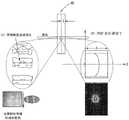
参考图4,该图例示了用于估计激光焊接结合区的物理范围的实验布置。继续参考图4,如前所述激光焊接两片Eagle

图5是断裂样品的显微图像。参考图5,所示的断裂样品的三维共聚焦显微图像说明本公开的实施方式的密封强度足够地强,使得通过撕开下面的基材(例如Eagle
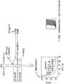
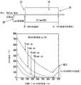
如在图3中注意到的,使用本公开的实施方式,利用示例性的低熔点膜或在入射波长下吸收/熔化的另一种膜,在膜和玻璃中形成色心以及在膜和玻璃中发生温度诱导的吸收可实现强的、气密性的透明结合。关于第一个判据,例如低熔点玻璃吸收事件,具有足够高的每单位面积功率的玻璃-LMG/UVA-玻璃结构的激光照射可以在溅射的薄膜LMG/UVA界面中引发吸收,从而引起熔化。图3左下角的底部曲线中易于观察到这一情况。底部曲线的第一斜坡跟踪LMG/UVA熔化过程约15秒,此时发生另一个过程,这一过程是相应基材中的玻璃-激光相互作用(即,色心形成)。在约17秒后,该中间向下曲线的大曲率能够表明由于玻璃中形成色心而发生了大的吸收。这些色心一般可根据基材中的元素杂质含量变化而变化,所述元素杂质例如As、Fe、Ga、K、Mn、Na、P、Sb、Ti、Zn、Sn等。透射曲线越弯曲,则形成的色心越多。这是在图3中提到的第二个判据。LMG/UVA膜的熔点可以为,但不限于约450℃,但是基于使用替代的涂覆有铝的EXG玻璃基材在类似的激光焊接条件下所进行的激光照射实验的观察情况,界面温度可能高于660℃。在该实验中,铝熔化(熔化温度:660℃),并且使用经过校准的热成像摄像机(FLIR摄像机)测量到使用激光焊接条件的表面温度为约250℃。As noted in FIG. 3 , using embodiments of the present disclosure, color centers are formed in films and glasses using an exemplary low melting point film or another film that absorbs/melts at incident wavelengths and in films and glasses. The temperature-induced absorption that occurs in the medium enables a strong, gas-tight transparent bond. Regarding the first criterion, such as low melting glass absorption events, laser irradiation of glass-LMG/UVA-glass structures with sufficiently high power per unit area can induce absorption in the sputtered thin-film LMG/UVA interface, thereby causing melt. This is easily observed in the bottom curve in the lower left corner of Figure 3. The first slope of the bottom curve traces the LMG/UVA melting process for about 15 seconds, at which point another process occurs, which is the glass-laser interaction (ie, color center formation) in the corresponding substrate. After about 17 seconds, the large curvature of the middle downward curve can indicate a large absorption due to the formation of color centers in the glass. These color centers can generally vary depending on the content of elemental impurities in the substrate, such as As, Fe, Ga, K, Mn, Na, P, Sb, Ti, Zn, Sn, and the like. The more curved the transmission curve, the more color centers are formed. This is the second criterion mentioned in Figure 3. The melting point of the LMG/UVA film may be, but is not limited to, about 450°C, but based on observations from laser irradiation experiments using an alternative aluminum-coated EXG glass substrate under similar laser welding conditions, the interface temperature may be higher than 660°C. In this experiment, aluminum was melted (melting temperature: 660°C), and the surface temperature using laser welding conditions was measured to be about 250°C using a calibrated thermal imaging camera (FLIR camera).
图6是根据本公开的一些实施方式所述的建模方案示意图。参考图6,利用LMG/UVA和EXG材料的热传输特性来模拟355nm激光以0.8–3kW/cm2撞击包含1μm薄无机膜+700μmEXG的两层堆叠件。在模型中未考虑无机薄膜(例如,LMG、IRA、UVA膜等)中的相变。继续参考图6,瞬态热分布的估计表明可获得大于660℃的界面温度。无论是否达到了高于660℃的确切的界面温度,热熔化的LMG/UVA界面膜的存在通过将能带隙转移到较低能量而增加了玻璃基材中的吸收。这些带隙改变一般应理解为是由于基材晶格的热膨胀所致,其与电子能的改变有关,以及与由于电子-光子相互作用引起的带能量直接重整化有关。图3的右下角示出了熔合二氧化硅中的这一性质的图。净效果是热的LMG/UVA膜通过降低带隙而在界面附近的EXG基材中促使了更多的吸收,这进而从内部转换过程产生了更多的热量,甚至使带隙进一步降低。这一过程可以统称为热诱导吸收,其表示图3指示的第三个判据。当然,在这些实施方式中可以使用其他无机膜,并且这些实例不应限制所附权利要求书的范围。6 is a schematic diagram of a modeling scheme according to some embodiments of the present disclosure. Referring to Figure 6, the thermal transport properties of LMG/UVA and EXG materials were used to simulate a 355 nm laser striking atwo -layer stack containing 1 μm thin inorganic film + 700 μm EXG at 0.8–3 kW/cm. Phase transitions in inorganic thin films (eg, LMG, IRA, UVA films, etc.) are not considered in the model. With continued reference to Figure 6, an estimate of the transient thermal distribution indicates that an interface temperature greater than 660°C can be obtained. Whether or not the exact interfacial temperature above 660°C is reached, the presence of the thermally melted LMG/UVA interfacial film increases absorption in the glass substrate by shifting the energy bandgap to lower energies. These bandgap changes are generally understood to be due to thermal expansion of the substrate lattice, which is related to changes in electron energy, as well as to direct renormalization of the band energy due to electron-photon interactions. A graph of this property in fused silica is shown in the lower right corner of FIG. 3 . The net effect is that the hot LMG/UVA film induces more absorption in the EXG substrate near the interface by lowering the bandgap, which in turn generates more heat from the internal conversion process and even lowers the bandgap further. This process can be collectively referred to as thermally induced absorption, which represents the third criterion indicated in FIG. 3 . Of course, other inorganic membranes may be used in these embodiments, and these examples should not limit the scope of the appended claims.
如上所述,色心形成在本公开实施方式的激光焊接形成中起到重要作用。使用图8所示的实验布置在图7中例示了在非多光子条件下对基本色心形成过程建模以基于三能级图(three level diagram)导出拟合函数。图7是根据本公开的实施方式所述的另一个建模方案。在图7的左图中,玻璃的三个电子带态吸收355nm光子,在基态ng[t]、导带ne[t]和色心ncc[t]中累积或消耗布居数(population)。应注意的是,单头箭头表示激光吸收,而双头箭头表示受激吸收和发射。在图7的右图中,提供了速率方程,其预测电子能级布居的平滑单调累积和消耗,而系统的相干驱动部分表现出相同布居的快速振荡

下面的方程(1)描述了实验可观察到的吸光度(Abs)与时间的关系,例如,与透射率(trans)对时间数据的关系有关:(1≈Abs+Trans)。解可以是上升和衰减指数的总和,但可以简化为以下表达式:Equation (1) below describes the experimentally observable absorbance (Abs) versus time, eg, transmittance (trans) versus time data: (1≈Abs+Trans). The solution can be the sum of the rising and decaying exponents, but can be simplified to the following expression:

其中α表示线性吸收系数(cm-1),I表示激光通量(光子/cm2·秒),σg表示基态吸收截面(cm2),σesa(σ激发)表示激发态吸收截面(cm2),σcc表示色心(color-enter)吸收截面(cm2),kec表示瞬态色心率,并且kf表示荧光衰减率。参考方程(1)和图8,可观察到色心形成在本公开实施方式中的作用。图9是根据本公开的一个实施方式所述的图。参考图9,对于某些非限制性激光-玻璃相互作用参数,在存在色心形成的情况下提供等式(1)的图(图示的弧线),以及在不存在色心形成的情况下提供等式(1)的图(图示的直线),所述激光-玻璃相互作用参数为α=0.01cm-1,I=4.6·10-21光子/cm2·秒,σg=1.20·10-17cm2,σesa=1.21·10-17cm2,σcc=2.20·10-13cm2,kec≈kf≈1.0·107秒-1。设置σcc=0,可以进行线性相关。然后通过以下关系:%透射率=100-%吸光度的关系得到%透射率。如图9所例示,由此可见,使用合理选择的参数值,简单地将色心形成项归零(即,设置σcc=0)将弧线变换为直线。实验用激光焊接玻璃基材通常表现出这种曲率,所述玻璃基材包括但不限于Eagle

图10提供了分析在玻璃界面处,从示例性LMG膜层进入到Eagle

图35C示出了密封装置200的截面图(例如沿着图35B中的线C截取)。如图所示,可以在密封之后形成焊接区域250,该焊接区域从第一基材210中的第一深度d1延伸到第二基材220中的第二深度d2。不希望囿于理论,认为焊接区域250可以表示组成与第一和第二基材210、220中的任一者和/或无机膜230不相同的区域。例如,由于基材和/或膜的粘弹性膨胀或溶胀,来自每层的各种元素可以从它们各自的各个层迁移出并进入到焊接区域250中,如关于图38A-C更详细地讨论的。例如,无机膜230可以包括一种或多种无机膜元素,例如F、P、Sn、B、Bi、Zn、Ti、W、Ce、Nb、Pb、Fe、Va、Cr、Mn、Mg或Ge,它们可以存在或不存在于第一和/或第二基材210、220中。同样地,第一和/或第二基材210、220可以包括一种或多种无机基材元素,例如Al、B、Si、Na、Li、K、Mg、Ca或Ba,它们可以存在或不存在于无机膜230中。这些膜和基材元素的迁移和混合可以产生化学组成与各个层不同的焊接区域。Figure 35C shows a cross-sectional view of the sealing device 200 (eg, taken along line C in Figure 35B). As shown, a
例如,在一些实施方式中,在激光密封期间,基材和/或无机膜可能由于吸收激光能而膨胀和变形,并且由于这种吸收而产生局部加热。热膨胀可以使一种或多种无机膜和基材元素迁移(不同于扩散),从而形成化学组成与各个部件不同的焊接区域250,所述化学组成例如来自第一基材210、无机膜230和/或第二基材220的元素混合物。焊接区域250可以存在于密封装置的焊接部分W中,例如,激光束入射在密封界面上的地方,从而在两个基材之间形成结合。焊接部分W可以构成连续的单条线,或者在其他实施方式中,一个或多个焊接部分W可以被非焊接部分I分开(例如,如图35C所示)。For example, in some embodiments, during laser sealing, the substrate and/or inorganic film may expand and deform due to absorption of laser energy and localized heating due to this absorption. Thermal expansion can migrate (as opposed to diffusion) one or more of the inorganic film and substrate elements to form a
根据各个实施方式,无机膜和基材元素迁移进和迁移出密封界面可以产生厚度tW大于无机膜的初始厚度的焊接区域250。例如,一个或多个膜元素可以在任一侧上从无机膜迁移到深度d1或d2,从而形成厚度tW=ti+d1+d2的焊接区域250,其中ti是无机膜厚度(未标记)。在该区域中,焊接区域的化学组成可以与无机膜和第一或第二基材不同,例如,由于一种或多种膜元素迁移到基材中和/或一种或多种基材元素迁移到无机膜中所致。根据各个实施方式,深度d1和d2可以相同或不同,并且例如,可以为约0.1μm至约2μm,例如约0.2μm至约1.8μm、约0.3μm至约1.6μm、约0.4μm至约1.5μm、约0.5μm至约1.4μm、约0.6μm至约1.2μm、或约0.8μm至约1μm,包括其间的所有范围和子范围。焊接区域250的厚度tW可以类似地变化,这取决于无机膜130的初始厚度以及膜和/或基材元素的迁移程度(例如,d1和d2的量值)。示例性的焊接厚度tW可包括但不限于0.3μm至约14μm,例如约0.5μm至约12μm、约0.8μm至约10μm、约1μm至约8μm、约2μm至约7μm、约3μm至约6μm或约4μm至约5μm,包括其间的所有范围和子范围。According to various embodiments, migration of the inorganic film and substrate elements into and out of the sealing interface can result in a
在一些实施方式中,焊接区域250的化学组成可以与非焊接部分I中的无机膜230和/或第一或第二基材210、220的化学组成不同。例如,焊接区域250可以具有第一无机基材元素浓度,其大于非焊接部分I中(例如参见区域Ii)无机膜230中的第二无机基材元素浓度。在其他实施方式中,焊接区域250可以具有第一无机膜元素浓度,其大于非焊接部分I中(例如参见区域S1i和S2i)的第一和/或第二基材210、220中的第二无机膜元素浓度。根据另外的实施方式,焊接区域250可以具有第一无机膜元素浓度,其大于焊接部分W中,但落在焊接区域250外(例如参见区域S1和S2)的第一和/或第二基材210、220中的第三无机膜元素浓度。在另外的实施方式中,焊接区域250中的第一和/或第二基材的一部分(例如参见区域S1W和S2W)可以具有第四无机膜元素浓度,其大于非焊接的I和/或焊接的W部分中(例如参见区域S1i和S2i和/或S1和S2)的第一和/或第二基材中的第二和/或第三无机膜元素浓度。In some embodiments, the chemical composition of the
图36A-B是分别是在激光焊接之前和之后的密封界面的SEM图像。在所示的实施方式中,第一和第二基材210、220包括

例如,取决于所用的材料和激光加工参数,上述区域各自之间的浓度差异可独自变化,并且在一些实施方式中,可在约5摩尔%至约80摩尔%的范围内,例如约10摩尔%至约75摩尔%、约15摩尔%至约70摩尔%、约20摩尔%至约65摩尔%、约25摩尔%至约60摩尔%、约30摩尔%至约55摩尔%、约35摩尔%至约50摩尔%、或约40摩尔%至约45摩尔%,包括其间的所有范围和子范围。在一些实施方式中,第一膜元素浓度可以比第二膜元素浓度高至少约5摩尔%(例如高至少约10、20、30、40、50、60、70或80摩尔%),并且/或者第一基材元素浓度可以比第二基材元素浓度高至少约30摩尔%(例如高至少约40、50、60、70或80摩尔%)。可以以本领域已知的各种方式测量这种组成差异,举例而言,例如二次离子束质谱(SIMS)、元素探针显微镜分析(EPMA)和过渡电子显微技术(TEM)。For example, depending on the materials used and laser processing parameters, the difference in concentration between each of the above regions can vary independently, and in some embodiments can range from about 5 mol % to about 80 mol %, such as about 10 mol % % to about 75 mol %, about 15 mol % to about 70 mol %, about 20 mol % to about 65 mol %, about 25 mol % to about 60 mol %, about 30 mol % to about 55 mol %, about 35 mol % % to about 50 mol %, or about 40 mol % to about 45 mol %, including all ranges and subranges therebetween. In some embodiments, the first film element concentration may be at least about 5 mole percent higher (eg, at least about 10, 20, 30, 40, 50, 60, 70, or 80 mole percent higher) than the second film element concentration, and/ Alternatively, the first substrate element concentration may be at least about 30 mole percent higher (eg, at least about 40, 50, 60, 70, or 80 mole percent higher) than the second substrate element concentration. Such compositional differences can be measured in various ways known in the art, such as, for example, secondary ion beam mass spectrometry (SIMS), elemental probe microscopy (EPMA), and transitional electron microscopy (TEM).
在密封期间或之后,还可以在装置中形成应力区域或热影响区域(HAZ)260,该应力区域从第一基材210中的第三深度d3延伸到第二基材220中的第四深度d4。如图35C所示,应力区域260可以涵盖或包括焊接区域250以及周围的区域(例如,区域S1S和S2S)。由此,焊接区域250外的第一和/或第二基材的部分仍然可以落入应力区域260内,无论是在装置的焊接的W部分还是非焊接的I部分中。在一些实施方式中,应力区域260的厚度tS可在几十微米至几百微米的范围内,例如,约20μm至约500μm,例如约30μm至约400μm、约40μm至约300μm、约50μm至约200μm、约60μm至约150μm、约70μm至约120μm、或者约80μm至约100μm,包括其间的所有范围和子范围。根据另外的实施方式,深度d3和d4可以相同或不同。During or after sealing, a stress zone or heat affected zone (HAZ) 260 may also be formed in the device, the stress zone extending from a third depth d3 in the
不希望囿于理论,但认为区域260中的残余应力可能因在焊接区域中或附近有激光暴露,使得基材迅速加热和冷却而存在。虽然激光可以在密封界面处聚焦于特定束斑直径,但是来自激光的热量可以散发并影响更大部分的密封装置,该更大部分延伸超过焊接区域250,例如,大到焊接区域外几十或几百微米。例如,取决于焊接温度和激光的停留时间,应力区域的尺寸可以变化。但是,即使是在高的平移速度下(例如停留时间<2-3ms),热扩散(1.4x10⁻⁶m2/s)可导致应力区大到几十微米。可以影响应力区的其他因素可包括由于玻璃基材中的色心吸收和/或玻璃的UV边缘位移而导致的基材的直接加热。Without wishing to be bound by theory, it is believed that residual stress in
在一些实施方式中,区域260中的应力可以与区域260外的密封装置中的应力不同。例如,区域260中(例如参见区域S1S)的一部分第一基材210可以具有第一应力,其大于区域260外(例如参见区域S1)的第一基材210中的第二应力。在其他实施方式中,区域260中(例如参见区域S2S)的一部分第二基材220可以具有第三应力,其大于区域260外(例如参见区域S2)的第二基材220中的第四应力。虽然在图36A-36B的SEM图像中不易见到具有可变应力的这些区域,但是每个区域的应力可使用下述任意方法进行定量和比较。In some embodiments, the stress in the
例如,取决于所用的材料和激光加工参数,上述区域各自之间的应力差异可独立变化,并且在一些实施方式中可在约1MPa至约25MPa或更高的范围内,例如约2MPa至约20MPa、约3MPa至约15MPa、约4MPa至约10MPa、约5MPa至约8MPa、或约6MPa至约7MPa,包括其间的所有范围和子范围。根据另外的实施方式,区域260中的应力相对于区域260外的应力的比值可以在约1.1:1至约25:1的范围内,例如约1.2:1至约20:1、约1.3:1至约15:1、约1.4:1至约10:1、约1.5:1至约9:1、约1.6:1至约8:1、约1.7:1至约7:1、约1.8:1至约6:1、约1.9:1至约5:1、约2:1至约4:1、或约2.5:1至约3:1,包括其间的所有范围和子范围。For example, depending on the material used and the laser processing parameters, the stress difference between each of the above regions can vary independently, and in some embodiments can range from about 1 MPa to about 25 MPa or higher, such as about 2 MPa to about 20 MPa , about 3 MPa to about 15 MPa, about 4 MPa to about 10 MPa, about 5 MPa to about 8 MPa, or about 6 MPa to about 7 MPa, including all ranges and subranges therebetween. According to further embodiments, the ratio of the stress in the
这些区域中的应力可通过各种技术来测量和/或估算,包括但不限于应力双折射(应力测试)、拉曼光谱法(假想温度和应力的变化)、布里渊(Brilluoin)光谱法(假想温度和应力的变化)、折射率测量(由于假想温度和应力引起的折射率变化)、偏振显微技术和/或热容量测量。根据各个实施方式,如果需要,在密封后,可以使密封装置进行一步或多步随后的退火步骤以降低和/或估算区域260中的应力。Stress in these regions can be measured and/or estimated by a variety of techniques including, but not limited to, stress birefringence (stress testing), Raman spectroscopy (change in hypothetical temperature and stress), Brilluoin spectroscopy (change in hypothetical temperature and stress), refractive index measurement (change in refractive index due to hypothetical temperature and stress), polarization microscopy and/or heat capacity measurement. According to various embodiments, after sealing, the sealing device may be subjected to one or more subsequent annealing steps to reduce and/or estimate stress in
虽然基于界面各材料之间明显大的CTE错配——CTE870CHM=18ppm/℃相比于CTEEXG=3.1ppm/℃,可能预计本公开实施方式中使用的可移动的原子物质具有显著更大的扩散,但是并没有观察到剥离。相反,反复循环高达600℃的温度似乎消除了任何残余应力,从而产生更强的结合。得到的无机薄膜足够地薄,使得由于各个玻璃基材的CTE错配导致的剥离力远小于结合力。这符合来自粘合膜沉积应力的层压结构复合应力与膜厚度的立方成比例的知识。Although based on the significantly larger CTE mismatch between the materials at the interface - CTE870CHM = 18 ppm/°C compared to CTEEXG = 3.1 ppm/°C, it may be expected that the mobile atomic species used in embodiments of the present disclosure have significantly larger diffusion, but no peeling was observed. Conversely, repeated cycling of temperatures up to 600°C appears to remove any residual stress, resulting in a stronger bond. The resulting inorganic films are thin enough that the peel force due to the CTE mismatch of the individual glass substrates is much smaller than the bond force. This is consistent with the knowledge that the composite stress of the laminate structure from the deposition stress of the adhesive film is proportional to the cube of the film thickness.
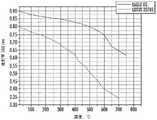
图11是在不同厚度的玻璃片之间的激光焊接性能的示意图。参考图11,发现将超薄Willow玻璃(0.1mm)焊接到Eagle
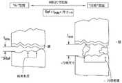
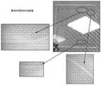
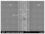
虽然此前的描述已经描述了将玻璃激光焊接到玻璃基材(具有相似或不同的尺寸、几何形状和/或厚度),但是这不应该限制本文所附权利要求书的范围,因为实施方式在具有或不具有导电性界面膜的情况下,同样可适用于非玻璃材料的基材或片材,例如但不限于陶瓷、玻璃陶瓷、金属等。例如,图12是估算在ITO引线上方的激光焊接范围的实验示意图。参考图12,在图12的左图中例示了经LMG涂覆的Eagle


图13提供了在ITO图案化膜上方形成的激光密封线的另外的照片。参考图13的左图,从不同来源获得另一种电极类型,其同样由ITO制成并且厚度为约250nm。ITO膜是连续的,使用本文所述的方法在其上形成密封。测量约10mm距离内的初始电阻为220欧姆。当从透明玻璃转到电极区域时,以恒定速度和功率进行激光密封。在进行密封后,在透明玻璃和ITO区域上方均观察到牢固的密封,并且ITO上方的密封略宽约10-15%。密封宽度的这种增加可能提示在该区域中产生的热多于在透明区域中产生的热。由于激光辐射使得电极材料吸收或者由于膜的不同热扩散性质也可以引起额外的热生成,并且在任何情况下,测量到电阻增加约10%达到240Ω,这是微不足道的。这也可以表明,当温度相对于空白玻璃升高时,较高质量的ITO和较厚的膜没有表现出导电性下降。应注意,当从透明玻璃转变到电极区域时,降低激光密封功率可以减少额外的热生成并因此使ITO的电阻率降低减少。实验结果还提示,当使用的电极宽度在激光束宽度的1/2-1/3之间,并且间距在光束直径的1/2-1/3之间时,在密封位置处分成电极阵列(具有与原始电极相同的总宽度)的单个电极可以是最佳的。后来以高于20mm/s的高密封速度进行的实验表明,在密封后,电阻下降<1-2%,其中初始电阻约为200Ω。Figure 13 provides additional photographs of laser seal lines formed over the ITO patterned film. Referring to the left image of Figure 13, another electrode type was obtained from a different source, again made of ITO and having a thickness of about 250 nm. The ITO film is continuous and a seal is formed thereon using the methods described herein. The initial resistance was measured to be 220 ohms over a distance of about 10mm. Laser sealing is performed at constant speed and power when going from the clear glass to the electrode area. After sealing, a firm seal was observed over both the clear glass and the ITO area, and the seal over the ITO was slightly wider by about 10-15%. This increase in seal width may suggest that more heat is generated in this area than in the transparent area. Additional heat generation can also be caused by absorption by the electrode material due to laser radiation or due to the different thermal diffusion properties of the film, and in any case an increase in resistance of about 10% to 240Ω was measured, which is negligible. It may also show that higher quality ITO and thicker films did not show a decrease in conductivity when the temperature was raised relative to the blank glass. It should be noted that reducing the laser encapsulation power can reduce the additional heat generation and thus the resistivity reduction of the ITO when transitioning from the transparent glass to the electrode area. The experimental results also suggest that when the electrode width used is between 1/2-1/3 of the laser beam width and the spacing is between 1/2-1/3 of the beam diameter, the electrode array is divided at the sealing position ( A single electrode with the same overall width as the original electrode) may be optimal. Later experiments at high sealing speeds above 20 mm/s showed that the resistance dropped <1-2% after sealing, with an initial resistance of about 200 Ω.
图14是在图案化膜上方形成的另外的激光密封线的一系列照片。参考图14,用不透明的钼金属电极进行类似的实验。图14提供了连续且图案化的钼界面膜的一系列照片,其显示出在该钼界面膜上形成了激光密封线。在左图中,连续钼膜的照片说明了具有裂纹或破裂的钼电极部分形成了更不均匀结合。即使在这种情况下,在恒定的激光密封功率下,均匀的钼电极也没有完全损坏。然而,由于均匀的电极吸收或反射激光辐射,电极区域的加热明显高于透明玻璃区域。这可以通过钼区域上方的密封区域的宽度增加来观察到。应该注意的是,未损坏的一个区域位于透明且均匀的钼区域之间的过渡区域,从而提示功率调整、激光功率密度、激光点速度或密封事件期间全部三个因素的组合可以克服任何过热对均匀的钼电极的影响。在图14的右图中,图案化或穿孔的钼膜的照片例示了形成了更均匀的结合,使得对其导电性的扰动程度最小,即焊接之前的14Ω到焊接后的16Ω。在该穿孔区域上方的密封表现出显著更少的热,因此提供了功率调制方法的替代方案。还应注意的是,应该仔细选择电极金属,因为已经发现,与钼或熔化温度高的其他金属相比,用熔化温度低的金属(Al)(650℃对比1200℃)来密封不太可能在密封条件下保持完好。因此,结果提示,当使用的电极宽度在激光束宽度的1/2-1/3之间,并且间距在光束直径的1/2-1/3之间时,在密封位置处分成电极阵列(具有与原始电极相同的总宽度)的单个电极可以是最佳的。因此,本公开的实施方式可适用于玻璃与玻璃、金属、玻璃陶瓷、陶瓷和具有相同或不同尺寸、几何形状和厚度的其他基材的激光密封。Figure 14 is a series of photographs of additional laser seal lines formed over the patterned film. Referring to Figure 14, a similar experiment was performed with an opaque molybdenum metal electrode. Figure 14 provides a series of photographs of a continuous and patterned molybdenum interfacial film showing the formation of laser seal lines on the molybdenum interfacial film. In the left panel, the photograph of the continuous molybdenum film illustrates that the molybdenum electrode portion with cracks or fractures forms a more inhomogeneous bond. Even in this case, under constant laser sealing power, the uniform molybdenum electrode was not completely damaged. However, the heating of the electrode area is significantly higher than that of the transparent glass area due to the uniform electrode absorption or reflection of the laser radiation. This can be observed by the increased width of the sealing region above the molybdenum region. It should be noted that one area that was not damaged is located in the transition area between the transparent and uniform molybdenum areas, suggesting that power adjustment, laser power density, laser spot speed, or a combination of all three factors during the sealing event can overcome any overheating effect. The effect of a uniform molybdenum electrode. In the right panel of Figure 14, a photograph of a patterned or perforated molybdenum film illustrates the formation of a more uniform bond with minimal disturbance to its conductivity, ie 14Ω before soldering to 16Ω after soldering. Sealing over this perforated area exhibits significantly less heat, thus providing an alternative to power modulation methods. It should also be noted that the electrode metal should be chosen carefully, as it has been found that sealing with a metal with a low melting temperature (Al) (650°C vs. 1200°C) is less likely than molybdenum or other metals with a high melting temperature Remains intact under sealed conditions. Therefore, the results suggest that when the electrode width used is between 1/2-1/3 of the laser beam width and the spacing is between 1/2-1/3 of the beam diameter, the electrode array is divided at the sealing position ( A single electrode with the same overall width as the original electrode) may be optimal. Accordingly, embodiments of the present disclosure may be applicable to laser sealing of glass to glass, metal, glass-ceramic, ceramic, and other substrates of the same or different sizes, geometries, and thicknesses.
可利用本文所述实施方式的应用有效地形成结合强度高、透明、玻璃与玻璃的焊接,这样的应用很多,包括但不限于固态照明、显示器和透明真空绝缘技术。特别地,玻璃的激光焊接可以提供许多传统焊接方法(例如电子束、电弧、等离子体或焰炬)根本不能提供的一些效率和特征,例如小的热影响区(HAZ)。在一些实施方式中,对于许多玻璃是不透明的情况,激光玻璃焊接一般可以在没有预加热或后加热的情况下使用红外(IR)激光器进行;或者对于许多玻璃是透明的情况,激光玻璃焊接可以在没有预加热或后加热的情况下使用超短脉冲激光器(USPL)进行。在一些实施方式中,正确地选择玻璃基材组合物和分布于界面的IR吸收玻璃料可以得到气密的“夹层型”玻璃激光密封封装件。在一些实施方式中,超短脉冲激光可以聚焦在示例性玻璃基材中的表面或内部点处,并且可以通过非线性过程(例如多光子或雪崩电离)诱导吸收。High bond strength, transparent, glass-to-glass welds can be effectively formed utilizing the applications of the embodiments described herein, many of which include, but are not limited to, solid state lighting, displays, and transparent vacuum insulation technologies. In particular, laser welding of glass can provide efficiencies and features, such as a small heat-affected zone (HAZ), that many conventional welding methods (eg, electron beam, arc, plasma, or torch) simply cannot. In some embodiments, where many glasses are opaque, laser glass welding can generally be performed using an infrared (IR) laser without pre- or post-heating; or, where many glasses are transparent, laser glass welding can It was performed using an ultrashort pulse laser (USPL) without preheating or postheating. In some embodiments, proper selection of the glass substrate composition and the IR absorbing frit distributed at the interface can result in a hermetic "sandwich type" glass laser sealed package. In some embodiments, ultrashort pulsed laser light can be focused at a surface or internal point in an exemplary glass substrate, and absorption can be induced by nonlinear processes such as multiphoton or avalanche ionization.
至此,已经描述了低功率激光焊接工艺,其依赖于低熔点玻璃界面膜的吸收,并且由于其是低温结合形成(低至熔化温度的一半)以及对接触和压力条件的要求,因此,可归因于扩散焊接。如上所述,激光焊接玻璃片以及强的结合形成具有一些显著效果,例如,在入射激光波长下低熔点玻璃膜吸收,在玻璃基材中形成激光诱导的色心,以及在基材中发生了热诱导吸收有效地加速了温度的升高。So far, a low-power laser welding process has been described that relies on the absorption of a low-melting glass interfacial film, and due to its low-temperature bond formation (down to half the melting temperature) and the requirements for contact and pressure conditions, can be attributed due to diffusion welding. As mentioned above, laser welding of glass sheets and strong bond formation has some notable effects, such as low melting point glass film absorption at incident laser wavelengths, laser-induced color centers in the glass substrate, and occurrence of Thermally induced absorption effectively accelerates the temperature increase.
但是,在一些实施方式中,许多在入射波长(例如355nm)下高度吸收的膜足以诱导形成高结合强度的激光焊接。其他膜,例如ZnO或SnO2在化学上不同于本文所述的一些示例性低熔点玻璃组合物,但是在相对较低的光通量下同样具有相同的激光焊接能力。因此,与一些低熔点玻璃组合物(~450℃)相比,鉴于ZnO的熔化温度(1975℃),发现在一些实施方式中低熔化特征可能不是必需的。然而,发现这些膜的共同特征是它们基本上在355nm下吸收辐射:ZnO吸光度~45%(200nm厚的膜),低熔点玻璃~15%(200nm厚的膜)。还确定的是,本文所述的示例性方法可以对石英或纯的熔合二氧化硅基材——即没有色心的基材进行激光焊接。因此,已经确定的是,色心不一定是必需的,但是在一些实施方式中,当示例性的膜的吸收较低时(例如,~Abs<20%)可能需要色心。However, in some embodiments, many films that are highly absorbing at incident wavelengths (eg, 355 nm) are sufficient to induce high bond strength laser welds. Other films, such as ZnO orSnO2 , are chemically different from some of the exemplary low melting point glass compositions described herein, but also have the same laser weldability at relatively lower flux. Therefore, in view of the melting temperature of ZnO (1975°C) compared to some low melting glass compositions (-450°C), it was found that the low melting feature may not be necessary in some embodiments. However, it was found that a common feature of these films is that they absorb radiation substantially at 355 nm: ZnO absorbance -45% (200 nm thick film), low melting glass -15% (200 nm thick film). It has also been determined that the exemplary methods described herein can laser weld quartz or pure fused silica substrates, ie, substrates without color centers. Thus, it has been determined that color centers are not necessarily required, but may be desired in some embodiments when the absorption of the exemplary films is low (eg, ~Abs<20%).
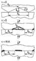
图15是根据一些实施方式所述的另一种方法的简化图。参考图15,具有限定的光束宽度或直径D的散焦激光15入射在由两片玻璃17、18接触形成的夹层型结构16上,其中一片的内部界面涂有薄的吸收膜19。虽然所示的光束为圆柱形,但是这种描绘不应限制本文所附权利要求书的范围,因为光束可以是圆锥形或其他合适的几何形状。可以针对入射激光波长下的吸光度来选择膜材料。激光15可以以预定的速度Vs平移,并且激光束的平移时间可以有效地照射给定点,并且可以通过停留时间D/Vs来表征。在一些实施方式中,可以在焊接或结合事件期间施加适度的压力,以确保清洁表面之间持续接触,同时调整任何一个或多个参数以优化焊接。示例性的非限制性参数包括激光功率、速度Vs,重复频率和/或束斑直径D。15 is a simplified diagram of another method according to some embodiments. Referring to Figure 15, a defocused
如上文关于图3所述,发现最佳焊接可以是三种机制的函数,即,通过示例性膜和/或基材吸收激光辐射以及基于该吸收过程的加热效应;增加由于加热效应(带隙向较长波长位移)引起的膜和基材吸收,其可以是瞬态的并且取决于加工条件;以及由UV辐射产生的缺陷或杂质吸收或色心吸收。热分布可以是该过程的重要方面,下文的论述可以用于帮助理解在两个基材之间的界面处的温度分布,假设界面处是静态吸收。As described above with respect to Figure 3, it was found that optimal welding can be a function of three mechanisms, namely, absorption of laser radiation by exemplary films and/or substrates and heating effects based on this absorption process; increased due to heating effects (bandgap Shift to longer wavelengths) induced film and substrate absorption, which can be transient and depend on processing conditions; and defect or impurity absorption or color center absorption resulting from UV radiation. Heat distribution can be an important aspect of the process, and the discussion below can be used to help understand the temperature distribution at the interface between two substrates, assuming static absorption at the interface.
El-Adawi开发了一种分析模型,其用于分析在大型半无限平板基材上激光加热由厚度为Z的吸收膜组成的双层堆叠件。使用匹配的边界条件求解每种材料中的热扩散方程,得到作为膜与基材的时间和位置的函数的温度表达:Tf(t,z),Ts(t,z)。El-Adawi的模型假定膜和基材的热性质(扩散率D、热导率k、热容量Cp)是固定的,使得仅在表面中发生吸收并且没有发生相变。使用拉普拉斯变换(Laplace transforms)产生具有指数和误差(互补)函数项的求和:El-Adawi developed an analytical model for the laser heating of a bilayer stack consisting of an absorbing film of thickness Z on a large semi-infinite slab substrate. Solving the thermal diffusion equation in each material using matched boundary conditions yields a temperature expression as a function of time and position of the film and substrate: Tf (t,z), Ts (t,z). El-Adawi's model assumes that the thermal properties of the film and substrate (diffusivity D, thermal conductivity k, heat capacity Cp) are fixed such that absorption occurs only in the surface and no phase transition occurs. Use Laplace transforms to produce a summation with exponential and error (complementary) function terms:

其中Af表示薄膜的表面吸光度,Io表示激光通量(光子/cm2·秒),n表示整数(0≤n≤∞),所有下标f表示膜参数,而下标s表示基材参数。B和ε与材料性质有关:B=1-ε/1+ε<1,ε=(ks/kf)√Df/Ds),同时Lf还包括时间t:

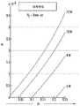
图16是相同实施方式的两层激光加热表面吸收模型。参考图16,该图示出了脉冲UV(355nm)激光20撞击具有1μm UV吸收膜23和700μm Eagle-XG基材24的双层堆叠件22。远离Eagle-XG堆叠件22中的焊接界面的空间温度分布可以从等式(2)计算出来并且绘制图,假设脉冲(30kHz,10ns脉冲宽度,500μm宽激光束腰直径)355nm激光的平均功率为6瓦特。然后采用不同的激光扫掠速度(2mm/s、5mm/s、10mm/2和20mm/s)。采用15%的UV膜吸光度来进行计算,该值是锡氟磷酸盐LMG材料在355nm下并且厚度为约200nm时的典型吸光度。因为与移动较快的光束相比,移动缓慢的激光束在给定的激光焊接位点上方停留得更久,因此,绘制Eagle
如图17所示,还研究了由于采用不同的激光功率,或者采用吸光度不同的膜而引起的温度变化。图17是一些实施方式的一系列温度变化图。参考图17,使用双层激光加热模型[方程(2)]绘制玻璃基材温度分布对激光功率和膜吸光度的依赖性。图17使用与图16相同的激光参数。更具体而言,使用具有以下参数的脉冲UV激光:λ=355nm,束腰=500μm,重复频率=30,000Hz以及脉冲宽度=10ns。如在图17的左图中可以观察到的,与图17的右图中的吸光度的高阶性质相比,激光功率对基材温度分布的影响似乎更加线性。这种性质在功率Io和吸光度Af出现耦合的方程(2)中不明显。吸光度可间接影响有效膜厚度zf,吸光度在某种程度上与膨胀系数bn和gn相关。相反,Io是独立的,其不存在与膨胀系数bn和gn相关的函数关系。As shown in Figure 17, the temperature change due to the use of different laser powers, or the use of films with different absorbances, was also investigated. Figure 17 is a series of temperature change graphs for some embodiments. Referring to Figure 17, the dependence of the glass substrate temperature distribution on laser power and film absorbance was plotted using a bilayer laser heating model [equation (2)]. Figure 17 uses the same laser parameters as Figure 16. More specifically, a pulsed UV laser with the following parameters was used: λ=355 nm, beam waist=500 μm, repetition frequency=30,000 Hz, and pulse width=10 ns. As can be observed in the left panel of Figure 17, the effect of laser power on the substrate temperature distribution appears to be more linear than the higher order nature of absorbance in the right panel of Figure 17. This property is not evident in equation (2) where power Io and absorbance Af appear coupled. The effective film thickness zf can be indirectly affected by absorbance, which is related to the expansion coefficientsbn and gn to some extent. In contrast, Io is independent, and there is no functional relationship related to the expansion coefficients bn and gn .
图18是针对一些实施方式的,在扫掠激光的停留时间内沉积的一系列平均能量图。参考图18,可以观察到停留时间同时取决于激光扫掠速度和激光脉冲重复频率,其数值和单位在独立变量x-y平面中表示出。这些计算假设膜吸光度为25%,激光束宽度为500微米和以及激光脉冲宽度为10ns——在一些实施方式中可以获得有成效的激光玻璃焊接。图18用所示平面表示并根据实验凭经验估算出了阈值功率(11a为6W,12a为20W),其高于产生有成效的激光焊接的功率。顶部和底部的曲线图或图使用的激光功率量不同:6瓦特对比20瓦特。图18中的两个图的比较表明,在低入射激光功率(例如,6瓦特)下,激光速度和重复频率的轻微变化可以产生比引起足够的激光焊接所需的入射功率显著更高的入射功率。即使重复频率更高而与初始激光焊接条件(30kHz,2mm/s激光扫掠速度)略微不同也会导致不必要的入射功率密度。更高的激光扫掠速度迅速导致对玻璃基材进行激光焊接所需的能量不足,这是激光停留时间与速度的反比关系对比激光停留时间与激光重复频率的线性关系的结果。在更高的入射激光功率(例如20瓦特)下,可获得较大的平台区域或工艺窗口11b、12b,其中速度和重复频率的微小偏移维持了充足的激光焊接条件而不会产生过多的能量。两个图的工艺窗口11b、12b可以有利于激光焊接或结合优化。Figure 18 is a series of plots of average energy deposited over the dwell time of the swept laser for some embodiments. Referring to Fig. 18, it can be observed that the dwell time depends on both the laser sweep speed and the laser pulse repetition frequency, the value and units of which are represented in the independent variable x-y plane. These calculations assume a film absorbance of 25%, a laser beam width of 500 microns and a laser pulse width of 10 ns - effective laser glass welding can be achieved in some embodiments. Figure 18 is represented by the plane shown and empirically estimated threshold power (6W for 11a and 20W for 12a), which is higher than the power to produce a productive laser weld. The top and bottom graphs or graphs use a different amount of laser power: 6 watts vs. 20 watts. A comparison of the two graphs in Figure 18 shows that at low incident laser powers (eg, 6 watts), slight changes in laser speed and repetition rate can produce significantly higher incident powers than required to cause adequate laser welding power. Even a higher repetition rate slightly different from the initial laser welding conditions (30 kHz, 2 mm/s laser sweep speed) results in unwanted incident power density. Higher laser sweep speeds rapidly lead to insufficient energy required for laser welding of glass substrates, a result of the inverse relationship of laser dwell time to speed versus the linear relationship of laser dwell time to laser repetition rate. At higher incident laser powers (eg, 20 watts), larger plateau areas or
图19是在用IR辐射源加热期间,在355nm下的Eagle


图20是一些实施方式在加热期间在355nm下的玻璃透射率图。参考图20,发现可以在膜和玻璃基材中发生由UV辐射引起的色心形成,这可以导致在辐射区域中具有额外吸收。由于结果使温度升高,在图20中可以观察到355nm透射对Eagle

图21是一些实施方式在UV辐射期间和之后,对膜和基材的透射率影响图。参考图21,第一曲线30表示具有200nm ZnO膜的Eagle
图22是一些实施方式的吸收相对于波长关系的图。参考图22,一个实施方式包括用基于FeO的玻璃制成的膜,根据加工条件,该膜可以处于两种不同的氧化态——2+和3+。该示例性的非限制性基于二氧化硅的玻璃膜具有大于约10-15重量%的FeO,其等比例为FeO和Fe2O3。如图22所例示的,发现Fe2O3在NIR波长下表现出强吸收,并且在1064nm的波长下还可用YAG激光照射。在这种情况下,可见光透射率小于约0.02并且不会损害在约420nm至约700nm之间的衰减。发现在1064nm下的吸收约为0.1,并且可以用高于示例性膜熔点的足够的激光功率加热示例性膜并进行激光焊接。当然,本文所附权利要求书不应限于此,因为还设想了IR吸收膜和其他IR激光的其他实例。Figure 22 is a graph of absorption versus wavelength for some embodiments. Referring to Figure 22, one embodiment includes a film made with FeO-based glass, which can be in two different oxidation states - 2+ and 3+ - depending on processing conditions. The exemplary non-limiting silica-based glass film has greater than about 10-15 wt % FeO in equal proportions FeO and Fe2O3. As exemplified in Figure 22, Fe2 O3 was found to exhibit strong absorption at NIR wavelengths and was also irradiable with YAG laser at a wavelength of 1064 nm. In this case, the visible light transmittance is less than about 0.02 and attenuation between about 420 nm and about 700 nm is not compromised. The absorption at 1064 nm was found to be about 0.1, and the exemplary films could be heated and laser welded with sufficient laser power above the melting point of the exemplary films. Of course, the claims appended hereto should not be so limited, as other examples of IR absorbing films and other IR lasers are also contemplated.
图23是在Eagle
图24是在Eagle


图25是一些实施方式在激光焊接时观察到的界面接触几何范围示意图。参考图25,左图表示在“Ra”范围内发生的界面条件,其中间隙t间隙的厚度由局部表面粗糙度决定,其统计特征在于Ra数,并且粗糙体的面内空间分布以部分相关长度为特征。图25的右图表示在“污物”范围内发生的界面条件,其中间隙t间隙的厚度由主要的污物粒径分布的统计学决定,并且面内空间分布由污物密度分布决定。因此,可以观察到Ra范围内的间隙厚度取决于玻璃基材表面统计学,范围从低至零点几纳米(例如,结晶范围)的超光滑数值到表示商购玻璃(例如,钠钙玻璃、硼硅酸盐玻璃)的典型数值几十纳米的上限。25 is a schematic illustration of the geometric range of interfacial contact observed during laser welding for some embodiments. Referring to Figure 25, the left panel represents the interfacial conditions occurring in the "Ra" range, where the thickness of thegap , t, is determined by the local surface roughness, which is statistically characterized by the Ra number, and the in-plane spatial distribution of the roughness is determined by the partial correlation length. as characteristic. The right panel of Figure 25 represents the interface conditions occurring in the "dirt" range, where the thickness of the gap tgap is determined by the statistics of the dominant dirt particle size distribution, and the in-plane spatial distribution is determined by the dirt density distribution. Thus, it can be observed that gap thicknesses in the Ra range are dependent on glass substrate surface statistics, ranging from ultra-smooth values as low as a few tenths of a nanometer (eg, the crystalline range) to values representing commercially available glasses (eg, soda lime glass, boron Typical values for silicate glass) are in the upper tens of nanometers.
探索激光焊接动力学、扩散焊接蠕变流动的潜在机制,可以观察到在低至玻璃基材的熔化温度的一半的温度下发生相对低温的结合形成,并且在一些实施方式中可能需要接触和压力条件。大部分基材材料质量传输到间隙中的方式与通过高于基材应变点的温度来激活的热溶胀膨胀玻璃一致。如下文更详细论述的,基材的粘弹性膨胀和溶胀可导致焊接区域富含一种或多种无机基材元素(例如参见图39A-C)。Exploring the kinetics of laser welding, the underlying mechanism of creep flow in diffusion welding, it was observed that relatively low temperature bond formation occurs at temperatures as low as half the melting temperature of the glass substrate, and may require contact and pressure in some embodiments condition. The manner in which most of the mass of the substrate material is transferred into the gap is consistent with thermally swellable expanded glass activated by a temperature above the strain point of the substrate. As discussed in more detail below, viscoelastic expansion and swelling of the substrate can cause the weld zone to be enriched with one or more inorganic substrate elements (see, eg, Figures 39A-C).
这种材料的移动可以通过扩散焊接模型中常见的各种形式的蠕变流动(即粘性过程、塑性过程或扩散传输过程)中的一种来描述。虽然这些模型常用于描述金属焊接,但是使用相对接触区域Ac/A0的概念,它们可用于本公开的情况,图26例示了其动力学发展情况。图26是在施加的恒定压力P外下,在对界面间隙区域进行激光焊接期间,相对接触区域Ac/A0的演变示意图。参考图26,在顶部的图中,时间=0并且相对接触区域Ac/A0的初始条件等于0。在中间的图中,时间大于0,其例示了界面间隙区域的中间状态,其中Ac/A0>0。在底部的图中,时间是预定点(t≈终点),此时已经基本上完成焊接或结合并且间隙实际上不存在,Ac/A0≈1。形成由图26所代表的扩散焊接界面假设相对接触面积Ac/A0的演变收敛到化学键形成的距离。可以用近似法来描述这些动力学:The movement of this material can be described by one of the various forms of creep flow (i.e. viscous, plastic, or diffusive transport processes) commonly found in diffusion welding models. While these models are commonly used to describe metal welding, using the concept of relative contact areaAc /A0 , they can be used in the context of the present disclosure, the kinetic development of which is illustrated in FIG. 26 . Figure 26 is a schematic diagram of the evolution of the relative contact areaAc /A0 during laser welding of the interfacial gap area underan applied constant pressure P. Referring to Figure 26, in the top graph, time=0 and the initial condition of the relative contact areaAc /A0 is equal to 0. In the middle plot, the time is greater than 0, which exemplifies the intermediate state of the interfacial gap region, where Ac /A0 >0. In the bottom graph, the time is the predetermined point (t ≈ end point) when the welding or bonding has been substantially completed and the gap is practically non-existent, Ac /A0 ≈1. Formation of the diffusion welded interface represented by Figure 26 assumes that the evolution of the relative contact areaAc /A0 converges to the distance of chemical bond formation. These dynamics can be described by approximation:

其中k表示常数,p表示压力,n表示压力指数,Q表示特定速率控制的蠕变流动机制的活化能。n值可如下与速率控制机制相关:对于粘性质量传输,n=1;对于塑性流动,n=2;对于蒸发/冷凝传输,n=3;并且对于扩散传输,n>3。where k is the constant, p is the pressure, n is the pressure exponent, and Q is the activation energy of the specific rate-controlled creep flow mechanism. The value of n can be related to the rate control mechanism as follows: n=1 for viscous mass transport; n=2 for plastic flow; n=3 for evaporation/condensation transport; and n>3 for diffusive transport.
方程(4)可用于指导推导起作用的某些机械力,因为表达式假定的是等温条件。为了开始这种机械研究,并且由于低软化点硼硅酸盐玻璃与Eagle


即使假设将温度固定在950℃,仍可以注意到在该条件下的粘性流动机制是否足以形成并促使扩散焊接完成(Ac/A0≈1)。图28提供了对这种情况的一些见解。图28是提供了针对一些实施方式估算的焊接速率比较情况的一系列图。参考图28,可以基于方程(4),使用低应变和低软化点硼硅酸盐玻璃蠕变流动参数和600MPa的有效焊接压力来对焊接速率估算值进行比较。这两个图的区别仅在于假设的是粘性流动(左图)还是塑性流动(右图)。回想约0.25秒的停留时间在约6瓦特和30kHz激光重复频率条件下产生了牢固的激光焊接,粘性流动解释可能受到质疑,图28中的左图表明了其他机制,例如塑性流动,这也可能是牢固的焊接形成的原因。Even assuming that the temperature is fixed at 950°C, it can be noted whether the viscous flow mechanism under this condition is sufficient to develop and promote the completion of the diffusion welding (Ac /A0 ≈ 1). Figure 28 provides some insight into this situation. 28 is a series of graphs that provide a comparison of estimated weld rates for some embodiments. Referring to Figure 28, welding rate estimates can be compared based on equation (4) using low strain and low softening point borosilicate glass creep flow parameters and an effective welding pressure of 600 MPa. The two graphs differ only in whether viscous flow (left graph) or plastic flow (right graph) is assumed. Recalling that a dwell time of about 0.25 seconds produced a strong laser weld at about 6 watts and a 30 kHz laser repetition rate, the viscous flow interpretation may be questioned, the left panel in Figure 28 suggests other mechanisms, such as plastic flow, which may also be is the reason for the formation of strong welds.
图29是一些实施方式的偏振测量和图像的示意图。参考图29,可以检查由在界面焊接结合附近进行的示例性激光焊接工艺产生的残余应力场。例如,图29的顶部图例示了在两个0.7mm Eagle

其中,除了Z代表熔化前沿位置,QL代表熔化潜热,并且热流为在表面处吸收的一维、光学辐射,以及热材料性质保持与温度无关外,各术语与方程(2)中使用的相同。然后可以以Z和dZ/dt导出二次方程,所述Z和dZ/dt具有作为热物理和激光参数的函数的系数。为了理解蔓延应力场的依赖性,可以通过将


其中Z表示蠕变前沿位置,l表示基材厚度,Cp表示基材热容,A表示基材吸光度,R表示基材反射率,ΔTm表示维持蠕变流所需的蔓延温度从环境温度升高情况(例如,ΔTm=T应变–T环境),ρ表示基材密度,λ表示基材热导率,Io表示激光辐照度(W/m2)以及t表示时间。where Z is the creep front position, l is the thickness of the substrate, Cp is the heat capacity of the substrate, A is the absorbance of the substrate, R is the reflectance of the substrate, ΔTm is the creep temperature required to maintain the creep flow from ambient temperature For the high case (eg, ΔTm = Tstrain - Tambient ), p represents substrate density, λ represents substrate thermal conductivity, Io represents laser irradiance (W/m2 ) and t represents time.
图30例示了功率依赖性,由此可以观察到,在焊接期间简单地增加激光功率可以在界面区域之外产生更大的应力,其中过量的能量导致形成了更大的应力。图30是根据示例性焊接线提供应力位置的图。参考图30,可以利用方程(6)确定来自示例性焊接线的应力位置,其中所采用的参数类似于先前使用的参数:波长=355nm,束腰=500μm,重复频率=30,000Hz,脉冲宽度=10ns,Vs=2mm/秒,停留时间=0.25秒,

图32是一些实施方式的示意图。参考图32,该图例示了利用吸收薄膜实现激光焊接的一种示例性非限制性方法,其中激光热能可以被传送到基材/基材界面40中以获得扩散结合相对接触区域,在预定时间内尽可能接近统一,同时最大程度地减少任何附带损坏,例如残余拉伸应力的空间范围和量值。对于焊接界面形成速率比CTE错配应力界面形成得更快的CTE较高的基材,该方法的作用可能更显著。因此,在一些实施方式中,可以在焊接界面处使用聚焦光束以及更高速度的扫掠速率,以实现示例性焊接而没有任何裂纹形成。Figure 32 is a schematic diagram of some embodiments. Referring to Figure 32, this figure illustrates an exemplary non-limiting method of laser welding utilizing an absorbing film in which laser thermal energy may be delivered into the substrate/
在一些实施方式中,激光焊接可使用在入射激光波长λ下吸收(优选A%>约20%)的膜来实现。在其他实施方式中,基材和膜在λ下均可表现出色心形成。在另外的实施方式中,温度影响可用于增加膜和基材中的一者或两者在λ下的吸收。这种示例性温度影响还可以有助于改进密封或焊接速度,并且可以减少热影响区(HAZ)并且可以降低蠕变流动的活化能,例如形成共晶系统、合金等。在一些实施方式中,如果需要透明度,则可以在UV中提供带隙,或在NIR、IR中提供高吸收。另外的实施方式可提供界面表面能γ焊接界面>>残余γ应力场和/或总积分结合强度
虽然已经描述了一些实施方式使用低熔点玻璃或无机膜,但是本文所附权利要求书不应限于此,因为实施方式可使用UV吸收膜、IRA膜和/或位于两个基材之间的其他无机膜。如上所述,在一些实施方式中,示例性基材玻璃中的色心形成不是必需的,并且随着膜的UV吸收(例如小于约20%)变化而变化。因此,在其他实施方式中,如果膜的UV吸收大于约20%,则替代性基材,例如石英、低CTE基材等易于形成焊接。此外,当使用高CTE基材时,这些基材易于利用示例性的高重复频率激光(例如,大于约300kHz至约5MHz)和/或低峰值功率来焊接。此外,在膜的吸收是影响因素的实施方式中,可以使用示例性IR激光系统来焊接IR吸收(可见光透明膜)。Although some embodiments have been described using low melting point glass or inorganic films, the claims appended hereto should not be so limited as embodiments may use UV absorbing films, IRA films and/or other films located between the two substrates Inorganic film. As noted above, in some embodiments, color center formation in the exemplary substrate glass is not required and varies as the UV absorption of the film (eg, less than about 20%) varies. Thus, in other embodiments, alternative substrates, such as quartz, low CTE substrates, etc., are susceptible to solder formation if the UV absorption of the film is greater than about 20%. Furthermore, when high CTE substrates are used, these substrates are easily welded using exemplary high repetition rate lasers (eg, greater than about 300 kHz to about 5 MHz) and/or low peak powers. Additionally, in embodiments where the absorption of the film is a contributing factor, an exemplary IR laser system can be used to weld IR absorption (visible light transparent films).
在本公开的各个实施方式中,玻璃密封材料和得到的各层是透明和/或半透明的、薄的、不可渗透的、“绿色的”,并且被构造成在低温下形成气密性密封,并且具有足够的密封强度以适应密封材料与相邻基材之间的大的CTE差。在一些实施方式中,密封层可以不含填料和/或粘合剂。用于形成密封层的无机材料可以不是基于玻璃料的,或者在一些实施方式中,可以是由研磨的玻璃形成的粉末(例如UVA、LMG等)。在其他实施方式中,密封层材料是在预定波长下具有基本光学吸收截面的低Tg玻璃,所述预定波长与用于密封工艺的激光的工作波长匹配或基本上匹配。在另外的实施方式中,在室温下,低Tg玻璃层对激光加工波长的吸收至少为15%。In various embodiments of the present disclosure, the glass encapsulant and resulting layers are transparent and/or translucent, thin, impermeable, "green" and configured to form a hermetic seal at low temperatures , and has sufficient seal strength to accommodate large CTE differences between the seal material and the adjacent substrate. In some embodiments, the sealing layer may be free of fillers and/or binders. The inorganic material used to form the sealing layer may not be frit based, or in some embodiments, may be a powder formed from ground glass (eg, UVA, LMG, etc.). In other embodiments, the sealing layer material is a low Tg glass having a substantial optical absorption cross-section at a predetermined wavelength that matches or substantially matches the operating wavelength of the laser used for the sealing process. In further embodiments, the low Tg glass layer absorbs at least 15% of the laser processing wavelength at room temperature.
一般来说,合适的密封剂材料包括低Tg玻璃和具有适当反应性的铜或锡的氧化物。玻璃密封材料可以由低Tg材料形成,例如磷酸盐玻璃、硼酸盐玻璃、亚碲酸盐玻璃和硫属化物玻璃。如本文所限定的,低Tg玻璃材料的玻璃化转变温度低于400℃,例如低于350℃、300℃、250℃或200℃。示例性硼酸盐玻璃和磷酸盐玻璃包括锡磷酸盐玻璃、锡氟磷酸盐玻璃和锡氟硼酸盐玻璃。溅射靶可以包括此类玻璃材料,或者,其前体。示例性的铜和锡氧化物是CuO和SnO,其可以由包括这些材料的压制粉末的溅射靶形成。任选地,玻璃密封组合物可包含一种或多种掺杂剂,包括但不限于钨、铈和铌。如果包含这些掺杂剂,则它们可对例如玻璃层的光学性质产生影响,并且可用于控制玻璃层对激光辐射的吸收。例如,掺杂二氧化铈可增加低Tg玻璃阻挡层在激光加工波长下的吸收。其他合适的密封剂材料包括液相线温度小于或等于约1000℃、小于或等于约600℃或者小于或等于约400℃的具有激光吸收的低液相线温度(LLT)材料。在其他实施方式中,可对无机膜的组成进行选择以降低诱导上述第一基材、第二基材或者第一和第二基材蠕变流动的活化能。In general, suitable encapsulant materials include low Tg glass and appropriately reactive copper or tin oxides. The glass sealing material may be formed from low Tg materials such as phosphate glass, borate glass, tellurite glass, and chalcogenide glass. As defined herein, the glass transition temperature of the low Tg glass material is below 400°C, eg, below 350°C, 300°C, 250°C or 200°C. Exemplary borate and phosphate glasses include tin phosphate glass, tin fluorophosphate glass, and tin fluoroborate glass. Sputtering targets may include such glass materials, or, alternatively, precursors thereof. Exemplary copper and tin oxides are CuO and SnO, which can be formed from sputtering targets comprising pressed powders of these materials. Optionally, the glass sealing composition can include one or more dopants including, but not limited to, tungsten, cerium, and niobium. These dopants, if included, can have an effect on, for example, the optical properties of the glass layer and can be used to control the absorption of laser radiation by the glass layer. For example, doping ceria can increase the absorption of low Tg glass barriers at laser processing wavelengths. Other suitable encapsulant materials include low liquidus temperature (LLT) materials with laser absorption having a liquidus temperature of less than or equal to about 1000°C, less than or equal to about 600°C, or less than or equal to about 400°C. In other embodiments, the composition of the inorganic membrane may be selected to reduce the activation energy for inducing creep flow in the first substrate, the second substrate, or the first and second substrates described above.
示例性的锡氟磷酸盐玻璃组合物可以在对应的三元相图中以SnO、SnF2和P2O5的各自组成来表示。合适的UVA玻璃膜可包含SnO2、ZnO、TiO2、ITO以及其他低熔点玻璃组合物。合适的锡氟磷酸盐玻璃包括20-100摩尔%SnO、0-50摩尔%SnF2和0-30摩尔%P2O5。任选地,这些锡氟磷酸盐玻璃组合物可包含0-10摩尔%WO3、0-10摩尔%CeO2和/或0-5摩尔%Nb2O5。例如,适于形成玻璃密封层的掺杂的锡氟磷酸盐起始材料的组成包含35至50摩尔%SnO、30至40摩尔%SnF2、15至25摩尔%P2O5和1.5至3摩尔%的掺杂剂氧化物,例如WO3、CeO2和/或Nb2O5。根据一个具体的实施方式所述的锡氟磷酸盐玻璃组合物可以是铌掺杂的锡氧化物/锡氟磷酸盐/五氧化二磷玻璃,其包含约38.7摩尔%SnO、39.6摩尔%SnF2、19.9摩尔%P2O5和1.8摩尔%Nb2O5。可用于形成此类玻璃层的溅射靶可包括23.04%Sn、15.36%F、12.16%P、48.38%O和1.06%Nb(以原子摩尔百分比的形式表示)。Exemplary tin-fluorophosphate glass compositions can be represented in the respective ternary phase diagrams as the respective compositions of SnO, SnF2 and P2 O5 . Suitable UVA glass films may includeSnO2 , ZnO,TiO2 , ITO, and other low melting glass compositions. Suitable tin fluorophosphate glasses include 20-100 mol % SnO, 0-50 mol % SnF2 and 0-30 mol % P2 O5 . Optionally, these tin fluorophosphate glass compositions may contain 0-10 mol % WO3 , 0-10 mol % CeO2 and/or 0-5 mol % Nb2 O5 . For example, the composition of the doped tin fluorophosphate starting material suitable for forming the glass sealing layer comprises 35 to 50 mol % SnO, 30 to 40 mol % SnF2 , 15 to 25 mol % P2 O5 and 1.5 to 3 mol % mol % of dopant oxides such as WO3 , CeO2 and/or Nb2 O5 . The tin fluorophosphate glass composition according to a specific embodiment may be a niobium doped tin oxide/tin fluorophosphate/phosphorus pentoxide glass comprising about 38.7 mol % SnO, 39.6 mol % SnF2 , 19.9 mol % P2 O5 and 1.8 mol % Nb2 O5 . A sputtering target that can be used to form such a glass layer can include 23.04% Sn, 15.36% F, 12.16% P, 48.38% O, and 1.06% Nb (expressed in atomic mole percent).
根据另一个实施方式所述的锡磷酸盐玻璃组合物包含约27%Sn、13%P和60%O,其可源自溅射靶,所述溅射靶包含约27%Sn、13%P和60%O(以原子摩尔百分比的形式表示)。应理解,本文所公开的各种玻璃组合物可涉及沉积层的组合物或者源溅射靶的组合物。与锡氟磷酸盐玻璃组合物一样,示例性的锡氟硼酸盐玻璃组合物可以表述为SnO、SnF2和B2O3各自的三元相图组成。合适的锡氟硼酸盐玻璃组合物包含20-100摩尔%SnO、0-50摩尔%SnF2和0-30摩尔%B2O3。这些锡氟硼酸盐玻璃组合物可任选地包含0-10摩尔%WO3、0-10摩尔%CeO2和/或0-5摩尔%Nb2O5。用于从这些材料形成玻璃密封层的合适的低Tg玻璃组合物及方法的其它方面公开于以下文件中:第5,089,446号共同转让的美国专利和系列号为11/207,691、11/544,262、11/820,855、12/072,784、12/362,063、12/763,541、12/879,578和13/841,391的美国专利申请,这些文件的全部内容通过引用纳入本文。A tin phosphate glass composition according to another embodiment comprising about 27% Sn, 13% P and 60% O, which may be derived from a sputtering target comprising about 27% Sn, 13% P and 60% O (expressed in atomic mole percent). It should be understood that the various glass compositions disclosed herein may relate to the composition of the deposited layer or the composition of the source sputter target. As with the tin fluorophosphate glass composition, an exemplary tin fluoroborate glass composition can be expressed as a ternary phase diagram composition for each of SnO, SnF2 and B2 O3 . Suitable tin fluoroborate glass compositions contain 20-100 mol %SnO , 0-50 mol %SnF2 , and 0-30 mol %B2O3 . These tin fluoroborate glass compositions may optionally contain 0-10 mol % WO3 , 0-10 mol % CeO2 and/or 0-5 mol % Nb2 O5 . Additional aspects of suitable low Tg glass compositions and methods for forming glass sealing layers from these materials are disclosed in commonly assigned US Patent No. 5,089,446 and Serial Nos. 11/207,691, 11/544,262, 11/ 820,855, 12/072,784, 12/362,063, 12/763,541, 12/879,578 and 13/841,391, the entire contents of which are incorporated herein by reference.
在一些实施方式中,无机膜可包括B2O3-ZnO-Bi2O3三元玻璃。在一些实施方式中,合适的玻璃可包含约10-80摩尔%B2O3、约5-60摩尔%Bi2O3和约0-70摩尔%ZnO。在非限制性实施方式中,玻璃组合物可包含约40-75摩尔%B2O3、约20-45摩尔%Bi2O3和约0-40摩尔%ZnO。这样的玻璃可以具有相对较低的Tg,例如小于约600℃、小于约500℃、或小于约400℃,例如在约300℃至约500℃的范围内。In some embodiments, the inorganic film may include a B2 O3 -ZnO-Bi2 O3 ternary glass.In some embodiments, suitable glasses may comprise about 10-80 mol% B2O3, about 5-60 mol%Bi2O3 , and about0-70 mol% ZnO. In a non-limiting embodiment, the glass composition may comprise about 40-75 mol % B2 O3 , about 20-45 mol % Bi2 O3 , and about 0-40 mol % ZnO. Such glasses may have a relatively low Tg, eg, less than about 600°C, less than about 500°C, or less than about 400°C, eg, in the range of about 300°C to about 500°C.
示例性的基材(玻璃或其他)可具有任意合适的尺寸。基材可具有面积(长度和宽度)尺寸,其独立地在1cm至5m的范围内(例如0.1、1、2、3、4或5m),以及具有厚度尺寸,其可在约0.5mm至2mm的范围内(例如0.5、0.6、0.7、0.8、0.9、1.0、1.2、1.5或2mm)。在另外的实施方式中,基材厚度可以在约0.05mm至0.5mm的范围内(例如0.05、0.1、0.2、0.3、0.4或0.5mm)。在另外的实施方式中,玻璃基材的厚度可以在约2mm至10mm的范围内(例如2、3、4、5、6、7、8、9或10mm)。示例性玻璃密封层的总厚度可以在约100nm至10微米的范围内。在各个实施方式中,所述层的厚度可以小于10微米,例如小于10、5、2、1、0.5或0.2微米。示例性的玻璃密封层厚度包括0.1、0.2、0.5、1、2、5或10微米。密封区域的宽度可以与激光光斑尺寸成比例,其可以是约0.05至2mm,例如0.05、0.1、0.2、0.5、1、1.5或2mm。激光的平移速率(即密封速率)可在约1mm/秒至1000mm/秒的范围内,例如1、2、5、10、20、50、100、200、400或1000mm/秒。激光光斑尺寸(直径)可以是约0.02至1mm。Exemplary substrates (glass or other) can be of any suitable size. The substrate may have area (length and width) dimensions, which independently range from 1 cm to 5 m (eg, 0.1, 1, 2, 3, 4, or 5 m), and thickness dimensions, which may be in the range of about 0.5 mm to 2 mm range (eg 0.5, 0.6, 0.7, 0.8, 0.9, 1.0, 1.2, 1.5 or 2mm). In further embodiments, the substrate thickness may be in the range of about 0.05 mm to 0.5 mm (eg, 0.05, 0.1, 0.2, 0.3, 0.4, or 0.5 mm). In further embodiments, the thickness of the glass substrate may range from about 2 mm to 10 mm (eg, 2, 3, 4, 5, 6, 7, 8, 9, or 10 mm). The total thickness of an exemplary glass sealing layer may range from about 100 nm to 10 microns. In various embodiments, the thickness of the layer may be less than 10 microns, eg, less than 10, 5, 2, 1, 0.5, or 0.2 microns. Exemplary glass seal layer thicknesses include 0.1, 0.2, 0.5, 1, 2, 5, or 10 microns. The width of the sealing area may be proportional to the laser spot size, which may be about 0.05 to 2 mm, such as 0.05, 0.1, 0.2, 0.5, 1, 1.5 or 2 mm. The translation rate (ie sealing rate) of the laser may be in the range of about 1 mm/sec to 1000 mm/sec, eg 1, 2, 5, 10, 20, 50, 100, 200, 400 or 1000 mm/sec. The laser spot size (diameter) may be about 0.02 to 1 mm.
因此,已经发现,当局部玻璃温度在空间范围内(例如“焊接体积”)超过其应变或退火温度(例如,对于EXG来说分别为669℃和772℃)时,在本公开的一些实施方式中可以产生合适的激光焊接玻璃基材界面。该体积可以取决于入射激光功率,UVA或LMG熔体的组成,以及色心形成(由于相应基材中的杂质所致)。一旦达到,则可在界面区域上扫掠该体积,从而在两个基材(玻璃或其他基材)之间产生快速且牢固的密封。可获得超过5-1000mm/s的密封速度。示例性激光焊接可以在激光扫掠过关注的基材区域时,从与熔体体积相关的高温突然转变到相对较冷的环境温度。气密性密封件的完整性及其相应的强度可通过如下所述来维持:缓慢冷却(自退火)热基玻璃色心(松弛)区域和UVA或LMG或NIR薄膜区域的薄度(通常为1/2-1μm),从而使两个相应基材(玻璃或其他基材)之间的CTE错配的任何影响不起作用。Accordingly, it has been found that when the local glass temperature exceeds its strain or annealing temperature (eg, 669°C and 772°C, respectively, for EXG) in a spatial range (eg, "weld volume"), in some embodiments of the present disclosure A suitable laser-welded glass-substrate interface can be produced. This volume can depend on the incident laser power, the composition of the UVA or LMG melt, and the color center formation (due to impurities in the respective substrate). Once achieved, the volume can be swept over the interface region, creating a fast and strong seal between the two substrates (glass or other). Sealing speeds in excess of 5-1000mm/s can be achieved. Exemplary laser welding can abruptly transition from a high temperature associated with the melt volume to a relatively cooler ambient temperature as the laser sweeps across the region of the substrate of interest. The integrity of the hermetic seal and its corresponding strength can be maintained by slowly cooling (self-annealing) the heat-based glass color center (relaxed) regions and the thinness of the UVA or LMG or NIR film regions (usually1/2 -1μm ), thereby rendering any effect of CTE mismatch between the two corresponding substrates (glass or other) ineffective.
根据各实施方式,用于在玻璃基材上方形成密封层的加工条件和密封层材料的选择是充分灵活的,使得基材不因玻璃层的形成而受到不利影响。低熔化温度的玻璃可用于密封或粘结不同类型的基材。可密封和/或可结合的基材包括玻璃、玻璃-玻璃层压件、玻璃-聚合物层压件、玻璃陶瓷或陶瓷,包括氮化镓、石英、二氧化硅、氟化钙、氟化镁或蓝宝石基材。另外的基材可以为,但不限于金属基材,包括钨、钼、铜或其他类型的合适金属基材。According to various embodiments, the processing conditions for forming the sealant layer over the glass substrate and the choice of sealant layer material are sufficiently flexible that the substrate is not adversely affected by the formation of the glass layer. Low melting temperature glass can be used to seal or bond different types of substrates. Sealable and/or bondable substrates include glass, glass-glass laminates, glass-polymer laminates, glass-ceramics or ceramics including gallium nitride, quartz, silica, calcium fluoride, fluoride Magnesium or sapphire substrate. Additional substrates may be, but are not limited to, metal substrates, including tungsten, molybdenum, copper, or other types of suitable metal substrates.
例如,玻璃基材的非限制性实例可包括钠钙硅酸盐玻璃、硅铝酸盐玻璃、碱金属硅铝酸盐玻璃、硼硅酸盐玻璃、碱金属硼硅酸盐玻璃、铝硼硅酸盐玻璃、碱金属铝硼硅酸盐玻璃、碱土金属铝硼硅酸盐玻璃及其他合适的玻璃,任选地,它们可以是经过化学强化和/或热回火的。根据一些非限制性实施方式,已经通过离子交换而得到化学强化的玻璃可以适合作为基材。在各个实施方式中,第一和/或第二基材可以包括化学强化玻璃,其压缩应力大于约100MPa,并且压缩应力层深度(DOL)大于约10微米。根据另外的实施方式,第一和/或第二玻璃基材的压缩应力可以大于约500MPa并且DOL可以大于约20微米,或者压缩应力可以大于约700MPa并且DOL可以大于约40微米。举例来说,合适的商购玻璃基材的非限制性实例包括康宁股份有限公司(Corning Incorporated)的EAGLE


在一些实施方式中,一种基材可以是含磷光体玻璃板,其可用于例如,发光装置组件中。例如,包含金属硫化物、金属硅酸盐、金属铝酸盐或其他合适磷光体中的一种或多种的含磷光体玻璃板可用作LED白灯中的波长转换板。LED白灯通常包括用于发射蓝光的蓝色LED芯片,其是采用第III族基于氮化物的化合物半导体来形成的。例如,LED白灯可用于照明系统,或者用作液晶显示器的背光源。本文公开的低熔化温度玻璃和相关的密封方法可用于密封或包封LED芯片。In some embodiments, a substrate can be a phosphor-containing glass plate, which can be used, for example, in a light emitting device assembly. For example, phosphor-containing glass plates containing one or more of metal sulfides, metal silicates, metal aluminates, or other suitable phosphors can be used as wavelength conversion plates in LED white lamps. LED white lamps typically include blue LED chips for emitting blue light, which are formed using Group III nitride-based compound semiconductors. For example, LED white lamps can be used in lighting systems, or as backlights for liquid crystal displays. The low melting temperature glass and related sealing methods disclosed herein can be used to seal or encapsulate LED chips.
由于基材能够利用普遍的激光照射条件和所产生的温度增强形成色心,因此,由于基底基材(玻璃或其他基材)的性质可以使得根据本公开的实施方式所述的示例性方法成为可能。在一些实施方式中,如果期望透明密封,则色心形成是可逆的。如果各基材具有不同的厚度,则在一些实施方式中可使用导热性基材以修复焊接完整性。Due to the nature of the base substrate (glass or other substrate), exemplary methods described in accordance with embodiments of the present disclosure may be possible. In some embodiments, color center formation is reversible if a transparent seal is desired. If the substrates have different thicknesses, thermally conductive substrates may be used in some embodiments to restore weld integrity.
因此,示例性实施方式可使用低熔化温度材料以及低激光脉冲峰值功率对玻璃或其他材料基材进行激光焊接,以最小程度地形成冲击波并确保不会出现可对拉伸断裂强度造成损害的微裂纹。示例性的实施方式还可在无熔池蔓延的情况下提供扩散焊接,从而允许提供温度足够更低的密封工艺。由于膜区域的薄度,本公开的实施方式可以消除两个相应基材之间的CTE错配的任何影响,并且可以用于提供尺寸相近或不同的基材的焊接。此外,在本公开的实施方式中,就玻璃料或染色材料来说对于密封不需要对膜进行图案化,因此制造商不必揭示其专属设计。Thus, exemplary embodiments may use low melting temperature materials and low laser pulse peak power to laser weld glass or other material substrates to minimize shock wave formation and ensure that no microscopic damage that can compromise tensile rupture strength occurs. crack. Exemplary embodiments may also provide diffusion welding without puddle propagation, allowing for a sufficiently lower temperature sealing process. Due to the thinness of the film region, embodiments of the present disclosure can eliminate any effects of CTE mismatch between two respective substrates, and can be used to provide welding of substrates of similar or dissimilar dimensions. Furthermore, in embodiments of the present disclosure, the film does not need to be patterned for sealing in terms of frit or dyed material, so manufacturers do not have to reveal their proprietary designs.
本公开还教导了如何可使用低熔化温度材料将玻璃封装件激光焊接在一起,从而能够对对氧和湿气侵袭所导致的降解敏感的无源和有源装置进行长久气密操作。如上所述,本文所述的实施方式提供了UVA、LMG或其他密封件,在将各结合表面组装后,可以利用激光吸收热活化这些密封件,并且这些密封件可以具有更高的制造效率,因为密封每个工作装置的速率可由热活化和结合形成决定,而不是由通过在真空或惰性气体组装线中的在线(inline)薄膜沉积对装置进行封装的速率决定。这能够对大片多重装置进行密封,随后刻划成各个装置(单个化),并且由于机械完整性高,因此单个化的产率可以较高。The present disclosure also teaches how glass packages can be laser welded together using low melting temperature materials, enabling long-term hermetic operation of passive and active devices that are sensitive to degradation from oxygen and moisture attack. As described above, the embodiments described herein provide UVA, LMG or other seals that can be thermally activated using laser absorption after the bonding surfaces are assembled and that can be manufactured with higher efficiency, Because the rate at which each working device is sealed can be determined by thermal activation and bond formation, rather than by the rate at which devices are packaged by inline thin film deposition in vacuum or inert gas assembly lines. This enables large sheets of multiple devices to be sealed and subsequently scribed into individual devices (singulated), and the yield of singulation can be higher due to the high mechanical integrity.
本公开的实施方式还提供了一种激光密封方法(例如激光焊接、扩散焊接等)以及示例性的激光吸收膜,所述方法依赖于在入射激光波长下,在玻璃基材中的色心形成,而该色心形成是由于外在色心(例如杂质或掺杂剂)或玻璃固有的内在色心所致。膜的一些非限制性实例包括SnO2、ZnO、TiO2、ITO和在玻璃基材界面处可使用的低熔点玻璃膜。使用这些材料的焊接可提供可见光透射,并且具有足够的UV吸收来引发温和的稳态扩散焊接。这些材料还可提供具有局部密封温度,并且该温度适于扩散焊接的透明激光焊接。这种扩散焊接使相应的玻璃基材进行低功率和低温激光焊接,并且可以以有效且快速的焊接速度产生优异的透明焊接。根据本公开的一些实施方式所述的示例性激光焊接工艺还可依赖于色心形成后的玻璃的光诱导吸收特性,以包括温度诱导吸收。Embodiments of the present disclosure also provide a method of laser encapsulation (eg, laser welding, diffusion welding, etc.) and exemplary laser absorbing films that rely on the formation of color centers in a glass substrate at incident laser wavelengths , and the color center is formed due to an extrinsic color center (such as impurities or dopants) or an intrinsic color center inherent to the glass. Some non-limiting examples of films includeSnO2 , ZnO,TiO2 , ITO, and low melting glass films that can be used at the glass substrate interface. Welding with these materials provides visible light transmission with sufficient UV absorption to induce mild steady-state diffusion welding. These materials can also provide transparent laser welding with local sealing temperatures suitable for diffusion welding. This diffusion welding enables low-power and low-temperature laser welding of the corresponding glass substrates and can produce excellent transparent welds at efficient and fast welding speeds. Exemplary laser welding processes according to some embodiments of the present disclosure may also rely on the light-induced absorption properties of the glass after color center formation to include temperature-induced absorption.
使用所公开的材料和方法进行的工件的气密性包封可以有助于长时间操作原本对氧气和/或湿气侵袭造成的降解敏感的装置。示例性工件、装置或应用包括挠性、刚性或半刚性有机LED、OLED照明、OLED电视、光伏件、MEM显示器、电致变色窗、荧光团、碱金属电极、透明导电氧化物、量子点等。Hermetic encapsulation of workpieces using the disclosed materials and methods can facilitate extended operation of devices otherwise sensitive to degradation from oxygen and/or moisture attack. Exemplary workpieces, devices or applications include flexible, rigid or semi-rigid organic LEDs, OLED lighting, OLED TVs, photovoltaics, MEM displays, electrochromic windows, fluorophores, alkali metal electrodes, transparent conducting oxides, quantum dots, etc. .
出于实际目的,本文中所使用的气密层是基本上不透气的,并且对湿气和/或氧气基本上无渗透性的层。举例来说,气密性密封件可被构造用于将氧流逸(扩散)限制到小于约10-2cm3/m2/天(例如,小于约10-3cm3/m2/天),并且将水流逸(扩散)限制到约10-2g/m2/天(例如,小于约10-3g/m2/天、10-4g/m2/天、10-5g/m2/天或10-6g/m2/天)。在实施方式中,气密性密封件基本上抑制了空气和水接触受保护的工件。在一些实施方式中,一种对两个基材进行结合的方法包括:在第一基材的密封表面上形成第一玻璃层;在第二基材的密封表面上形成第二玻璃层;放置至少一部分第一玻璃层,使其与至少一部分第二玻璃层物理接触;以及对各玻璃层进行加热以局部熔化各玻璃层和密封表面,从而在第一基材和第二基材之间形成玻璃与玻璃的焊接。在本文公开的每种密封结构中,可通过局部加热、熔化,然后冷却玻璃层和邻近密封界面的玻璃基材材料来实现使用低熔化温度玻璃层进行的密封。For practical purposes, an airtight layer, as used herein, is a layer that is substantially gas impermeable and substantially impermeable to moisture and/or oxygen. For example, the hermetic seal can be configured to limit oxygen escape (diffusion) to less than about 10"2cm3 /m2 /day (eg, less than about 10"3cm3 /m2 /day ), and limit water flow (diffusion) to about10-2 g/m2 /day (eg, less than about10-3 g/m2 /day,10-4 g/m2 /day,10-5 g /m2 /day or 10−6 g/m2 /day). In embodiments, the hermetic seal substantially inhibits air and water from contacting the protected workpiece. In some embodiments, a method of bonding two substrates includes: forming a first glass layer on a sealing surface of a first substrate; forming a second glass layer on a sealing surface of a second substrate; placing at least a portion of the first glass layer in physical contact with at least a portion of the second glass layer; and heating each glass layer to locally melt each glass layer and the sealing surface to form between the first substrate and the second substrate Welding of glass to glass. In each of the sealing structures disclosed herein, sealing using a low melting temperature glass layer can be accomplished by locally heating, melting, and then cooling the glass layer and the glass substrate material adjacent the sealing interface.
因此,本公开的实施方式的一个方面是将形成与激光焊接相关的气密性密封件的容易性组合,以同样形成有源OLED或其他装置的气密性封装件,以使其能够广泛制造。这种制造需要在导电性界面膜上方进行焊接。与本文公开的方法不同,常规激光密封方法可以切断这种界面导电引线,特别是如果界面温度变得过高或者激光辐射与导电引线材料的相互作用是有害的,则会切断这种界面导电引线。然而,本公开的实施方式使用低熔化温度玻璃材料界面膜能够获得要求电偏置的装置结构以用于气密性装置操作。因此,本主题的实施方式可以提供玻璃片或具有导电性界面膜的其他基材的成功激光焊接,而不会破坏或损失性能。Thus, one aspect of embodiments of the present disclosure is to combine the ease of forming hermetic seals associated with laser welding to likewise form hermetic packages for active OLEDs or other devices so that they can be widely fabricated . This fabrication requires soldering over the conductive interface film. Unlike the methods disclosed herein, conventional laser sealing methods can sever such interfacial conductive leads, especially if the interface temperature becomes too high or the interaction of the laser radiation with the conductive lead material is detrimental . However, the use of low melting temperature glass material interface films by embodiments of the present disclosure enables device structures that require electrical biasing for hermetic device operation. Thus, embodiments of the present subject matter can provide for successful laser welding of glass sheets or other substrates with conductive interfacial films without destroying or losing performance.
在一些实施方式中,对工件进行结合的方法包括:在第一基材表面的上方形成无机膜;将待受保护的工件布置在第一基材与第二基材之间,其中,使所述膜与第二基材接触;以及通过利用具有预定波长的激光辐射对膜进行局部加热而将工件结合在第一基材与第二基材之间。无机膜、第一基材或第二基材在约420nm至约750nm下可具有透射性。在另一个实施方式中,无机膜、第一基材和第二基材各自在约420nm至约750nm下均具有透射性。在另外的实施方式中,无机膜在预定激光波长下的吸收高于10%。在另外的实施方式中,无机膜的组成可以是,但不限于SnO2、ZnO、TiO2、ITO、Zn、Ti、Ce、Pb、Fe、Va、Cr、Mn、Mg、Ge、SnF2、ZnF2及其组合。在其他实施方式中,可以对无机膜的组成进行选择以降低诱导第一基材、第二基材或者第一和第二基材蠕变流动的活化能。在另一个实施方式中,无机膜的组成可以是液相线温度小于或等于约1000℃、小于或等于约600℃或者小于或等于约400℃的吸收激光的低液相线温度材料。在另外的实施方式中,结合步骤可形成结合,其综合结合强度大于第一基材、第二基材或者第一和第二基材中的残余应力场的综合结合强度。在一些示例性实施方式中,这种结合只能通过内聚破坏而失效。在另外的实施方式中,无机膜的组成可以包含20-100摩尔%SnO;0-50摩尔%SnF2;和0-30摩尔%P2O5或B2O3。在一些实施方式中,无机膜以及第一和第二基材在约420nm至约750nm下的组合内部透射率高于80%。在其他实施方式中,结合步骤还包括通过用具有预定波长的激光辐射来局部加热无机膜而在第一基材与第二基材之间结合工件,所述结合根据第一或第二基材中的杂质组成变化而变化,并且根据无机膜的组成变化而变化。第一或第二基材中的示例性杂质可以为,但不限于As、Fe、Ga、K、Mn、Na、P、Sb、Ti、Zn、Sn及其组合。在另外的实施方式中,第一和第二基材具有不同的横向尺寸、不同的CTE、不同的厚度或其组合。在一些实施方式中,第一和第二基材中的一种可以是玻璃或玻璃陶瓷。当然,第一和第二基材中的另一种可以是玻璃陶瓷、陶瓷或金属。在一些实施方式中,所述方法还可包括对结合的工件进行退火的步骤。在其他实施方式中,激光辐射包括在约193nm至约420nm之间的预定波长下的UV辐射,在约780nm至约5000nm之间的预定波长下的NIR辐射,激光辐射可包括1至40纳秒的脉冲宽度和至少1kHz的重复频率,并且/或者可以是连续波。在另外的实施方式中,无机膜的厚度在约10nm至100μm的范围内。在一些实施方式中,第一基材、第二基材或者第一和第二基材可包括碱土金属硼铝硅酸盐玻璃、热强化玻璃、化学强化玻璃、硼硅酸盐玻璃、碱金属铝硅酸盐玻璃、钠钙玻璃及其组合。在其他实施方式中,所述方法可包括以下步骤:以约1mm/s至约1000mm/s的速度移动由激光辐射形成的激光光斑,从而形成最小的加热区。在一些实施方式中,该速度不超过激光光斑直径乘以激光辐射的重复频率的乘积。在另外的实施方式中,结合步骤可形成宽度为约50μm至约1000μm的结合线。在其他实施方式中,在结合步骤之前和之后,无机膜、第一基材或第二基材在约420nm至约750nm下的光学透明度可以在以下范围内:大于80%、在80%至90%之间、大于85%或大于90%。一种示例性的工件可以为,但不限于发光二极管、有机发光二极管、导电引线、半导体芯片、ITO引线、图案化电极、连续电极、量子点材料、磷光体及其组合。In some embodiments, a method of bonding workpieces includes: forming an inorganic film over a surface of a first substrate; disposing a workpiece to be protected between the first substrate and the second substrate, wherein the all the film is in contact with the second substrate; and the workpiece is bonded between the first substrate and the second substrate by locally heating the film with laser radiation having a predetermined wavelength. The inorganic film, the first substrate, or the second substrate may have transmittance at about 420 nm to about 750 nm. In another embodiment, the inorganic film, the first substrate, and the second substrate each have transmittance at about 420 nm to about 750 nm. In further embodiments, the absorption of the inorganic film at the predetermined laser wavelength is higher than 10%. In further embodiments, the composition of the inorganic film may be, but is not limited to, SnO2 , ZnO,
在其他实施方式中,提供了一种结合装置,其包括在第一基材表面上方形成的无机膜,以及在第一基材与第二基材之间的受保护的装置,其中,无机膜与第二基材接触。在这样的实施方式中,所述装置包括通过用具有预定波长的激光辐射来局部加热无机膜而在第一基材与第二基材之间形成的结合,该结合根据第一或第二基材中的杂质组成变化而变化,并且根据无机膜的组成变化而变化。另外,无机膜、第一基材或第二基材在约420nm至约750nm下可具有透射性。在另一个实施方式中,无机膜、第一基材和第二基材各自在约420nm至约750nm下均具有透射性。在另外的实施方式中,无机膜在预定激光波长下的吸收高于10%。在另外的实施方式中,无机膜的组成可以是,但不限于SnO2、ZnO、TiO2、ITO、Zn、Ti、Ce、Pb、Fe、Va、Cr、Mn、Mg、Ge、SnF2、ZnF2及其组合。在其他实施方式中,可以对无机膜的组成进行选择以降低诱导第一基材、第二基材或者第一和第二基材蠕变流动的活化能。在另一个实施方式中,无机膜的组成可以是液相线温度小于或等于约1000℃、小于或等于约600℃或者小于或等于约400℃的吸收激光的低液相线温度材料。在另外的实施方式中,结合的综合结合强度大于第一基材、第二基材或者第一和第二基材中的残余应力场的综合结合强度。在一些示例性实施方式中,这种结合只能通过内聚破坏而失效。在另外的实施方式中,无机膜的组成可以包含:20-100摩尔%SnO;0-50摩尔%SnF2;和0-30摩尔%P2O5或B2O3。在另外的实施方式中,无机膜的组成包含:10-80摩尔%B2O3、5-60摩尔%Bi2O3和0-70摩尔%ZnO。在一些实施方式中,无机膜以及第一和第二基材在约420nm至约750nm下的组合内部透射率高于80%。第一或第二基材中的示例性杂质可以为,但不限于As、Fe、Ga、K、Mn、Na、P、Sb、Ti、Zn、Sn及其组合。在另外的实施方式中,第一和第二基材具有不同的横向尺寸、不同的CTE、不同的厚度或其组合。在一些实施方式中,第一和第二基材中的一种可以是玻璃或玻璃陶瓷。当然,第一和第二基材中的另一种可以是玻璃陶瓷、陶瓷或金属。在另外的实施方式中,无机膜的厚度在约10nm至100μm的范围内。在一些实施方式中,第一基材、第二基材或者第一和第二基材可包括碱土金属硼铝硅酸盐玻璃、碱金属硅铝酸盐玻璃、热强化玻璃、化学强化玻璃、钠钙玻璃、硼硅酸盐玻璃及其组合。在其他实施方式中,在结合步骤之前和之后,无机膜、第一基材或第二基材在约420nm至约750nm下的光学透明度可以在以下范围内:大于80%、在80%至90%之间、大于85%或大于90%。一种示例性的装置可以为,但不限于发光二极管、有机发光二极管、导电引线、半导体芯片、ITO引线、图案化电极、连续电极、量子点材料、磷光体及其组合。在一些实施方式中,结合可以是气密性的,具有闭环或者以大于约1度的角度交叉的密封线,可以包括空间上分离的结合点,并且/或者可以位于离结合的热敏材料小于约1000μm的位置处。在其他实施方式中,可以对结合周围的双折射进行图案化。In other embodiments, a bonding device is provided that includes an inorganic film formed over a surface of a first substrate, and a protected device between the first substrate and the second substrate, wherein the inorganic film in contact with the second substrate. In such an embodiment, the device includes a bond formed between the first substrate and the second substrate by locally heating the inorganic film with laser radiation having a predetermined wavelength, the bond depending on the first or second substrate The impurity composition in the material changes, and it changes according to the composition change of the inorganic film. In addition, the inorganic film, the first substrate, or the second substrate may have transmittance at about 420 nm to about 750 nm. In another embodiment, the inorganic film, the first substrate, and the second substrate each have transmittance at about 420 nm to about 750 nm. In further embodiments, the absorption of the inorganic film at the predetermined laser wavelength is higher than 10%. In further embodiments, the composition of the inorganic film may be, but is not limited to, SnO2 , ZnO, TiO2 , ITO, Zn, Ti, Ce, Pb, Fe, Va, Cr, Mn, Mg, Ge, SnF2 , ZnF2 and combinations thereof. In other embodiments, the composition of the inorganic membrane can be selected to reduce the activation energy for inducing creep flow in the first substrate, the second substrate, or the first and second substrates. In another embodiment, the composition of the inorganic film may be a laser absorbing low liquidus temperature material having a liquidus temperature of less than or equal to about 1000°C, less than or equal to about 600°C, or less than or equal to about 400°C. In further embodiments, the combined bond strength of the bond is greater than the combined bond strength of the residual stress fields in the first substrate, the second substrate, or the first and second substrates. In some exemplary embodiments, this bond can only be failed by cohesive failure. In further embodiments, the composition of the inorganic film may comprise: 20-100 mol %SnO ; 0-50 mol %SnF2; and 0-30 mol %P2O5 orB2O3 .In further embodiments, the compositionof the inorganic film comprises: 10-80 mol% B2O3, 5-60 mol%Bi2O3 , and 0-70 mol% ZnO. In some embodiments, the combined internal transmittance of the inorganic film and the first and second substrates at about 420 nm to about 750 nm is greater than 80%. Exemplary impurities in the first or second substrate can be, but are not limited to, As, Fe, Ga, K, Mn, Na, P, Sb, Ti, Zn, Sn, and combinations thereof. In further embodiments, the first and second substrates have different lateral dimensions, different CTEs, different thicknesses, or a combination thereof. In some embodiments, one of the first and second substrates can be glass or glass ceramic. Of course, the other of the first and second substrates may be glass ceramic, ceramic or metal. In further embodiments, the thickness of the inorganic film is in the range of about 10 nm to 100 μm. In some embodiments, the first substrate, the second substrate, or the first and second substrates may include alkaline earth boroaluminosilicate glass, alkali metal aluminosilicate glass, thermally strengthened glass, chemically strengthened glass, Soda lime glass, borosilicate glass and combinations thereof. In other embodiments, the optical clarity of the inorganic film, first substrate, or second substrate at about 420 nm to about 750 nm before and after the bonding step can be in the following ranges: greater than 80%, between 80% and 90% %, greater than 85%, or greater than 90%. An exemplary device may be, but is not limited to, light emitting diodes, organic light emitting diodes, conductive leads, semiconductor chips, ITO leads, patterned electrodes, continuous electrodes, quantum dot materials, phosphors, and combinations thereof. In some embodiments, the bond may be hermetic, have a closed loop or seal line intersecting at an angle greater than about 1 degree, may include spatially separated bond points, and/or may be located less than at a position of about 1000 μm. In other embodiments, the birefringence around the bond can be patterned.
在另外的实施方式中,提供了一种对装置进行保护的方法,所述方法包括在第一基材的第一部分表面上方形成无机膜层;将待受保护的装置布置在第一基材与第二基材之间,其中使密封层与第二基材接触;以及使用激光辐射局部加热无机膜层和第一及第二基材以使密封层和基材熔化而在各基材之间形成密封。第一基材可包括玻璃或玻璃陶瓷,而第二基材可包括金属、玻璃陶瓷或陶瓷。在一些实施方式中,第一和第二基材具有不同的横向尺寸、不同的CTE、不同的厚度或其组合。在其他实施方式中,所述装置可以是,但不限于ITO引线、图案化电极和连续电极。在一些实施方式中,局部加热的步骤还包括调整激光辐射的功率以减少对形成的密封的损坏。一种示例性的膜可以为,但不限于低Tg玻璃,其包含20-100摩尔%SnO、0-50摩尔%SnF2和0-30摩尔%P2O5或B2O3,或者替换性地包含10-80摩尔%B2O3、5-60摩尔%Bi2O3和0-70摩尔%ZnO。在其他实施方式中,可以对无机膜的组成进行选择以降低诱导第一基材、第二基材或者第一和第二基材蠕变流动的活化能。在另一个实施方式中,无机膜的组成可以是液相线温度小于或等于约1000℃、小于或等于约600℃或者小于或等于约400℃的吸收激光的低液相线温度材料。在另外的实施方式中,结合步骤可形成结合,其综合结合强度大于第一基材、第二基材或者第一和第二基材中的残余应力场的综合结合强度。在一些示例性实施方式中,这种结合只能通过内聚破坏而失效。In further embodiments, a method of protecting a device is provided, the method comprising forming an inorganic film layer over a first portion of a surface of a first substrate; disposing the device to be protected on the first substrate and the between the second substrates, wherein the sealing layer is brought into contact with the second substrate; and the inorganic film layer and the first and second substrates are locally heated using laser radiation to melt the sealing layer and the substrates between the substrates form a seal. The first substrate may comprise glass or glass-ceramic, while the second substrate may comprise metal, glass-ceramic or ceramic. In some embodiments, the first and second substrates have different lateral dimensions, different CTEs, different thicknesses, or a combination thereof. In other embodiments, the device may be, but is not limited to, ITO leads, patterned electrodes, and continuous electrodes. In some embodiments, the step of locally heating further includes adjusting the power of the laser radiation to reduce damage to the seal formed. An exemplary film can be, but is not limited to, a low Tg glass comprising 20-100 mol %SnO , 0-50 mol %SnF2 and 0-30 mol %P2O5 orB2O3 , or alternatively It contains 10-80 mol % B2 O3 , 5-60 mol % Bi2 O3 and 0-70 mol % ZnO. In other embodiments, the composition of the inorganic membrane can be selected to reduce the activation energy for inducing creep flow in the first substrate, the second substrate, or the first and second substrates. In another embodiment, the composition of the inorganic film may be a laser absorbing low liquidus temperature material having a liquidus temperature of less than or equal to about 1000°C, less than or equal to about 600°C, or less than or equal to about 400°C. In further embodiments, the bonding step may form a bond with a combined bond strength greater than the combined bond strength of the first substrate, the second substrate, or the residual stress fields in the first and second substrates. In some exemplary embodiments, this bond can only be failed by cohesive failure.
根据另外的非限制性实施方式,提供了一种密封装置,其包括在第一基材表面上方形成的无机膜;与无机膜接触的第二基材;和焊接区域,所述焊接区域包括在第一基材和第二基材之间形成的结合,并且该结合从第一基材中的第一深度延伸到第二基材中的第二深度。无机膜可包括至少一种无机膜元素,并且第一基材和第二基材中的一种或两种包括至少一种无机基材元素。在另外的实施方式中,在焊接区域中的第一或第二基材的第一无机膜元素浓度高于焊接区域外的第一或第二基材的第二无机膜元素浓度。根据另外的实施方式,焊接区域的第一基材元素浓度可以高于焊接区域外的无机膜的第二基材元素浓度。在另外的实施方式中,可以在第二基材表面上方形成第二无机膜。According to further non-limiting embodiments, there is provided a sealing device comprising an inorganic film formed over a surface of a first substrate; a second substrate in contact with the inorganic film; and a welding region, the welding region comprising A bond is formed between the first substrate and the second substrate, and the bond extends from a first depth in the first substrate to a second depth in the second substrate. The inorganic film may include at least one inorganic film element, and one or both of the first substrate and the second substrate include at least one inorganic substrate element. In further embodiments, the concentration of the first inorganic film element of the first or second substrate in the weld zone is higher than the concentration of the second inorganic film element of the first or second substrate outside the weld zone. According to further embodiments, the first substrate element concentration of the welding region may be higher than the second substrate element concentration of the inorganic film outside the welding region. In further embodiments, a second inorganic film may be formed over the surface of the second substrate.
在一些实施方式中,无机膜和任选地第一或第二基材中的至少一种在约420nm至约750nm范围内的波长下具有透射性。在另外的实施方式中,第一基材、第二基材和无机膜中的每一种在约420nm至约750nm范围内的波长下均具有透射性。在其他实施方式中,焊接区域可以是透明的。第一基材或第二基材中的一者或二者可以选自玻璃或玻璃陶瓷,例如钠钙硅酸盐玻璃、硅铝酸盐玻璃、碱金属硅铝酸盐玻璃、硼硅酸盐玻璃、碱金属硼硅酸盐玻璃、铝硼硅酸盐玻璃、碱金属铝硼硅酸盐玻璃和碱土金属铝硼硅酸盐玻璃。根据某些实施方式,第一基材或第二基材可以包括聚合物、陶瓷或金属。无机膜可以具有包含以下物质的组合物:20-100摩尔%SnO;0-50摩尔%SnF2;和0-30摩尔%P2O5或B2O3。无机膜还可以具有包含以下物质的组合物:10-80摩尔%B2O3;5-60摩尔%Bi2O3;和0-70摩尔%ZnO。根据各个实施方式,无机膜的厚度可在约0.1微米至约10微米的范围内。在另外的实施方式中,焊接区域的厚度可以在约0.3微米至约14微米的范围内。在一些实施方式中,密封装置还可包括至少包围焊接区域的应力区域,其中,应力区域中的第一应力大于应力区域外的第二应力。例如,第一应力可在大于约1MPa至约25MPa的范围内。在另外的实施方式中,第一应力相对于第二应力的比值在约1.1:1至约25:1的范围内。根据某些实施方式,应力区域的厚度可在约20微米至约500微米的范围内。In some embodiments, at least one of the inorganic film and optionally the first or second substrate is transmissive at wavelengths in the range of about 420 nm to about 750 nm. In further embodiments, each of the first substrate, the second substrate, and the inorganic film are transmissive at wavelengths in the range of about 420 nm to about 750 nm. In other embodiments, the weld area may be transparent. One or both of the first substrate or the second substrate may be selected from glass or glass ceramics, such as soda lime silicate glass, aluminosilicate glass, alkali metal aluminosilicate glass, borosilicate glass Glass, alkali metal borosilicate glass, aluminoborosilicate glass, alkali metal aluminoborosilicate glass and alkaline earth metal aluminoborosilicate glass. According to certain embodiments, the first substrate or the second substrate may comprise polymers, ceramics or metals. The inorganic film may have a composition comprising: 20-100 mol %SnO ; 0-50 mol %SnF2; and 0-30 mol %P2O5 orB2O3 .The inorganic film may also have a composition comprising: 10-80 mol% B2O3; 5-60 mol%Bi2O3; and 0-70 mol% ZnO. According to various embodiments, the thickness of the inorganic film may range from about 0.1 microns to about 10 microns. In further embodiments, the thickness of the weld region may be in the range of about 0.3 microns to about 14 microns. In some embodiments, the sealing device may further include a stress region surrounding at least the weld region, wherein the first stress in the stress region is greater than the second stress outside the stress region. For example, the first stress may be in the range of greater than about 1 MPa to about 25 MPa. In further embodiments, the ratio of the first stress to the second stress is in the range of about 1.1:1 to about 25:1. According to certain embodiments, the thickness of the stressed region may range from about 20 microns to about 500 microns.
在另外的实施方式中,提供了一种密封装置,其包括在第一基材表面上方形成的无机膜;与无机膜接触的第二基材;以及焊接区域,所述焊接区域包括在第一基材与第二基材之间形成的结合。第一基材和第二基材中的一种或两种可包括至少一种无机基材元素。在各个实施方式中,焊接区域相比于焊接区域外的一部分无机膜富含所述至少一种无机基材元素。在另外的实施方式中,提供了一种密封装置,其包括在第一基材表面上方形成的无机膜;与无机膜接触的第二基材;以及焊接区域,所述焊接区域包括在第一基材与第二基材之间形成的结合。无机膜可包括至少一种无机膜元素。在某些实施方式中,第一或第二基材包括在焊接区域中的第一部分和在焊接区域外的第二部分。根据另外的实施方式,相比于第二部分,第一部分富含所述至少一种无机膜元素。在另外的实施方式中,可以在第二基材表面的上方形成第二无机膜。In further embodiments, a sealing device is provided that includes an inorganic film formed over a surface of a first substrate; a second substrate in contact with the inorganic film; and a welding region, the welding region comprising the first substrate A bond formed between a substrate and a second substrate. One or both of the first substrate and the second substrate may include at least one inorganic substrate element. In various embodiments, the weld area is enriched with the at least one inorganic substrate element compared to a portion of the inorganic film outside the weld area. In further embodiments, a sealing device is provided that includes an inorganic film formed over a surface of a first substrate; a second substrate in contact with the inorganic film; and a welding region, the welding region comprising the first substrate A bond formed between a substrate and a second substrate. The inorganic film may include at least one inorganic film element. In certain embodiments, the first or second substrate includes a first portion in the weld zone and a second portion outside the weld zone. According to a further embodiment, the first part is enriched in the at least one inorganic membrane element compared to the second part. In further embodiments, a second inorganic film may be formed over the surface of the second substrate.
以下实施例进一步说明了本公开的各个方面,这些实施例仅是非限制性的和说明性的,本发明的范围通过权利要求书限定。Various aspects of the present disclosure are further illustrated by the following examples, which are non-limiting and illustrative only, the scope of the invention being defined by the claims.
实施例Example
实验方法experimental method
用包含低熔点玻璃的1μm厚无机膜涂覆第一玻璃基材(200μm厚的康宁

将具有平坦底部的4mm凹坑C钻入密封装置中,钻至离焊接界面5μm的深度。凹坑C的外周在图37中用虚线表示。然后在焊接部分W中的焊接区域中和焊接区域附近,以及在非焊接部分I中的密封界面中和密封界面附近进行深度分布分析,其中示例性分析区域由图37中的正方形A表示。零深度对应于凹坑的平坦底部,同时具有以下近似深度相关性:

焊接区域:膜元素迁移Welding Area: Membrane Element Migration
收集来自非焊接区域I的数据样品,其表示焊接“之前”的界面组成。还收集来自焊接区域W的数据样品,其表示焊接“之后”的焊接组成。图38A-C示出了膜元素(F、P、Sn)的数据样品。通过叠加每种元素的“之前”和“之后”空间分布,对峰值的最大强度MAX进行归一化,并比较全波半峰FWHM值来进行比较以确定迁移长度M。A data sample was collected from the non-welded area I, which represents the interface composition "before" welding. A sample of data from the weld area W was also collected, which represents the weld composition "after" the weld. Figures 38A-C show data samples for film elements (F, P, Sn). The migration length M was determined by superimposing the "before" and "after" spatial distributions of each element, normalizing the maximum intensity MAX of the peak, and comparing the full-wave half-peak FWHM value.
参考图38A,氟的迁移长度M可按FHWM计算:3.973μm–3.368μm=0.608μm。然而,由于非焊接区域中的氟数据显示的是已知膜厚度之外的迁移(或许是由于来自紧邻的焊接的加热作用),因此认为氟的迁移长度可能甚至更高,例如高达1μm。图38B例示了磷的迁移长度(3.468μm–3.204μm=0.264μm),而图38C例示了锡的迁移长度(3.636μm–3.253μm=0.383μm)。图38A-C分别例示了焊接区域W的不对称深度分布,例如,F、P和Sn向着

可以通过将迁移长度的平方除以停留时间来计算每种膜元素的“表观扩散”系数。例如,在氟的情况中,DF=(0.608x10⁻⁴cm)2/0.004s=9.2x10-7cm2/s。可计算磷的相似的系数(DP=1.7x10-7cm2/s)以及锡的相似的系数(DSn=3.7x10-7cm2/s)。激光焊接工艺的表观扩散系数总量值为约10-7cm2/s。即使考虑了可能影响该环境中扩散的问题(例如,膜元素大小、化合价、化学势、温度等),与玻璃熔体中的典型元素扩散速率相比,这种扩散性也要快得多,即使在高温下也如此。例如,在1000℃下已经测得磷玻璃熔体的磷扩散在约10-14cm2/s至约10-16cm2/s的范围内。因此,在相似的温度下,测得的“表观扩散”速率超过典型的扩散系统中的“表观扩散”速率约7或8个数量级,这可能表示焊接区域的化学组成改变是受除扩散之外的事件驱使的。The "apparent diffusion" coefficient for each membrane element can be calculated by dividing the square of the migration length by the residence time. For example, in the case of fluorine, DF =(0.608×10⁻⁴ cm)2 /0.004s=9.2×10−7 cm2 /s. Similar coefficients can be calculated for phosphorus (DP = 1.7x10⁻⁷ cm2 /s) and for tin (DSn = 3.7 x 10⁻⁷ cm2 /s). The total value of the apparent diffusion coefficient for the laser welding process is about 10−7 cm2 /s. Even taking into account issues that may affect diffusion in this environment (e.g., film element size, valence, chemical potential, temperature, etc.), this diffusivity is much faster than typical element diffusion rates in glass melts, Even at high temperatures. For example, phosphorous diffusion of phosphorous glass melts has been measured in the range of about10-14cm2 /s to about10-16cm2 /s at 1000<0>C. Therefore, at similar temperatures, the measured "apparent diffusion" rates exceed those in typical diffusion systems by about 7 or 8 orders of magnitude, which may indicate that changes in the chemical composition of the weld zone are affected by de-diffusion driven by external events.
例如,在焊接过程中,膜和/或基材的溶胀(例如,“凸起状”形成)和局部变形可以解释膜元素的迁移以及这些元素与基材元素的混合而形成了化学组成不同的焊接区域。得到的焊接区域的厚度可以是膜元素迁移长度的函数,例如,tw=ti+M1+M2,其中tw是焊接区域厚度,ti是无机膜的初始厚度,M1是给定元素迁移到第一基材中的迁移长度,并且M2是元素迁移到第二基材中的迁移长度。参考图35C,在一些实施方式中,迁移长度M1可对应于深度d1,并且迁移长度M2可对应于深度d2。For example, during welding, swelling (eg, "bump-like" formation) and localized deformation of the film and/or substrate may explain the migration of film elements and the mixing of these elements with the substrate elements to form chemically distinct welding area. The resulting thickness of the weld zone can be a function of the film element migration length, for example,tw = ti + M1 + M2 , wheretw is the weld zone thickness, ti is the initial thickness of the inorganic film, and M1 is the given thickness. is the migration length for the element to migrate into the first substrate, and M2 is the migration length for the element to migrate into the second substrate. Referring to FIG. 35C, in some implementations, migration lengthM1 may correspond to depth d1, and migration lengthM2 may correspond to depth d2.
焊接区域:基材元素迁移Weld Area: Substrate Element Migration
图39A-C收集并比较了来自非焊接区域I(“之前”)和焊接区域W(“之后”)的基材元素(Al、B和Si)的数据样品。通过叠加每种元素的“之前”和“之后”的空间分布,并比较密封界面强度范围(Δr)和焊接区域强度范围(Δe)来进行比较,以根据下式确定富集百分比:Figures 39A-C collect and compare data samples for substrate elements (Al, B, and Si) from non-welded region I ("before") and welded region W ("after"). By superimposing the "before" and "after" spatial distributions of each element, and comparing the seal interface strength range (Δr) and the weld zone strength range (Δe), the percent enrichment is determined according to the following formula:

参考图39A,焊接区域中的铝富集可以计算为3.32/4.74x100%=70.0%。图39B同样例示了硼富集(1.15/2.59x100%=44.4%),而图39C例示了硅富集(0.69/1.46x100%=47.3%)。可以假设这些富集值表示基于逐个元素,与基材组成匹配的焊接区域组成的分数。不希望囿于理论,认为随着激光停留时间延长和/或焊接温度升高,富集值也将增加,因为所述两种基材溶胀到另一种基材中,混合及有效“稀释”了焊接区域。发生这种情况的程度可取决于焊接温度的强度以及基材暴露于所述温度的时间。Referring to Figure 39A, the aluminum enrichment in the weld zone can be calculated as 3.32/4.74x100%=70.0%. Figure 39B also illustrates boron enrichment (1.15/2.59x100%=44.4%), while Figure 39C illustrates silicon enrichment (0.69/1.46x100%=47.3%). These enrichment values can be assumed to represent the fraction of weld zone composition that matches the substrate composition on an element-by-element basis. Without wishing to be bound by theory, it is believed that as the laser dwell time increases and/or the welding temperature increases, the enrichment value will also increase as the two substrates swell into the other, mix and effectively "thin" welding area. The extent to which this occurs may depend on the strength of the soldering temperature and the time the substrate is exposed to that temperature.
由于焊接区域高度富集有基材元素,即使在非常短暂的激光停留时间(~4ms)下,也认为基材的粘弹性膨胀可能是使基材元素迁移,并且使这些元素与膜元素混合而形成化学组成不同的焊接区域的主要过程。鉴于此,认为施加压力也可以在焊接区域的形成中起到作用,例如,施加足够的压力以确保基材向着彼此溶胀和膨胀以形成共价键,然后再从焊接区撤去来自激光束的热并获得最终的焊接区域组成。Since the weld zone is highly enriched with substrate elements, even at very short laser dwell times (~4ms), it is believed that the viscoelastic expansion of the substrate may be a source of migration of the substrate elements and mixing of these elements with the membrane elements. The main process of forming weld zones of different chemical composition. In view of this, it is believed that the application of pressure may also play a role in the formation of the weld zone, for example, applying sufficient pressure to ensure that the substrates swell and expand toward each other to form covalent bonds before removing heat from the laser beam from the weld zone And get the final welded area composition.
应力区域stress area
通过用具有如下表I所示的不同组成的1μm厚无机膜涂覆第一玻璃基材,并使所述无机膜与第二玻璃基材接触来制备各种堆叠件。使用以下表I指示的不同速度平移,并且脉冲宽度为10秒及平均入射功率为6W的35kHz脉冲UV激光(355nm)来进行焊接。激光从界面略微散焦(焦点在界面下方~3mm),并且光斑直径为200微米。测量焊接区域中和焊接区域周围的应力并在图40中绘制成深度函数。Various stacks were prepared by coating a first glass substrate with 1 μm thick inorganic films having different compositions as shown in Table I below, and contacting the inorganic film with a second glass substrate. Welding was performed using a 35 kHz pulsed UV laser (355 nm) with different speed translations indicated in Table I below, and a pulse width of 10 seconds and an average incident power of 6 W. The laser is slightly defocused from the interface (focus is ~3mm below the interface) and the spot diameter is 200 microns. The stress in and around the weld area was measured and plotted in Figure 40 as a function of depth.
表I:膜组成和激光扫描速度Table I: Film Composition and Laser Scanning Speed
如可从图40中见到的,对于每种测试样品,观察到包围焊接区域的应力影响区并且其可以大到几百微米或更大。应力区可表示玻璃上的应力增加了至少约1-5MPa,或者甚至是增加了高达25MPa或更高,例如在以下范围内:约2MPa至约20MPa、约3MPa至约15MPa、约4MPa至约10MPa、或约6MPa至约8MPa,包括其间的所有范围和子范围。As can be seen from Figure 40, for each test sample, a stress-affected zone surrounding the weld area was observed and could be as large as several hundred microns or more. A stress zone may represent an increase in stress on the glass of at least about 1-5 MPa, or even an increase of up to 25 MPa or more, such as in the following ranges: about 2 MPa to about 20 MPa, about 3 MPa to about 15 MPa, about 4 MPa to about 10 MPa , or from about 6 MPa to about 8 MPa, including all ranges and subranges therebetween.
虽然本说明书可包括许多细节,但这些不应构成其范围的限制,而是描述对于具体的实施方式而言的具体特征。在前文中已经在单独的实施方式的上下文中描述过的某些特征也可结合单个实施方式来实施。相反,在单个实施方式的上下中描述的各个特征也可以单独或以任意合适的子项组合在多个实施方式中实施。而且,虽然在上文中各个特征可被描述成以某些组合的形式起作用,甚至最初也是这样要求的,但所要求的组合中的一个或多个特征在一些情况下可以从该组合中去除,所要求的组合可以涉及子项组合或者子项组合的变化形式。Although this specification may contain numerous details, these should not be construed as limitations of its scope but as descriptions of specific features for particular implementations. Certain features that are previously described in the context of separate implementations can also be implemented in conjunction with a single implementation. Conversely, various features that are described in the context of a single embodiment can also be implemented in multiple embodiments separately or in any suitable sub-combination. Furthermore, although individual features may be described above as functioning in certain combinations, even as initially claimed, one or more features of the claimed combination may in some cases be eliminated from the combination , the required combination may involve a sub-item combination or a variation of the sub-item combination.
类似地,虽然在附图或图片中按照特定顺序来描述操作,但不应理解成这些操作需要按图示的特定顺序或依次进行,或者进行所有图示的操作,以获得期望的结果。在某些情况下,多任务处理和平行加工可以是优选的。Similarly, although operations are depicted in a figure or picture in a particular order, it should not be understood that the operations need to be performed in the particular order or sequential order illustrated, or that all illustrated operations are performed, to achieve the desired results. In some cases, multitasking and parallel processing may be preferred.
如图1-40中例示的各种构造和实施方式所示,已描述了使用低熔点玻璃或吸收薄膜进行激光密封的各个实施方式。As shown in the various configurations and embodiments illustrated in Figures 1-40, various embodiments of laser sealing using low melting glass or absorbing films have been described.
本文中,范围可以表示为从“约”一个具体值开始和/或至“约”另一个具体值终止。当表述这种范围时,实例包括自某一具体值始和/或至另一具体值止。类似地,当使用先行词“约”表示数值为近似值时,应理解,具体数值构成了另一个方面。还应理解的是,每个范围的端点值在与另一个端点值相关以及独立于另一个端点值的情况下都是有意义的。Ranges may be expressed herein as starting at "about" one particular value and/or ending at "about" another particular value. When expressing such ranges, examples include from one particular value and/or to another particular value. Similarly, when the antecedent "about" is used to indicate that values are approximations, it will be understood that the particular value forms another aspect. It should also be understood that the endpoint values of each range are meaningful in relation to and independent of the other endpoint value.
本文所用的术语“基本”、“基本上”及其变化形式旨在表示所述的特征等于或近似等于一数值或描述。例如,“基本上平坦的”表面旨在表示平坦的或大致平坦的表面。此外,“基本上相似”旨在表示两个数值相等或近似相等。As used herein, the terms "substantially", "substantially" and variations thereof are intended to mean that the recited feature is equal to or approximately equal to a numerical value or description. For example, a "substantially flat" surface is intended to mean a flat or substantially flat surface. Furthermore, "substantially similar" is intended to mean that two numerical values are equal or approximately equal.
虽然使用过渡语“包含”可以公开特定实施方式的各个特征、元素或步骤,但是应理解的是,这暗示了包括可采用过渡语“由……构成”或“基本上由……构成”描述在内的替换性实施方式。因此,例如,包含A+B+C的装置的隐含的替代性实施方式包括其中装置由A+B+C组成的实施方式以及其中装置基本上由A+B+C组成的实施方式。Although the use of the transitional word "comprising" may disclose various features, elements or steps of a particular implementation, it should be understood that this implied inclusion may be described using the transitional word "consisting of" or "consisting essentially of" Alternative implementations included. Thus, for example, implied alternative embodiments of a device comprising A+B+C include embodiments in which the device consists of A+B+C as well as embodiments in which the device consists essentially of A+B+C.
对本领域的技术人员而言,显而易见的是,可以对本公开进行各种修改和变动而不偏离本公开的范围和精神。因为本领域的技术人员可以想到融合了本公开的精神和实质的所公开的实施方式的各种改进的组合、子项组合和变化,因此,应认为本公开包括所附权利要求书范围内的全部内容及其等同内容。It will be apparent to those skilled in the art that various modifications and variations can be made in the present disclosure without departing from the scope and spirit of the disclosure. As those skilled in the art can devise various improved combinations, sub-combinations, and variations of the disclosed embodiments that incorporate the spirit and essence of this disclosure, the disclosure should therefore be considered to include within the scope of the appended claims. All content and its equivalents.
Claims (20)
Translated fromChineseApplications Claiming Priority (6)
| Application Number | Priority Date | Filing Date | Title |
|---|---|---|---|
| US201361822048P | 2013-05-10 | 2013-05-10 | |
| US201361829379P | 2013-05-31 | 2013-05-31 | |
| US14/271,797US9515286B2 (en) | 2013-05-10 | 2014-05-07 | Laser welding transparent glass sheets using low melting glass or thin absorbing films |
| US15/066,704US9741963B2 (en) | 2013-05-10 | 2016-03-10 | Sealed devices comprising transparent laser weld regions |
| US15/066,704 | 2016-03-10 | ||
| PCT/US2017/021238WO2017156048A1 (en) | 2016-03-10 | 2017-03-08 | Sealed devices comprising transparent laser weld regions |
Publications (2)
| Publication Number | Publication Date |
|---|---|
| CN109071325A CN109071325A (en) | 2018-12-21 |
| CN109071325Btrue CN109071325B (en) | 2022-04-29 |
Family
ID=64835609
Family Applications (1)
| Application Number | Title | Priority Date | Filing Date |
|---|---|---|---|
| CN201780016429.1AActiveCN109071325B (en) | 2013-05-10 | 2017-03-08 | Sealing unit with transparent laser welded area |
Country Status (1)
| Country | Link |
|---|---|
| CN (1) | CN109071325B (en) |
Families Citing this family (5)
| Publication number | Priority date | Publication date | Assignee | Title |
|---|---|---|---|---|
| CN110238526B (en)* | 2019-07-17 | 2022-01-18 | 昆山龙腾光电股份有限公司 | Display panel manufacturing method, display panel and welding device |
| CN111087173B (en)* | 2019-12-30 | 2022-11-04 | 厦门天马微电子有限公司 | Negative expansion filler and preparation method and application thereof |
| CN116373313A (en)* | 2023-03-15 | 2023-07-04 | 苏州大学 | Method and equipment for welding ceramics and transparent plastics, and ceramic-plastic welded parts |
| CN117961275A (en)* | 2023-04-03 | 2024-05-03 | 崔玉柱 | A welding assembly with flux coating and a method for preparing the welding assembly |
| CN117843257A (en)* | 2024-03-04 | 2024-04-09 | 江苏延陵玻璃有限公司 | Copper-based vacuum glass sealing structure and sealing process thereof |
Citations (7)
| Publication number | Priority date | Publication date | Assignee | Title |
|---|---|---|---|---|
| CN102224115A (en)* | 2008-11-26 | 2011-10-19 | 旭硝子株式会社 | Glass member having sealing/bonding material layer, electronic device using same, and manufacturing method thereof |
| CN102471151A (en)* | 2009-06-30 | 2012-05-23 | 旭硝子株式会社 | Glass member with sealing material layer, electronic device using same, and method for manufacturing the electronic device |
| CN102666414A (en)* | 2009-11-25 | 2012-09-12 | 浜松光子学株式会社 | Glass welding method and glass layer fixing method |
| CN102947239A (en)* | 2010-06-16 | 2013-02-27 | 旭硝子株式会社 | Electronic device |
| US8568526B2 (en)* | 2008-05-27 | 2013-10-29 | Merck Patent Gmbh | Glass-ceramic discs for use in pigments |
| CN204179108U (en)* | 2012-04-11 | 2015-02-25 | 松下知识产权经营株式会社 | Lighting device and lamp |
| CN105377783A (en)* | 2013-05-10 | 2016-03-02 | 康宁股份有限公司 | Laser welding transparent glass sheets using low melting glass or thin absorbing films |
Family Cites Families (2)
| Publication number | Priority date | Publication date | Assignee | Title |
|---|---|---|---|---|
| JPS59180801A (en)* | 1983-03-31 | 1984-10-15 | Toshiba Corp | Production of stamper disk |
| KR101477044B1 (en)* | 2011-07-27 | 2014-12-29 | 니폰 덴키 가라스 가부시키가이샤 | Glass substrate with sealing material layer, organic el device using same, and manufacturing method for electronic device |
- 2017
- 2017-03-08CNCN201780016429.1Apatent/CN109071325B/enactiveActive
Patent Citations (7)
| Publication number | Priority date | Publication date | Assignee | Title |
|---|---|---|---|---|
| US8568526B2 (en)* | 2008-05-27 | 2013-10-29 | Merck Patent Gmbh | Glass-ceramic discs for use in pigments |
| CN102224115A (en)* | 2008-11-26 | 2011-10-19 | 旭硝子株式会社 | Glass member having sealing/bonding material layer, electronic device using same, and manufacturing method thereof |
| CN102471151A (en)* | 2009-06-30 | 2012-05-23 | 旭硝子株式会社 | Glass member with sealing material layer, electronic device using same, and method for manufacturing the electronic device |
| CN102666414A (en)* | 2009-11-25 | 2012-09-12 | 浜松光子学株式会社 | Glass welding method and glass layer fixing method |
| CN102947239A (en)* | 2010-06-16 | 2013-02-27 | 旭硝子株式会社 | Electronic device |
| CN204179108U (en)* | 2012-04-11 | 2015-02-25 | 松下知识产权经营株式会社 | Lighting device and lamp |
| CN105377783A (en)* | 2013-05-10 | 2016-03-02 | 康宁股份有限公司 | Laser welding transparent glass sheets using low melting glass or thin absorbing films |
Also Published As
| Publication number | Publication date |
|---|---|
| CN109071325A (en) | 2018-12-21 |
Similar Documents
| Publication | Publication Date | Title |
|---|---|---|
| US12268046B2 (en) | Sealed devices comprising transparent laser weld regions | |
| CN107406292B (en) | Laser welded glass encapsulation and method of manufacture | |
| JP6152551B2 (en) | Glass sealing using transparent material with transient absorption characteristics | |
| CN109071325B (en) | Sealing unit with transparent laser welded area | |
| EP3426616A1 (en) | Sealed devices comprising transparent laser weld regions |
Legal Events
| Date | Code | Title | Description |
|---|---|---|---|
| PB01 | Publication | ||
| PB01 | Publication | ||
| SE01 | Entry into force of request for substantive examination | ||
| SE01 | Entry into force of request for substantive examination | ||
| GR01 | Patent grant | ||
| GR01 | Patent grant |