CN109065590B - Organic light-emitting display substrate and method of making the same, and organic light-emitting display device - Google Patents
Organic light-emitting display substrate and method of making the same, and organic light-emitting display deviceDownload PDFInfo
- Publication number
- CN109065590B CN109065590BCN201810902568.0ACN201810902568ACN109065590BCN 109065590 BCN109065590 BCN 109065590BCN 201810902568 ACN201810902568 ACN 201810902568ACN 109065590 BCN109065590 BCN 109065590B
- Authority
- CN
- China
- Prior art keywords
- layer
- organic light
- electrode
- emitting display
- light
- Prior art date
- Legal status (The legal status is an assumption and is not a legal conclusion. Google has not performed a legal analysis and makes no representation as to the accuracy of the status listed.)
- Active
Links
Images


Classifications
- H—ELECTRICITY
- H10—SEMICONDUCTOR DEVICES; ELECTRIC SOLID-STATE DEVICES NOT OTHERWISE PROVIDED FOR
- H10K—ORGANIC ELECTRIC SOLID-STATE DEVICES
- H10K59/00—Integrated devices, or assemblies of multiple devices, comprising at least one organic light-emitting element covered by group H10K50/00
- H10K59/10—OLED displays
- H10K59/12—Active-matrix OLED [AMOLED] displays
- H10K59/121—Active-matrix OLED [AMOLED] displays characterised by the geometry or disposition of pixel elements
- H10K59/1213—Active-matrix OLED [AMOLED] displays characterised by the geometry or disposition of pixel elements the pixel elements being TFTs
- H—ELECTRICITY
- H10—SEMICONDUCTOR DEVICES; ELECTRIC SOLID-STATE DEVICES NOT OTHERWISE PROVIDED FOR
- H10K—ORGANIC ELECTRIC SOLID-STATE DEVICES
- H10K50/00—Organic light-emitting devices
- H10K50/80—Constructional details
- H10K50/805—Electrodes
- H10K50/81—Anodes
- H10K50/814—Anodes combined with auxiliary electrodes, e.g. ITO layer combined with metal lines
- H—ELECTRICITY
- H10—SEMICONDUCTOR DEVICES; ELECTRIC SOLID-STATE DEVICES NOT OTHERWISE PROVIDED FOR
- H10K—ORGANIC ELECTRIC SOLID-STATE DEVICES
- H10K50/00—Organic light-emitting devices
- H10K50/80—Constructional details
- H10K50/805—Electrodes
- H10K50/81—Anodes
- H10K50/818—Reflective anodes, e.g. ITO combined with thick metallic layers
- H—ELECTRICITY
- H10—SEMICONDUCTOR DEVICES; ELECTRIC SOLID-STATE DEVICES NOT OTHERWISE PROVIDED FOR
- H10K—ORGANIC ELECTRIC SOLID-STATE DEVICES
- H10K59/00—Integrated devices, or assemblies of multiple devices, comprising at least one organic light-emitting element covered by group H10K50/00
- H10K59/10—OLED displays
- H10K59/12—Active-matrix OLED [AMOLED] displays
- H10K59/121—Active-matrix OLED [AMOLED] displays characterised by the geometry or disposition of pixel elements
- H10K59/1216—Active-matrix OLED [AMOLED] displays characterised by the geometry or disposition of pixel elements the pixel elements being capacitors
- H—ELECTRICITY
- H10—SEMICONDUCTOR DEVICES; ELECTRIC SOLID-STATE DEVICES NOT OTHERWISE PROVIDED FOR
- H10K—ORGANIC ELECTRIC SOLID-STATE DEVICES
- H10K59/00—Integrated devices, or assemblies of multiple devices, comprising at least one organic light-emitting element covered by group H10K50/00
- H10K59/10—OLED displays
- H10K59/12—Active-matrix OLED [AMOLED] displays
- H10K59/122—Pixel-defining structures or layers, e.g. banks
- H—ELECTRICITY
- H10—SEMICONDUCTOR DEVICES; ELECTRIC SOLID-STATE DEVICES NOT OTHERWISE PROVIDED FOR
- H10K—ORGANIC ELECTRIC SOLID-STATE DEVICES
- H10K59/00—Integrated devices, or assemblies of multiple devices, comprising at least one organic light-emitting element covered by group H10K50/00
- H10K59/10—OLED displays
- H10K59/12—Active-matrix OLED [AMOLED] displays
- H10K59/123—Connection of the pixel electrodes to the thin film transistors [TFT]
- H—ELECTRICITY
- H10—SEMICONDUCTOR DEVICES; ELECTRIC SOLID-STATE DEVICES NOT OTHERWISE PROVIDED FOR
- H10K—ORGANIC ELECTRIC SOLID-STATE DEVICES
- H10K59/00—Integrated devices, or assemblies of multiple devices, comprising at least one organic light-emitting element covered by group H10K50/00
- H10K59/10—OLED displays
- H10K59/12—Active-matrix OLED [AMOLED] displays
- H10K59/124—Insulating layers formed between TFT elements and OLED elements
- H—ELECTRICITY
- H10—SEMICONDUCTOR DEVICES; ELECTRIC SOLID-STATE DEVICES NOT OTHERWISE PROVIDED FOR
- H10K—ORGANIC ELECTRIC SOLID-STATE DEVICES
- H10K59/00—Integrated devices, or assemblies of multiple devices, comprising at least one organic light-emitting element covered by group H10K50/00
- H10K59/80—Constructional details
- H10K59/805—Electrodes
- H10K59/8051—Anodes
- H10K59/80516—Anodes combined with auxiliary electrodes, e.g. ITO layer combined with metal lines
- H—ELECTRICITY
- H10—SEMICONDUCTOR DEVICES; ELECTRIC SOLID-STATE DEVICES NOT OTHERWISE PROVIDED FOR
- H10K—ORGANIC ELECTRIC SOLID-STATE DEVICES
- H10K71/00—Manufacture or treatment specially adapted for the organic devices covered by this subclass
- H—ELECTRICITY
- H10—SEMICONDUCTOR DEVICES; ELECTRIC SOLID-STATE DEVICES NOT OTHERWISE PROVIDED FOR
- H10K—ORGANIC ELECTRIC SOLID-STATE DEVICES
- H10K2102/00—Constructional details relating to the organic devices covered by this subclass
- H10K2102/301—Details of OLEDs
- H10K2102/302—Details of OLEDs of OLED structures
- H10K2102/3023—Direction of light emission
- H10K2102/3026—Top emission
- H—ELECTRICITY
- H10—SEMICONDUCTOR DEVICES; ELECTRIC SOLID-STATE DEVICES NOT OTHERWISE PROVIDED FOR
- H10K—ORGANIC ELECTRIC SOLID-STATE DEVICES
- H10K59/00—Integrated devices, or assemblies of multiple devices, comprising at least one organic light-emitting element covered by group H10K50/00
- H10K59/10—OLED displays
- H10K59/12—Active-matrix OLED [AMOLED] displays
- H10K59/1201—Manufacture or treatment
- H—ELECTRICITY
- H10—SEMICONDUCTOR DEVICES; ELECTRIC SOLID-STATE DEVICES NOT OTHERWISE PROVIDED FOR
- H10K—ORGANIC ELECTRIC SOLID-STATE DEVICES
- H10K59/00—Integrated devices, or assemblies of multiple devices, comprising at least one organic light-emitting element covered by group H10K50/00
- H10K59/80—Constructional details
- H10K59/805—Electrodes
- H10K59/8051—Anodes
- H10K59/80518—Reflective anodes, e.g. ITO combined with thick metallic layers
Landscapes
- Engineering & Computer Science (AREA)
- Microelectronics & Electronic Packaging (AREA)
- Physics & Mathematics (AREA)
- Geometry (AREA)
- Optics & Photonics (AREA)
- Manufacturing & Machinery (AREA)
- Electroluminescent Light Sources (AREA)
Abstract
Translated fromChinese
Description
Translated fromChinese技术领域technical field
本发明属于显示技术领域,具体一种有机发光显示基板及其制作方法、有机发光显示装置。The invention belongs to the technical field of display, in particular to an organic light-emitting display substrate, a manufacturing method thereof, and an organic light-emitting display device.
背景技术Background technique
目前,有源矩阵有机发光二极管(Active-matrix organic light emittingdiode,AMOLED)形成的有机发光显示装置在功耗和图像方面具有优异的特性,因此,该有机发光显示装置的应用越来越广泛。At present, an organic light-emitting display device formed by an active-matrix organic light emitting diode (AMOLED) has excellent characteristics in terms of power consumption and image, and therefore, the application of the organic light-emitting display device is becoming more and more extensive.
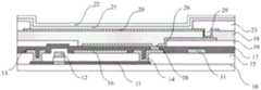
现有技术中的一种有机发光显示装置的基板结构如图1a和图1b所示,该有机发光显示装置的基板包括薄膜晶体管以及发光结构(有机发光二极管),薄膜晶体管与发光结构之间设有介质层30以及平坦化层24,发光结构的第一电极通过有介质层30以及平坦化层24中的通孔25与薄膜晶体管的漏极连接。由于平坦化层24的上表面在通孔25处不平整,因此在平坦化层24的通孔25处以及其附近不能设置发光区,也就说该有机发光显示装置的发光区为了避开平坦化层24的通孔25,只能覆盖部分膜晶体管(不能覆盖薄膜晶体管的漏极),这样限制有机发光显示装置的发光面积,从而降低有机发光显示装置的亮度。A substrate structure of an organic light-emitting display device in the prior art is shown in FIG. 1a and FIG. 1b. The substrate of the organic light-emitting display device includes a thin film transistor and a light-emitting structure (organic light-emitting diode). There is a
发明内容SUMMARY OF THE INVENTION
本发明至少部分解决现有的有机发光显示基板的发光面积小而亮度低的问题,提供一种发光面积大的有机发光显示基板及其制作方法。The present invention at least partially solves the problems of small light-emitting area and low brightness of the existing organic light-emitting display substrate, and provides an organic light-emitting display substrate with a large light-emitting area and a manufacturing method thereof.
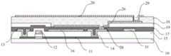
解决本发明技术问题所采用的技术方案是一种有机发光显示基板,包括衬底、设于所述衬底上的驱动晶体管以及设于所述驱动晶体管远离所述衬底一侧的有机发光二极管,其中所述有机发光二极管位于发光区中,所述发光区之外为非发光区,所述有机发光显示基板还包括:The technical solution adopted to solve the technical problem of the present invention is an organic light-emitting display substrate, comprising a substrate, a driving transistor disposed on the substrate, and an organic light-emitting diode disposed on the side of the driving transistor away from the substrate , wherein the organic light-emitting diode is located in the light-emitting area, the outside of the light-emitting area is a non-light-emitting area, and the organic light-emitting display substrate further includes:
覆盖所述驱动晶体管的源极和漏极的绝缘层;an insulating layer covering the source and drain of the drive transistor;
设于所述绝缘层远离所述衬底一侧的辅助导电结构,所述辅助导电结构通过所述绝缘层中的第一过孔与所述漏极连接;an auxiliary conductive structure disposed on the side of the insulating layer away from the substrate, the auxiliary conductive structure is connected to the drain through a first via hole in the insulating layer;
设于所述辅助导电结构远离所述衬底一侧的第一平坦化层,所述第一平坦化层包括第二过孔,所述有机发光二极管通过所述第二过孔与所述辅助导电结构连接;a first planarization layer disposed on the side of the auxiliary conductive structure away from the substrate, the first planarization layer includes a second via hole, and the organic light emitting diode communicates with the auxiliary via the second via hole Conductive structure connection;
所述驱动晶体管、所述第一过孔设于所述发光区,所述第二过孔设于所述非发光区,所述第一过孔与所述第二过孔之间设有与所述漏极同层设置的引线。The driving transistor and the first via hole are arranged in the light emitting region, the second via hole is arranged in the non-light emitting region, and a connection between the first via hole and the second via hole is arranged. The drain wire is arranged on the same layer as the lead.
进一步优选的是,该有机发光显示基板还包括:反光导电层,设于所述第一平坦化层远离所述衬底的一侧,位于所述发光区的所述反光导电层为所述有机发光二极管的第一电极,所述反光导电层通过所述第二过孔与所述辅助导电结构连接。Further preferably, the organic light-emitting display substrate further comprises: a light-reflecting conductive layer disposed on the side of the first planarization layer away from the substrate, and the light-reflecting conductive layer located in the light-emitting area is the organic light-emitting layer. The first electrode of the light emitting diode, the light-reflecting conductive layer is connected to the auxiliary conductive structure through the second via hole.
进一步优选的是,该有机发光显示基板还包括:与所述源极和所述漏极同层设置的电极层,所述电极层与所述驱动晶体管的栅极电连接,所述辅助导电结构的至少一部分与所述电极层对应,使得所述电极层与所述辅助导电结构形成第一电容。Further preferably, the organic light emitting display substrate further comprises: an electrode layer disposed in the same layer as the source electrode and the drain electrode, the electrode layer is electrically connected to the gate electrode of the driving transistor, and the auxiliary conductive structure At least a part of the electrode layer corresponds to the electrode layer, so that the electrode layer and the auxiliary conductive structure form a first capacitance.
进一步优选的是,所述驱动晶体管的有源层包括:非导体化区域以及导体化区域,所述非导体化区域与所述栅极对应,所述源极、所述漏极分别与所述导体化区域连接,所述导体化区域的至少一部分与所述电极层对应,形成第二电容。Further preferably, the active layer of the driving transistor includes: a non-conducting region and a conducting region, the non-conducting region corresponds to the gate, and the source and the drain are respectively connected to the The conductive region is connected, and at least a part of the conductive region corresponds to the electrode layer to form a second capacitor.
进一步优选的是,该有机发光显示基板还包括:第二平坦化层,位于所述辅助导电结构与所述绝缘层之间,且所述第二平坦至少位于所述第二过孔处。Further preferably, the organic light emitting display substrate further includes: a second planarization layer located between the auxiliary conductive structure and the insulating layer, and the second planarization layer is located at least at the second via hole.
进一步优选的是,所述驱动晶体管的栅极设置于所述驱动晶体管的有源层的远离所述衬底一侧,且所述栅极与所述驱动晶体管的有源层之间设有栅绝缘层。Further preferably, the gate of the driving transistor is arranged on the side of the active layer of the driving transistor away from the substrate, and a gate is arranged between the gate and the active layer of the driving transistor Insulation.
解决本发明技术问题所采用的技术方案是一种上述任意一种有机发光显示基板的制作方法,包括:The technical solution adopted to solve the technical problem of the present invention is a manufacturing method of any of the above organic light-emitting display substrates, including:
形成所述源极和所述漏极;forming the source and the drain;
形成所述绝缘层,在所述绝缘层中形成与所述漏极连接的所述第一过孔;forming the insulating layer, and forming the first via hole connected to the drain in the insulating layer;
形成所述辅助导电结构;forming the auxiliary conductive structure;
形成所述第一平坦化层,在所述第一平坦化层中形成与所述辅助导电结构连接的所述第二过孔;forming the first planarization layer, and forming the second via hole connected to the auxiliary conductive structure in the first planarization layer;
形成所述有机发光二极管。forming the organic light emitting diode.
进一步优选的是,所述有机发光显示基板为上述具反光导电层的有机发光显示基板,所述形成有机发光二极管包括:形成所述反光导电层;形成像素限定层;形成所述像素限定层的开口,所述开口对应所述发光区;形成有机发光层以及第二电极,所述有机发光层以及所述第二电极在所述开口处与所述反光导电层叠置。Further preferably, the organic light-emitting display substrate is the above-mentioned organic light-emitting display substrate with a light-reflecting conductive layer, and the forming an organic light-emitting diode includes: forming the light-reflecting conductive layer; forming a pixel-defining layer; forming the pixel-defining layer; an opening, the opening corresponds to the light-emitting region; an organic light-emitting layer and a second electrode are formed, and the organic light-emitting layer and the second electrode are stacked with the light-reflecting conductive layer at the opening.
进一步优选的是,所述有机发光显示基板为上述具有第二平坦化层的有机发光显示基板,在所述形成辅助导电结构之前包括:形成第二平坦化层。Further preferably, the organic light-emitting display substrate is the above-mentioned organic light-emitting display substrate with a second planarization layer, and before the forming of the auxiliary conductive structure includes: forming a second planarization layer.
解决本发明技术问题所采用的技术方案是一种有机发光显示装置,包括上述任意一个所述的有机发光显示基板。The technical solution adopted to solve the technical problem of the present invention is an organic light-emitting display device, which includes any one of the organic light-emitting display substrates described above.
附图说明Description of drawings
图1a为现有的一种有机发光显示装置的基板剖面结构图;1a is a cross-sectional structural diagram of a substrate of a conventional organic light-emitting display device;
图1b为现有的一种有机发光显示装置的基板俯视图;FIG. 1b is a top plan view of a substrate of a conventional organic light-emitting display device;
图2a为本发明的实施例的一种有机发光显示基板剖面结构图;2a is a cross-sectional structural diagram of an organic light-emitting display substrate according to an embodiment of the present invention;
图2b为本发明的实施例的一种有机发光显示基板俯视结构图;FIG. 2b is a top-view structural view of an organic light-emitting display substrate according to an embodiment of the present invention;
图3a至3d为本发明的实施例的一种有机发光显示基板制作方法各个步骤对应的剖面图;3a to 3d are cross-sectional views corresponding to various steps of a method for fabricating an organic light-emitting display substrate according to an embodiment of the present invention;
其中,附图标记为:10衬底;11有源层;12栅极;13源极;14漏极;15层间介质层;16电极层;17绝缘层;18第一平坦化层;19第二平坦化层;20反光导电层;21有机发光层;22第二电极;23像素限定层;24平坦化层;25通孔;26辅助导电结构;27发光区;28第一过孔;29第二过孔;30介质层;31引线。Wherein, the reference signs are: 10 substrate; 11 active layer; 12 gate; 13 source electrode; 14 drain electrode; 15 interlayer dielectric layer; 16 electrode layer; 17 insulating layer; 18 first planarization layer; 19 20 reflective conductive layer; 21 organic light emitting layer; 22 second electrode; 23 pixel defining layer; 24 planarization layer; 25 through hole; 26 auxiliary conductive structure; 27 light emitting area; 29 second via; 30 dielectric layer; 31 lead.
具体实施方式Detailed ways
为使本领域技术人员更好地理解本发明的技术方案,下面结合附图和具体实施方式对本发明作进一步详细描述。In order to make those skilled in the art better understand the technical solutions of the present invention, the present invention will be further described in detail below with reference to the accompanying drawings and specific embodiments.
在本发明中,两结构“同层设置”是指二者是由同一个材料层形成的,故它们在层叠关系上处于相同层中,但并不代表它们与衬底间的距离相等,也不代表它们与衬底间的其它层结构完全相同。In the present invention, the two structures are "disposed in the same layer" means that the two structures are formed of the same material layer, so they are in the same layer in the lamination relationship, but it does not mean that the distance between them and the substrate is equal, nor It does not mean that they are identical in structure to other layers between the substrates.
在本发明中,“构图工艺”是指形成具有特定的图形的结构的步骤,其可为光刻工艺,光刻工艺包括形成材料层、涂布光刻胶、曝光、显影、刻蚀、光刻胶剥离等步骤中的一步或多步;当然,“构图工艺”也可为压印工艺、喷墨打印工艺等其他工艺。In the present invention, "patterning process" refers to the step of forming a structure with a specific pattern, which can be a photolithography process, and the photolithography process includes forming a material layer, coating photoresist, exposing, developing, etching, photolithography One or more steps in steps such as resist stripping; of course, the "patterning process" can also be other processes such as imprinting, inkjet printing, and the like.
实施例1:Example 1:
如图2a和图2b所示,本实施例提供一种有机发光显示基板,包括衬底10、设于衬底10上的驱动晶体管以及设于驱动晶体管远离衬底10一侧的有机发光二极管,其中有机发光二极管位于发光区27中,发光区27之外为非发光区;有机发光显示基板还包括:As shown in FIG. 2a and FIG. 2b, the present embodiment provides an organic light emitting display substrate, which includes a
覆盖驱动晶体管的源极13和漏极14的绝缘层17;an
设于绝缘层17远离衬底10一侧的辅助导电结构26,辅助导电结构26通过绝缘层17中的第一过孔28与漏极14连接;The auxiliary
设于辅助导电结构26远离衬底10一侧的第一平坦化层18,第一平坦化层18包括第二过孔29,有机发光二极管通过第二过孔29与辅助导电结构26连接;The
驱动晶体管、第一过孔28设于发光区27,第二过孔29设于非发光区,第一过孔28与第二过孔29之间设有与漏极14同层设置的引线31。The driving transistor and the
其中,也就是说为了避开与漏极14同层设置的引线31(如数据线等)或者其他结构(如其他晶体管),通过设于驱动晶体管与有机发光二极管之间的辅助导电结构26实现驱动晶体管与有机发光二极管的电连接,具体的,辅助导电结构26通过设于其下的绝缘层17中的第一过孔28与驱动晶体管(如漏极14)连接,辅助导电结构26通过设于其上的第一平坦化层18中的第二过孔29与有机发光二极管(如第一电极)连接。由于第一平坦化层18中的第二过孔29可以设置在远离驱动晶体管以及第一过孔28的位置(该位置原本就是用于设置引线31等的非发光区,例如用于设置隔垫物的区域),这样可以使驱动晶体管、第一过孔28可位于有机发光二极管的发光区27,增大发光区27的面积占整个有机发光显示基板面积的比例,进而可以增强有机发光显示装置的亮度,改善该有机发光显示基板性能。Among them, that is to say, in order to avoid the leads 31 (such as data lines, etc.) or other structures (such as other transistors) provided in the same layer as the
优选的,本实施例的有机发光显示基板还包括:反光导电层20,设于第一平坦化层18远离衬底10的一侧,位于发光区27的反光导电层20为有机发光二极管的第一电极,反光导电层20通过第二过孔29与辅助导电结构26连接。Preferably, the organic light-emitting display substrate of this embodiment further includes: a light-reflecting
其中,也就是说反光导电层20设于第一平坦化层18的上表面以及第二过孔29处,位于发光区27的反光导电层20可以作为有机发光二极管的第一电极(如阳极),位于第二过孔29的反光导电层20与辅助导电结构26连接,从而实现有机发光二极管与辅助导电结构26的连接。That is to say, the light-reflecting
其中,反光导电层20具有反射性,故可将有机发光二极管发出的光反射向远离衬底10一侧,从而避免其影响驱动晶体管。也就是说本实施例提供的有机发光显示基板为“顶发射”式的有机发光显示基板。The light-reflecting
不作为第一电极的反光导电层20可用于连接第二过孔29与第一电极,从而允许第二过孔29的位置变化。因此,反光导电层20的设置不仅能够满足有机发光显示基板实现基本性能的基本要求,而且其可以与第二过孔29很好的配合,从而使得发光区27的面积增大。The light-reflecting
优选的,本实施例的有机发光显示基板还包括:与源极13和漏极14同层设置的电极层16,电极层16与驱动晶体管的栅极12电连接,辅助导电结构26的至少一部分与电极层16对应(即相对设置),使得电极层16与辅助导电结构26形成第一电容。Preferably, the organic light emitting display substrate of this embodiment further includes: an
其中,也就是说电极层16与位于发光区27的辅助导电结构26形成第一电容,第一电容可以是储存电容。That is to say, the
电极层16与栅极12电连接可以避免电极层16的浮接,保证电极层16与位于发光区27的辅助导电结构26形成的储存电容的有效性。The electrical connection between the
优选的,驱动晶体管的有源层11包括:非导体化区域以及导体化区域,非导体化区域与栅极12对应,源极13、漏极14分别与导体化区域连接,导体化区域的至少一部分与电极层16对应,形成第二电容。Preferably, the
其中,非导体化区域可以具有半导体的性能,即当在一定条件下才会导电。导体化区域可以具有导体的性能,即可以导电。非导体化区域和导体化区域之间是相互连接的,构成一个整体的有源层11。这里所说的第二电容是由电极层16和与其相对的导体化区域构成,从而最终的存储电容是由电极层16和与其相对的辅助导电结构26以及导体化区域构成的叠层电容。Among them, the non-conductive region can have the properties of a semiconductor, that is, it will conduct electricity only under certain conditions. The conductive region can have the properties of a conductor, that is, it can conduct electricity. The non-conductive region and the conductive region are connected to each other to form an integral
叠层电容不仅可以减少第二电容所占的空间,而且可以增大第二电容的容量,从而提高有机发光显示基板的性能。The stacked capacitor can not only reduce the space occupied by the second capacitor, but also increase the capacity of the second capacitor, thereby improving the performance of the organic light emitting display substrate.
优选的,本实施例的有机发光显示基板还包括:第二平坦化层19,位于辅助导电结构26与绝缘层17之间,且第二平坦化层19至少位于第二过孔29处。Preferably, the organic light emitting display substrate of this embodiment further includes: a
其中,也就是说第二平坦化层19设于绝缘层17的上表面,而辅助导电结构26位于非发光区的部分可以位于第二平坦化层19的上表面。此外,第二平坦化层19部分也可以位于发光区27内。Wherein, that is to say, the
第二平坦化层19可以提高辅助导电结构26与反光导电层20连接的位置,以使第一平坦化层18中的第二过孔29的深度减小,降低制作工艺的难度。此外,当第二平坦化层19部分也可以位于发光区27内时,由于在发光区27内有第一平坦化层18以及第二平坦化层19,可以进一步增强发光区27内层结构的平坦度,从而使得发光更加均匀。The
优选的,驱动晶体管的栅极12设置于驱动晶体管的有源层11的远离衬底10一侧,且栅极12与驱动晶体管的有源层11之间设有栅绝缘层。Preferably, the
其中,也就是说驱动晶体管为顶栅结构的晶体管。Among them, that is to say, the driving transistor is a transistor with a top-gate structure.
与底栅结构的晶体管相比,顶栅结构不仅可以减少有机发光显示基板的制作步骤,而且可以使得有机发光显示基板的整个厚度变薄。Compared with the transistor with the bottom gate structure, the top gate structure can not only reduce the fabrication steps of the organic light emitting display substrate, but also make the entire thickness of the organic light emitting display substrate thinner.
此外,本实施例还提供一种有机发光显示装置,其包括上述的有机发光显示基板,该有机发光显示装置具有亮度高等优点。In addition, this embodiment also provides an organic light-emitting display device, which includes the above-mentioned organic light-emitting display substrate, and the organic light-emitting display device has the advantages of high brightness.
实施例2:Example 2:
如图3a至3d和图2a所示,本实施例提供一种有机发光显示基板的制作方法,其包括:As shown in FIGS. 3 a to 3 d and FIG. 2 a , this embodiment provides a method for fabricating an organic light-emitting display substrate, which includes:
S10,如图3a所示,采用构图工艺在衬底10上形成驱动晶体管。S10 , as shown in FIG. 3 a , a patterning process is used to form a driving transistor on the
具体的,S11,根据预设的图案在衬底10的上表面形成有源层11,有源层11包括非导体化区域以及导体化区域。有源层11可以由有机半导体、氧化半导体等形成,例如可以包含a-IGZO、IZTO、a-Si、p-Si、六噻吩、聚噻吩等。而导体化区域是将半导体材料通过特殊工艺导体化而形成,以使得有源层11的导体化区域与电极层16形成电容。Specifically, in S11, an
S12,在有源层11的非导体化区域上形成栅绝缘层。栅绝缘层由绝缘材料构成,例如氧化物或者氮化物。S12 , a gate insulating layer is formed on the non-conductive region of the
S13,在栅绝缘层上表面形成栅极12。栅绝缘层将栅极12与有源层11间隔开。栅极12可以由高导电性材料构成,例如金属。本实施例的方法形成的驱动晶体管为顶栅结构。S13, forming the
S14,形成覆盖栅极12、栅绝缘层以及有源层11的层间介质层15,在形成层间介质层15中的过孔,使得有源层11的两个分离的区域的上表面暴露。层间介质层15包含但不限于聚硅氧烷系材料,亚克力系材料,或聚酰亚胺系材料等具有平坦化效果的材料。S14 , forming an
S15,形成源极13、漏极14以及电极层16(还包括引线31)。具体的,在层间介质层15的上表面以及过孔中形成导电层,使得导电层覆盖层间介质层15的上表面、第一过孔28的底面以及第一过孔28的侧面;再根据预设的图案除去源极13、漏极14、电极层16以及引线31之外的部分,以形成源极13、漏极14、电极层16以及引线31。S15, forming the
S20,如图3b所示,形成绝缘层17以及第二平坦化层19。S20, as shown in FIG. 3b, the insulating
具体的,S21,在源极13、漏极14、电极层16以及引线31上形成绝缘层17,绝缘层17将源极13、漏极14、电极层16以及引线31互相间隔,且覆盖源极13、漏极14、电极层16以及引线31。再根据预设的图案形成绝缘层17中的第一过孔28,第一过孔28与漏极14连接。绝缘层17由绝缘材料构成,例如氧化物或者氮化物等。Specifically, S21, an insulating
具体的,S22,在绝缘层17上形成平坦化材料层,根据预设的图案,在平坦化材料层中形成开口,形成第二平坦化层19,优选的,第二平坦化层19未覆盖绝缘层17的第一过孔28。Specifically, S22, a planarization material layer is formed on the insulating
S30,如图3c所示,形成辅助导电结构26。S30, as shown in FIG. 3c, the auxiliary
具体的,在绝缘层17以及第二平坦化层19上形成辅助导电结构26,使得辅助导电结构26通过绝缘层17的第一过孔28与漏极14连接。部分辅助导电结构26位于绝缘层17的上表面,且与电极层16相对;另一部分辅助导电结构26位于第二平坦化层19的上表面。Specifically, the auxiliary
S40,如图3d所示,形成第一平坦化层18以及反光导电层20。S40 , as shown in FIG. 3d , the
具体的,S41,在辅助导电结构26上以及其他结构暴露的上表面形成第一平坦化层18,使得第一平坦化层18覆盖包括辅助导电结构26的所有暴露的结构层。再根据预设的图案,在第一平坦化材料层中形成第二过孔29。第二过孔29与第二平坦化层19的上表面的辅助导电结构26连接。Specifically, S41 , the
S42,在第一平坦化层18上表面以及第二过孔29处形成反光导电层20,使得反光导电层20通过第二过孔29与辅助导电结构26连接。S42 , forming the light-reflecting
S50,如图2a所示,形成有机发光二极管。S50, as shown in FIG. 2a, an organic light emitting diode is formed.
具体的,S51,在第一平坦化层18以及反光导电层20上表面形成像素限定层23,并根据预设的图案去除与发光区27对应的像素限定层23,使得发光区27的反光导电层20暴露,形成第一电极(如阳极)。像素限定层23用于间隔有机发光显示基板的相邻子像素的发光区27。Specifically, in S51, the
S52,在第一电极以及部分素限定层上形成有机发光层21。S52, the organic light-emitting
S53,在有机发光层21的上表面的形成第二电极22(如阴极),使得有机发光层21将第一电极以及第二电极22间隔,以形成有机发光二极管。S53 , forming a second electrode 22 (eg, a cathode) on the upper surface of the organic
此外,本发明中的栅极12、源极13、漏极14、辅助导电结构26、第一电极以及第二电极22可以是常用的金属材料,如Ag、Cu、Al、Mo等,或多层金属如MoNb/Cu/MoNb等,或上述金属的合金材料,如AlNd、MoNb等,也可以是金属和透明导电氧化物(如ITO、AZO等)形成的堆栈结构,如ITO/Ag/ITO等。本发明中的层间介质层15、绝缘层17的材料包括但不限于常规的如SiOx、SiNx、SiON等介质材料,或各种新型的有机绝缘材料,或高介电常数(High k)材料如AlOx、HfOx、TaOx等。In addition, the
本发明中的反光导电层20由既可导电又可反光的材料构成,例如由可作为有机发光二极管的阳极的透明导电材料与金属材料堆栈构成。由此,本实施例的方法制作的有机发光显示基板为“顶发射”的形式,即光直接从有机发光二极管远离衬底10一侧射出,并不经过衬底10。The light-reflecting
本实施例的有机发光显示基板的制作方法,通过辅助导电结构26将与有机发光二极管连接的第二过孔29设于远离与驱动晶体管连接的第一过孔28,可以使发光区27覆盖驱动晶体管以及第一过孔28。这样可以增大有机发光显示基板的发光区27的面积,即可以增大发光区27的面积占整个有机发光显示基板面积的比例,从而可以增强有机发光显示装置的亮度,改善该有机发光显示基板性能。In the manufacturing method of the organic light emitting display substrate of this embodiment, the second via
可以理解的是,以上实施方式仅仅是为了说明本发明的原理而采用的示例性实施方式,然而本发明并不局限于此。对于本领域内的普通技术人员而言,在不脱离本发明的精神和实质的情况下,可以做出各种变型和改进,这些变型和改进也视为本发明的保护范围。It can be understood that the above embodiments are only exemplary embodiments adopted to illustrate the principle of the present invention, but the present invention is not limited thereto. For those skilled in the art, without departing from the spirit and essence of the present invention, various modifications and improvements can be made, and these modifications and improvements are also regarded as the protection scope of the present invention.
Claims (8)
Priority Applications (2)
| Application Number | Priority Date | Filing Date | Title |
|---|---|---|---|
| CN201810902568.0ACN109065590B (en) | 2018-08-09 | 2018-08-09 | Organic light-emitting display substrate and method of making the same, and organic light-emitting display device |
| US16/536,942US11043545B2 (en) | 2018-08-09 | 2019-08-09 | Display substrate, fabricating method thereof, and display device |
Applications Claiming Priority (1)
| Application Number | Priority Date | Filing Date | Title |
|---|---|---|---|
| CN201810902568.0ACN109065590B (en) | 2018-08-09 | 2018-08-09 | Organic light-emitting display substrate and method of making the same, and organic light-emitting display device |
Publications (2)
| Publication Number | Publication Date |
|---|---|
| CN109065590A CN109065590A (en) | 2018-12-21 |
| CN109065590Btrue CN109065590B (en) | 2020-12-04 |
Family
ID=64678916
Family Applications (1)
| Application Number | Title | Priority Date | Filing Date |
|---|---|---|---|
| CN201810902568.0AActiveCN109065590B (en) | 2018-08-09 | 2018-08-09 | Organic light-emitting display substrate and method of making the same, and organic light-emitting display device |
Country Status (2)
| Country | Link |
|---|---|
| US (1) | US11043545B2 (en) |
| CN (1) | CN109065590B (en) |
Families Citing this family (7)
| Publication number | Priority date | Publication date | Assignee | Title |
|---|---|---|---|---|
| CN110610975B (en)* | 2019-09-23 | 2022-04-08 | 京东方科技集团股份有限公司 | Display substrate, preparation method thereof and display device |
| KR102826842B1 (en)* | 2020-02-12 | 2025-06-30 | 삼성디스플레이 주식회사 | Display device and method of fabricating the same |
| TWI755034B (en)* | 2020-08-19 | 2022-02-11 | 友達光電股份有限公司 | Device substrate and manufacturing method thereof |
| US11997898B2 (en) | 2020-12-28 | 2024-05-28 | Boe Technology Group Co., Ltd. | Display panel and display device including blocker |
| CN113871399A (en)* | 2021-09-22 | 2021-12-31 | 合肥维信诺科技有限公司 | An array substrate and its manufacturing method, and a display panel |
| CN114464757B (en)* | 2022-02-09 | 2024-03-26 | 武汉天马微电子有限公司 | A display panel and display device |
| CN115172468B (en)* | 2022-07-11 | 2025-04-25 | 京东方科技集团股份有限公司 | Display substrate and manufacturing method thereof, and display device |
Citations (5)
| Publication number | Priority date | Publication date | Assignee | Title |
|---|---|---|---|---|
| CN101859793A (en)* | 2009-02-09 | 2010-10-13 | 三星移动显示器株式会社 | Organic light emitting diode display and manufacturing method thereof |
| CN103681745A (en)* | 2012-09-17 | 2014-03-26 | 三星显示有限公司 | Organic electroluminescent display and method of manufacturing the same |
| CN104022126A (en)* | 2014-05-28 | 2014-09-03 | 京东方科技集团股份有限公司 | Array substrate and manufacturing method thereof, and display apparatus |
| CN105408813A (en)* | 2013-08-26 | 2016-03-16 | 苹果公司 | Displays with silicon thin film transistors and semiconductor oxide thin film transistors |
| CN108242462A (en)* | 2018-01-12 | 2018-07-03 | 京东方科技集团股份有限公司 | Organic light-emitting display panel, manufacturing method thereof, and display device |
Family Cites Families (9)
| Publication number | Priority date | Publication date | Assignee | Title |
|---|---|---|---|---|
| US7161184B2 (en)* | 2003-06-16 | 2007-01-09 | Semiconductor Energy Laboratory Co., Ltd. | Display device and method for manufacturing the same |
| CN1822383A (en)* | 2006-01-09 | 2006-08-23 | 友达光电股份有限公司 | Organic electroluminescent display device |
| US9362345B2 (en)* | 2013-05-31 | 2016-06-07 | Samsung Display Co., Ltd. | Organic light emitting display apparatus and method of manufacturing the same |
| KR102180037B1 (en) | 2013-11-06 | 2020-11-18 | 삼성디스플레이 주식회사 | Flexible display and manufacturing method thereof |
| CN103745985B (en)* | 2013-12-27 | 2015-03-18 | 京东方科技集团股份有限公司 | Active matrix OLED (Organic Light-Emitting Diode) display substrate and display device |
| CN105097842A (en)* | 2015-08-11 | 2015-11-25 | 京东方科技集团股份有限公司 | Active matrix organic light emitting diode array substrate, manufacturing method and display device |
| KR102448611B1 (en)* | 2015-10-30 | 2022-09-27 | 엘지디스플레이 주식회사 | organic light emitting diode display |
| KR102718848B1 (en)* | 2016-08-12 | 2024-10-18 | 삼성디스플레이 주식회사 | Display device |
| KR20180071538A (en)* | 2016-12-20 | 2018-06-28 | 엘지디스플레이 주식회사 | Substrate for display and display including the same |
- 2018
- 2018-08-09CNCN201810902568.0Apatent/CN109065590B/enactiveActive
- 2019
- 2019-08-09USUS16/536,942patent/US11043545B2/enactiveActive
Patent Citations (5)
| Publication number | Priority date | Publication date | Assignee | Title |
|---|---|---|---|---|
| CN101859793A (en)* | 2009-02-09 | 2010-10-13 | 三星移动显示器株式会社 | Organic light emitting diode display and manufacturing method thereof |
| CN103681745A (en)* | 2012-09-17 | 2014-03-26 | 三星显示有限公司 | Organic electroluminescent display and method of manufacturing the same |
| CN105408813A (en)* | 2013-08-26 | 2016-03-16 | 苹果公司 | Displays with silicon thin film transistors and semiconductor oxide thin film transistors |
| CN104022126A (en)* | 2014-05-28 | 2014-09-03 | 京东方科技集团股份有限公司 | Array substrate and manufacturing method thereof, and display apparatus |
| CN108242462A (en)* | 2018-01-12 | 2018-07-03 | 京东方科技集团股份有限公司 | Organic light-emitting display panel, manufacturing method thereof, and display device |
Also Published As
| Publication number | Publication date |
|---|---|
| US20200052053A1 (en) | 2020-02-13 |
| US11043545B2 (en) | 2021-06-22 |
| CN109065590A (en) | 2018-12-21 |
Similar Documents
| Publication | Publication Date | Title |
|---|---|---|
| CN109065590B (en) | Organic light-emitting display substrate and method of making the same, and organic light-emitting display device | |
| CN109728000B (en) | Transparent display substrate and display panel | |
| JP7486523B2 (en) | Display substrate and its manufacturing method, display device | |
| TWI671898B (en) | Organic light-emitting diode display | |
| CN109037297B (en) | Organic light-emitting display substrate and manufacturing method thereof | |
| CN108735792B (en) | Bottom emission type OLED array substrate and manufacturing method thereof, display panel and display device | |
| CN112703605B (en) | Display device, manufacturing method thereof, and drive substrate | |
| KR101073552B1 (en) | Organic light emitting diode display and method of manufacturing the same | |
| CN101728374B (en) | Dual panel type organic electroluminescent display device and method of fabricating the same | |
| CN112103326A (en) | Display panel, manufacturing method thereof and display device | |
| CN101752400B (en) | Image display device, image display system and manufacturing method thereof | |
| EP2744008A1 (en) | Array substrate, method for fabricating the same, and OLED display device | |
| CN106997893B (en) | Organic light emitting display device and method of manufacturing the same | |
| CN105470279A (en) | Organic light emitting display device and method of manufacturing same | |
| CN105552249A (en) | OLED display substrate, manufacturing method thereof and display device | |
| CN112259579B (en) | OLED display panel and manufacturing method thereof | |
| JP4637831B2 (en) | ORGANIC ELECTROLUMINESCENCE ELEMENT, ITS MANUFACTURING METHOD, AND DISPLAY DEVICE | |
| CN113812014B (en) | Array substrate, preparation method thereof and display panel | |
| JP6223070B2 (en) | Organic EL display device and method of manufacturing organic EL display device | |
| CN109427820A (en) | A kind of substrate and preparation method thereof, display panel | |
| CN109935580A (en) | Substrate, manufacturing method thereof and electronic device | |
| CN112103398B (en) | A display panel | |
| CN212934665U (en) | a display panel | |
| CN113078269B (en) | Organic electroluminescence structure, method for making the same, and display device | |
| CN113078270A (en) | Organic electroluminescent structure, manufacturing method thereof and display device |
Legal Events
| Date | Code | Title | Description |
|---|---|---|---|
| PB01 | Publication | ||
| PB01 | Publication | ||
| SE01 | Entry into force of request for substantive examination | ||
| SE01 | Entry into force of request for substantive examination | ||
| GR01 | Patent grant | ||
| GR01 | Patent grant |