CN109031839B - A panel, driving method, preparation method, regulating device and regulating system - Google Patents
A panel, driving method, preparation method, regulating device and regulating systemDownload PDFInfo
- Publication number
- CN109031839B CN109031839BCN201811024606.3ACN201811024606ACN109031839BCN 109031839 BCN109031839 BCN 109031839BCN 201811024606 ACN201811024606 ACN 201811024606ACN 109031839 BCN109031839 BCN 109031839B
- Authority
- CN
- China
- Prior art keywords
- electrode layer
- layer
- flexible electrode
- voltage
- groove structure
- Prior art date
- Legal status (The legal status is an assumption and is not a legal conclusion. Google has not performed a legal analysis and makes no representation as to the accuracy of the status listed.)
- Active
Links
Images


Classifications
- G—PHYSICS
- G02—OPTICS
- G02F—OPTICAL DEVICES OR ARRANGEMENTS FOR THE CONTROL OF LIGHT BY MODIFICATION OF THE OPTICAL PROPERTIES OF THE MEDIA OF THE ELEMENTS INVOLVED THEREIN; NON-LINEAR OPTICS; FREQUENCY-CHANGING OF LIGHT; OPTICAL LOGIC ELEMENTS; OPTICAL ANALOGUE/DIGITAL CONVERTERS
- G02F1/00—Devices or arrangements for the control of the intensity, colour, phase, polarisation or direction of light arriving from an independent light source, e.g. switching, gating or modulating; Non-linear optics
- G02F1/01—Devices or arrangements for the control of the intensity, colour, phase, polarisation or direction of light arriving from an independent light source, e.g. switching, gating or modulating; Non-linear optics for the control of the intensity, phase, polarisation or colour
- G02F1/15—Devices or arrangements for the control of the intensity, colour, phase, polarisation or direction of light arriving from an independent light source, e.g. switching, gating or modulating; Non-linear optics for the control of the intensity, phase, polarisation or colour based on an electrochromic effect
- G02F1/153—Constructional details
- G02F1/155—Electrodes
- G—PHYSICS
- G02—OPTICS
- G02B—OPTICAL ELEMENTS, SYSTEMS OR APPARATUS
- G02B26/00—Optical devices or arrangements for the control of light using movable or deformable optical elements
- G02B26/02—Optical devices or arrangements for the control of light using movable or deformable optical elements for controlling the intensity of light
- G02B26/023—Optical devices or arrangements for the control of light using movable or deformable optical elements for controlling the intensity of light comprising movable attenuating elements, e.g. neutral density filters
- E—FIXED CONSTRUCTIONS
- E06—DOORS, WINDOWS, SHUTTERS, OR ROLLER BLINDS IN GENERAL; LADDERS
- E06B—FIXED OR MOVABLE CLOSURES FOR OPENINGS IN BUILDINGS, VEHICLES, FENCES OR LIKE ENCLOSURES IN GENERAL, e.g. DOORS, WINDOWS, BLINDS, GATES
- E06B9/00—Screening or protective devices for wall or similar openings, with or without operating or securing mechanisms; Closures of similar construction
- E06B9/24—Screens or other constructions affording protection against light, especially against sunshine; Similar screens for privacy or appearance; Slat blinds
- G—PHYSICS
- G02—OPTICS
- G02F—OPTICAL DEVICES OR ARRANGEMENTS FOR THE CONTROL OF LIGHT BY MODIFICATION OF THE OPTICAL PROPERTIES OF THE MEDIA OF THE ELEMENTS INVOLVED THEREIN; NON-LINEAR OPTICS; FREQUENCY-CHANGING OF LIGHT; OPTICAL LOGIC ELEMENTS; OPTICAL ANALOGUE/DIGITAL CONVERTERS
- G02F1/00—Devices or arrangements for the control of the intensity, colour, phase, polarisation or direction of light arriving from an independent light source, e.g. switching, gating or modulating; Non-linear optics
- G02F1/01—Devices or arrangements for the control of the intensity, colour, phase, polarisation or direction of light arriving from an independent light source, e.g. switching, gating or modulating; Non-linear optics for the control of the intensity, phase, polarisation or colour
- G02F1/15—Devices or arrangements for the control of the intensity, colour, phase, polarisation or direction of light arriving from an independent light source, e.g. switching, gating or modulating; Non-linear optics for the control of the intensity, phase, polarisation or colour based on an electrochromic effect
- G02F1/153—Constructional details
- G—PHYSICS
- G02—OPTICS
- G02F—OPTICAL DEVICES OR ARRANGEMENTS FOR THE CONTROL OF LIGHT BY MODIFICATION OF THE OPTICAL PROPERTIES OF THE MEDIA OF THE ELEMENTS INVOLVED THEREIN; NON-LINEAR OPTICS; FREQUENCY-CHANGING OF LIGHT; OPTICAL LOGIC ELEMENTS; OPTICAL ANALOGUE/DIGITAL CONVERTERS
- G02F1/00—Devices or arrangements for the control of the intensity, colour, phase, polarisation or direction of light arriving from an independent light source, e.g. switching, gating or modulating; Non-linear optics
- G02F1/01—Devices or arrangements for the control of the intensity, colour, phase, polarisation or direction of light arriving from an independent light source, e.g. switching, gating or modulating; Non-linear optics for the control of the intensity, phase, polarisation or colour
- G02F1/15—Devices or arrangements for the control of the intensity, colour, phase, polarisation or direction of light arriving from an independent light source, e.g. switching, gating or modulating; Non-linear optics for the control of the intensity, phase, polarisation or colour based on an electrochromic effect
- G02F1/163—Operation of electrochromic cells, e.g. electrodeposition cells; Circuit arrangements therefor
- E—FIXED CONSTRUCTIONS
- E06—DOORS, WINDOWS, SHUTTERS, OR ROLLER BLINDS IN GENERAL; LADDERS
- E06B—FIXED OR MOVABLE CLOSURES FOR OPENINGS IN BUILDINGS, VEHICLES, FENCES OR LIKE ENCLOSURES IN GENERAL, e.g. DOORS, WINDOWS, BLINDS, GATES
- E06B9/00—Screening or protective devices for wall or similar openings, with or without operating or securing mechanisms; Closures of similar construction
- E06B9/24—Screens or other constructions affording protection against light, especially against sunshine; Similar screens for privacy or appearance; Slat blinds
- E06B2009/2417—Light path control; means to control reflection
- E—FIXED CONSTRUCTIONS
- E06—DOORS, WINDOWS, SHUTTERS, OR ROLLER BLINDS IN GENERAL; LADDERS
- E06B—FIXED OR MOVABLE CLOSURES FOR OPENINGS IN BUILDINGS, VEHICLES, FENCES OR LIKE ENCLOSURES IN GENERAL, e.g. DOORS, WINDOWS, BLINDS, GATES
- E06B9/00—Screening or protective devices for wall or similar openings, with or without operating or securing mechanisms; Closures of similar construction
- E06B9/24—Screens or other constructions affording protection against light, especially against sunshine; Similar screens for privacy or appearance; Slat blinds
- E06B2009/2464—Screens or other constructions affording protection against light, especially against sunshine; Similar screens for privacy or appearance; Slat blinds featuring transparency control by applying voltage, e.g. LCD, electrochromic panels
Landscapes
- Physics & Mathematics (AREA)
- Nonlinear Science (AREA)
- General Physics & Mathematics (AREA)
- Optics & Photonics (AREA)
- Engineering & Computer Science (AREA)
- Structural Engineering (AREA)
- Architecture (AREA)
- Civil Engineering (AREA)
- Electrochromic Elements, Electrophoresis, Or Variable Reflection Or Absorption Elements (AREA)
Abstract
Translated fromChinese
Description
Translated fromChinese技术领域technical field
本发明涉及电控调光相关技术领域,特别是指一种面板、驱动方法、制备方法、调控装置及调控系统。The present invention relates to the technical field of electronically controlled dimming, in particular to a panel, a driving method, a preparation method, a control device and a control system.
背景技术Background technique
智能电控调光玻璃于2003年开始进入国内市场。由于售价昂贵且识者甚少,往后的近十年间在中国发展缓慢。近年来,随着国民经济的持续高速增长,国内建材市场发展迅猛,智能电控调光玻璃渐渐为建筑及设计业界所接受并开始应用,主要应用于建筑和交通领域。智能玻璃所用技术主要有液晶、电致变色、光致变色、热致变色等,其中电致变色在飞机车窗上已有使用。Smart electronically controlled dimming glass began to enter the domestic market in 2003. Due to the high price and few knowledgeable people, it developed slowly in China in the next ten years. In recent years, with the sustained and rapid growth of the national economy, the domestic building materials market has developed rapidly. The technologies used in smart glass mainly include liquid crystal, electrochromic, photochromic, thermochromic, etc. Among them, electrochromic has been used in aircraft windows.
但是当前调光玻璃的卷曲设计使得在绝缘电介质层203上形成有凸起,而这可能由于不经意的外部摩擦或其它受力导致卷曲部分受损或遮挡,从而导致严重不良。However, the curly design of the current switchable glass causes protrusions to be formed on the insulating
发明内容SUMMARY OF THE INVENTION
有鉴于此,本发明的目的在于提出一种面板、驱动方法、制备方法、调控装置及调控系统,能够有效避免电控调光设备基于卷曲部分的凸起引起的受损或遮挡,保证调控的准确有效。In view of this, the purpose of the present invention is to provide a panel, a driving method, a preparation method, a control device and a control system, which can effectively avoid the damage or occlusion caused by the protrusion of the curled part of the electronically controlled dimming device, and ensure the controllability. Accurate and effective.
基于上述目的,第一方面,本发明实施例提供的面板包括基板、依次设置于所述基板上的第一透明电极层和绝缘层,以及设置于所述绝缘层上的卷曲结构;所述卷曲结构包括第二柔性电极层且所述卷曲结构预设有卷曲的固有应力;所述卷曲结构用于在伸展时吸收或者反射光线;Based on the above purpose, in a first aspect, a panel provided by an embodiment of the present invention includes a substrate, a first transparent electrode layer and an insulating layer arranged on the substrate in sequence, and a curling structure arranged on the insulating layer; the curling The structure includes a second flexible electrode layer and the crimped structure is preset with an inherent stress of the crimp; the crimped structure is used for absorbing or reflecting light when stretched;
所述第一透明电极层和所述绝缘层对应同一位置形成有凹槽结构;所述卷曲结构设置于所述凹槽结构内。A groove structure is formed on the first transparent electrode layer and the insulating layer corresponding to the same position; the curling structure is arranged in the groove structure.
在一些可选的实施方式中,所述基板上形成有定位槽,所述第一透明电极层和所述绝缘层在所述定位槽上形成有凹槽结构。In some optional embodiments, a positioning groove is formed on the substrate, and a groove structure is formed on the positioning groove for the first transparent electrode layer and the insulating layer.
在一些可选的实施方式中,所述基板上设置有基质层,所述基质层上形成有定位槽,所述第一透明电极层和所述绝缘层依次设置于所述基质层上且所述第一透明电极层和所述绝缘层在所述定位槽上形成有凹槽结构。In some optional embodiments, a matrix layer is provided on the substrate, a positioning groove is formed on the matrix layer, the first transparent electrode layer and the insulating layer are sequentially arranged on the matrix layer, and the A groove structure is formed on the positioning groove on the first transparent electrode layer and the insulating layer.
在一些可选的实施方式中,所述凹槽结构呈倒梯型且所述凹槽结构的深度大于或等于所述第二柔性电极层卷曲后形成的卷曲高度。In some optional embodiments, the groove structure is an inverted trapezoid, and the depth of the groove structure is greater than or equal to a curling height formed after the second flexible electrode layer is curled.
在一些可选的实施方式中,所述凹槽结构内设置有第一触点电极;所述第二柔性电极层的一端通过所述第一触点电极与所述绝缘层固定连接;所述第一触点电极用于给所述第二柔性电极层供电。In some optional embodiments, a first contact electrode is disposed in the groove structure; one end of the second flexible electrode layer is fixedly connected to the insulating layer through the first contact electrode; the The first contact electrode is used to supply power to the second flexible electrode layer.
在一些可选的实施方式中,所述第一透明电极层靠近所述凹槽结构的一端设置有第二触点电极;所述第二触点电极用于给所述第一透明电极层供电。In some optional embodiments, a second contact electrode is provided at one end of the first transparent electrode layer close to the groove structure; the second contact electrode is used to supply power to the first transparent electrode layer .
在一些可选的实施方式中,所述绝缘层远离所述凹槽结构的一端设置有第三触点电极;所述第三触点电极用于作为所述第二柔性电极层展开时的定位结构。In some optional embodiments, a third contact electrode is provided at one end of the insulating layer away from the groove structure; the third contact electrode is used for positioning when the second flexible electrode layer is unfolded structure.
在一些可选的实施方式中,所述第三触点电极对应所述凹槽结构的一侧设置有斜面结构。In some optional implementation manners, a slope structure is provided on a side of the third contact electrode corresponding to the groove structure.
在一些可选的实施方式中,所述第二柔性电极层对应所述第三触点电极的一端设置有与所述第三触点电极配合的端头结构。In some optional implementations, an end of the second flexible electrode layer corresponding to the third contact electrode is provided with a terminal structure matched with the third contact electrode.
在一些可选的实施方式中,所述卷曲结构还包括聚合物层;所述第二柔性电极层与所述聚合物层贴合设置,且所述第二柔性电极层与所述聚合物层中的至少一层预设有卷曲的固有应力。In some optional embodiments, the crimped structure further includes a polymer layer; the second flexible electrode layer and the polymer layer are disposed in contact, and the second flexible electrode layer and the polymer layer At least one of the layers is pre-set with the inherent stress of curling.
在一些可选的实施方式中,所述聚合物层设置于所述第二柔性电极层远离所述第一透明电极层的一侧。In some optional embodiments, the polymer layer is disposed on a side of the second flexible electrode layer away from the first transparent electrode layer.
在一些可选的实施方式中,所述第一透明电极层包括多个间隔排布的条状电极,所述多个条状电极的排布方向与所述第二柔性电极层的伸展方向相同。In some optional embodiments, the first transparent electrode layer includes a plurality of strip-shaped electrodes arranged at intervals, and the arrangement direction of the plurality of strip-shaped electrodes is the same as the extending direction of the second flexible electrode layer .
第二方面,本申请实施例还提供了一种调控装置,所述调控装置包括上述任一项所述的面板。In a second aspect, an embodiment of the present application further provides a control device, where the control device includes the panel described in any one of the above.
第三方面,本申请实施例还提供了一种调控系统,所述调控系统包括上述任一项所述的面板或所述调控装置;进一步还包括用于供电的电源以及用于控制所述第二柔性电极层伸展或者卷曲的控制单元。In a third aspect, an embodiment of the present application further provides a control system, the control system includes the panel or the control device described in any one of the above; further includes a power supply for power supply and a control system for controlling the first Two flexible electrode layers stretch or curl the control unit.
第四方面,本申请实施例还提供了一种上述任一项所述面板的驱动方法,所述驱动方法包括伸展驱动和卷曲驱动;In a fourth aspect, an embodiment of the present application further provides a method for driving the panel according to any one of the above, wherein the driving method includes stretching driving and curling driving;
所述伸展驱动包括:The stretch drive includes:
在所述第二柔性电极层位于所述凹槽结构内的第一阶段,向所述第一透明电极层输入预设的基准电压,向所述第二柔性电极层输入预设的爬坡电压,所述爬坡电压用于驱动所述第二柔性电极层从所述凹槽结构内伸展出去;In the first stage when the second flexible electrode layer is located in the groove structure, a preset reference voltage is input to the first transparent electrode layer, and a preset ramp voltage is input to the second flexible electrode layer , the ramping voltage is used to drive the second flexible electrode layer to stretch out from the groove structure;
在所述第二柔性电极层至少部分离开所述凹槽结构内的第二阶段,向所述第二柔性电极层输入预设的舒展电压,所述舒展电压用于驱动所述第二柔性电极层沿紧靠所述第一透明电极层的方向伸展;其中,所述舒展电压小于所述爬坡电压;In the second stage when the second flexible electrode layer at least partially leaves the groove structure, a preset stretching voltage is input to the second flexible electrode layer, and the stretching voltage is used to drive the second flexible electrode the layer stretches in a direction close to the first transparent electrode layer; wherein the stretch voltage is less than the ramp voltage;
或者,or,
在所述第二柔性电极层位于所述凹槽结构内的第一阶段,向所述第二柔性电极层输入预设的基准电压,向所述第一透明电极层输入预设的爬坡电压,所述爬坡电压用于驱动所述第二柔性电极层从所述凹槽结构内伸展出去;In the first stage when the second flexible electrode layer is located in the groove structure, a preset reference voltage is input to the second flexible electrode layer, and a preset ramp voltage is input to the first transparent electrode layer , the ramping voltage is used to drive the second flexible electrode layer to stretch out from the groove structure;
在所述第二柔性电极层至少部分离开所述凹槽结构内的第二阶段,向所述第一透明电极层输入预设的舒展电压,所述舒展电压用于驱动所述第二柔性电极层沿紧靠所述第一透明电极层的方向伸展;其中,所述舒展电压小于所述爬坡电压;In the second stage when the second flexible electrode layer at least partially leaves the groove structure, a preset stretching voltage is input to the first transparent electrode layer, and the stretching voltage is used to drive the second flexible electrode the layer stretches in a direction close to the first transparent electrode layer; wherein the stretch voltage is less than the ramp voltage;
所述卷曲驱动包括:The curling drive includes:
撤销所述第一透明电极层或所述第二柔性电极层中的至少一个的电压,用于使得所述第二柔性电极层在固有应力的作用下回卷到所述凹槽结构内。Removing the voltage of at least one of the first transparent electrode layer or the second flexible electrode layer is used to cause the second flexible electrode layer to roll back into the groove structure under the action of inherent stress.
在一些可选的实施方式中,还包括:In some optional embodiments, it also includes:
在所述第二柔性电极层完全伸展的第三阶段,向所述第二柔性电极层或者所述第一透明电极层输入预设的维持电压,所述维持电压用于驱动所述第二柔性电极层抵抗固有应力以维持伸展状态;其中,所述维持电压小于所述舒展电压。In the third stage when the second flexible electrode layer is fully extended, a preset sustaining voltage is input to the second flexible electrode layer or the first transparent electrode layer, and the sustaining voltage is used to drive the second flexible electrode layer. The electrode layer resists intrinsic stress to maintain a stretched state; wherein the sustaining voltage is less than the stretching voltage.
第五方面,本申请实施例还提供了一种所述面板的驱动方法,驱动方法包括:向所述第一透明电极层输入控制电压时根据所述第二柔性电极层的伸展位置向对应的条状电极输入控制电压或者改变对应的条状电极输入控制电压的大小;In a fifth aspect, an embodiment of the present application further provides a driving method of the panel, the driving method comprising: when inputting a control voltage to the first transparent electrode layer, according to the stretched position of the second flexible electrode layer to a corresponding The strip electrode input control voltage or change the size of the corresponding strip electrode input control voltage;
其中,多个间隔排布的条状电极为单独驱动电极;所述控制电压与所述第二柔性电极层中施加的电压对应形成抵抗所述第二柔性电极层固有应力的反作用力。The plurality of strip electrodes arranged at intervals are independent drive electrodes; the control voltage corresponds to the voltage applied in the second flexible electrode layer to form a reaction force against the inherent stress of the second flexible electrode layer.
第六方面,本申请实施例还提供了一种上述任一项所述面板的制备方法,所述制备方法包括:In a sixth aspect, an embodiment of the present application further provides a method for manufacturing the panel described above, the manufacturing method comprising:
在所述基板上依次形成第一透明电极层和绝缘层且使得所述第一透明电极层和绝缘层对应形成有凹槽结构;forming a first transparent electrode layer and an insulating layer on the substrate in sequence, so that the first transparent electrode layer and the insulating layer are correspondingly formed with a groove structure;
将包含有第二柔性电极层的卷曲结构设置在所述凹槽结构中;其中,所述卷曲结构预设有卷曲的固有应力。The crimp structure including the second flexible electrode layer is arranged in the groove structure; wherein, the crimp structure is preset with the inherent stress of the crimp.
从上面所述可以看出,本发明实施例提供的面板、驱动方法、制备方法、调控装置及调控系统,通过在下层的基板或者绝缘层上设置合适的凹槽结构,从而使得卷曲部分的结构能够与基板之间实现相对找平,进而避免受到制作过程或制作以后的外部摩擦或其它受力影响,导致卷曲部分的遮挡或损坏。因此,本申请上述面板能够有效避免基于卷曲部分的凸起引起的受损或遮挡,保证调控的准确有效。It can be seen from the above that the panel, the driving method, the manufacturing method, the control device and the control system provided by the embodiments of the present invention can make the structure of the curled part by setting a suitable groove structure on the lower substrate or the insulating layer. It can achieve relative leveling with the substrate, so as to avoid being affected by external friction or other forces during the production process or after production, resulting in the blocking or damage of the curled part. Therefore, the above-mentioned panel of the present application can effectively avoid damage or occlusion caused by the bulge of the curled portion, and ensure accurate and effective regulation.
附图说明Description of drawings
图1为现有技术中一种电控调光结构示意图;1 is a schematic diagram of an electrically controlled dimming structure in the prior art;
图2为本申请提供的面板的一个实施例的结构示意图;FIG. 2 is a schematic structural diagram of an embodiment of a panel provided by the present application;
图3a-3h为本申请提供的面板制备方法对应结构变化示意图;3a-3h are schematic diagrams of structural changes corresponding to the panel fabrication method provided by the present application;
图4为本申请提供的面板驱动方法的一个实施例中驱动电压示意图;FIG. 4 is a schematic diagram of driving voltages in an embodiment of the panel driving method provided by the present application;
图5为本申请提供的面板驱动方法的另一个实施例中驱动电压示意图。FIG. 5 is a schematic diagram of driving voltages in another embodiment of the panel driving method provided by the present application.
具体实施方式Detailed ways
为使本发明的目的、技术方案和优点更加清楚明白,以下结合具体实施例,并参照附图,对本发明进一步详细说明。In order to make the objectives, technical solutions and advantages of the present invention clearer, the present invention will be further described in detail below with reference to specific embodiments and accompanying drawings.
需要说明的是,本发明实施例中所有使用“第一”和“第二”的表述均是为了区分两个相同名称非相同的实体或者非相同的参量,可见“第一”“第二”仅为了表述的方便,不应理解为对本发明实施例的限定,后续实施例对此不再一一说明。It should be noted that all expressions using "first" and "second" in the embodiments of the present invention are for the purpose of distinguishing two entities with the same name but not the same or non-identical parameters. It can be seen that "first" and "second" It is only for the convenience of expression and should not be construed as a limitation to the embodiments of the present invention, and subsequent embodiments will not describe them one by one.
本申请针对于当前电控调光设备中基于卷曲部分凸起引起的不良问题,提出一种改进的结构设计,克服当前存在的问题,同时保证调光的有效进行。参照图1所示,为现有技术中一种电控调光结构示意图。由图可知,现有的电控调光玻璃中的调光结构200一般包括:衬底201、第一电极层202、绝缘电介质层203以及薄膜卷绕窗帘204(包括柔性光学功能层205和第二电极层206),薄膜卷绕窗帘204由于固有应力导致的弹力原因,薄膜卷绕窗帘204采取其自然卷绕式配置。其中,卷绕的应力可能分别来源于柔性光学功能层205和第二电极层206的材料的不同热膨胀系数,或者可能由制作方法引起,例如层沉积。该方式的卷曲部分在绝缘电介质层203上形成有凸起,这样很可能由于不轻易的外部摩擦或其它受力导致卷曲部分受损或遮挡,从而导致整个设备的严重不良。The present application proposes an improved structural design to overcome the problems currently existing in electronically controlled dimming equipment due to the bulge of the curled portion, while ensuring effective dimming. Referring to FIG. 1 , it is a schematic diagram of an electrically controlled dimming structure in the prior art. As can be seen from the figure, the
有鉴于此,发明人经过细致分析和验证,提出了一种改进措施,如下实施例所示:In view of this, after careful analysis and verification, the inventor proposes an improvement measure, as shown in the following embodiment:
实施例一,Example one,
本申请提出一种具有新型电极结构的设计,形成一个电控面板,具体的,所述面板包括基板、依次设置于所述基板上的第一透明电极层和绝缘层,以及设置于所述绝缘层上的卷曲结构;所述卷曲结构包括第二柔性电极层且预设有卷曲的固有应力;所述卷曲结构用于在伸展时吸收或者反射光线;所述第一透明电极层和所述绝缘层对应同一位置形成有凹槽结构;所述卷曲结构设置于所述凹槽结构内。其中,所述卷曲结构具有吸收或者反射光线的作用,使得可以通过所述卷曲结构的伸展或者卷曲而实现面板的遮光或者透光。具体的,所述卷曲结构既可以根据不同方向的遮光需求在相应一侧设置吸收或者反射光线的材料层或者涂覆膜层,也可以在两侧同时设置吸收或者反射光线的材料层或者涂覆膜层。需要说明的是,这里所述具有吸收或者反射光线的材料层或者涂覆膜层既可以所述卷曲结构中与所述第二柔性电极层不同的层,也可以是使得所述第二柔性电极层中加入能够吸收或者反射光线的材料或者涂覆膜层,本申请实施例不做限制。这样,通过在下层的第一透明电极层和绝缘层上设置合适的凹槽结构,从而使得卷曲结构能够与绝缘层之间实现相对找平,也即使得卷曲结构在卷曲时不会在绝缘层突出而形成突起,进而避免受到制作过程、制作以后的外部摩擦或其它受力影响,导致卷曲部分出现遮挡或损坏。因此,本申请上述面板能够有效避免基于卷曲部分的凸起引起的受损或遮挡,保证调控的准确有效。The present application proposes a design with a novel electrode structure to form an electrical control panel. Specifically, the panel includes a substrate, a first transparent electrode layer and an insulating layer arranged on the substrate in sequence, and a first transparent electrode layer and an insulating layer arranged on the insulating layer. a crimped structure on a layer; the crimped structure includes a second flexible electrode layer and is preset with the inherent stress of the crimp; the crimped structure is used to absorb or reflect light when stretched; the first transparent electrode layer and the insulating A groove structure is formed on the layer corresponding to the same position; the curling structure is arranged in the groove structure. Wherein, the curling structure has the function of absorbing or reflecting light, so that the light shielding or light transmission of the panel can be realized by stretching or curling of the curling structure. Specifically, the curling structure can be provided with a material layer or coating film layer that absorbs or reflects light on the corresponding side according to the shading requirements of different directions, or can be provided with a material layer or coating layer that absorbs or reflects light on both sides at the same time. film layer. It should be noted that the material layer or coating film layer that absorbs or reflects light here can be a layer different from the second flexible electrode layer in the curled structure, or can be a layer that makes the second flexible electrode A material capable of absorbing or reflecting light or a coating film layer is added to the layer, which is not limited in the embodiments of the present application. In this way, by arranging a suitable groove structure on the lower first transparent electrode layer and the insulating layer, the curled structure can be relatively leveled with the insulating layer, that is, the curled structure will not protrude from the insulating layer during curling The protrusions are formed, so as to avoid being affected by the manufacturing process, external friction or other forces after manufacturing, resulting in occlusion or damage to the curled portion. Therefore, the above-mentioned panel of the present application can effectively avoid damage or occlusion caused by the bulge of the curled portion, and ensure accurate and effective regulation.
可选的,所述对应同一位置是指所述第一透明电极层和所述绝缘层在与层表面垂直的上下对应位置上共同形成一个凹槽结构,例如第一透明电极层和所述绝缘层为相互平行且均匀设置的两层结构,在同一上下对应位置上,第一透明电极层和所述绝缘层同时向下凹陷形成凹槽结构。Optionally, the corresponding to the same position means that the first transparent electrode layer and the insulating layer jointly form a groove structure at the upper and lower corresponding positions perpendicular to the surface of the layer, for example, the first transparent electrode layer and the insulating layer. The layers are parallel and evenly arranged two-layer structures. At the same upper and lower corresponding positions, the first transparent electrode layer and the insulating layer are simultaneously recessed downward to form a groove structure.
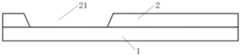
参照图2所示,为本申请提供的面板的一个实施例的结构示意图。由图可知,所述面板包括基板1、依次设置于所述基板1上的第一透明电极层3、绝缘层4以及设置于所述绝缘层4上的卷曲结构7;其中,所述卷曲结构7包括第二柔性电极层71且预设有卷曲的固有应力,使得在自然状态下,所述卷曲结构7能够卷曲起来,对所述第一透明电极层3和所述绝缘层4的透光性不造成任何遮挡作用;其中,所述固有应力可能分别来源于所述第二柔性电极层71和所述卷曲结构7中其他层的材料的不同热膨胀系数,或者由各层的制作方法(例如层沉积法)产生的。同时,基于现有技术中的卷曲结构卷曲后的局部高度将会远远超出平铺时的高度,形成突起,因此现有技术将会基于突起存在外因导致的损坏问题,由此,本实施例提出,参照图3d所示,所述第一透明电极层3和所述绝缘层4上对应形成有一个凹槽结构41;所述卷曲结构7设置于所述凹槽结构41内。这样使得所述卷曲结构7在卷曲状态时,也不会在所述绝缘层4表面形成凸起而出现容易损坏的问题。因此,本实施例所示面板能够克服现有技术存在的问题,提高面板电控的稳定性和有效性。Referring to FIG. 2 , it is a schematic structural diagram of an embodiment of the panel provided in the present application. As can be seen from the figure, the panel includes a
在本申请一些可选的实施例中,所述基板上形成有定位槽,所述第一透明电极层和所述绝缘层在所述定位槽上形成有凹槽结构;也即可以通过在基板上开设定位槽进而使得覆盖在基板上的第一透明电极层和所述绝缘层相应形成凹槽结构。优选的,所述第一透明电极层和所述绝缘层厚度保持均匀。这样,既可以保证凹槽结构位置的准确稳定,同时有利于各层级结构的贴合设计,保证安装效率。其中,所述基板可选为玻璃基板或者柔性塑料基板等,本实施例并不限制。In some optional embodiments of the present application, a positioning groove is formed on the substrate, and a groove structure is formed on the positioning groove for the first transparent electrode layer and the insulating layer; A positioning groove is formed on the substrate so that the first transparent electrode layer and the insulating layer covering the substrate form a corresponding groove structure. Preferably, the thicknesses of the first transparent electrode layer and the insulating layer are kept uniform. In this way, the accurate and stable position of the groove structure can be ensured, and at the same time, the fitting design of each level structure can be facilitated, and the installation efficiency can be ensured. The substrate may be optionally a glass substrate or a flexible plastic substrate, which is not limited in this embodiment.
或者,在另一些可选的实施例中,参照图2所示,还可以在所述基板1上设置有基质层2,所述基质层2上形成有定位槽21(如图3c),所述第一透明电极层3和所述绝缘层4依次设置于所述基质层2上且所述第一透明电极层和所述绝缘层在所述定位槽21上形成有凹槽结构41。其中,所述基质层2为树脂层,例如为有机透明树脂材料(Over Coat,OC)。需要说明的是,所述基质层2上的所示定位槽21既可以是贯通的凹槽结构使得对应基板表面露出,进而使得定位槽21中的第一透明电极层3贴附于基板上;也可以是非贯通槽,也即使得第一透明电极层3完全贴附于所述基质层上。Alternatively, in some other optional embodiments, referring to FIG. 2 , a
此外,上述凹槽结构也可以通过在所述绝缘层上挖槽形成,本申请实施例不做限制,只要在与所述卷曲结构接触的绝缘层上最终形成一个能够容纳所述卷曲结构的凹槽结构即可。In addition, the above-mentioned groove structure can also be formed by digging a groove on the insulating layer, which is not limited in the embodiment of the present application, as long as a groove capable of accommodating the curling structure is finally formed on the insulating layer in contact with the curling structure slot structure.
在本申请一些可选的实施例中,所述凹槽结构呈倒梯型且所述凹槽结构的深度大于或等于所述第二柔性电极层卷曲后形成的卷曲高度,也即所述卷曲结构卷曲在一起后形成的相对垂直于所述绝缘层表面的高度。这样通过凹槽结构呈倒梯型设计使得卷曲结构在延伸贴附到绝缘层上时,更容易从凹槽结构的两边缘往上延伸出去,也即能够更加容易爬坡。因此,进一步,可以将所述凹槽结构的边缘的坡度根据卷曲结构的爬坡需求相应的设计调整,并且在两个转角处设置更有利于贴合设计的弧度形状,以使得卷曲结构中的第二柔性电极层具有更好的贴合效果。In some optional embodiments of the present application, the groove structure is an inverted trapezoid, and the depth of the groove structure is greater than or equal to a curling height formed after the second flexible electrode layer is curled, that is, the curling The height relative to perpendicular to the surface of the insulating layer formed after the structures are crimped together. In this way, the inverted trapezoidal design of the groove structure makes it easier for the curled structure to extend upward from both edges of the groove structure when it is extended and attached to the insulating layer, that is, it is easier to climb the slope. Therefore, further, the slope of the edge of the groove structure can be adjusted according to the corresponding design according to the climbing requirements of the curling structure, and the two corners are provided with an arc shape that is more conducive to the design, so that the curling structure The second flexible electrode layer has a better fit effect.
参照图2和图3g可知,考虑到所述卷曲结构的支撑和稳定性问题,所述卷曲结构7还包括聚合物层72;所述第二柔性电极层71与所述聚合物层72贴合设置,且所述第二柔性电极层71与所述聚合物层72中的至少一层预设有卷曲的固有应力。这样不仅有利于卷曲结构的形成,同时能够基于所述聚合物层的功能给所述卷曲结构带来更好的优化,例如采用具有较好强度的聚合物层使得聚合物层与第二柔性电极层贴合形成的卷曲结构具有更好的强度,起到支撑作用;又例如还可以使用具有良好伸展性的聚合物层使得聚合物层与第二柔性电极层贴合形成的卷曲结构具有更好的伸展性,也即使得卷曲结构在伸展过程中更加稳定,不会由于第二柔性电极层过于柔软而出现起皱现象。其中,所述第一透明电极层3可选为透明电极,例如:ITO(indium tin oxid,氧化铟锡)、纳米银、铝锌氧化物的金属性材料或由聚苯胺以及聚(3,4乙烯二氧噻吩)聚(苯乙烯磺酸)的导电聚合物制成,例如:PEDOT:PSS(聚乙撑二氧噻吩-聚(苯乙烯磺酸盐))。所述绝缘层4可选为硅氮化物、硅氧化物或者聚合物材料,例如:聚酰亚胺、苯丙环丁烯等。所述第二柔性电极层71可选为铝、银等柔性电极。所述聚合物层72可选为柔性聚合物材料。Referring to FIG. 2 and FIG. 3g , considering the support and stability of the curled structure, the curled structure 7 further includes a
进一步优选的,所述聚合物层72设置于所述第二柔性电极层71远离所述第一透明电极层3的一侧。这样,可以使得第二柔性电极层71更加靠近所述第一透明电极层3进而使得两个电极层之间的电场更强,吸附作用力更大,进而更加有利于所述卷曲结构的延伸贴附到绝缘层上。Further preferably, the
此外,所述卷曲结构中还可以集成更多的层结构以实现更加复杂的功能,例如还可以增加光学功能层以实现光学功能,比如过滤或者光学发电等等。此外,这些增加的功能层既可以是额外增加的层级结构,也可以是直接将相应的功能集成到所述聚合物层72或者所述第二柔性电极层71中,本实施例不做限制。In addition, more layer structures can be integrated into the curled structure to realize more complex functions, for example, optical function layers can be added to realize optical functions, such as filtering or optical power generation. In addition, these added functional layers may be additionally added hierarchical structures, or may directly integrate corresponding functions into the
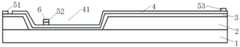
在本申请一些可选的实施例中,所述凹槽结构内设置有第一触点电极52;所述第二柔性电极层71的一端通过所述第一触点电极与所述绝缘层4固定连接;所述第一触点电极52用于给所述第二柔性电极层71供电。这样,一方面使得所述卷曲结构的一端具有固定接点以及使得所述固定接点处形成一定的坡度,更加有利于卷曲结构起始时刻的展开,另一方面能够保证对所述第二柔性电极层71的有效供电。其中,所述第一触点电极52可选的通过粘合剂6与所述第二柔性电极层71粘接。所述粘合剂6可选为ACF胶或其它导电胶。In some optional embodiments of the present application, the groove structure is provided with a
进一步,所述第一透明电极层3靠近所述凹槽结构41的一端设置有第二触点电极51;所述第二触点电极51用于给所述第一透明电极层3供电。这样既可以实现第一透明电极层3稳定有效的供电,而且不会对第二柔性电极层71造成干扰。Further, the end of the first
更进一步,所述绝缘层4远离所述凹槽结构的一端设置有第三触点电极53;所述第三触点电极53用于作为所述第二柔性电极层71展开时的定位结构。也即表示所述第二柔性电极层71展开到所述第三触点电极53位置即已完成延伸展开,同时起到信号反馈作用,例如在第三触点电极53设置有感应设备,当被施加电压的第二柔性电极层71靠近第三触点电极53时将会输出反馈信号,以使得控制部分知道所述第二柔性电极层71已完全展开。此外,所述第三触点电极还通过吸附第二柔性电极以实现更好的展开固定作用。Furthermore, a
具体的,以所述第一透明电极层3中通过所述第二触点电极51输入基准电压为例,当通过所述第一触点电极52向所述第二柔性电极层71输入爬坡电压时,所述第二柔性电极层71基于吸附作用逐渐沿所述第一透明电极层3伸展并且覆盖住所述第一透明电极层3,当所述第二柔性电极层71完全伸展时,所述第二柔性电极层71的活动端将与第三触点电极53吸附到一起,可以通过第三触点电极53与所述第二柔性电极层71的吸附增强伸展状态的维持,此时基于第二柔性电极层71的吸收或者反射作用,将使得面板不透光;若是撤销第三触点电极53以及第二柔性电极层71中的电压,则第二柔性电极层71基于固有应力回到卷曲状态,此时面板透光。相反,也可以向第二柔性电极层71中输入基准电压而向第一透明电极层3中输入爬坡电压,本实施例不再赘述。Specifically, taking the reference voltage input in the first
在本申请一些可选的实施例中,所述第三触点电极53对应所述凹槽结构的一侧设置有斜面结构(图中未显示)。也即可以在第二柔性电极层71于所述第三触点电极53相互接触的位置设置为斜面这样不仅有利于卷曲结构的伸展状态的保持,消除边缘位置的卷曲效应,同时还能够加快所述卷曲结构卷曲的效率,保证卷曲质量。In some optional embodiments of the present application, a side of the
优选的,所述第二柔性电极层71对应所述第三触点电极53的一端设置有与所述第三触点电极配合的端头结构(图中未显示)。这样可以使得所述第二柔性电极层71与第三触点电极53具有更加稳定的配合关系,例如可以在端部设置两个独立的磁性部件,通过磁性相吸使得所述第二柔性电极层71的端部与第三触点电极53连接更加稳定准确。当然,也可以采用其他形式配合结构,本实施例不做限制。Preferably, one end of the second
需要说明的是,上述实施例中的触点电极可选由非透明且较低电阻的金属组成,例如Mo,Al,Cu等。并且上述第一触点电极52、第二触点电极51以及第三触点电极53可选用同一种材料或者不同材料制备而成。It should be noted that, the contact electrodes in the above-mentioned embodiments may optionally be composed of non-transparent and relatively low-resistance metals, such as Mo, Al, Cu, and the like. In addition, the
在上述实施例的基础上,考虑到所述卷曲结构从凹槽底部到边缘的绝缘层需要经过一个由低位到高位的爬坡过程,因此需要不同的驱动力,由此,本申请提出将所述第一透明电极层设置为包括多个间隔排布的条状电极的结构,所述多个条状电极的排布方向与所述第二柔性电极层的伸展方向相同;其中,所述条状电极的排布方向为不同条状电极的间隔方向,也即使得条状电极大致沿垂直第二柔性电极层的伸展方向设置,然后向伸展方向间隔一段距离后重复设置多个条状电极。这样,可以通过给不同条状电极不同的驱动力进而实现不同阶段的延伸驱动,同时保证所述卷曲结构延伸的稳定性和可靠性。此外,条状电极还可以通过不同时间施加电压而使得能够有效控制所述卷曲结构的延伸状态,提高控制精度。例如可以使得第二柔性电极层只延伸一部分等。On the basis of the above-mentioned embodiment, considering that the insulating layer of the crimped structure from the bottom of the groove to the edge needs to go through a ramping process from low to high, different driving forces are required. The first transparent electrode layer is configured as a structure including a plurality of strip-shaped electrodes arranged at intervals, and the arrangement direction of the plurality of strip-shaped electrodes is the same as the extending direction of the second flexible electrode layer; wherein, the strips The arrangement direction of the strip electrodes is the spacing direction of different strip electrodes, that is, the strip electrodes are arranged approximately perpendicular to the stretching direction of the second flexible electrode layer, and then multiple strip electrodes are repeatedly arranged after a distance to the stretching direction. In this way, by giving different driving forces to different strip electrodes, different stages of extension driving can be realized, while ensuring the stability and reliability of the extension of the crimped structure. In addition, the strip electrodes can also apply voltages at different times, so that the extension state of the crimped structure can be effectively controlled, and the control accuracy can be improved. For example, only a part of the second flexible electrode layer can be extended.
实施例二,Example two,
本申请实施例还提供了一种调控装置,所述调控装置包括上述任一项实施例所述的面板。这样,能够将具有所述面板中电极结构的设计应用到不同的装置中,例如,所述调控装置可选为玻璃、门窗、以及各种需调光的平面等等,本申请不限制所述面板的具体应用领域。An embodiment of the present application further provides a control device, where the control device includes the panel described in any one of the foregoing embodiments. In this way, the design with the electrode structure in the panel can be applied to different devices, for example, the control device can be selected from glass, doors and windows, and various planes that need to be dimmed, etc. The application does not limit the The specific application area of the panel.
进一步,本申请实施例还提供了一种调控系统,所述调控系统包括上述任一项实施例所述的面板或所述调控装置;进一步还包括用于供电的电源以及用于控制所述第二柔性电极层伸展或者卷曲的控制单元。这样,可以通过调控系统中的控制单元实现面板或者调控装置的驱动控制,实现透光或者遮光的切换。Further, an embodiment of the present application also provides a control system, the control system includes the panel or the control device described in any of the above embodiments; further includes a power supply for power supply and a control system for controlling the first Two flexible electrode layers stretch or curl the control unit. In this way, the drive control of the panel or the control device can be realized through the control unit in the control system, and the switching of light transmission or shading can be realized.
实施例三,Example three,
本申请实施例还提供了一种所述面板的驱动方法,这里的驱动方法包括伸展驱动和卷曲驱动;其中,所述伸展驱动包括:The embodiment of the present application also provides a driving method of the panel, where the driving method includes stretching driving and curling driving; wherein, the stretching driving includes:
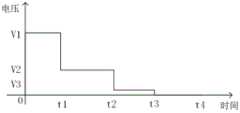
参照图4所示,为本申请提供的面板驱动方法的一个实施例中驱动电压示意图。首先,在所述第二柔性电极层位于所述凹槽结构内的第一阶段(0-t1),向所述第一透明电极层输入预设的基准电压,向所述第二柔性电极层输入预设的爬坡电压V1,通过基准电压与爬坡电压形成的电场驱动所述第二柔性电极层从所述凹槽结构内伸展出去;实现卷曲结构的爬坡。其中,这里的基准电压通常是指一个参考电压,一般可设置为0V。Referring to FIG. 4 , a schematic diagram of driving voltages in an embodiment of the panel driving method provided by the present application is shown. First, in the first stage (0-t1) when the second flexible electrode layer is located in the groove structure, a preset reference voltage is input to the first transparent electrode layer, and a preset reference voltage is input to the second flexible electrode layer A preset ramping voltage V1 is input, and the electric field formed by the reference voltage and the ramping voltage drives the second flexible electrode layer to stretch out from the groove structure; the ramping of the curling structure is realized. Among them, the reference voltage here usually refers to a reference voltage, which can generally be set to 0V.
其次,在所述第二柔性电极层至少部分离开所述凹槽结构内的第二阶段(t1-t2),向所述第二柔性电极层输入预设的舒展电压V2,舒展电压用于驱动所述第二柔性电极层沿紧靠所述第一透明电极层的方向伸展;其中,所述舒展电压小于所述爬坡电压;这样,通过在爬坡阶段输入相对较高的爬坡电压以方便卷曲结构能够快速爬坡舒展。这里的第二柔性电极层至少部分离开所述凹槽结构内是指所述第二柔性电极层通过伸展有部分已经脱离了凹槽结构范围内。Secondly, in the second stage (t1-t2) when the second flexible electrode layer is at least partially separated from the groove structure, a preset stretching voltage V2 is input to the second flexible electrode layer, and the stretching voltage is used for driving The second flexible electrode layer stretches in a direction close to the first transparent electrode layer; wherein, the stretch voltage is smaller than the ramp voltage; thus, by inputting a relatively high ramp voltage in the ramp stage, the The convenient crimping structure enables quick climbs and stretches. Here, the fact that the second flexible electrode layer is at least partially out of the groove structure means that the second flexible electrode layer has been partially out of the range of the groove structure by being stretched.
或者,还可以将两个电极层输入的电压调换,则可以如下:Alternatively, the input voltages of the two electrode layers can also be exchanged, as follows:
在所述第二柔性电极层位于所述凹槽结构内的第一阶段(0-t1),向所述第二柔性电极层输入预设的基准电压,向所述第一透明电极层输入预设的爬坡电压,所述爬坡电压用于驱动所述第二柔性电极层从所述凹槽结构内伸展出去;In the first stage (0-t1) when the second flexible electrode layer is located in the groove structure, a preset reference voltage is input to the second flexible electrode layer, and a preset reference voltage is input to the first transparent electrode layer. set ramping voltage, the ramping voltage is used to drive the second flexible electrode layer to stretch out from the groove structure;
在所述第二柔性电极层至少部分离开所述凹槽结构内的第二阶段(t1-t2),向所述第一透明电极层输入预设的舒展电压,所述舒展电压用于驱动所述第二柔性电极层沿紧靠所述第一透明电极层的方向伸展;其中,所述舒展电压小于所述爬坡电压;In the second stage (t1-t2) when the second flexible electrode layer is at least partially separated from the groove structure, a preset stretching voltage is input to the first transparent electrode layer, and the stretching voltage is used to drive the The second flexible electrode layer stretches in a direction close to the first transparent electrode layer; wherein, the stretch voltage is less than the ramp voltage;
所述卷曲驱动包括:The curling drive includes:
在需要卷曲的阶段,撤销所述第一透明电极层或所述第二柔性电极层中的至少一个的电压,使得所述第二柔性电极层在固有应力的作用下回卷到所述凹槽结构内。In the stage where curling is required, the voltage of at least one of the first transparent electrode layer or the second flexible electrode layer is withdrawn, so that the second flexible electrode layer is rolled back to the groove under the action of inherent stress within the structure.
参照图5所示,为本申请提供的面板驱动方法的另一个实施例中驱动电压示意图。由图可知,该实施例与图4所述实施例基本相同,不同之处在于增加了一个第三阶段,具体为:在所述第二柔性电极层完全伸展的第三阶段(t2-t3),向所述第二柔性电极层或者所述第一透明电极层输入预设的维持电压V3,维持电压用于驱动所述第二柔性电极层抵抗固有应力以维持伸展状态;其中,所述维持电压小于所述舒展电压。这样,可以使得卷曲结构仅仅需要一个较低的维持电压V3既可以保持伸展状态,大大降低了功耗。Referring to FIG. 5 , a schematic diagram of driving voltage in another embodiment of the panel driving method provided by the present application is shown. As can be seen from the figure, this embodiment is basically the same as the embodiment shown in FIG. 4 , except that a third stage is added, specifically: in the third stage (t2-t3) when the second flexible electrode layer is fully extended , input a preset maintaining voltage V3 to the second flexible electrode layer or the first transparent electrode layer, and the maintaining voltage is used to drive the second flexible electrode layer to resist the inherent stress to maintain the stretched state; wherein the maintaining The voltage is less than the stretch voltage. In this way, the curled structure can be maintained in the stretched state only with a lower sustaining voltage V3, which greatly reduces the power consumption.
进一步,针对于上述第一透明电极层采用间隔条状电极时,上述伸展驱动包括:向所述第一透明电极层输入控制电压时,根据所述第二柔性电极层的伸展位置向对应的条状电极输入控制电压或者改变对应的条状电极输入控制电压的大小;其中,多个间隔排布的条状电极为单独驱动电极;所述控制电压与所述第二柔性电极层中施加的电压对应形成抵抗所述第二柔性电极层固有应力的反作用力。这样可以通过条状电极实现更加准确的伸展驱动控制。Further, when the spacer strip electrodes are used for the first transparent electrode layer, the stretching driving includes: when a control voltage is input to the first transparent electrode layer, according to the stretching position of the second flexible electrode layer to the corresponding strip the input control voltage of the strip electrodes or change the magnitude of the corresponding strip electrodes input control voltage; wherein, a plurality of strip electrodes arranged at intervals are independent drive electrodes; the control voltage is the same as the voltage applied in the second flexible electrode layer A reaction force against the inherent stress of the second flexible electrode layer is correspondingly formed. In this way, more accurate stretch drive control can be achieved through the strip electrodes.
更具体的,例如:可以沿第二柔性电极层伸展方向设置多个独立控制的条状电极,当需要驱动第二柔性电极层沿延伸方向伸展时,可以依次向最靠近第二柔性电极层活动端的条状电极输入与第二柔性电极层匹配的控制电压,使得该条状电极与第二柔性电极层形成电场并驱动第二柔性电极层延伸,等到第二柔性电极层活动端超过当前条状电极时则可以撤销当前条状电极的电压而向沿延伸方向的下一个条状电极输入控制电压,使得第二柔性电极层逐步沿延伸方向伸展。当然,可以基于同样的原理,通过沿延伸方向依次给条状电极施加不同的电压而实现第二柔性电极层的驱动,同时可以向第二柔性电极层已覆盖区域的条状电极输入维持电压,使得第二柔性电极层已覆盖区域具有维持伸展的特性。进一步,针对于爬坡阶段也可以通过输入更大的电压来实现第二柔性电极层的爬坡过程。More specifically, for example, a plurality of independently controlled strip electrodes can be arranged along the extending direction of the second flexible electrode layer, and when the second flexible electrode layer needs to be driven to extend along the extending direction, the electrodes can be moved in sequence toward the closest to the second flexible electrode layer. The strip electrode at the end inputs a control voltage that matches the second flexible electrode layer, so that the strip electrode and the second flexible electrode layer form an electric field and drive the second flexible electrode layer to extend, until the active end of the second flexible electrode layer exceeds the current strip. When the electrode is used, the voltage of the current strip electrode can be canceled, and a control voltage can be input to the next strip electrode along the extension direction, so that the second flexible electrode layer is gradually extended along the extension direction. Of course, based on the same principle, the driving of the second flexible electrode layer can be realized by sequentially applying different voltages to the strip electrodes along the extending direction. The covered area of the second flexible electrode layer has the property of maintaining extension. Further, for the ramping stage, the ramping process of the second flexible electrode layer can also be implemented by inputting a larger voltage.
实施例四,本申请实施例还提供了一种所述面板的制备方法,参照图3a-3h所示,所述制备方法包括:
如图3a-3c所示,在基板上形成定位槽;其中,可以现在基板1上涂覆一层基质层2,然后通过曝光显影等工艺在基质层上形成定位槽21。当然,还可以直接在基板1上开设所示定位槽。As shown in Figures 3a-3c, positioning grooves are formed on the substrate; wherein, a
如图3d所示,在所述基板上依次形成第一透明电极层3和绝缘层4且使得所述第一透明电极层3和绝缘层4对应形成有凹槽结构41;As shown in FIG. 3d , a first
此时,如图3e和3f所示,可以分别在所述绝缘层的不同位置分别设置多个触点电极,第一触点电极52设置于凹槽结构41用于作为卷曲结构的连接点;第二触点电极51设置于第一透明电极层的端部,用于给第一透明电极层供电;第三触点电极53设置于所述绝缘层远离凹槽结构的一端,用于作为卷曲结构伸展的定位点或者锁定点。At this time, as shown in FIGS. 3e and 3f, a plurality of contact electrodes can be respectively provided at different positions of the insulating layer, and the
参照图3g-3h所示,将包含有第二柔性电极层的卷曲结构的一端设置在所述凹槽结构中;其中,所述卷曲结构预设有卷曲的固有应力。其中,如图3g所示,可以预先将第二柔性电极层71贴附于聚合物层72上,然后使得卷曲结构通过粘合剂6与第一触点电极52粘接。Referring to FIGS. 3g-3h, one end of the crimp structure including the second flexible electrode layer is disposed in the groove structure; wherein, the crimp structure is preset with the inherent stress of the crimp. Wherein, as shown in FIG. 3g , the second
这里的卷曲结构在平展状态时如图3h所示,在第一透明电极层3和第二柔性电极层71之间施加电场,使得卷曲结构7由于电场力作用而铺展,且在绝缘层4上采取拉伸的平面姿态。The curled structure here is in the flat state as shown in FIG. 3h , an electric field is applied between the first
卷曲结构为卷曲状态时如图2所示,当在第一透明电极层3和第二柔性电极层71之间施加电场去掉后,静电力消除并且卷曲结构7由于固有应力而恢复到其卷曲姿态。When the curled structure is in a curled state, as shown in FIG. 2 , when the electric field applied between the first
由上述实施例可知,本申请主要通过下层结构设计,将电极凸起部分进行找平,然后通过多台阶电压驱动进行聚合物的开合和关闭。同时采用多级驱动方式来有效配合该卷曲结构的爬坡、舒展、保持及回缩等不同过程。解决了使用聚合物的方式来实现光的透过和遮挡中的凸起物可能受外力破环的问题,提升了产品良率,与此同时还降低了功耗。It can be seen from the above embodiments that the present application mainly uses the design of the underlying structure to level the protruding portion of the electrode, and then drives the polymer to open, close and close through multi-step voltage driving. At the same time, a multi-stage driving method is adopted to effectively cooperate with the different processes of the curling structure, such as climbing, stretching, maintaining and retracting. It solves the problem that the protrusions in the transmission and shading of light may be damaged by external force by using the polymer method, which improves the product yield and reduces the power consumption at the same time.
所属领域的普通技术人员应当理解:以上任何实施例的讨论仅为示例性的,并非旨在暗示本公开的范围(包括权利要求)被限于这些例子;在本发明的思路下,以上实施例或者不同实施例中的技术特征之间也可以进行组合,步骤可以以任意顺序实现,并存在如上所述的本发明的不同方面的许多其它变化,为了简明它们没有在细节中提供。Those of ordinary skill in the art should understand that the discussion of any of the above embodiments is only exemplary, and is not intended to imply that the scope of the present disclosure (including the claims) is limited to these examples; under the spirit of the present invention, the above embodiments or There may also be combinations between technical features in different embodiments, steps may be carried out in any order, and there are many other variations of the different aspects of the invention as described above, which are not provided in detail for the sake of brevity.
另外,为简化说明和讨论,并且为了不会使本发明难以理解,在所提供的附图中可以示出或可以不示出与集成电路(IC)芯片和其它部件的公知的电源/接地连接。此外,可以以框图的形式示出装置,以便避免使本发明难以理解,并且这也考虑了以下事实,即关于这些框图装置的实施方式的细节是高度取决于将要实施本发明的平台的(即,这些细节应当完全处于本领域技术人员的理解范围内)。在阐述了具体细节(例如,电路)以描述本发明的示例性实施例的情况下,对本领域技术人员来说显而易见的是,可以在没有这些具体细节的情况下或者这些具体细节有变化的情况下实施本发明。因此,这些描述应被认为是说明性的而不是限制性的。Additionally, well known power/ground connections to integrated circuit (IC) chips and other components may or may not be shown in the figures provided in order to simplify illustration and discussion, and in order not to obscure the present invention. . Furthermore, devices may be shown in block diagram form in order to avoid obscuring the present invention, and this also takes into account the fact that the details of the implementation of these block diagram devices are highly dependent on the platform on which the invention will be implemented (i.e. , these details should be fully within the understanding of those skilled in the art). Where specific details (eg, circuits) are set forth to describe exemplary embodiments of the invention, it will be apparent to those skilled in the art that these specific details may be made without or with changes The present invention is carried out below. Accordingly, these descriptions are to be regarded as illustrative rather than restrictive.
尽管已经结合了本发明的具体实施例对本发明进行了描述,但是根据前面的描述,这些实施例的很多替换、修改和变型对本领域普通技术人员来说将是显而易见的。例如,其它存储器架构(例如,动态RAM(DRAM))可以使用所讨论的实施例。Although the present invention has been described in conjunction with specific embodiments thereof, many alternatives, modifications, and variations to these embodiments will be apparent to those of ordinary skill in the art from the foregoing description. For example, other memory architectures (eg, dynamic RAM (DRAM)) may use the discussed embodiments.
本发明的实施例旨在涵盖落入所附权利要求的宽泛范围之内的所有这样的替换、修改和变型。因此,凡在本发明的精神和原则之内,所做的任何省略、修改、等同替换、改进等,均应包含在本发明的保护范围之内。Embodiments of the present invention are intended to cover all such alternatives, modifications and variations that fall within the broad scope of the appended claims. Therefore, any omission, modification, equivalent replacement, improvement, etc. made within the spirit and principle of the present invention shall be included within the protection scope of the present invention.
Claims (18)
Priority Applications (2)
| Application Number | Priority Date | Filing Date | Title |
|---|---|---|---|
| CN201811024606.3ACN109031839B (en) | 2018-09-04 | 2018-09-04 | A panel, driving method, preparation method, regulating device and regulating system |
| US16/397,625US11237383B2 (en) | 2018-09-04 | 2019-04-29 | Dimming panel and driving method, preparation method thereof, controlling device and controlling system |
Applications Claiming Priority (1)
| Application Number | Priority Date | Filing Date | Title |
|---|---|---|---|
| CN201811024606.3ACN109031839B (en) | 2018-09-04 | 2018-09-04 | A panel, driving method, preparation method, regulating device and regulating system |
Publications (2)
| Publication Number | Publication Date |
|---|---|
| CN109031839A CN109031839A (en) | 2018-12-18 |
| CN109031839Btrue CN109031839B (en) | 2021-03-09 |
Family
ID=64623189
Family Applications (1)
| Application Number | Title | Priority Date | Filing Date |
|---|---|---|---|
| CN201811024606.3AActiveCN109031839B (en) | 2018-09-04 | 2018-09-04 | A panel, driving method, preparation method, regulating device and regulating system |
Country Status (2)
| Country | Link |
|---|---|
| US (1) | US11237383B2 (en) |
| CN (1) | CN109031839B (en) |
Families Citing this family (1)
| Publication number | Priority date | Publication date | Assignee | Title |
|---|---|---|---|---|
| CN109709695B (en)* | 2019-01-10 | 2021-12-24 | 京东方科技集团股份有限公司 | Display substrate, manufacturing method thereof and display device |
Citations (6)
| Publication number | Priority date | Publication date | Assignee | Title |
|---|---|---|---|---|
| CN85106866A (en)* | 1985-09-12 | 1987-03-11 | 乔治·R·辛普森 | Electrostatically actuated two-state device array and method of manufacture |
| CN1166610A (en)* | 1995-08-22 | 1997-12-03 | 大宇电子株式会社 | Method for formation of thin film actuated mirror array |
| JP2000315820A (en)* | 1999-04-27 | 2000-11-14 | Shogen Koden Kofun Yugenkoshi | High intensity light emitting diode |
| CN1836469A (en)* | 2003-06-13 | 2006-09-20 | 株式会社丰田自动织机 | EL device, manufacturing method of same, and liquid crystal display device using EL device |
| JP2012053474A (en)* | 2005-02-23 | 2012-03-15 | Pixtronix Inc | Display device |
| JP2016503513A (en)* | 2012-10-30 | 2016-02-04 | ピクストロニクス,インコーポレイテッド | Display device using complex composition colors unique to frames |
Family Cites Families (5)
| Publication number | Priority date | Publication date | Assignee | Title |
|---|---|---|---|---|
| US7110163B2 (en)* | 2001-07-09 | 2006-09-19 | E Ink Corporation | Electro-optic display and lamination adhesive for use therein |
| DE602005001853T2 (en)* | 2004-02-04 | 2008-04-17 | Koninklijke Philips Electronics N.V. | MECHANICAL STRUCTURE WITH A LAYER OF POLYMERIZED LIQUID CRYSTAL AND METHOD OF MANUFACTURING THEREOF |
| US20100001666A1 (en)* | 2006-12-21 | 2010-01-07 | Koninklijke Philips Electronics N.V. | Micro-electro-mechanical system with actuators |
| WO2016049759A1 (en)* | 2014-09-29 | 2016-04-07 | Aero-Shade Technologies Canada, Inc. | Light blocking microshutter |
| JP2016091841A (en)* | 2014-11-06 | 2016-05-23 | 株式会社Joled | Organic light-emitting device and organic display device |
- 2018
- 2018-09-04CNCN201811024606.3Apatent/CN109031839B/enactiveActive
- 2019
- 2019-04-29USUS16/397,625patent/US11237383B2/enactiveActive
Patent Citations (6)
| Publication number | Priority date | Publication date | Assignee | Title |
|---|---|---|---|---|
| CN85106866A (en)* | 1985-09-12 | 1987-03-11 | 乔治·R·辛普森 | Electrostatically actuated two-state device array and method of manufacture |
| CN1166610A (en)* | 1995-08-22 | 1997-12-03 | 大宇电子株式会社 | Method for formation of thin film actuated mirror array |
| JP2000315820A (en)* | 1999-04-27 | 2000-11-14 | Shogen Koden Kofun Yugenkoshi | High intensity light emitting diode |
| CN1836469A (en)* | 2003-06-13 | 2006-09-20 | 株式会社丰田自动织机 | EL device, manufacturing method of same, and liquid crystal display device using EL device |
| JP2012053474A (en)* | 2005-02-23 | 2012-03-15 | Pixtronix Inc | Display device |
| JP2016503513A (en)* | 2012-10-30 | 2016-02-04 | ピクストロニクス,インコーポレイテッド | Display device using complex composition colors unique to frames |
Also Published As
| Publication number | Publication date |
|---|---|
| US20200073112A1 (en) | 2020-03-05 |
| US11237383B2 (en) | 2022-02-01 |
| CN109031839A (en) | 2018-12-18 |
Similar Documents
| Publication | Publication Date | Title |
|---|---|---|
| US8134112B2 (en) | Method of fabricating an insulated glazing unit having controllable radiation transmittance | |
| JP7277479B2 (en) | Potential Driven Shade Including Shutters Supporting Surface Modified Conductive Coatings, Methods of Manufacture, and Methods of Operation | |
| KR102108830B1 (en) | Electrochromic Device | |
| JP7185707B2 (en) | Potential Driven Shade Including Shutters Supporting Surface Modified Conductive Coatings, Methods of Manufacture, and Methods of Operation | |
| CN112684619A (en) | Local erasing liquid crystal writing device and method based on photosensitive switch element | |
| BR112020022813B1 (en) | POTENTIALLY ACTIVATED ELECTRIC CURTAIN INCLUDING CONDUCTIVE COATING MODIFIED BY SLEEVE SUPPORT SURFACE, METHODS FOR MANUFACTURING THE SAME AND METHOD OF OPERATION | |
| JP2021520461A (en) | Electrically and potentially driven shades with improved coil strength, how they are manufactured, and how they operate | |
| JP2021529900A (en) | Potential drive shade with improved coil strength, its manufacturing method, and its operating method | |
| CN110033900A (en) | Flexible conductive film and preparation method thereof, display panel | |
| TWI629538B (en) | Transmissivity-changeable film and method of manufacturing the same | |
| US20200124900A1 (en) | Flexible liquid crystal optical shutter and manufacturing method thereof | |
| US20170220160A1 (en) | Touch Panel, Method for Manufacturing the Same and Touch Display Panel | |
| BR112020022051A2 (en) | potentially driven electric curtain with improved coil resistance, method of manufacturing it and method of operating it | |
| CN108776405B (en) | Multi-state smart window, preparation method thereof, and multi-pattern smart window prepared therefrom | |
| CN109031839B (en) | A panel, driving method, preparation method, regulating device and regulating system | |
| KR20220129537A (en) | Potentially driven shades with electrostatic shade kickback, and/or associated methods | |
| JP2023512979A (en) | Potential Driven Shade Coil Distortion Correction Techniques and/or Related Methods | |
| CN114665859B (en) | An infrared optical switch based on thermoelectric co-regulation of vanadium dioxide thin film | |
| KR20150029395A (en) | Hybrid touch sensing electrode and preparing method thereof | |
| CN103529616A (en) | Electronic paper display module and device with touch function | |
| CN107015705A (en) | A kind of touch control display apparatus, contact panel and preparation method thereof | |
| CN109002236A (en) | A kind of flexible touch screen, its production method and display device | |
| CN115421335B (en) | Dimming panel, preparation method thereof, dimming device, dimming system and vehicle | |
| CN211928367U (en) | Electrochromic laminated glass with electric heating function and electrochromic hollow glass | |
| CN107359212A (en) | Electrically conducting transparent substrate, its preparation method and solar cell |
Legal Events
| Date | Code | Title | Description |
|---|---|---|---|
| PB01 | Publication | ||
| PB01 | Publication | ||
| SE01 | Entry into force of request for substantive examination | ||
| SE01 | Entry into force of request for substantive examination | ||
| GR01 | Patent grant | ||
| GR01 | Patent grant |