CN109002236B - Flexible touch screen, manufacturing method thereof and display device - Google Patents
Flexible touch screen, manufacturing method thereof and display deviceDownload PDFInfo
- Publication number
- CN109002236B CN109002236BCN201810803180.5ACN201810803180ACN109002236BCN 109002236 BCN109002236 BCN 109002236BCN 201810803180 ACN201810803180 ACN 201810803180ACN 109002236 BCN109002236 BCN 109002236B
- Authority
- CN
- China
- Prior art keywords
- protective layer
- flexible
- layer
- flexible substrate
- substrate
- Prior art date
- Legal status (The legal status is an assumption and is not a legal conclusion. Google has not performed a legal analysis and makes no representation as to the accuracy of the status listed.)
- Expired - Fee Related
Links
Images


Classifications
- G—PHYSICS
- G06—COMPUTING OR CALCULATING; COUNTING
- G06F—ELECTRIC DIGITAL DATA PROCESSING
- G06F3/00—Input arrangements for transferring data to be processed into a form capable of being handled by the computer; Output arrangements for transferring data from processing unit to output unit, e.g. interface arrangements
- G06F3/01—Input arrangements or combined input and output arrangements for interaction between user and computer
- G06F3/03—Arrangements for converting the position or the displacement of a member into a coded form
- G06F3/041—Digitisers, e.g. for touch screens or touch pads, characterised by the transducing means
- G06F3/0412—Digitisers structurally integrated in a display
- G—PHYSICS
- G06—COMPUTING OR CALCULATING; COUNTING
- G06F—ELECTRIC DIGITAL DATA PROCESSING
- G06F3/00—Input arrangements for transferring data to be processed into a form capable of being handled by the computer; Output arrangements for transferring data from processing unit to output unit, e.g. interface arrangements
- G06F3/01—Input arrangements or combined input and output arrangements for interaction between user and computer
- G06F3/03—Arrangements for converting the position or the displacement of a member into a coded form
- G06F3/041—Digitisers, e.g. for touch screens or touch pads, characterised by the transducing means
- G06F3/044—Digitisers, e.g. for touch screens or touch pads, characterised by the transducing means by capacitive means
- H—ELECTRICITY
- H10—SEMICONDUCTOR DEVICES; ELECTRIC SOLID-STATE DEVICES NOT OTHERWISE PROVIDED FOR
- H10K—ORGANIC ELECTRIC SOLID-STATE DEVICES
- H10K71/00—Manufacture or treatment specially adapted for the organic devices covered by this subclass
- H10K71/80—Manufacture or treatment specially adapted for the organic devices covered by this subclass using temporary substrates
- H—ELECTRICITY
- H10—SEMICONDUCTOR DEVICES; ELECTRIC SOLID-STATE DEVICES NOT OTHERWISE PROVIDED FOR
- H10K—ORGANIC ELECTRIC SOLID-STATE DEVICES
- H10K77/00—Constructional details of devices covered by this subclass and not covered by groups H10K10/80, H10K30/80, H10K50/80 or H10K59/80
- H10K77/10—Substrates, e.g. flexible substrates
- H10K77/111—Flexible substrates
- G—PHYSICS
- G06—COMPUTING OR CALCULATING; COUNTING
- G06F—ELECTRIC DIGITAL DATA PROCESSING
- G06F2203/00—Indexing scheme relating to G06F3/00 - G06F3/048
- G06F2203/041—Indexing scheme relating to G06F3/041 - G06F3/045
- G06F2203/04102—Flexible digitiser, i.e. constructional details for allowing the whole digitising part of a device to be flexed or rolled like a sheet of paper
- G—PHYSICS
- G06—COMPUTING OR CALCULATING; COUNTING
- G06F—ELECTRIC DIGITAL DATA PROCESSING
- G06F2203/00—Indexing scheme relating to G06F3/00 - G06F3/048
- G06F2203/041—Indexing scheme relating to G06F3/041 - G06F3/045
- G06F2203/04103—Manufacturing, i.e. details related to manufacturing processes specially suited for touch sensitive devices
- H—ELECTRICITY
- H10—SEMICONDUCTOR DEVICES; ELECTRIC SOLID-STATE DEVICES NOT OTHERWISE PROVIDED FOR
- H10D—INORGANIC ELECTRIC SEMICONDUCTOR DEVICES
- H10D86/00—Integrated devices formed in or on insulating or conducting substrates, e.g. formed in silicon-on-insulator [SOI] substrates or on stainless steel or glass substrates
- H10D86/01—Manufacture or treatment
- H10D86/021—Manufacture or treatment of multiple TFTs
- H10D86/0214—Manufacture or treatment of multiple TFTs using temporary substrates
- H—ELECTRICITY
- H10—SEMICONDUCTOR DEVICES; ELECTRIC SOLID-STATE DEVICES NOT OTHERWISE PROVIDED FOR
- H10K—ORGANIC ELECTRIC SOLID-STATE DEVICES
- H10K2102/00—Constructional details relating to the organic devices covered by this subclass
- H10K2102/301—Details of OLEDs
- H10K2102/311—Flexible OLED
- Y—GENERAL TAGGING OF NEW TECHNOLOGICAL DEVELOPMENTS; GENERAL TAGGING OF CROSS-SECTIONAL TECHNOLOGIES SPANNING OVER SEVERAL SECTIONS OF THE IPC; TECHNICAL SUBJECTS COVERED BY FORMER USPC CROSS-REFERENCE ART COLLECTIONS [XRACs] AND DIGESTS
- Y02—TECHNOLOGIES OR APPLICATIONS FOR MITIGATION OR ADAPTATION AGAINST CLIMATE CHANGE
- Y02E—REDUCTION OF GREENHOUSE GAS [GHG] EMISSIONS, RELATED TO ENERGY GENERATION, TRANSMISSION OR DISTRIBUTION
- Y02E10/00—Energy generation through renewable energy sources
- Y02E10/50—Photovoltaic [PV] energy
- Y02E10/549—Organic PV cells
- Y—GENERAL TAGGING OF NEW TECHNOLOGICAL DEVELOPMENTS; GENERAL TAGGING OF CROSS-SECTIONAL TECHNOLOGIES SPANNING OVER SEVERAL SECTIONS OF THE IPC; TECHNICAL SUBJECTS COVERED BY FORMER USPC CROSS-REFERENCE ART COLLECTIONS [XRACs] AND DIGESTS
- Y02—TECHNOLOGIES OR APPLICATIONS FOR MITIGATION OR ADAPTATION AGAINST CLIMATE CHANGE
- Y02P—CLIMATE CHANGE MITIGATION TECHNOLOGIES IN THE PRODUCTION OR PROCESSING OF GOODS
- Y02P70/00—Climate change mitigation technologies in the production process for final industrial or consumer products
- Y02P70/50—Manufacturing or production processes characterised by the final manufactured product
Landscapes
- Engineering & Computer Science (AREA)
- General Engineering & Computer Science (AREA)
- Theoretical Computer Science (AREA)
- Human Computer Interaction (AREA)
- Physics & Mathematics (AREA)
- General Physics & Mathematics (AREA)
- Manufacturing & Machinery (AREA)
- Position Input By Displaying (AREA)
Abstract
Translated fromChinese
Description
Translated fromChinese技术领域technical field
本发明涉及触控显示技术领域,尤指一种柔性触摸屏、其制作方法及显示装置。The present invention relates to the technical field of touch display, in particular to a flexible touch screen, a manufacturing method thereof and a display device.
背景技术Background technique
随着显示技术的迅速发展,有机发光二极管显示器(Organic Light-EmittingDiode,OLED)逐步成为当前电子显示的热点,OLED显示器的原理为自发光技术,即采用电子-空穴填充导致电子能级跃迁发光。OLED显示器率先应用在手机产上,目前市面上很多高档手机产品采用OLED显示器,例如三星手机的S6/S7/S8型号,OPPO手机的R9型号等。另外,应OLED显示器发展而孕育出来的柔性触摸屏已逐步推广在OLED显示领域。With the rapid development of display technology, organic light-emitting diode displays (Organic Light-Emitting Diode, OLED) have gradually become a hot spot in current electronic displays. The principle of OLED displays is self-luminous technology, that is, the use of electron-hole filling to cause electron energy level transition to emit light . OLED displays are the first to be used in mobile phone production. At present, many high-end mobile phone products on the market use OLED displays, such as the S6/S7/S8 models of Samsung mobile phones and the R9 model of OPPO mobile phones. In addition, the flexible touch screen bred in response to the development of OLED displays has been gradually promoted in the field of OLED displays.
在现有技术中,由于产品良率、莫尔纹现象以及透过率等因素的影响,使得金属材料制作的触控电极存在很多缺点,而透明导电氧化物制作的触控电极的导电性和透过率都比较好,例如可以采用氧化铟锡(Indium tin oxide,ITO)制作触控电极,这种透明导电材料制作的柔性触摸屏将在很长时间内占据OLED显示器的市场份额。随着全屏手机的大力发展,要求柔性触摸屏具有窄边框甚至无边框,这就需要触控电极具有更低的方阻,才能使驱动芯片(IC)具备驱动能力。另外,为了降低OLED显示器在触摸屏上的功耗,也要求触控电极向低方阻值的方向发展。In the prior art, due to the influence of factors such as product yield, moire phenomenon and transmittance, the touch electrodes made of metal materials have many disadvantages, while the conductivity of the touch electrodes made of transparent conductive oxides The transmittance is relatively good. For example, indium tin oxide (ITO) can be used to make touch electrodes. The flexible touch screen made of this transparent conductive material will occupy the market share of OLED displays for a long time. With the vigorous development of full-screen mobile phones, flexible touch screens are required to have narrow or even no borders, which requires the touch electrodes to have lower square resistance, so that the driver chip (IC) can have the driving ability. In addition, in order to reduce the power consumption of the OLED display on the touch screen, the touch electrodes are also required to develop in the direction of low square resistance.
然而,由于要求柔性触摸屏的触控电极具有较低的方阻,这就需要增加制作触控电极的透明导电氧化物薄膜的厚度,透明导电氧化物薄膜的厚度增大会导致透明导电氧化物薄膜的压应力增大,而且柔性基底一般都比较薄,在制作完成后,将柔性触摸屏从衬底基板上撕下来时,柔性触摸屏容易卷曲,从而影响柔性触摸屏的良率。However, since the touch electrodes of the flexible touch screen are required to have low square resistance, it is necessary to increase the thickness of the transparent conductive oxide film used to make the touch electrodes. The compressive stress increases, and the flexible substrate is generally relatively thin. After the flexible touch screen is torn off from the substrate substrate, the flexible touch screen is easily curled, thereby affecting the yield of the flexible touch screen.
发明内容SUMMARY OF THE INVENTION
本发明实施例提供一种柔性触摸屏、其制作方法及显示装置,用以解决现有技术中存在的柔性触摸屏在制作过程中容易出现卷曲的问题。Embodiments of the present invention provide a flexible touch screen, a manufacturing method thereof, and a display device, so as to solve the problem that the flexible touch screen in the prior art is prone to curling during the manufacturing process.
第一方面,本发明实施例提供了一种柔性触摸屏的制作方法,包括:In a first aspect, an embodiment of the present invention provides a method for manufacturing a flexible touch screen, including:
在柔性基材的表面贴附一层第一保护层;A first protective layer is attached to the surface of the flexible substrate;
将所述柔性基材背离所述第一保护层一侧的表面贴附于衬底基板上;attaching the surface of the flexible substrate away from the first protective layer on the base substrate;
去除所述第一保护层;removing the first protective layer;
在所述柔性基材背离所述衬底基板的一侧形成触控电极层;forming a touch electrode layer on the side of the flexible substrate away from the base substrate;
在所述触控电极层的表面贴附一层第二保护层;A second protective layer is attached on the surface of the touch electrode layer;
将所述柔性基材与所述衬底基板分离;separating the flexible substrate from the base substrate;
去除所述第二保护层。The second protective layer is removed.
在一种可能的实现方式中,在本发明实施例提供的上述制作方法中,所述第一保护层的热膨胀系数与所述柔性基材的热膨胀系数的差异小于0.05%;In a possible implementation manner, in the above manufacturing method provided by the embodiment of the present invention, the difference between the thermal expansion coefficient of the first protective layer and the thermal expansion coefficient of the flexible substrate is less than 0.05%;
所述第二保护层的热膨胀系数与所述柔性基材的热膨胀系数的差异小于0.05%。The difference between the thermal expansion coefficient of the second protective layer and the thermal expansion coefficient of the flexible substrate is less than 0.05%.
在一种可能的实现方式中,在本发明实施例提供的上述制作方法中,所述第一保护层的材料为酚醛树脂、聚对苯二甲酸乙二醇酯或环烯烃聚合物;In a possible implementation manner, in the above-mentioned manufacturing method provided by the embodiment of the present invention, the material of the first protective layer is phenolic resin, polyethylene terephthalate or cycloolefin polymer;
所述第二保护层的材料为酚醛树脂、聚对苯二甲酸乙二醇酯或环烯烃聚合物。The material of the second protective layer is phenolic resin, polyethylene terephthalate or cycloolefin polymer.
在一种可能的实现方式中,在本发明实施例提供的上述制作方法中,所述将所述柔性基材背离所述第一保护层一侧的表面贴附于衬底基板上,包括:In a possible implementation manner, in the above-mentioned manufacturing method provided by the embodiment of the present invention, the step of attaching the surface of the flexible base material on the side away from the first protective layer on the base substrate includes:
在所述衬底基板上形成一层温控粘合层;forming a temperature control adhesive layer on the base substrate;
通过所述温控粘合层将所述柔性基材贴附于所述衬底基板上。The flexible substrate is attached to the base substrate through the temperature control adhesive layer.
在一种可能的实现方式中,在本发明实施例提供的上述制作方法中,所述去除所述第二保护层,包括:In a possible implementation manner, in the above manufacturing method provided by the embodiment of the present invention, the removing the second protective layer includes:
对形成所述触控电极层的所述柔性基材进行切割后,去除所述第二保护层。After cutting the flexible substrate on which the touch electrode layer is formed, the second protective layer is removed.
在一种可能的实现方式中,在本发明实施例提供的上述制作方法中,所述在柔性基材的表面贴附一层第一保护层之前,还包括:In a possible implementation manner, in the above-mentioned manufacturing method provided by the embodiment of the present invention, before attaching a first protective layer to the surface of the flexible substrate, the method further includes:
在所述柔性基材的两个表面上分别形成一层硬化层。A hardened layer is respectively formed on both surfaces of the flexible substrate.
在一种可能的实现方式中,在本发明实施例提供的上述制作方法中,所述在柔性基材的表面贴附一层第一保护层,包括:In a possible implementation manner, in the above-mentioned manufacturing method provided by the embodiment of the present invention, the method of attaching a first protective layer to the surface of the flexible substrate includes:
在所述柔性基材的任意一侧的表面上形成一层消影层;forming an erasing layer on the surface of either side of the flexible substrate;
在所述消影层之上贴附一层所述第一保护层。A layer of the first protective layer is attached on the erasing layer.
在一种可能的实现方式中,在本发明实施例提供的上述制作方法中,所述在所述柔性基材背离所述衬底基板的一侧形成触控电极层,包括:In a possible implementation manner, in the above-mentioned manufacturing method provided by the embodiment of the present invention, the forming the touch electrode layer on the side of the flexible substrate away from the base substrate includes:
在所述柔性基材背离所述衬底基板的一侧形成多个第一触控电极和多个第二触控电极;所述第一触控电极与所述第二触控电极相互交叉,所述第一触控电极为条状结构,所述第二触控电极包括多个子电极;A plurality of first touch electrodes and a plurality of second touch electrodes are formed on the side of the flexible substrate away from the base substrate; the first touch electrodes and the second touch electrodes cross each other, The first touch electrodes are strip-shaped structures, and the second touch electrodes include a plurality of sub-electrodes;
形成多条信号线;所述信号线与所述第一触控电极或所述第二触控电极连接;forming a plurality of signal lines; the signal lines are connected with the first touch electrodes or the second touch electrodes;
在所述信号线所在膜层之上形成一层绝缘层;forming an insulating layer on the film layer where the signal line is located;
在所述绝缘层之上形成多个桥接线;所述桥接线用于连接所述第二触控电极中的各所述子电极。A plurality of bridge lines are formed on the insulating layer; the bridge lines are used for connecting each of the sub-electrodes in the second touch electrodes.
第二方面,本发明实施例提供了一种柔性触摸屏,所述柔性触摸屏上述柔性触摸屏的制作方法制作而成。In a second aspect, an embodiment of the present invention provides a flexible touch screen manufactured by the above-mentioned manufacturing method of the flexible touch screen.
第三方面,本发明实施例提供了一种显示装置,包括:上述柔性触摸屏。In a third aspect, an embodiment of the present invention provides a display device, including: the above-mentioned flexible touch screen.
本发明有益效果如下:The beneficial effects of the present invention are as follows:
本发明实施例提供的柔性触摸屏、其制作方法及显示装置,该制作方法,包括:在柔性基材的表面贴附一层第一保护层;将柔性基材背离第一保护层一侧的表面贴附于衬底基板上;去除第一保护层;在柔性基材背离衬底基板的一侧形成触控电极层;在触控电极层的表面贴附一层第二保护层;将柔性基材与衬底基板分离;去除第二保护层。本发明实施例提供的柔性触摸屏的制作方法,将柔性基材贴附于衬底基板之前,在柔性基材的表面贴附一层第一保护层,第一保护层起到支撑作用,可以使柔性基材平整的贴附于衬底基板上,并在柔性基材贴附于衬底基板上之后去除第一保护层,不会影响柔性触摸屏的结构,此外,在制作触控电极层之后再贴附一层第二保护层,从而使柔性基材与衬底基板分离时,柔性基材不会发生卷曲,提高了产品良率。Embodiments of the present invention provide a flexible touch screen, a manufacturing method thereof, and a display device. The manufacturing method includes: attaching a first protective layer on the surface of a flexible substrate; and attaching a surface of the flexible substrate away from the first protective layer Affixing on the base substrate; removing the first protective layer; forming a touch electrode layer on the side of the flexible base material away from the base substrate; attaching a second protective layer on the surface of the touch electrode layer; The material is separated from the base substrate; the second protective layer is removed. In the manufacturing method of the flexible touch screen provided by the embodiment of the present invention, before attaching the flexible substrate to the base substrate, a first protective layer is attached to the surface of the flexible substrate, and the first protective layer plays a supporting role, which can make The flexible substrate is flatly attached to the base substrate, and the first protective layer is removed after the flexible substrate is attached to the base substrate, which will not affect the structure of the flexible touch screen. A second protective layer is attached, so that when the flexible substrate is separated from the base substrate, the flexible substrate will not be curled, thereby improving the product yield.
附图说明Description of drawings
图1为本发明实施例提供的上述柔性触摸屏的制作方法的流程图;FIG. 1 is a flowchart of a method for manufacturing the above-mentioned flexible touch screen provided by an embodiment of the present invention;
图2a至图2g为本发明实施例提供的上述制作方法对应的一种流程结构示意图;2a to 2g are schematic structural diagrams of a process corresponding to the above-mentioned manufacturing method provided by an embodiment of the present invention;
图3a至图3m为本发明实施例提供的上述制作方法对应的另一种流程结构示意图;3a to 3m are schematic diagrams of another process structure corresponding to the above-mentioned manufacturing method provided by an embodiment of the present invention;
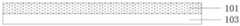
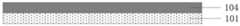
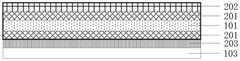
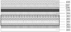
其中,101、柔性衬底;102、第一保护层;103、衬底基板;104、触控电极层;105、第二保护层;201、硬化层;202、消影层;203、温度粘合层;204、第一透明导电层;205、金属层;206、绝缘层;207、第二透明导电层。101, flexible substrate; 102, first protective layer; 103, base substrate; 104, touch electrode layer; 105, second protective layer; 201, hardening layer; 202, erasing layer; 203, temperature adhesive 204, the first transparent conductive layer; 205, the metal layer; 206, the insulating layer; 207, the second transparent conductive layer.
具体实施方式Detailed ways
针对现有技术中存在的柔性触摸屏在制作过程中容易出现卷曲的问题,本发明实施例提供了一种柔性触摸屏、其制作方法及显示装置。Aiming at the problem that the flexible touch screen in the prior art is prone to curl during the manufacturing process, embodiments of the present invention provide a flexible touch screen, a manufacturing method thereof, and a display device.
下面结合附图,对本发明实施例提供的柔性触摸屏、其制作方法及显示装置的具体实施方式进行详细地说明。附图中各膜层的厚度和形状不反映真实比例,目的只是示意说明本发明内容。The specific implementations of the flexible touch screen, the manufacturing method thereof, and the display device provided by the embodiments of the present invention will be described in detail below with reference to the accompanying drawings. The thickness and shape of each film layer in the drawings do not reflect the actual scale, and are only intended to illustrate the content of the present invention.
第一方面,本发明实施例提供了一种柔性触摸屏的制作方法,如图1所示,包括:In a first aspect, an embodiment of the present invention provides a manufacturing method of a flexible touch screen, as shown in FIG. 1 , including:
S101、在柔性基材101的表面贴附一层第一保护层102,如图2a所示;S101, attaching a first
S102、将柔性基材101背离第一保护层102一侧的表面贴附于衬底基板103上,如图2b所示;S102, attaching the surface of the
S103、去除第一保护层,得到如图2c所示的结构;S103, removing the first protective layer to obtain the structure shown in Figure 2c;
S104、在柔性基材101背离衬底基板103的一侧形成触控电极层104,如图2d所示;S104, forming a
S105、在触控电极层104的表面贴附一层第二保护层105,如图2e所示;S105, attaching a second
S106、将柔性基材101与衬底基板分离,得到如图2f所示的结构;S106, separating the
S107、去除第二保护层,得到如图2g所示的结构。S107, removing the second protective layer to obtain the structure shown in FIG. 2g.
本发明实施例提供的柔性触摸屏的制作方法,将柔性基材贴附于衬底基板之前,在柔性基材的表面贴附一层第一保护层,第一保护层起到支撑作用,可以使柔性基材平整的贴附于衬底基板上,并在柔性基材贴附于衬底基板上之后去除第一保护层,不会影响柔性触摸屏的结构,此外,在制作触控电极层之后再贴附一层第二保护层,从而使柔性基材与衬底基板分离时,柔性基材不会发生卷曲,提高了产品良率。In the manufacturing method of the flexible touch screen provided by the embodiment of the present invention, before attaching the flexible substrate to the base substrate, a first protective layer is attached to the surface of the flexible substrate, and the first protective layer plays a supporting role, which can make The flexible substrate is flatly attached to the base substrate, and the first protective layer is removed after the flexible substrate is attached to the base substrate, which will not affect the structure of the flexible touch screen. A second protective layer is attached, so that when the flexible substrate is separated from the base substrate, the flexible substrate will not be curled, thereby improving the product yield.
本发明实施例提供的柔性触摸屏的制作方法,主要用于制作外挂式触摸屏,也就是说,在柔性触摸屏制作完成后,可以将该柔性触摸屏贴附于显示面板上,以实现触控显示,例如可以贴附于OLED显示面板的出光面,以实现柔性触控显示,此外,也可以应用于其他显示面板中,例如液晶显示面板,此处不对上述制作方法的应用场景进行限定。The manufacturing method of the flexible touch screen provided by the embodiment of the present invention is mainly used for manufacturing an external touch screen. It can be attached to the light-emitting surface of the OLED display panel to realize flexible touch display. In addition, it can also be applied to other display panels, such as liquid crystal display panels. The application scenarios of the above manufacturing method are not limited here.
在实际应用中,优选为采用透明导电材料制作触控电极,例如可以采用ITO材料,也可以采用其他透明导电材料,此处不对触控电极的材料进行限定,在本发明实施例中均以ITO为例进行说明。In practical applications, it is preferable to use a transparent conductive material to make the touch electrodes. For example, ITO materials can be used, or other transparent conductive materials can be used. The materials of the touch electrodes are not limited here. In the embodiments of the present invention, ITO is used. Take an example to illustrate.
现有技术中,最常用的ITO的方阻为100Ω/□,可以采用卷对卷(Roll to Roll)镀膜工艺制作触控电极层,因镀膜设备限制以及镀膜后收卷容易产生裂纹等影响,目前镀膜设备能够制作的ITO的方阻最低为70Ω/□。然而,随着窄边框技术和全面屏技术的发展,要求连接触控电极的信号线的宽度越来越窄,例如目前要求信号线的宽度在20μm以下,然而信号线越窄,信号线的阻值越大,这就需要降低触控电极(ITO)的方阻,来满足驱动芯片(IC)的驱动要求,目前需要ITO的方阻在30~40Ω/□。方阻为电阻率与厚度的比值,因此,需要增加ITO的厚度才能达到更低的方阻值,由于ITO比较厚,因而导致压应力较大,而且柔性基材比较薄,这就导致制作完触控电极层的柔性基材从衬底基板上撕下来的时候非常容易发生卷曲。In the prior art, the most commonly used ITO has a square resistance of 100Ω/□, and a roll-to-roll (Roll-to-Roll) coating process can be used to make the touch electrode layer. Due to the limitations of coating equipment and the influence of cracks on winding after coating, At present, the minimum square resistance of ITO that can be produced by coating equipment is 70Ω/□. However, with the development of narrow border technology and full-screen technology, the width of the signal line connecting the touch electrodes is required to be narrower and narrower. For example, the width of the signal line is currently required to be less than 20 μm. However, the narrower the signal line, the greater the resistance of the signal line. The larger the value, the need to reduce the square resistance of the touch electrode (ITO) to meet the driving requirements of the driver chip (IC). Currently, the square resistance of ITO is required to be 30-40Ω/□. Square resistance is the ratio of resistivity to thickness. Therefore, it is necessary to increase the thickness of ITO to achieve a lower square resistance value. Because ITO is relatively thick, the compressive stress is large, and the flexible substrate is relatively thin, which leads to the completion of the production process. When the flexible substrate of the touch electrode layer is torn off from the base substrate, it is very prone to curling.
本发明实施例提供的柔性触摸屏的制作方法,由于在将柔性基材贴附到衬底基板之前,在柔性基材表面贴附一层第一保护层,并且在制作触控电极层之后再贴附第二保护层,从而使柔性基材与衬底基板分离时,不容易发生卷曲,因而,可以制作出比较厚的触控电极层,以满足低方阻的需求。虽然信号线变窄会增加阻值,但触控电极的阻值占总电阻的大约70%~80%,因而触控电极层的方阻降低,可以使RC降低,其中R表示通道电阻,C表示电容,从而缩短显示装置(例如手机)的充电时间,提高触控灵敏性。In the manufacturing method of the flexible touch screen provided by the embodiment of the present invention, before attaching the flexible substrate to the base substrate, a first protective layer is attached to the surface of the flexible substrate, and the touch electrode layer is attached after the manufacturing of the touch electrode layer. The second protective layer is attached, so that when the flexible substrate is separated from the base substrate, curling is not easy to occur, so a relatively thick touch electrode layer can be fabricated to meet the requirement of low square resistance. Although the narrowing of the signal line will increase the resistance, the resistance of the touch electrode accounts for about 70% to 80% of the total resistance, so the square resistance of the touch electrode layer is reduced, which can reduce the RC, where R represents the channel resistance, C Indicates capacitance, thereby shortening the charging time of display devices (such as mobile phones) and improving touch sensitivity.
本发明实施例中,通过在柔性基材上制作触控电极层,因而可以实现柔性触摸屏,其中柔性基材优选为采用环烯烃聚合物(Cyclo Olefin Polymer,COP),此外,也可以采用其他材料,只要是柔性材料即可,例如,还可以采用聚酰亚胺(Polyimide,PI)、聚醚砜树脂(Polyethersulfone resin,PES)聚对苯二甲酸乙二醇酯((Polyethylene terephthalate,PET)材料,此处不对柔性基材的材料进行限定。In the embodiment of the present invention, a flexible touch screen can be realized by fabricating a touch electrode layer on a flexible substrate, wherein the flexible substrate is preferably a cycloolefin polymer (Cyclo Olefin Polymer, COP), in addition, other materials can also be used , as long as it is a flexible material, for example, polyimide (PI), polyethersulfone resin (PES), polyethylene terephthalate (PET) material can also be used , the material of the flexible substrate is not limited here.
由于柔性基材比较薄,而且比较柔软,一般先将柔性基材贴附于衬底基板上,再在柔性基材的表面制作触控电极层中的各膜层,衬底基板优选为采用玻璃基板,此外,也可以采用其他硬质基板,此处不对衬底基板的材质进行限定。由于柔性基材比较柔软,不容易直接将柔性基材贴附于衬底基板上,因而本发明实施例中,先在柔性基材的表面贴附一层第一保护层,第一保护层可以起到支撑柔性基材的作用,因而可以使柔性基材平整的贴附于衬底基板上,防止在柔性基材贴附于衬底基板的过程中产生过多的气泡,以免影响后续形成于柔性基材上的触控电极层的平整性,之后再去除第一保护层,从而不会影响柔性触摸屏的结构。Since the flexible substrate is relatively thin and soft, generally, the flexible substrate is first attached to the base substrate, and then each film layer in the touch electrode layer is fabricated on the surface of the flexible substrate. The substrate substrate is preferably made of glass. For the substrate, other rigid substrates may also be used, and the material of the base substrate is not limited here. Since the flexible substrate is relatively soft, it is not easy to directly attach the flexible substrate to the base substrate. Therefore, in the embodiment of the present invention, a first protective layer is firstly attached to the surface of the flexible substrate, and the first protective layer can be It plays the role of supporting the flexible substrate, so that the flexible substrate can be flatly attached to the base substrate, preventing excessive air bubbles from being generated during the process of attaching the flexible substrate to the base substrate, so as not to affect the subsequent formation in the substrate. The flatness of the touch electrode layer on the flexible substrate, and then the first protective layer is removed, so as not to affect the structure of the flexible touch screen.
然后,在柔性基材上依次形成触控电极层中的各膜层,为了使柔性基材与衬底基板分离时,不发生卷曲,在触控电极层之上贴附一层第二保护层,与第一保护层类似,第二保护层也能起到支撑作用,使柔性基材与衬底基板分离时不容易出现卷曲,之后再去除第二保护层,从而不会影响柔性触摸屏的结构。Then, each film layer in the touch electrode layer is sequentially formed on the flexible substrate. In order to prevent curling when the flexible substrate is separated from the base substrate, a second protective layer is attached on the touch electrode layer. , Similar to the first protective layer, the second protective layer can also play a supporting role, so that the flexible substrate is not easily curled when it is separated from the base substrate, and then the second protective layer is removed, so as not to affect the structure of the flexible touch screen .
进一步地,本发明实施例提供的上述制作方法中,上述第一保护层的热膨胀系数与柔性基材的热膨胀系数的差异小于0.05%;Further, in the above manufacturing method provided by the embodiment of the present invention, the difference between the thermal expansion coefficient of the first protective layer and the thermal expansion coefficient of the flexible substrate is less than 0.05%;
第二保护层的热膨胀系数与柔性基材的热膨胀系数的差异小于0.05%。The difference between the thermal expansion coefficient of the second protective layer and the thermal expansion coefficient of the flexible substrate is less than 0.05%.
由于柔性基材具有一定的膜缩力,也就是,温度发生变化时,柔性基材会有一定的伸缩,例如采用COP材料制作的柔性基材的膜缩值为0.4±0.05%,若第一保护层与柔性基材的热膨胀系数差异较大,将第一保护层贴附于柔性基材的表面时,会使柔性基材本身就不是很平整,因而将柔性基材贴附于衬底基板上,容易出现气泡,影响柔性基材的平整性,导致后续形成的触控电极层的各膜层也出现凹凸不平的表面。类似的道理,若第二保护层与柔性基材的热膨胀系数差异较大,将第二保护层贴附于触控电极层时,容易使触控电极层的表面凹凸不平,甚至会影响到柔性基材的平整性。因此,第一保护层和第二保护层采用与柔性基材的热膨胀系数近似的材料,以保证柔性基材上各膜层的平整性,本发明实施例中,第一保护层和第二保护层的热膨胀系数优选为与柔性基材的差异小于0.05%,此外,为了匹配柔性基材的热膨胀系数,第一保护层和第二保护层也可以采用与柔性基材相同的材料,以保证柔性基材的平整性。Since the flexible substrate has a certain film shrinkage force, that is, when the temperature changes, the flexible substrate will expand and contract to a certain extent. For example, the film shrinkage value of the flexible substrate made of COP material is 0.4±0.05%. The thermal expansion coefficient of the protective layer and the flexible substrate is quite different. When the first protective layer is attached to the surface of the flexible substrate, the flexible substrate itself will not be very flat, so the flexible substrate is attached to the base substrate. On the surface, air bubbles are likely to appear, which affects the flatness of the flexible substrate, resulting in uneven surfaces of each film layer of the touch electrode layer formed subsequently. Similarly, if the thermal expansion coefficients of the second protective layer and the flexible substrate are quite different, when the second protective layer is attached to the touch electrode layer, the surface of the touch electrode layer is likely to be uneven, and even affect the flexibility. The flatness of the substrate. Therefore, the first protective layer and the second protective layer are made of materials with a thermal expansion coefficient similar to that of the flexible substrate to ensure the flatness of each film layer on the flexible substrate. In the embodiment of the present invention, the first protective layer and the second protective layer are The thermal expansion coefficient of the layer is preferably less than 0.05% different from that of the flexible substrate. In addition, in order to match the thermal expansion coefficient of the flexible substrate, the first protective layer and the second protective layer can also be made of the same material as the flexible substrate to ensure flexibility. The flatness of the substrate.
具体地,本发明实施例提供的上述制作方法中,第一保护层的材料可以为酚醛树脂(phenolic resin,PF)、聚对苯二甲酸乙二醇酯(Polyethylene terephthalate,PET)或环烯烃聚合物(COP);Specifically, in the above-mentioned manufacturing method provided by the embodiment of the present invention, the material of the first protective layer may be phenolic resin (PF), polyethylene terephthalate (PET) or cycloolefin polymer material (COP);
第二保护层的材料为酚醛树脂(PF)、聚对苯二甲酸乙二醇酯(PET)或环烯烃聚合物(COP)。The material of the second protective layer is phenolic resin (PF), polyethylene terephthalate (PET) or cycloolefin polymer (COP).
在具体实施时,第一保护层与第二保护层优选为采用相同的材料,此外,也可以采用不同的材料,此处不做限定,PF、PET或COP只是本发明实施例提供的优选材料,在具体实施时,第一保护层和第二保护层也可以采用其他柔性材料,此处不做限定。In specific implementation, the first protective layer and the second protective layer are preferably made of the same material. In addition, different materials can also be used, which are not limited here. PF, PET or COP are only the preferred materials provided by the embodiments of the present invention. , in the specific implementation, the first protective layer and the second protective layer may also use other flexible materials, which are not limited here.
在实际应用中,一般柔性基材采用COP材料,为了匹配柔性基材的热膨胀系数,第一保护层和第二保护层可以采用与柔性基材相同的材料,从而使第一保护层(或第二保护层)与柔性基材的伸缩力一致。另外,为了降低成本,也可以采用价格较低的PET材料或PF材料,此处不做限定。In practical applications, COP materials are generally used for the flexible substrate. In order to match the thermal expansion coefficient of the flexible substrate, the first protective layer and the second protective layer can be made of the same material as the flexible substrate, so that the first protective layer (or the second protective layer) can be made of the same material as the flexible substrate. The second protective layer) is consistent with the stretching force of the flexible substrate. In addition, in order to reduce cost, PET material or PF material with lower price can also be used, which is not limited here.
在具体实施时,本发明实施例提供的上述制作方法中,上述步骤S102,可以包括:During specific implementation, in the above-mentioned manufacturing method provided by the embodiment of the present invention, the above-mentioned step S102 may include:
参照图3d,在衬底基板103上形成一层温控粘合层203;3d, a layer of temperature control
通过温控粘合层将柔性基材贴附于衬底基板上。The flexible substrate is attached to the base substrate through a temperature-controlled adhesive layer.
由于柔性基材比较薄,而且柔性基材的表面比较光滑,因而直接将柔性基材贴附于衬底基板上,在柔性基材与衬底基板之间容易产生气泡,在衬底基板上形成一层温控粘合层可以提高柔性基材与衬底基板之间的粘性,避免产生气泡。此外,温控粘合层的粘性与温度有关,例如某些材质的温度粘合层随着温度的升高粘性逐渐增大,这样,可以利用温度与粘性的关系更好的将柔性基材贴附于衬底基板上,以温控粘合层采用粘性随着温度的增大而增大的材料为例,可以在低温时将柔性基材平铺于衬底基板上,之后对衬底基板进行加热,使温控粘合层的粘性增大,从而使柔性基材与衬底基板粘在一起。由于可以通过温度控制温控粘合层的粘性,这样柔性基材与衬底基板粘在一起之前,可以有足够的时间将柔性基材平铺于衬底基板上,使柔性基材的平整性更好。Since the flexible substrate is relatively thin and the surface of the flexible substrate is relatively smooth, the flexible substrate is directly attached to the base substrate, and air bubbles are easily generated between the flexible substrate and the base substrate, forming on the base substrate. A temperature-controlled adhesive layer can improve the adhesion between the flexible substrate and the substrate substrate, and avoid the generation of air bubbles. In addition, the viscosity of the temperature-controlled adhesive layer is related to temperature. For example, the viscosity of the temperature-controlled adhesive layer of some materials increases gradually with the increase of temperature. In this way, the relationship between temperature and viscosity can be better used to attach the flexible substrate It is attached to the base substrate. Taking the temperature-controlled adhesive layer as an example of a material whose viscosity increases with the increase of temperature, the flexible substrate can be laid on the base substrate at low temperature, and then the Heating is applied to increase the viscosity of the temperature-controlled adhesive layer, thereby bonding the flexible substrate to the base substrate. Since the viscosity of the temperature-controlled adhesive layer can be controlled by temperature, before the flexible substrate and the substrate are adhered together, there can be enough time to lay the flexible substrate on the substrate to ensure the smoothness of the flexible substrate. better.
本发明实施例中,上述温度粘合层可以采用光学胶(Optically Clear Adhesive,OCA)材料,OCA材料的粘性随着温度的升高而增大,此外,温度粘合层也可以采用其他材料,此处不做限定。In the embodiment of the present invention, the above-mentioned temperature adhesive layer can be made of optical adhesive (Optically Clear Adhesive, OCA) material, and the viscosity of the OCA material increases with the increase of temperature. In addition, the temperature adhesive layer can also be made of other materials, There is no limitation here.
在实际应用中,本发明实施例提供的上述制作方法中,上述步骤S107中,可以包括:In practical applications, in the above-mentioned manufacturing method provided by the embodiment of the present invention, the above-mentioned step S107 may include:
对形成触控电极层的柔性基材进行切割后,去除第二保护层。After cutting the flexible substrate on which the touch electrode layer is formed, the second protective layer is removed.
由于形成触控电极层后的柔性基材仍然很薄,若在去除第二保护层之后再进行切割,切割过程中产生的应力容易使柔性基材卷曲,或者容易划伤表面的触控电极层的结构,因此需要将柔性触摸屏切割成多个单个柔性触摸屏后,再将第二保护层去除。此外,在去除第二保护层之前,还可能进行一些模组工艺,例如对信号线进行绑定,第二保护层可以作为绑定工艺的成长膜。Since the flexible substrate after the touch electrode layer is formed is still very thin, if cutting is performed after the second protective layer is removed, the stress generated during the cutting process will easily curl the flexible substrate or scratch the touch electrode layer on the surface. Therefore, the second protective layer needs to be removed after the flexible touch screen is cut into multiple single flexible touch screens. In addition, before removing the second protective layer, some module processes may also be performed, such as bonding signal lines, and the second protective layer can be used as a growth film for the bonding process.
具体地,本发明实施例提供的上述制作方法中,在上述步骤S101之前,还可以包括:Specifically, in the above-mentioned manufacturing method provided by the embodiment of the present invention, before the above-mentioned step S101, the method may further include:
如图3a所示,在柔性基材101的两个表面上分别形成一层硬化层201。As shown in FIG. 3 a , a
由于柔性基材比较脆,在柔性基材的两个表面上分别形成一层硬化层,可以提高柔性基材的可挠性,使柔性基材不容易被折断。由于柔性基材的表面比较光滑,直接将柔性基材贴附于衬底基板上,由于柔性基材容易与衬底基板之间容易发生滑动,而在贴附过程中容易产生气泡,硬化层还可以作为隔离层,增加柔性基材与衬底基板之间的粘性,防止柔性基材与衬底基板之间发生滑动。Since the flexible substrate is relatively brittle, forming a hardened layer on two surfaces of the flexible substrate can improve the flexibility of the flexible substrate and make the flexible substrate less likely to be broken. Since the surface of the flexible substrate is relatively smooth, the flexible substrate is directly attached to the base substrate. Since the flexible substrate is prone to sliding with the base substrate, and bubbles are easily generated during the attachment process, the hardened layer also It can be used as an isolation layer to increase the adhesiveness between the flexible base material and the base substrate, and prevent sliding between the flexible base material and the base substrate.
更具体地,本发明实施例提供的上述制作方法中,上述步骤S101,可以包括:More specifically, in the above-mentioned manufacturing method provided by the embodiment of the present invention, the above-mentioned step S101 may include:
如图3b所示,在柔性基材101的任意一侧的表面上形成一层消影层202;As shown in FIG. 3b, a layer of erasing
如图3c所示,在消影层202之上贴附一层第一保护层102。As shown in FIG. 3 c , a first
由于触控电极层中,有触控电极的图形的区域和没有触控电极的区域的透过率有一定的差异,在柔性基材的表面设置一层消影层,消影层起到消影作用,可以使人眼不能分辨出上述透过率差异,可以提高显示效果。In the touch electrode layer, there is a certain difference in the transmittance between the area with the touch electrode pattern and the area without the touch electrode, so an erasing layer is arranged on the surface of the flexible substrate, and the erasing layer can eliminate the The shadow effect can make the human eye unable to distinguish the above transmittance difference, which can improve the display effect.
在制作过程中,可以将柔性基材,位于柔性基材两侧的表面上的硬化层,以及效应层作为一个整体进行后续工艺,如图3c所示,为了更清楚的示意柔性基材、硬化层和消影层为整体,图中用黑色粗线方框将柔性基材101、硬化层201,以及消影层202围起来。在具体实施时,可以将事先制作完成的具有硬化层和消影层的柔性基材与第一保护层贴合在一起,得到如图3c所示的结构。之后,将如图3c所示的结构贴附于如图3d所示的结构,其中,图3d所示的衬底基板103的表面设置有温度粘合层,而且图3c所示的柔性基材101的表面设有硬化层201,以保证柔性基材101能够平整的贴附于衬底基板101的表面,以得到如图3e所示的结构,之后去除第一保护层,得到如图3f所示的结构,防止第一保护层影响柔性触摸屏的结构。In the production process, the flexible substrate, the hardened layer on the surfaces on both sides of the flexible substrate, and the effect layer can be used as a whole for subsequent processes, as shown in Figure 3c, in order to more clearly illustrate the flexible substrate, hardening The layer and the erasing layer are integrated, and the
具体地,本发明实施例提供的上述制作方法中,上述步骤S104,可以具体包括:Specifically, in the above-mentioned manufacturing method provided by the embodiment of the present invention, the above-mentioned step S104 may specifically include:
参照图3g,在柔性基材101背离衬底基板103的一侧形成多个第一触控电极和多个第二触控电极;多个第一触控电极与多个第二触控电极可以采用相同的材料同一工艺形成,如图中的第一透明导电层204所示;具体地,第一触控电极与第二触控电极相互交叉,第一触控电极为条状结构,第二触控电极包括多个子电极;3g, a plurality of first touch electrodes and a plurality of second touch electrodes are formed on the side of the
形成多条信号线;信号线与第一触控电极或第二触控电极连接;信号线一般位于边框区,因而信号线可以采用金属材料制作,如图3h所示,位于第一透明导电层204之上的金属层205表示多条信号线所在的膜层;A plurality of signal lines are formed; the signal lines are connected to the first touch electrodes or the second touch electrodes; the signal lines are generally located in the frame area, so the signal lines can be made of metal materials, as shown in Figure 3h, located in the first transparent conductive layer The
如图3i所示,在信号线所在膜层(即金属层205)之上形成一层绝缘层206;As shown in FIG. 3i, an insulating
如图3j所示,在绝缘层206之上形成多个桥接线;多个桥接线位于第二透明导电层207所在的膜层;桥接线用于连接第二触控电极中的各子电极,从而使第二触控电极与第一触控电极构成互电容,以检测触控。也就是说,触控电极层包括第一透明导电层、金属层、绝缘层和的第二透明导电层。As shown in FIG. 3j, a plurality of bridge lines are formed on the insulating
本发明实施例以互电容的结构为例进行说明触控电极层的制作流程,在具体实施时,触控电极层也可以采用其他结构,例如采用自电容的方式或者其他结构的互电容方式,此处不对触控电极层的结构和制作流程进行限定。The embodiments of the present invention take the structure of mutual capacitance as an example to describe the fabrication process of the touch electrode layer. During specific implementation, the touch electrode layer may also adopt other structures, such as a self-capacitance method or a mutual capacitance method of other structures. The structure and manufacturing process of the touch electrode layer are not limited here.
如图3k所示,在第二透明导电层207之上贴附一层第二保护层105,以便柔性触摸屏可以顺利的与衬底基板分离,以得到如图3l所示的结构,最后,在对如图3l所示的结构进行分割,得到多个单个柔性触摸屏后,再将第二保护层去除,以得到如图3m所示的结构。As shown in FIG. 3k, a second
第二方面,基于同一发明构思,本发明实施例提供了一种柔性触摸屏,该柔性触摸屏由上述柔性触摸屏的制作方法制作而成。由于该柔性触摸屏解决问题的原理与上述制作方法相似,因此该柔性触摸屏的实施可以参见上述制作方法的实施,重复之处不再赘述。In the second aspect, based on the same inventive concept, an embodiment of the present invention provides a flexible touch screen manufactured by the above-mentioned manufacturing method of a flexible touch screen. Since the principle of solving the problem of the flexible touch screen is similar to that of the above-mentioned manufacturing method, the implementation of the flexible touch screen can refer to the implementation of the above-mentioned manufacturing method, and the repetition will not be repeated.
第三方面,基于同一发明构思,本发明实施例提供一种显示装置,包括上述柔性触摸屏,该显示装置可以应用于手机、平板电脑、电视机、显示器、笔记本电脑、数码相框、导航仪等任何具有显示功能的产品或部件。由于该显示装置解决问题的原理与上述柔性触摸屏相似,因此该显示装置的实施可以参见上述柔性触摸屏的实施,重复之处不再赘述。In the third aspect, based on the same inventive concept, an embodiment of the present invention provides a display device, including the above-mentioned flexible touch screen, the display device can be applied to any mobile phone, tablet computer, TV, monitor, notebook computer, digital photo frame, navigator, etc. Products or parts with display capabilities. Since the principle of solving the problem of the display device is similar to the above-mentioned flexible touch screen, the implementation of the display device may refer to the implementation of the above-mentioned flexible touch screen, and the repetition will not be repeated.
本发明实施例提供的柔性触摸屏、其制作方法及显示装置,将柔性基材贴附于衬底基板之前,在柔性基材的表面贴附一层第一保护层,第一保护层起到支撑作用,可以使柔性基材平整的贴附于衬底基板上,并在柔性基材贴附于衬底基板上之后去除第一保护层,不会影响柔性触摸屏的结构,此外,在制作触控电极层之后再贴附一层第二保护层,从而使柔性基材与衬底基板分离时,柔性基材不会发生卷曲,提高了产品良率。In the flexible touch screen, the manufacturing method thereof and the display device provided by the embodiments of the present invention, before the flexible substrate is attached to the base substrate, a first protective layer is attached to the surface of the flexible substrate, and the first protective layer serves as a support function, the flexible substrate can be flatly attached to the substrate substrate, and the first protective layer can be removed after the flexible substrate is attached to the substrate substrate, which will not affect the structure of the flexible touch screen. A second protective layer is attached after the electrode layer, so that when the flexible substrate is separated from the base substrate, the flexible substrate will not be curled, thereby improving the product yield.
显然,本领域的技术人员可以对本发明进行各种改动和变型而不脱离本发明的精神和范围。这样,倘若本发明的这些修改和变型属于本发明权利要求及其等同技术的范围之内,则本发明也意图包含这些改动和变型在内。It will be apparent to those skilled in the art that various modifications and variations can be made in the present invention without departing from the spirit and scope of the invention. Thus, provided that these modifications and variations of the present invention fall within the scope of the claims of the present invention and their equivalents, the present invention is also intended to include these modifications and variations.
Claims (9)
Translated fromChinesePriority Applications (2)
| Application Number | Priority Date | Filing Date | Title |
|---|---|---|---|
| CN201810803180.5ACN109002236B (en) | 2018-07-20 | 2018-07-20 | Flexible touch screen, manufacturing method thereof and display device |
| US16/390,216US11144142B2 (en) | 2018-07-20 | 2019-04-22 | Flexible touch screen, manufacturing method thereof and display device |
Applications Claiming Priority (1)
| Application Number | Priority Date | Filing Date | Title |
|---|---|---|---|
| CN201810803180.5ACN109002236B (en) | 2018-07-20 | 2018-07-20 | Flexible touch screen, manufacturing method thereof and display device |
Publications (2)
| Publication Number | Publication Date |
|---|---|
| CN109002236A CN109002236A (en) | 2018-12-14 |
| CN109002236Btrue CN109002236B (en) | 2022-08-23 |
Family
ID=64597203
Family Applications (1)
| Application Number | Title | Priority Date | Filing Date |
|---|---|---|---|
| CN201810803180.5AExpired - Fee RelatedCN109002236B (en) | 2018-07-20 | 2018-07-20 | Flexible touch screen, manufacturing method thereof and display device |
Country Status (2)
| Country | Link |
|---|---|
| US (1) | US11144142B2 (en) |
| CN (1) | CN109002236B (en) |
Families Citing this family (3)
| Publication number | Priority date | Publication date | Assignee | Title |
|---|---|---|---|---|
| CN111596779A (en)* | 2019-02-20 | 2020-08-28 | 上海和辉光电有限公司 | Flexible display device and method of manufacturing the same |
| CN110231891B (en)* | 2019-07-24 | 2024-12-03 | 蓝思科技(长沙)有限公司 | A flexible cover plate and preparation method thereof, and a flexible OLED display screen |
| CN114975559B (en)* | 2022-05-31 | 2025-06-03 | 深圳市华星光电半导体显示技术有限公司 | A method for preparing a flexible display panel |
Citations (3)
| Publication number | Priority date | Publication date | Assignee | Title |
|---|---|---|---|---|
| CN101968703A (en)* | 2010-08-24 | 2011-02-09 | 深圳市中显微电子有限公司 | Capacitive touch screen and control method of thickness consistency thereof |
| KR20140066441A (en)* | 2012-11-23 | 2014-06-02 | 삼성디스플레이 주식회사 | Flexible touch screen panel and fabricating method thereof |
| KR20170025107A (en)* | 2015-08-27 | 2017-03-08 | 크루셜텍 (주) | Touch detecting apparatus comprising flexible touch screen and method |
Family Cites Families (20)
| Publication number | Priority date | Publication date | Assignee | Title |
|---|---|---|---|---|
| US7936338B2 (en)* | 2002-10-01 | 2011-05-03 | Sony Corporation | Display unit and its manufacturing method |
| CN102729549A (en)* | 2011-04-01 | 2012-10-17 | 杨子德 | A kind of flexible transfer film and its manufacturing method |
| TWI497386B (en)* | 2013-03-22 | 2015-08-21 | Innolux Corp | Display apparatus with touch sensor and method for manufacturing the same |
| KR102080011B1 (en)* | 2013-06-13 | 2020-02-24 | 삼성디스플레이 주식회사 | Display device and method for manufacturing the same |
| KR20150014857A (en)* | 2013-07-30 | 2015-02-09 | 주식회사 엘지화학 | Manufacturing method of flexible buried electrode film using thermal lamination transfer |
| KR102175810B1 (en)* | 2013-12-27 | 2020-11-09 | 삼성디스플레이 주식회사 | Touch panel and manufacturing method thereof |
| KR102256084B1 (en)* | 2014-08-04 | 2021-05-25 | 엘지디스플레이 주식회사 | Flexible display device and method of fabricating thereof |
| US9544994B2 (en)* | 2014-08-30 | 2017-01-10 | Lg Display Co., Ltd. | Flexible display device with side crack protection structure and manufacturing method for the same |
| CN106155431A (en)* | 2015-03-31 | 2016-11-23 | 南昌欧菲光学技术有限公司 | Thin film touch sensing assembly, capacitance touch screen and attaching process thereof |
| CN106373917A (en)* | 2015-07-20 | 2017-02-01 | Tcl集团股份有限公司 | Manufacturing method for flexible display screen and preparing device for flexible display screen |
| CN105632347A (en)* | 2016-04-01 | 2016-06-01 | 京东方科技集团股份有限公司 | Flexible panel and manufacture method thereof and display device |
| CN107579088B (en)* | 2016-07-11 | 2021-02-26 | 京东方科技集团股份有限公司 | Flexible OLED display panel and preparation method thereof |
| CN108062176B (en)* | 2016-11-09 | 2021-07-09 | 东友精细化工有限公司 | Touch sensor laminate and method for manufacturing same |
| CN108287622B (en)* | 2017-01-10 | 2021-07-16 | 昆山国显光电有限公司 | Touch display device and manufacturing method thereof |
| CN106935547B (en)* | 2017-04-13 | 2020-04-14 | 京东方科技集团股份有限公司 | Method for manufacturing a flexible display device and flexible display device |
| CN107357454A (en)* | 2017-06-21 | 2017-11-17 | 天津宝兴威科技股份有限公司 | It is a kind of with ITO disappear shadow film touch screen production technology |
| CN109213347B (en)* | 2017-06-29 | 2021-08-13 | 南京瀚宇彩欣科技有限责任公司 | Flexible panel and manufacturing method thereof |
| CN207008583U (en)* | 2017-08-16 | 2018-02-13 | 信利光电股份有限公司 | A kind of flexible touch screen and flexible touch display device |
| CN107919380B (en)* | 2017-11-24 | 2020-03-27 | 武汉华星光电半导体显示技术有限公司 | Manufacturing method of flexible touch display screen |
| US10795500B2 (en)* | 2018-05-24 | 2020-10-06 | Innolux Corporation | Display device and display method thereof |
- 2018
- 2018-07-20CNCN201810803180.5Apatent/CN109002236B/ennot_activeExpired - Fee Related
- 2019
- 2019-04-22USUS16/390,216patent/US11144142B2/enactiveActive
Patent Citations (3)
| Publication number | Priority date | Publication date | Assignee | Title |
|---|---|---|---|---|
| CN101968703A (en)* | 2010-08-24 | 2011-02-09 | 深圳市中显微电子有限公司 | Capacitive touch screen and control method of thickness consistency thereof |
| KR20140066441A (en)* | 2012-11-23 | 2014-06-02 | 삼성디스플레이 주식회사 | Flexible touch screen panel and fabricating method thereof |
| KR20170025107A (en)* | 2015-08-27 | 2017-03-08 | 크루셜텍 (주) | Touch detecting apparatus comprising flexible touch screen and method |
Non-Patent Citations (2)
| Title |
|---|
| Gravure Printing of ITO Transparent Electrodes for Applications in Flexible Electronics;Dania A. Alsaid.etc;《JOURNAL OF DISPLAY TECHNOLOGY》;20121231;第8卷(第7期);全文* |
| 对电极式柔性压力传感器制备及器件结构优化研究;肖伦;《中国优秀硕士学位论文全文数据库》;20180215;全文* |
Also Published As
| Publication number | Publication date |
|---|---|
| CN109002236A (en) | 2018-12-14 |
| US11144142B2 (en) | 2021-10-12 |
| US20200026381A1 (en) | 2020-01-23 |
Similar Documents
| Publication | Publication Date | Title |
|---|---|---|
| CN103943660B (en) | A kind of display device | |
| TWI494820B (en) | Touch panel | |
| CN107329627A (en) | Contact panel and preparation method thereof, display device | |
| WO2020124770A1 (en) | Flexible touch-control display panel | |
| CN203133441U (en) | Display panel and display device | |
| CN103902095A (en) | Touch display device and method of manufacturing the same | |
| WO2020000901A1 (en) | Conductive laminated structure, preparation method thereof, and touch control display device | |
| WO2019029226A1 (en) | Touch panel, manufacturing method therefor, and touch display device | |
| CN109002236B (en) | Flexible touch screen, manufacturing method thereof and display device | |
| CN105094394A (en) | Touch control display panel | |
| CN109637382A (en) | Display panel and display device | |
| CN104409473A (en) | Piezoelectric touch organic light emitting display panel, manufacturing method and organic light emitting display | |
| TW201502920A (en) | Touch panels and fabrication methods thereof | |
| CN109062431A (en) | A kind of touch module, its production method and display device | |
| CN105138200B (en) | Touch screen base plate and preparation method thereof, touch panel and display device | |
| WO2019024217A1 (en) | Conductive film and touch screen | |
| CN102122223A (en) | Capacitive touch panel and manufacturing method thereof | |
| US20160306474A1 (en) | Touch panel, method for manufacturing touch panel, display device, and method for manufacturing display device | |
| WO2020113750A1 (en) | Display screen and electronic apparatus | |
| US20150103262A1 (en) | Touchscreen panel and manufacturing method thereof | |
| CN105518520A (en) | Touch device and manufacturing method of touch device | |
| CN204595807U (en) | Touch-screen and display device | |
| TWI596519B (en) | Touch panel and method of manufacturing same | |
| CN203909742U (en) | Touch control display panel | |
| CN202916542U (en) | Liquid crystal display |
Legal Events
| Date | Code | Title | Description |
|---|---|---|---|
| PB01 | Publication | ||
| PB01 | Publication | ||
| SE01 | Entry into force of request for substantive examination | ||
| SE01 | Entry into force of request for substantive examination | ||
| GR01 | Patent grant | ||
| GR01 | Patent grant | ||
| CF01 | Termination of patent right due to non-payment of annual fee | Granted publication date:20220823 | |
| CF01 | Termination of patent right due to non-payment of annual fee |