CN108829297B - Touch substrate, touch display panel, touch display device and touch driving method - Google Patents
Touch substrate, touch display panel, touch display device and touch driving methodDownload PDFInfo
- Publication number
- CN108829297B CN108829297BCN201810645537.1ACN201810645537ACN108829297BCN 108829297 BCN108829297 BCN 108829297BCN 201810645537 ACN201810645537 ACN 201810645537ACN 108829297 BCN108829297 BCN 108829297B
- Authority
- CN
- China
- Prior art keywords
- touch
- electrode
- driving
- substrate
- electrodes
- Prior art date
- Legal status (The legal status is an assumption and is not a legal conclusion. Google has not performed a legal analysis and makes no representation as to the accuracy of the status listed.)
- Expired - Fee Related
Links
Images


Classifications
- G—PHYSICS
- G06—COMPUTING OR CALCULATING; COUNTING
- G06F—ELECTRIC DIGITAL DATA PROCESSING
- G06F3/00—Input arrangements for transferring data to be processed into a form capable of being handled by the computer; Output arrangements for transferring data from processing unit to output unit, e.g. interface arrangements
- G06F3/01—Input arrangements or combined input and output arrangements for interaction between user and computer
- G06F3/03—Arrangements for converting the position or the displacement of a member into a coded form
- G06F3/041—Digitisers, e.g. for touch screens or touch pads, characterised by the transducing means
- G06F3/044—Digitisers, e.g. for touch screens or touch pads, characterised by the transducing means by capacitive means
- G06F3/0443—Digitisers, e.g. for touch screens or touch pads, characterised by the transducing means by capacitive means using a single layer of sensing electrodes
- G—PHYSICS
- G06—COMPUTING OR CALCULATING; COUNTING
- G06F—ELECTRIC DIGITAL DATA PROCESSING
- G06F3/00—Input arrangements for transferring data to be processed into a form capable of being handled by the computer; Output arrangements for transferring data from processing unit to output unit, e.g. interface arrangements
- G06F3/01—Input arrangements or combined input and output arrangements for interaction between user and computer
- G06F3/03—Arrangements for converting the position or the displacement of a member into a coded form
- G06F3/041—Digitisers, e.g. for touch screens or touch pads, characterised by the transducing means
- G06F3/0412—Digitisers structurally integrated in a display
- G—PHYSICS
- G06—COMPUTING OR CALCULATING; COUNTING
- G06F—ELECTRIC DIGITAL DATA PROCESSING
- G06F3/00—Input arrangements for transferring data to be processed into a form capable of being handled by the computer; Output arrangements for transferring data from processing unit to output unit, e.g. interface arrangements
- G06F3/01—Input arrangements or combined input and output arrangements for interaction between user and computer
- G06F3/03—Arrangements for converting the position or the displacement of a member into a coded form
- G06F3/041—Digitisers, e.g. for touch screens or touch pads, characterised by the transducing means
- G06F3/0416—Control or interface arrangements specially adapted for digitisers
- G—PHYSICS
- G06—COMPUTING OR CALCULATING; COUNTING
- G06F—ELECTRIC DIGITAL DATA PROCESSING
- G06F3/00—Input arrangements for transferring data to be processed into a form capable of being handled by the computer; Output arrangements for transferring data from processing unit to output unit, e.g. interface arrangements
- G06F3/01—Input arrangements or combined input and output arrangements for interaction between user and computer
- G06F3/03—Arrangements for converting the position or the displacement of a member into a coded form
- G06F3/041—Digitisers, e.g. for touch screens or touch pads, characterised by the transducing means
- G06F3/044—Digitisers, e.g. for touch screens or touch pads, characterised by the transducing means by capacitive means
- G06F3/0448—Details of the electrode shape, e.g. for enhancing the detection of touches, for generating specific electric field shapes, for enhancing display quality
- G—PHYSICS
- G06—COMPUTING OR CALCULATING; COUNTING
- G06F—ELECTRIC DIGITAL DATA PROCESSING
- G06F2203/00—Indexing scheme relating to G06F3/00 - G06F3/048
- G06F2203/041—Indexing scheme relating to G06F3/041 - G06F3/045
- G06F2203/04104—Multi-touch detection in digitiser, i.e. details about the simultaneous detection of a plurality of touching locations, e.g. multiple fingers or pen and finger
- G—PHYSICS
- G06—COMPUTING OR CALCULATING; COUNTING
- G06F—ELECTRIC DIGITAL DATA PROCESSING
- G06F2203/00—Indexing scheme relating to G06F3/00 - G06F3/048
- G06F2203/041—Indexing scheme relating to G06F3/041 - G06F3/045
- G06F2203/04111—Cross over in capacitive digitiser, i.e. details of structures for connecting electrodes of the sensing pattern where the connections cross each other, e.g. bridge structures comprising an insulating layer, or vias through substrate
- G—PHYSICS
- G06—COMPUTING OR CALCULATING; COUNTING
- G06F—ELECTRIC DIGITAL DATA PROCESSING
- G06F2203/00—Indexing scheme relating to G06F3/00 - G06F3/048
- G06F2203/041—Indexing scheme relating to G06F3/041 - G06F3/045
- G06F2203/04112—Electrode mesh in capacitive digitiser: electrode for touch sensing is formed of a mesh of very fine, normally metallic, interconnected lines that are almost invisible to see. This provides a quite large but transparent electrode surface, without need for ITO or similar transparent conductive material
Landscapes
- Engineering & Computer Science (AREA)
- General Engineering & Computer Science (AREA)
- Theoretical Computer Science (AREA)
- Human Computer Interaction (AREA)
- Physics & Mathematics (AREA)
- General Physics & Mathematics (AREA)
- Quality & Reliability (AREA)
- Position Input By Displaying (AREA)
Abstract
Translated fromChinese
Description
Translated fromChinese技术领域technical field
本发明涉及触控技术领域,尤其涉及触控基板、触控显示面板、触控显示装置和触控驱动方法。The present invention relates to the field of touch technology, and in particular, to a touch substrate, a touch display panel, a touch display device and a touch driving method.
背景技术Background technique
触控技术主要包括电阻式、电容式和红外光学式,电容式触控技术具有反应灵敏的特定,因此电容式触摸技术被广泛应用于智能手机和平板电脑中。Touch technology mainly includes resistive type, capacitive type and infrared optical type. Capacitive touch technology has the characteristics of responsiveness, so capacitive touch technology is widely used in smart phones and tablet computers.
电容式触控屏主要分为:OGS(One Glass Solution,简称OGS)触控屏、On-cell触控屏和In-cell触控屏,OGS指在显示面板的外部贴合一块具有触控功能的基板,On-cell触控屏指在显示面板的彩膜基板上制作具有触控功能的触控电极图形,In-cell触控屏指在显示面板的内部制作具有触控功能的触控电极图形。Capacitive touch screen is mainly divided into: OGS (One Glass Solution, OGS for short) touch screen, On-cell touch screen and In-cell touch screen, OGS refers to a touch function attached to the outside of the display panel. On-cell touch screen refers to making touch electrode patterns with touch function on the color filter substrate of the display panel, and in-cell touch screen refers to making touch electrodes with touch function inside the display panel graphics.
触控电极图形包括驱动电极和感应电极,每一行的驱动电极可包括沿横向分布的多个驱动电极块,每一列的感应电极包括沿纵向分布的多个感应电极块,通过检测触控前后驱动电极块和感应电极块之间的电容变化进行触控位置的识别,现有的触控电极图形的设计还需要进一步改进。The touch electrode pattern includes driving electrodes and sensing electrodes. The driving electrodes in each row may include a plurality of driving electrode blocks distributed in the lateral direction, and the sensing electrodes in each column include a plurality of sensing electrode blocks distributed in the longitudinal direction. The change in capacitance between the electrode block and the sensing electrode block is used to identify the touch position, and the design of the existing touch electrode pattern needs to be further improved.
发明内容SUMMARY OF THE INVENTION
本发明提供一种触控基板、触控显示面板、触控显示装置和触控驱动方法,以解决相关技术中的不足。The present invention provides a touch substrate, a touch display panel, a touch display device and a touch driving method to solve the deficiencies in the related art.
根据本发明实施例的第一方面,提供一种触控基板,包括:According to a first aspect of the embodiments of the present invention, a touch substrate is provided, including:
衬底基板,所述衬底基板上形成有触控电极图形;a base substrate, on which a touch electrode pattern is formed;
所述触控电极图形包括沿所述衬底基板的第一方向分布的至少一行绝缘设置的驱动电极和感应电极;The touch electrode pattern includes at least one row of drive electrodes and sensing electrodes distributed along the first direction of the base substrate and provided with insulation;
在所述至少一行绝缘设置的驱动电极和感应电极中,所述驱动电极具有多个相互连接的驱动电极部,所述感应电极包括多个感应电极块;In the at least one row of insulated drive electrodes and sensing electrodes, the drive electrodes have a plurality of interconnected drive electrode parts, and the sensing electrodes include multiple sensing electrode blocks;
各所述驱动电极部分别位于相邻的两个所述感应电极块之间;Each of the driving electrode parts is respectively located between two adjacent sensing electrode blocks;
所述感应电极块具有多个面积不同的感应电极区域。The sensing electrode block has a plurality of sensing electrode regions with different areas.
可选的,对于每一行的所述驱动电极和所述感应电极,各所述驱动电极部的相对两侧分别设置有一感应电极块。Optionally, for the driving electrodes and the sensing electrodes in each row, a sensing electrode block is respectively provided on opposite sides of each of the driving electrode portions.
可选的,位于所述驱动电极部其中一侧的所述感应电极块沿所述第一方向的宽度逐步增加;Optionally, the width of the sensing electrode block located on one side of the driving electrode portion along the first direction gradually increases;
位于所述驱动电极部另一侧的所述感应电极块沿所述第一方向的宽度逐步减小。The width of the sensing electrode block located on the other side of the driving electrode portion along the first direction gradually decreases.
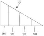
可选的,所述感应电极块的形状成为三角形或者梯形。Optionally, the shape of the sensing electrode block is a triangle or a trapezoid.
可选的,所述驱动电极和所述感应电极位于同一层,且各所述驱动电极部与各所述感应电极块之间相互间隔。Optionally, the driving electrodes and the sensing electrodes are located on the same layer, and each of the driving electrode parts and each of the sensing electrode blocks are spaced apart from each other.
可选的,所述驱动电极和所述感应电极均由金属网格膜层制作而成。Optionally, both the driving electrodes and the sensing electrodes are made of a metal mesh film layer.
可选的,相邻的两个所述驱动电极部的延伸方向呈第一角度,所述第一角度为锐角。Optionally, the extending directions of the two adjacent driving electrode parts are at a first angle, and the first angle is an acute angle.
可选的,相邻的两个所述驱动电极部中,其中一个驱动电极部的长度延伸方向为与所述第一方向垂直的第二方向,另一个驱动电极部的长度延伸方向与所述第二方向的夹角为所述第一角度。Optionally, in the two adjacent driving electrode parts, the length extending direction of one driving electrode part is a second direction perpendicular to the first direction, and the length extending direction of the other driving electrode part is the same as the length extending direction of the other driving electrode part. The included angle of the second direction is the first angle.
可选的,各所述驱动电极部为条形。Optionally, each of the driving electrode parts is strip-shaped.
可选的,还包括设置在所述衬底基板上的多条驱动电极引线和多条感应电极引线;Optionally, it also includes a plurality of driving electrode leads and a plurality of sensing electrode leads disposed on the base substrate;
每一行的所述驱动电极分别与对应的驱动电极引线连接,每一行的所述感应电极中的各所述感应电极块分别与对应的感应电极引线连接。The driving electrodes in each row are respectively connected with the corresponding driving electrode leads, and the sensing electrode blocks in the sensing electrodes in each row are respectively connected with the corresponding sensing electrode leads.
可选的,各所述驱动电极引线的接线端和各条所述感应电极引线的接线端均位于所述衬底基板的同一侧的周边非显示区域。Optionally, the terminals of each of the driving electrode leads and the terminals of each of the sensing electrode leads are located in the peripheral non-display area on the same side of the base substrate.
可选的,所述衬底基板与设置有触控电极图形一面相对的一面还设置有彩色滤光层。Optionally, a color filter layer is further provided on the side of the base substrate opposite to the side provided with the touch electrode pattern.
根据本发明实施例的第二方面,提供一种触控驱动方法,应用于上述任一项所述的触控基板,该驱动方法包括:According to a second aspect of the embodiments of the present invention, there is provided a touch driving method, which is applied to the touch substrate described in any one of the above, and the driving method includes:
向所述触控基板中的驱动电极施加驱动信号;applying a drive signal to the drive electrodes in the touch substrate;
检测发生触控前后的信号变化,以定位发生触控的位置,其中,所述信号变化为所述感应电极的感应电极块中被触控的感应电极区域与所述驱动电极之间的信号变化。根据本发明实施例的第三方面,提供一种触控显示面板,包括上述任一项所述的触控基板。Detecting the signal change before and after the touch occurs to locate the position where the touch occurs, wherein the signal change is the signal change between the touched sensing electrode area and the driving electrode in the sensing electrode block of the sensing electrode . According to a third aspect of the embodiments of the present invention, there is provided a touch display panel including the touch substrate described in any one of the above.
根据本发明实施例的第四方面,提供一种触控显示装置,包括上述所述的触控显示面板。According to a fourth aspect of the embodiments of the present invention, there is provided a touch display device including the above-mentioned touch display panel.
可选的,所述触控显示装置为键盘,所述键盘的主体上设置有所述触控显示面板,所述触控显示面板为条形,所述触控显示面板设置在所述主体的周边区域。Optionally, the touch display device is a keyboard, the main body of the keyboard is provided with the touch display panel, the touch display panel is strip-shaped, and the touch display panel is arranged on the main body. surrounding area.
根据上述实施例可知,该触控基板可进行多个触控位置的定位,实现多点触控,触控显示装置能够实现窄边框的设计。According to the above embodiments, the touch substrate can perform positioning of multiple touch positions to realize multi-point touch, and the touch display device can realize the design of a narrow frame.
应当理解的是,以上的一般描述和后文的细节描述仅是示例性和解释性的,并不能限制本发明。It is to be understood that both the foregoing general description and the following detailed description are exemplary and explanatory only and are not restrictive of the invention.
附图说明Description of drawings
此处的附图被并入说明书中并构成本说明书的一部分,示出了符合本发明的实施例,并与说明书一起用于解释本发明的原理。The accompanying drawings, which are incorporated in and constitute a part of this specification, illustrate embodiments consistent with the invention and together with the description serve to explain the principles of the invention.
图1是本发明一示例性实施例示出的触控基板的平面结构示意图;FIG. 1 is a schematic plan view of a touch substrate according to an exemplary embodiment of the present invention;
图2是本发明另一示例性实施例示出的触控基板的平面结构示意图;FIG. 2 is a schematic plan view of a touch substrate according to another exemplary embodiment of the present invention;
图3是本发明另一示例性实施例示出的感应电极块的平面结构示意图;3 is a schematic plan view of a sensing electrode block according to another exemplary embodiment of the present invention;
图4是本发明又一示例性实施例示出的触控基板的平面结构示意图;FIG. 4 is a schematic plan view of a touch substrate according to another exemplary embodiment of the present invention;
图5是本发明另一示例性实施例示出的触控基板的平面结构示意图;FIG. 5 is a schematic plan view of a touch substrate according to another exemplary embodiment of the present invention;
图6是本发明另一示例性实施例示出的触控显示面板的截面结构示意图;6 is a schematic cross-sectional structure diagram of a touch display panel according to another exemplary embodiment of the present invention;
图7是本发明另一示例性实施例示出的键盘的截面结构示意图;7 is a schematic cross-sectional structure diagram of a keyboard according to another exemplary embodiment of the present invention;
图8是相关技术一示例性实施例示出的触控基板的平面结构示意图;FIG. 8 is a schematic plan view of a touch substrate according to an exemplary embodiment of the related art;
图9是本发明另一示例性实施例示出的触控基板的平面结构示意图。FIG. 9 is a schematic plan view of a touch substrate according to another exemplary embodiment of the present invention.
具体实施方式Detailed ways
这里将详细地对示例性实施例进行说明,其示例表示在附图中。下面的描述涉及附图时,除非另有表示,不同附图中的相同数字表示相同或相似的要素。以下示例性实施例中所描述的实施方式并不代表与本发明相一致的所有实施方式。相反,它们仅是与如所附权利要求书中所详述的、本发明的一些方面相一致的装置和方法的例子。Exemplary embodiments will be described in detail herein, examples of which are illustrated in the accompanying drawings. Where the following description refers to the drawings, the same numerals in different drawings refer to the same or similar elements unless otherwise indicated. The implementations described in the illustrative examples below are not intended to represent all implementations consistent with the present invention. Rather, they are merely examples of apparatus and methods consistent with some aspects of the invention as recited in the appended claims.
本发明实施例提供了一种触控基板,包括:An embodiment of the present invention provides a touch substrate, including:
衬底基板,衬底基板上形成有触控电极图形;a base substrate, on which a touch electrode pattern is formed;
触控电极图形包括沿衬底基板的第一方向分布的至少一行绝缘设置的驱动电极和感应电极;The touch electrode pattern includes at least one row of drive electrodes and sensing electrodes distributed along the first direction of the base substrate and provided with insulation;
每一行的驱动电极具有多个相互连接的驱动电极部,感应电极包括多个感应电极块;The driving electrodes of each row have a plurality of interconnected driving electrode parts, and the sensing electrodes include a plurality of sensing electrode blocks;
各驱动电极部分别位于相邻的两个感应电极块之间;Each driving electrode part is respectively located between two adjacent sensing electrode blocks;
感应电极块具有多个面积不同的感应电极区域。The sensing electrode block has a plurality of sensing electrode regions with different areas.
衬底基板为具有触控电极图形的基板,该衬底基板可以为玻璃基板或其他适宜作为衬底的基板。The base substrate is a substrate with touch electrode patterns, and the base substrate can be a glass substrate or other suitable substrates.
该触控基板可以为显示面板中的彩膜基板或者阵列基板,或者单独实现触控功能的基板。The touch substrate may be a color filter substrate or an array substrate in a display panel, or a substrate that independently implements a touch function.
形成在衬底基板上的触控电极图形包括驱动电极和感应电极,驱动电极和感应电极之间相互绝缘,驱动电极和感应电极沿衬底基板的第一方向分布,衬底基板的第一方向可以为任意的一个方向,例如,可以为衬底基板的横向(例如,长度方向)或者纵向(例如,宽度方向),或者与衬底基板的横向呈一定角度的某一倾斜方向。The touch electrode pattern formed on the base substrate includes driving electrodes and sensing electrodes. The driving electrodes and sensing electrodes are insulated from each other. The driving electrodes and sensing electrodes are distributed along the first direction of the base substrate. It can be any one direction, for example, it can be the lateral direction (eg, the length direction) or the longitudinal direction (eg, the width direction) of the base substrate, or a certain inclined direction at a certain angle to the lateral direction of the base substrate.
衬底基板可以包括沿第一方向设置的一行或者多行驱动电极和感应电极,每一行的驱动电极均具有多个相互连接的驱动电极部,每个驱动电极部位于不同的位置,各驱动电极部之间可以通过连接线电连接,或者多个驱动电极部为一体形成的结构。The base substrate may include one or more rows of driving electrodes and sensing electrodes arranged along the first direction, each row of driving electrodes has a plurality of mutually connected driving electrode parts, each driving electrode part is located at a different position, and each driving electrode The parts can be electrically connected by connecting wires, or a structure in which a plurality of driving electrode parts are integrally formed.
每一行的感应电极均包括多个感应电极块,每个感应电极块为独立的感应电极块,每个感应电极块具有多个感应电极区域,每个感应电极区域的面积不同,并且,每个驱动电极部分别位于相邻的两个感应电极块之间,也即两个相邻的感应电极块之间夹设有驱动电极部。The sensing electrodes of each row include multiple sensing electrode blocks, each sensing electrode block is an independent sensing electrode block, each sensing electrode block has multiple sensing electrode areas, and the area of each sensing electrode area is different, and each sensing electrode block is different. The driving electrode parts are respectively located between two adjacent sensing electrode blocks, that is, the driving electrode parts are sandwiched between the two adjacent sensing electrode blocks.
当在驱动电极部施加驱动信号时,感应电极区域会与其相邻的驱动电极部之间形成电容以及形成对地电容,当某一区域被触控时,被触控区域对应的感应电极区域与驱动电极部之间的电容及对地电容会发生变化,可以检测到被触控区域的对应感应电极块中的感应电极区域的信号变化,由于感应电极块具有多个面积不同的感应电极区域,在发生触控前后不同的感应电极区域与驱动电极部之间的电容以及对地电容变化量,因此检测到的信号变化量也会不同,通过施加有信号的驱动电极所在行的位置可定位被触控区域在行方向的坐标,通过感应电极块中的感应电极区域的信号变化量可以定位出感应电极区域所在位置,即定位出被触控区域在该行上具体位置的坐标,即列方向上的坐标,据此可以定位触控位置,由于设置有多个感应电极块,每个感应电极块具有多个感应电极区域,因此,可进行多个触控位置的定位,实现多点触控。When a driving signal is applied to the driving electrode portion, the sensing electrode area will form a capacitance and a ground capacitance between the sensing electrode area and its adjacent driving electrode portion. When a certain area is touched, the sensing electrode area corresponding to the touched area will be the same as the The capacitance between the driving electrode parts and the capacitance to ground will change, and the signal change of the sensing electrode area in the corresponding sensing electrode block of the touched area can be detected. Since the sensing electrode block has multiple sensing electrode areas with different areas, Before and after the touch occurs, the capacitance between the sensing electrode area and the driving electrode part and the capacitance change to ground are different, so the detected signal change will also be different. The position of the row of the driving electrode to which the signal is applied can be located. The coordinates of the touch area in the row direction, the position of the sensing electrode area can be located by the signal variation of the sensing electrode area in the sensing electrode block, that is, the coordinates of the specific position of the touched area on the row, that is, the column direction According to the coordinates on the touch screen, the touch position can be located. Since there are multiple sensing electrode blocks, each sensing electrode block has multiple sensing electrode areas, so the positioning of multiple touch positions can be performed to realize multi-touch. .
上述的触控基板,通过一个感应电极块可进行多个触控位置的定位,每个感应电极块中的感应电极区域的数量和面积大小与所需的定位精度和能够检测到的信号变化量的灵敏度有关。For the above-mentioned touch substrate, multiple touch positions can be positioned through one sensing electrode block. The number and size of the sensing electrode areas in each sensing electrode block are related to the required positioning accuracy and the amount of signal variation that can be detected. related to the sensitivity.
图1为本发明一示例性实施例提供的触控基板的平面结构示意图,参照图1所示,该触控基板包括:FIG. 1 is a schematic plan view of a touch substrate provided by an exemplary embodiment of the present invention. Referring to FIG. 1 , the touch substrate includes:
衬底基板10,衬底基板10上形成有触控电极图形;A
触控电极图形包括沿衬底基板10的第一方向分布的多行驱动电极和感应电极,驱动电极和感应电极位于同一层;The touch electrode pattern includes multiple rows of driving electrodes and sensing electrodes distributed along the first direction of the
每一行的驱动电极具有多个相互连接的驱动电极部20,每一行的感应电极包括多个感应电极块30;The driving electrodes of each row have a plurality of driving
各驱动电极部20分别位于相邻的两个感应电极块30之间,且各驱动电极部20与各感应电极块30之间相互间隔;Each driving
感应电极块30具有多个面积不同的感应电极区域。The
图1中示意性的示出了5行沿第一方向分布的驱动电极和感应电极,在实际应用中可根据所需的触控基板的大小选用相应尺寸的衬底基板,根据需要和工艺设置驱动电极和触控电极的行数量。Figure 1 schematically shows five rows of driving electrodes and sensing electrodes distributed along the first direction. In practical applications, a substrate substrate of a corresponding size can be selected according to the required size of the touch substrate, and set according to needs and processes. The number of rows of drive electrodes and touch electrodes.
图1中第一方向为衬底基板的横向,例如图中双箭头线A所示方向,现有的触控电极图形通常沿横向在每一行只设置有驱动电极或者感应电极,沿衬底基板的纵向(与横向垂直的方向,例如图中双箭头线B所示方向)设置驱动电极和感应电极中的另一个;而本实施例中,沿衬底基板的横向,每一行均包括驱动电极和感应电极,并且,驱动电极和感应电极位于同一层。The first direction in FIG. 1 is the lateral direction of the base substrate, such as the direction indicated by the double arrow line A in the figure. The existing touch electrode patterns are usually provided with only driving electrodes or sensing electrodes in each row along the lateral direction. In the longitudinal direction (the direction perpendicular to the transverse direction, such as the direction indicated by the double arrow line B in the figure), the other one of the driving electrode and the sensing electrode is arranged; in this embodiment, along the transverse direction of the base substrate, each row includes a driving electrode and sensing electrodes, and the driving electrodes and sensing electrodes are located on the same layer.
如图1所示,每一行的驱动电极具有多个相互连接的驱动电极部20,每一行的感应电极包括多个感应电极块30,各驱动电极部20与各感应电极块30之间相互间隔,即驱动电极部20与感应电极块30之间间隔一定距离,使驱动电极部20与感应电极块30之间相互绝缘。As shown in FIG. 1 , the driving electrodes in each row have a plurality of driving
本实施例中,驱动电极和感应电极可采用相同的材料制作而成,通过将各驱动电极部与各感应电极块间隔一定距离,即可实现驱动电极与感应电极之间的相互绝缘,不需要设置绝缘层,驱动电极和感应电极可通过同一次构图工艺形成,因此,可减少触控电极图形的制备工艺步骤,节省制备材料,降低制备成本。In this embodiment, the driving electrodes and the sensing electrodes can be made of the same material. By separating each driving electrode part and each sensing electrode block by a certain distance, the mutual insulation between the driving electrodes and the sensing electrodes can be achieved, and there is no need to By disposing the insulating layer, the driving electrodes and the sensing electrodes can be formed through the same patterning process. Therefore, the preparation process steps of the touch electrode pattern can be reduced, the preparation materials can be saved, and the preparation cost can be reduced.
驱动电极和感应电极也可以位于不同的两层,驱动电极所在的层和触控电极所在的层之间可采用绝缘层进行绝缘。The driving electrodes and the sensing electrodes may also be located in two different layers, and an insulating layer may be used for insulation between the layer where the driving electrodes are located and the layer where the touch electrodes are located.
在一个可选的实施方式中,如图2所示,上述的驱动电极(具有多个驱动电极部20)和感应电极(具有多个感应电极块30)可采用金属网格膜层制作而成。In an optional embodiment, as shown in FIG. 2 , the above-mentioned driving electrodes (having a plurality of driving electrode parts 20 ) and sensing electrodes (having a plurality of sensing electrode blocks 30 ) can be made of a metal mesh film layer .
在采用触控基板制作具有触控功能的显示面板时,由于触控电极图形位于显示面板的图像显示区,为了使触控电极图形不影响图像的显示,触控电极图形需采用透明导电材料制作,透明导电材料例如为铟锡氧化物ITO(Indium tin oxide,简称ITO),ITO具有较好的导电性和透明性,但是ITO的电阻率较大,在采用其制作触控电极图形时,特别是应用在大尺寸的触控显示面板上时,容易造成驱动信号衰减和检测信号失真的问题,因此,影响触控位置定位的准确性。When using a touch substrate to make a display panel with touch function, since the touch electrode pattern is located in the image display area of the display panel, in order to prevent the touch electrode pattern from affecting the display of the image, the touch electrode pattern needs to be made of transparent conductive material. , The transparent conductive material is, for example, indium tin oxide ITO (Indium tin oxide, ITO for short). ITO has good conductivity and transparency, but the resistivity of ITO is relatively large. When using it to make touch electrode patterns, especially When applied to a large-sized touch display panel, it is easy to cause the problems of drive signal attenuation and detection signal distortion, thus affecting the accuracy of touch position positioning.
本实施例中,驱动电极和感应电极采用Metal mesh(金属网格)膜层制作而成,即驱动电极和感应电极的材料为导电金属材料,导电金属材料可采用电阻率低的金属,例如银或者铜等,导电金属材料的电阻率远小于ITO,因此可提高驱动电极和感应电极的导电性。In this embodiment, the driving electrodes and the sensing electrodes are made of Metal mesh (metal mesh) film layers, that is, the materials of the driving electrodes and the sensing electrodes are conductive metal materials, and the conductive metal materials can be metals with low resistivity, such as silver Or copper, etc., the resistivity of the conductive metal material is much smaller than that of ITO, so the conductivity of the driving electrode and the sensing electrode can be improved.
金属网格膜层指用导电金属材料制作的包括横纵交叉的多条金属线的膜层,金属线的线宽很小通常为微米级的,例如小于5微米,并且膜层厚度薄,对于肉眼是不可见的,网格的开口可透过光线,因此,金属网格膜层具有良好的导电性和透光性。The metal mesh film layer refers to a film layer made of conductive metal material including a plurality of metal lines crossing horizontally and vertically. It is invisible to the naked eye, and the openings of the grid can transmit light. Therefore, the metal grid film layer has good electrical conductivity and light transmission.
采用金属网格膜层制作驱动电极和感应电极,可减小驱动电极和感应电极的电阻率,提高触控位置的识别精度。Using the metal mesh film layer to make the driving electrodes and the sensing electrodes can reduce the resistivity of the driving electrodes and the sensing electrodes and improve the recognition accuracy of the touch position.
在一个可选的实施方式中,相邻的两个驱动电极部的延伸方向呈第一角度,第一角度为锐角。In an optional implementation manner, the extending directions of two adjacent driving electrode parts form a first angle, and the first angle is an acute angle.
参照图1所示,相邻的两个驱动电极部20,例如图中的第一驱动电极部21和第二驱动电极部22为相邻的两个驱动电极部,第一驱动电极部21的长度延伸方向和第二驱动电极部22的长度延伸方向的夹角为第一角度,该第一角度为锐角,可以根据经验设置。Referring to FIG. 1 , two adjacent driving
相邻的两个驱动电极部的长度延伸方向可以灵活设置,在一些例子中,参照图1所示,该两个驱动电极部,例如第一驱动电极部21的长度延伸方向为第二方向,该第二方向是与第一方向垂直的方向,第二驱动电极部22的长度延伸方向与第二方向的夹角为第一角度。The length extension directions of the two adjacent driving electrode parts can be set flexibly. In some examples, referring to FIG. 1 , the length extension direction of the two driving electrode parts, for example, the first
举例而言,驱动电极和感应电极沿衬底基板的横向分布,即第一方向为衬底基板的横向,第二方向为衬底基板的纵向,上述的第一驱动电极部21的长度延伸方向为纵向,即第一驱动电极部21沿衬底基板的纵向延伸,第二驱动电极部22的长度延伸方向为一倾斜方向,即第二驱动电极部22沿与纵向呈一定角度的方向延伸。For example, the driving electrodes and the sensing electrodes are distributed along the lateral direction of the base substrate, that is, the first direction is the lateral direction of the base substrate, the second direction is the longitudinal direction of the base substrate, and the above-mentioned lengthwise extending direction of the first
参照图1所示,上述的各驱动电极部20可以为条形,即驱动电极部20的长度方向大于宽度方向,该条形的驱动电极部20位于相邻的两个感应电极块30之间,上述相邻的第一驱动电极部21和第二驱动电极部22之间的夹角,即第一角度例如为锐角,该锐角的角度例如为30°至60°。Referring to FIG. 1 , each of the above-mentioned
需要说明书的是,图1中示出的驱动电极为一体形成的结构,驱动电极中设置在每两个感应电极块30之间的部分可分别作为一驱动电极部20,每个驱动电极部20位于不同的位置,从图1中可以看出,每个驱动电极部20分别位于相邻的两个感应电极块30之间,图1中驱动电极部30为条形,由相互连接的驱动电极部20组成的驱动电极为包括多个折弯的结构。It should be noted that the driving electrodes shown in FIG. 1 are integrally formed, and the part of the driving electrodes disposed between each two sensing electrode blocks 30 can be respectively used as a driving
在一个可选的实施方式中,参照图1所示,对于每一行的驱动电极和感应电极,各驱动电极部20的相对两侧分别设置有一感应电极块30。In an optional embodiment, as shown in FIG. 1 , for each row of driving electrodes and sensing electrodes, a
本实施例中,在每个驱动电极部20的相对两侧分别设置有一感应电极块30,例如,图1中第一驱动电极部21的左右两侧分别设置有一感应电极块30,第二驱动电极部22的上下两侧分别设置有一感应电极块30,每个驱动电极部20可分别与其相邻位置的两个感应电极块30形成电容,当发生触控时,可以增大被触控位置的感应电极块的感应电极区域的信号变化量,有利于提高触控位置的识别精度。In this embodiment, a
进一步的,位于驱动电极部其中一侧的所述感应电极块沿第一方向的宽度逐步增加;位于驱动电极部另一侧的感应电极块沿第一方向的宽度逐步减小。Further, the width of the sensing electrode blocks located on one side of the driving electrode portion along the first direction gradually increases; the width of the sensing electrode blocks located on the other side of the driving electrode portion gradually decreases along the first direction.
本实施例中,感应电极块的形状呈一定规律,第一方向例如为衬底基板的横向,参照图2所示,位于驱动电极部20的其中一侧的感应电极块30(称为第一感应电极块31)沿衬底基板10的横向其宽度逐步增加,即沿衬底基板10的横向,第一感应电极块31逐步变宽;位于驱动电极部20的另一侧的感应电极块30(称为第二感应电极块32)沿衬底基板10的横向的宽度逐步减小,即沿衬底基板10的横向,第二感应电极块32逐步变窄。In this embodiment, the shape of the sensing electrode block is regular, and the first direction is, for example, the lateral direction of the base substrate. Referring to FIG. 2 , the sensing electrode block 30 (called the first The width of the sensing electrode block 31) gradually increases along the lateral direction of the
由于感应电极块在第一方向的宽度不同,在第一方向上,可将感应电极块划分成多个部分,举例而言,感应电极块30为图3所示的三角形,可将该三角形的感应电极块30划分为若干个感应电极区域,例如图3所示,将感应电极块30划分为四个部分,每个部分为一个感应电极区域301,每个感应电极区域301的面积均不相同,由于每个感应电极区域301的面积均不相同,每个感应电极区域与驱动电极部之间的电容也不相同,在发生触控前后不同面积的感应电极区域与驱动电极部之间的电容以及对地电容变化量不同,据此检测到的信号变化量也会不同,因此,通过一个感应电极块可进行多个触控位置的定位。Since the widths of the sensing electrode blocks in the first direction are different, the sensing electrode blocks can be divided into multiple parts in the first direction. For example, the
本实施例中通过将感应电极块的形状呈一定规律,可使感应电极块具有不同面积的感应电极区域,并且感应电极块为一体设置的整体结构,对于感应电极块能够划分出的感应电极区域的数量与检测信号变化量的检测元件的灵敏度有关。In this embodiment, by making the shape of the sensing electrode blocks regular, the sensing electrode blocks can have sensing electrode areas of different areas, and the sensing electrode blocks are integrally arranged as a whole. The number is related to the sensitivity of the detection element that detects the amount of signal change.
通过实际实验数据表明,对于图2所示的触控电极图形排列方式,其中,驱动电极和感应电极采用金属网格膜层制作,感应电极块30为三角形,对于第一方向的边长L1为20mm,第二方向的边长L2为7mm的感应电极块30而言,当在驱动电极上施加驱动信号,同时检测各感应电极块上的信号变化,可以检测出每个感应电极块上四个不同区域的信号变化量,即每个感应电极块可具有四个感应电极区域,可分辨5mm*5mm的触控区域,其灵敏度与常规互容式电容触控面板相当。The actual experimental data shows that for the touch electrode pattern arrangement shown in FIG. 2 , the driving electrodes and the sensing electrodes are made of metal mesh film layers, the
上述的感应电极块30的形状例如为如图1所示三角形或者为如图4所示的梯形,感应电极块采用较为规则的图形,当驱动电极部20为图中所示的条形,且相邻的两个驱动电极部20的长度延伸方向呈第一角度,第一角度为锐角,其中,第一驱动电极部21沿第二方向延伸,第二驱动电极部22倾斜,驱动电极部20的相对两侧分别设置一感应电极块30,若位于两侧的感应电极块30的斜边与第一方向的边长的夹角为第一角度时,倾斜的第二驱动电极部22的上下两侧分别设置有两个感应电极块30,第一驱动电极块21的左右两侧分别设置有两个感应电极块30,这样,如图1和图4所示,两个感应电极块30可分别填补在倾斜方向的第二驱动电极部21的上下两侧,有效利用衬底基板上的有效面积,可整体提高触控电极图形在衬底基板上的占用率,提高对衬底基板的利用率。The shape of the above-mentioned
参照图5所示的本发明另一示例性实施例提供的触控基板,该触控基板中,衬底基板10上还设置有多条驱动电极引线41和多条感应电极引线42;每一行的驱动电极分别与对应的驱动电极引线41连接,每一行的感应电极中的各感应电极块30分别与对应的感应电极引线42连接。Referring to the touch substrate provided by another exemplary embodiment of the present invention shown in FIG. 5 , in the touch substrate, a plurality of driving electrode leads 41 and a plurality of sensing electrode leads 42 are further provided on the
由于每一行的驱动电极部相互连接形成驱动电极,因此,可将每一行的驱动电极的其中一侧边缘与一条驱动电极引线连接,或者是对于尺寸较大的衬底基板,可将每一行的驱动电极的两侧边缘分别与一条驱动电极引线连接,以通过两侧的驱动电极引线向驱动电极输入驱动信号,减小由于驱动电极电阻引线的信号衰减。Since the driving electrode parts of each row are connected to each other to form the driving electrodes, one side edge of the driving electrodes of each row can be connected to a driving electrode lead, or for the larger size of the substrate, the driving electrodes of each row can be connected to each other. The two sides of the driving electrode are respectively connected with a driving electrode lead, so as to input the driving signal to the driving electrode through the two sides of the driving electrode lead, and reduce the signal attenuation due to the resistance lead of the driving electrode.
由于每一行感应电极包括多个感应电极块,每个感应电极块分别与一条感应电极引线连接,通过感应电极引线传输对应感应电极块上的变化信号。Since each row of sensing electrodes includes a plurality of sensing electrode blocks, each sensing electrode block is respectively connected with a sensing electrode lead, and the change signal on the corresponding sensing electrode block is transmitted through the sensing electrode lead.
在将驱动电极部与驱动电极引线连接时,如图5所示的,驱动电极在两侧边缘可分别设置一独立的驱动电极部,两侧边缘的驱动电极部分别与一条驱动电极引线连接,或者也可以直接将驱动电极的两侧边缘均与对应的驱动电极引线连接。When connecting the driving electrode portion with the driving electrode lead, as shown in FIG. 5 , an independent driving electrode portion can be provided on the two edges of the driving electrode respectively, and the driving electrode portion on the two edges is respectively connected with a driving electrode lead. Alternatively, both side edges of the driving electrodes may be directly connected to the corresponding driving electrode leads.
本实施例中,设置有驱动电极引线和触控电极引线,驱动电极引线用于传输为驱动电极提供的驱动信号,触控电极引线用于传输触控电极输出的变化信号,该变化信号作为检测信号可传输给检测元件用于定位触控位置。In this embodiment, a drive electrode lead and a touch electrode lead are provided. The drive electrode lead is used to transmit the drive signal provided for the drive electrode, and the touch electrode lead is used to transmit the change signal output by the touch electrode, and the change signal is used as the detection signal. The signal can be transmitted to the detection element for locating the touch position.
对于包括多行驱动电极和感应电极的触控电极图形,可采用扫描的方式依次通过驱动电极引线向各行的驱动电极输入驱动信号,并采用扫描的方式依次输出通过感应电极引线输出的变化信号,据此实现对触控基板上被触控区域的位置定位。For touch electrode patterns including multiple rows of driving electrodes and sensing electrodes, the driving signals can be input to the driving electrodes of each row through the driving electrode leads in sequence by scanning, and the change signals output through the sensing electrode leads can be sequentially output by scanning. Accordingly, the position positioning of the touched area on the touch substrate is realized.
在一些例子中,各驱动电极引线的接线端和各条感应电极引线的接线端均位于衬底基板的同一侧的非显示周边区域。In some examples, the terminals of each of the driving electrode leads and the terminals of each of the sensing electrode leads are located in the non-display peripheral area on the same side of the base substrate.
参照图5所示,上述的各驱动电极引线41的接线端411和感应电极引线42的接线端421均位于衬底基板10的同一侧周边非显示区域。Referring to FIG. 5 , the
衬底基板的周边区域为非显示区域,接线端也可称为bonding pin,指用于将驱动电极引线与外部的驱动电路进行连接的端部,或者将感应电极引线与外部的检测元件进行连接的端部,将接线端均设置在同一侧的周边区域,例如图中所示的,接线端均位于衬底基板下方的周边区域,此种设置方式可以减小接线端占用的其他侧的周边区域的面积,有利于实现窄边框的触控基板。The peripheral area of the base substrate is a non-display area, and the terminal can also be called a bonding pin, which refers to the end used to connect the drive electrode lead with an external drive circuit, or connect the sensing electrode lead with an external detection element. The terminals are arranged in the peripheral area of the same side. For example, as shown in the figure, the terminals are located in the peripheral area below the substrate. This arrangement can reduce the peripheral area of the other side occupied by the terminals. The area of the area is favorable for realizing a touch substrate with a narrow frame.
在一些例子中,衬底基板与设置有触控电极图形的一面相对的一面还设置有彩色滤光层。In some examples, a color filter layer is further provided on the side of the base substrate opposite to the side provided with the touch electrode patterns.
衬底基板的其中一面(例如称为第一面)设置有触控电极图形,衬底基板的另一面(即与第一面相对的一面)设置有彩色滤光层,该触控基板可作为触控显示面板的彩膜基板,以形成On-cell触控显示面板。One side of the base substrate (for example, the first side) is provided with touch electrode patterns, and the other side of the base substrate (that is, the side opposite to the first side) is provided with a color filter layer. The touch substrate can be used as a The color filter substrate of the touch display panel is used to form an on-cell touch display panel.
彩色滤光层也可称为彩膜CF(Color filter,简称CF),彩色滤光层可以包括色阻层和黑矩阵层,黑矩阵层与色阻层相互间隔,色阻层可以包括红色(Red)色阻、绿色(Green)色阻和蓝色(Blue)色阻,各色阻之间通过黑矩阵层间隔;色阻层用于对光线进行过滤以显示彩色画面,黑矩阵层起到防止混色和漏光的作用。The color filter layer can also be called color filter CF (Color filter, CF for short). The color filter layer can include a color resist layer and a black matrix layer. Red) color resistance, green (Green) color resistance and blue (Blue) color resistance, each color resistance is separated by a black matrix layer; the color resistance layer is used to filter light to display color images, and the black matrix layer prevents The role of color mixing and light leakage.
本发明实施例还提供一种触控驱动方法,应用于上述任一实施例项所述的触控基板,该驱动方法包括:An embodiment of the present invention further provides a touch driving method, which is applied to the touch substrate described in any one of the above embodiments, and the driving method includes:
步骤S1、向触控基板中的驱动电极施加驱动信号;Step S1, applying a drive signal to the drive electrodes in the touch substrate;
步骤S2、检测发生触控前后的信号变化,以定位发生触控的位置,其中,所述信号变化为所述感应电极的感应电极块中被触控的感应电极区域与驱动电极之间的信号变化。Step S2: Detecting the signal change before and after the touch occurs to locate the position where the touch occurs, wherein the signal change is the signal between the touched sensing electrode area and the driving electrode in the sensing electrode block of the sensing electrode Variety.
该触控驱动方法在上述实施例中已经结合触控基板的结构进行描述,此处不再赘述。The touch driving method has been described in combination with the structure of the touch substrate in the above embodiments, and will not be repeated here.
本发明实施例还提供了一种触控显示面板,包括上述任一实施例所述逇触控基板。An embodiment of the present invention further provides a touch display panel, including the touch substrate described in any one of the above embodiments.
该触控显示面板可以为多种形式的电容触控屏,例如,OGS触控屏、On-cell触控屏和In-cell触控屏等。The touch display panel can be a capacitive touch screen in various forms, such as an OGS touch screen, an on-cell touch screen, an in-cell touch screen, and the like.
图6示出了一种On-cell触控显示面板的截面结构示意图,参照图6所示,该触控显示面板中的显示屏为液晶显示屏,对于液晶显示屏而言,其自下而上可以依次包括背光源100、阵列基板110、彩膜基板120和盖板130,阵列基板110和彩膜基板120之间设置有液晶层140,二者通过封框胶150粘合。FIG. 6 shows a schematic cross-sectional structure of an on-cell touch display panel. Referring to FIG. 6 , the display screen in the touch display panel is a liquid crystal display screen. The back
上述的彩膜基板120上远离阵列基板110的一面(即未设置彩色滤光层的一面)可设置有上述任一实施例所述的触控电极图形200,该彩膜基板120即为触控基板,并且在彩膜基板120上的触控电极图形200上还可以设置上偏光片160,然后在上偏光片160上进一步的设置盖板130,形成触控显示面板,该触控显示面板为On-cell触控屏。The above-mentioned
当然上述的触控显示面板中的显示屏也可以为其他形式的显示屏,例如有机发光二极管OLED(Organic Light Emitting Diode,简称OLED)显示屏或者为发光二极管LED(Light Emitting Diode,简称LED)显示屏等,本发明对此并不限定。Of course, the display screen in the above-mentioned touch display panel can also be other forms of display screen, such as organic light emitting diode OLED (Organic Light Emitting Diode, OLED for short) display or light emitting diode LED (Light Emitting Diode, LED for short) display screen, etc., which is not limited in the present invention.
本发明实施例还提供了一种触控显示装置,该触控显示装置包括上述的触控显示面板。An embodiment of the present invention further provides a touch display device, where the touch display device includes the above-mentioned touch display panel.
上述的触摸显示装置例如为键盘,所述键盘的主体上设置有上述实施例所述的触控显示面板,该触控显示面板为条形,该触控显示面板设置在主体的周边区域。The above-mentioned touch display device is, for example, a keyboard. The main body of the keyboard is provided with the touch display panel described in the above embodiments. The touch display panel is strip-shaped, and the touch display panel is arranged in the peripheral area of the main body.
本实施例提供的触控显示装置为键盘,在键盘的主体上设置有触控显示面板,设置触摸显示屏面板的区域可称为touch bar,该触控显示面板可作为设置键盘的触控按键,通过触控方式实现按键的功能,可以丰富键盘的按键功能,并且,可占用键盘的主体的较小空间内实现更多的按键功能,有利于键盘的轻薄化设计。The touch display device provided in this embodiment is a keyboard. A touch display panel is arranged on the main body of the keyboard. The area where the touch display panel is arranged can be called a touch bar, and the touch display panel can be used as a touch button for setting the keyboard. , the function of the keys is realized by the touch method, which can enrich the key functions of the keyboard, and can realize more key functions in a small space of the main body of the keyboard, which is beneficial to the thin and light design of the keyboard.
参照图7示出了的一种键盘的结构示意图,该键盘的主体300上设置有触摸显示面板400,主体300上设置有按一定规律排列的机械式按键310,图7中仅是示意性的示出了各机械式按键310,并不代表机械式按键310的实际排列方式,为了减小在主体300上设置触摸显示面板对现有按键排列布局设计变化,避免影响用户使用已有按键排列方式的习惯,将触控显示面板400设计为条形,并将其设置在主体300的周边区域,这样可不影响现有按键的排列方式。Referring to a schematic structural diagram of a keyboard shown in FIG. 7 , the
参照图8所示,为相关技术提供的在键盘上设置的触控显示面板中的触控基板上的触控电极的图形,该触控电极图形包括设置在衬底基板01上的驱动电极02和感应电极03,驱动电极02包括沿衬底基板的横向分布的一整块驱动电极块,感应电极03包括沿衬底基板的纵向延伸的多个感应电极块031,驱动电极02和感应电极03设置在两层,二者之间通过绝缘层绝缘。Referring to FIG. 8 , a pattern of touch electrodes on a touch substrate in a touch display panel provided on a keyboard provided for the related art, the touch electrode pattern includes driving
对于设置在键盘上的触控显示面板,如图8所述,在触控显示面板的触控基板中,沿衬底基板10的横向仅设置一行驱动电极02和感应电极03,衬底基板10上还设置有驱动电极线04和感应电极线05,将驱动电极02的两侧边分别与一条驱动电极线04连接,各感应电极块031分别与一条感应电极线05连接。For the touch display panel arranged on the keyboard, as shown in FIG. 8 , in the touch substrate of the touch display panel, only one row of driving
采用该结构触控电极图形的触控基板形成的触控显示面板,例如,显示区域尺寸约7mm*300mm,触控显示图形设置在显示区域,位于衬底基板01上侧的周边非显示区域和下侧的周边非显示区域的宽度L3例如为5mm,位于衬底基板左侧的周边非显示区域和右侧的周边非显示区域的宽度L4例如为2mm,每个触控电极块的触控区域的尺寸例如为5mm*5mm。For a touch display panel formed by using a touch substrate with a touch electrode pattern of this structure, for example, the size of the display area is about 7mm*300mm, the touch display pattern is arranged in the display area, and the peripheral non-display area on the upper side of the
对于上述尺寸的触控显示面板,约需要设置一个驱动电极和60个感应电极块,需要2条驱动电极引线和60条感应电极引线,并且还可以设置三条接地线,大约共需要65条电极引线,参照图8所示,驱动电极引线和感应电极引线均具有接线端,此处统一称为接线端,例如图中所示的接线端06,接线端也可称为bonding pin,若将接线端设置在衬底基板01的下侧周边区域,接线端需要占用的连接区域(可称为bonding区)长度至少为13mm,该长度远超出下侧周边区域的宽度L3,若将部分接线端放在左侧或者右侧周边区域,由于接线端本身的高度为1mm,也不足以放置多个接线端,因此采用上述的触控电极图形制作的触控显示面板,无法满足在键盘主体的剩余空间上设置的触控显示区域的要求。For the touch display panel of the above size, about one driving electrode and 60 sensing electrode blocks need to be set, 2 driving electrode leads and 60 sensing electrode leads are required, and three grounding lines can also be set, about a total of 65 electrode leads are required. 8, both the driving electrode lead and the sensing electrode lead have terminals, which are collectively referred to as terminals here, such as the terminal 06 shown in the figure, the terminal can also be called bonding pin. Set in the lower peripheral area of the
图9为本发明一示例性实施例提供的触控基板的平面结构示意图,该触控基板中,在衬底基板10的横向上分布有一行驱动电极和感应电极,该行的驱动电极具有多个相互连接的驱动电极部20,感应电极包括多个感应电极块30,驱动电极与一条驱动电极引线41连接,每个感应电极块30分别与一条感应电极引线42连接,驱动电极引线41的接线端411和各感应电极引线42的接线端421均位于衬底基板10的左侧周边非显示区域。9 is a schematic plan view of a touch substrate provided by an exemplary embodiment of the present invention. In the touch substrate, a row of driving electrodes and sensing electrodes are distributed in the lateral direction of the
对于采用上述结构的触控基板制作的触控显示面板,可将其设置在键盘上,在与上述相关技术中的触控显示面板具有相同的显示区域尺寸情况下,该触控显示基板中的驱动电极引线和触控电极引线的数量可控制在50根以内,可将驱动电极引线和触控电极引线的接线端设置在衬底基板的左侧或右侧周边区域,左侧或者右侧周边区域的宽度可以满足放置接线端的所需宽度,满足接线端占用的空间要求,因此,采用上述触控电极图形制造的触控显示面板,可满足在键盘的剩余空间内设置触控显示区域的要求。For the touch display panel made of the touch substrate with the above structure, it can be arranged on the keyboard. Under the condition that the touch display panel has the same display area size as the touch display panel in the above-mentioned related art, the touch display substrate in the touch display substrate has the same display area size. The number of driving electrode leads and touch electrode leads can be controlled within 50, and the terminals of the driving electrode leads and touch electrode leads can be arranged on the left or right peripheral area of the substrate, and the left or right peripheral area The width of the area can meet the required width for placing the terminals and the space occupied by the terminals. Therefore, the touch display panel manufactured with the above touch electrode pattern can meet the requirements of setting the touch display area in the remaining space of the keyboard. .
当然,上述的触控显示装置并不限于键盘,也可以其他类型的触控显示装置,例如,平板电脑、移动终端等。Of course, the above-mentioned touch display device is not limited to a keyboard, and other types of touch display devices, such as a tablet computer, a mobile terminal, etc., may also be used.
对于需要在一条形的区域设置触控显示面板的触控显示装置而言,其触控显示面板可以采用上述实施例所述的触控电极图形,以满足触控显示装置对设置触控显示面板的空间需求。For the touch display device that needs to set the touch display panel in a strip area, the touch display panel can use the touch electrode pattern described in the above embodiment, so as to satisfy the requirements of the touch display device for setting the touch display panel. space requirements.
本领域技术人员在考虑说明书及实践这里公开的公开后,将容易想到本发明的其它实施方案。本发明旨在涵盖本发明的任何变型、用途或者适应性变化,这些变型、用途或者适应性变化遵循本发明的一般性原理并包括本发明未公开的本技术领域中的公知常识或惯用技术手段。说明书和实施例仅被视为示例性的,本发明的真正范围和精神由下面的权利要求指出。Other embodiments of the invention will readily suggest themselves to those skilled in the art upon consideration of the specification and practice of the disclosure disclosed herein. The present invention is intended to cover any variations, uses or adaptations of the present invention which follow the general principles of the present invention and include common knowledge or conventional techniques in the technical field not disclosed by the present invention . The specification and examples are to be regarded as exemplary only, with the true scope and spirit of the invention being indicated by the following claims.
应当理解的是,本发明并不局限于上面已经描述并在附图中示出的精确结构,并且可以在不脱离其范围进行各种修改和改变。本发明的范围仅由所附的权利要求来限制。It should be understood that the present invention is not limited to the precise structures described above and illustrated in the accompanying drawings, and that various modifications and changes may be made without departing from the scope thereof. The scope of the present invention is limited only by the appended claims.
Claims (16)
Priority Applications (3)
| Application Number | Priority Date | Filing Date | Title |
|---|---|---|---|
| CN201810645537.1ACN108829297B (en) | 2018-06-21 | 2018-06-21 | Touch substrate, touch display panel, touch display device and touch driving method |
| US16/606,331US11237676B2 (en) | 2018-06-21 | 2019-03-22 | Touch substrate, touch display panel, touch display device and touch driving method |
| PCT/CN2019/079292WO2019242361A1 (en) | 2018-06-21 | 2019-03-22 | Touch substrate, touch display panel, touch display device and touch drive method |
Applications Claiming Priority (1)
| Application Number | Priority Date | Filing Date | Title |
|---|---|---|---|
| CN201810645537.1ACN108829297B (en) | 2018-06-21 | 2018-06-21 | Touch substrate, touch display panel, touch display device and touch driving method |
Publications (2)
| Publication Number | Publication Date |
|---|---|
| CN108829297A CN108829297A (en) | 2018-11-16 |
| CN108829297Btrue CN108829297B (en) | 2020-12-11 |
Family
ID=64141902
Family Applications (1)
| Application Number | Title | Priority Date | Filing Date |
|---|---|---|---|
| CN201810645537.1AExpired - Fee RelatedCN108829297B (en) | 2018-06-21 | 2018-06-21 | Touch substrate, touch display panel, touch display device and touch driving method |
Country Status (3)
| Country | Link |
|---|---|
| US (1) | US11237676B2 (en) |
| CN (1) | CN108829297B (en) |
| WO (1) | WO2019242361A1 (en) |
Families Citing this family (5)
| Publication number | Priority date | Publication date | Assignee | Title |
|---|---|---|---|---|
| CN108829297B (en)* | 2018-06-21 | 2020-12-11 | 京东方科技集团股份有限公司 | Touch substrate, touch display panel, touch display device and touch driving method |
| CN111142709B (en)* | 2019-12-27 | 2024-02-23 | 上海摩软通讯技术有限公司 | Touch panel and display device |
| CN211698920U (en)* | 2020-07-23 | 2020-10-16 | 深圳市汇顶科技股份有限公司 | Touch sensor, touch detection device, and electronic apparatus |
| US11327619B2 (en)* | 2020-09-22 | 2022-05-10 | Elo Touch Solutions, Inc. | Touchscreen device with non-orthogonal electrodes |
| US11558686B2 (en)* | 2020-12-02 | 2023-01-17 | Google Llc | Knob-like input for a hearable device |
Citations (1)
| Publication number | Priority date | Publication date | Assignee | Title |
|---|---|---|---|---|
| CN106249979A (en)* | 2016-08-31 | 2016-12-21 | 京东方科技集团股份有限公司 | Touch electrode structure and touch control display apparatus |
Family Cites Families (9)
| Publication number | Priority date | Publication date | Assignee | Title |
|---|---|---|---|---|
| JP5667960B2 (en)* | 2011-10-14 | 2015-02-12 | 株式会社ジャパンディスプレイ | Display device, touch detection device, and electronic device |
| JP6052914B2 (en)* | 2012-01-12 | 2016-12-27 | シナプティクス インコーポレイテッド | Single-layer capacitive imaging sensor |
| CN103268177B (en) | 2012-12-19 | 2016-09-07 | 上海天马微电子有限公司 | Capacitive touch module and touch display device |
| CN103279222B (en)* | 2013-05-24 | 2017-03-22 | 苏州欧菲光科技有限公司 | Touch panel and preparation method thereof |
| US9557361B2 (en)* | 2013-05-29 | 2017-01-31 | Atmel Corporation | Edgeless single-layer touch sensor |
| CN103677410A (en)* | 2013-12-02 | 2014-03-26 | 合肥京东方光电科技有限公司 | Touch base plate, touch screen and display device |
| TWM481451U (en)* | 2014-02-20 | 2014-07-01 | Hannstouch Solution Inc | Single layer solution touch panel |
| CN104238816A (en)* | 2014-09-04 | 2014-12-24 | 京东方科技集团股份有限公司 | Touch screen panel and manufacturing method thereof |
| CN108829297B (en) | 2018-06-21 | 2020-12-11 | 京东方科技集团股份有限公司 | Touch substrate, touch display panel, touch display device and touch driving method |
- 2018
- 2018-06-21CNCN201810645537.1Apatent/CN108829297B/ennot_activeExpired - Fee Related
- 2019
- 2019-03-22WOPCT/CN2019/079292patent/WO2019242361A1/ennot_activeCeased
- 2019-03-22USUS16/606,331patent/US11237676B2/enactiveActive
Patent Citations (1)
| Publication number | Priority date | Publication date | Assignee | Title |
|---|---|---|---|---|
| CN106249979A (en)* | 2016-08-31 | 2016-12-21 | 京东方科技集团股份有限公司 | Touch electrode structure and touch control display apparatus |
Also Published As
| Publication number | Publication date |
|---|---|
| US11237676B2 (en) | 2022-02-01 |
| WO2019242361A1 (en) | 2019-12-26 |
| CN108829297A (en) | 2018-11-16 |
| US20210223908A1 (en) | 2021-07-22 |
Similar Documents
| Publication | Publication Date | Title |
|---|---|---|
| CN108829297B (en) | Touch substrate, touch display panel, touch display device and touch driving method | |
| EP3101516B1 (en) | In cell touch panel and display device | |
| CN209248493U (en) | Function panel and terminal | |
| CN105224131B (en) | Array substrate, touch screen and touch control display apparatus | |
| US11188179B2 (en) | Touch panel and manufacturing method thereof, and touch display device | |
| CN105117075B (en) | A kind of smooth touch base plate, In-cell touch panel and display device | |
| JP5439565B2 (en) | Touch panel and manufacturing method thereof | |
| WO2020124770A1 (en) | Flexible touch-control display panel | |
| CN103995616B (en) | Embedded touch panel and display device | |
| CN104407758A (en) | Capacitive touch panel and display device | |
| CN204406362U (en) | Touch display device and touch substrate | |
| CN102207644A (en) | Color filter array substrate, liquid crystal display device comprising the same, and method for manufacturing the same | |
| KR20140004100A (en) | 3d touch control liquid crystal lens grating, method for manufacturing the same and 3d touch control display device | |
| CN204808294U (en) | Display panel and display device | |
| CN213904304U (en) | Touch substrate and display device | |
| CN102213852A (en) | Touch display device and manufacturing method thereof | |
| CN109491544B (en) | Touch display panel and display device | |
| CN108874222A (en) | Touch substrate, touch screen and touch device | |
| CN113867575B (en) | Touch display panel, display device and manufacturing method | |
| US20170235389A1 (en) | Touch Panel and Display Device | |
| CN204242157U (en) | Capacitive touch panel and display device | |
| TWM524954U (en) | Touch panel | |
| CN112527159A (en) | Touch substrate and display device | |
| CN110678831B (en) | Touch panel, touch substrate and touch display device | |
| CN105487701A (en) | Touch panel |
Legal Events
| Date | Code | Title | Description |
|---|---|---|---|
| PB01 | Publication | ||
| PB01 | Publication | ||
| SE01 | Entry into force of request for substantive examination | ||
| SE01 | Entry into force of request for substantive examination | ||
| GR01 | Patent grant | ||
| GR01 | Patent grant | ||
| CF01 | Termination of patent right due to non-payment of annual fee | ||
| CF01 | Termination of patent right due to non-payment of annual fee | Granted publication date:20201211 |