CN108807423B - Flexible electronic device and manufacturing method thereof, and flexible display device - Google Patents
Flexible electronic device and manufacturing method thereof, and flexible display deviceDownload PDFInfo
- Publication number
- CN108807423B CN108807423BCN201810608439.0ACN201810608439ACN108807423BCN 108807423 BCN108807423 BCN 108807423BCN 201810608439 ACN201810608439 ACN 201810608439ACN 108807423 BCN108807423 BCN 108807423B
- Authority
- CN
- China
- Prior art keywords
- flexible
- functional element
- protective layer
- rigid protective
- tft
- Prior art date
- Legal status (The legal status is an assumption and is not a legal conclusion. Google has not performed a legal analysis and makes no representation as to the accuracy of the status listed.)
- Active
Links
Images


Classifications
- H—ELECTRICITY
- H10—SEMICONDUCTOR DEVICES; ELECTRIC SOLID-STATE DEVICES NOT OTHERWISE PROVIDED FOR
- H10D—INORGANIC ELECTRIC SEMICONDUCTOR DEVICES
- H10D86/00—Integrated devices formed in or on insulating or conducting substrates, e.g. formed in silicon-on-insulator [SOI] substrates or on stainless steel or glass substrates
- H10D86/40—Integrated devices formed in or on insulating or conducting substrates, e.g. formed in silicon-on-insulator [SOI] substrates or on stainless steel or glass substrates characterised by multiple TFTs
- H10D86/411—Integrated devices formed in or on insulating or conducting substrates, e.g. formed in silicon-on-insulator [SOI] substrates or on stainless steel or glass substrates characterised by multiple TFTs characterised by materials, geometry or structure of the substrates
- G—PHYSICS
- G06—COMPUTING OR CALCULATING; COUNTING
- G06F—ELECTRIC DIGITAL DATA PROCESSING
- G06F1/00—Details not covered by groups G06F3/00 - G06F13/00 and G06F21/00
- G06F1/16—Constructional details or arrangements
- G06F1/1613—Constructional details or arrangements for portable computers
- G06F1/1633—Constructional details or arrangements of portable computers not specific to the type of enclosures covered by groups G06F1/1615 - G06F1/1626
- G06F1/1637—Details related to the display arrangement, including those related to the mounting of the display in the housing
- G06F1/1652—Details related to the display arrangement, including those related to the mounting of the display in the housing the display being flexible, e.g. mimicking a sheet of paper, or rollable
- G—PHYSICS
- G06—COMPUTING OR CALCULATING; COUNTING
- G06F—ELECTRIC DIGITAL DATA PROCESSING
- G06F1/00—Details not covered by groups G06F3/00 - G06F13/00 and G06F21/00
- G06F1/16—Constructional details or arrangements
- G06F1/18—Packaging or power distribution
- G06F1/189—Power distribution
- G—PHYSICS
- G09—EDUCATION; CRYPTOGRAPHY; DISPLAY; ADVERTISING; SEALS
- G09F—DISPLAYING; ADVERTISING; SIGNS; LABELS OR NAME-PLATES; SEALS
- G09F9/00—Indicating arrangements for variable information in which the information is built-up on a support by selection or combination of individual elements
- G09F9/30—Indicating arrangements for variable information in which the information is built-up on a support by selection or combination of individual elements in which the desired character or characters are formed by combining individual elements
- G09F9/301—Indicating arrangements for variable information in which the information is built-up on a support by selection or combination of individual elements in which the desired character or characters are formed by combining individual elements flexible foldable or roll-able electronic displays, e.g. thin LCD, OLED
- H—ELECTRICITY
- H10—SEMICONDUCTOR DEVICES; ELECTRIC SOLID-STATE DEVICES NOT OTHERWISE PROVIDED FOR
- H10D—INORGANIC ELECTRIC SEMICONDUCTOR DEVICES
- H10D86/00—Integrated devices formed in or on insulating or conducting substrates, e.g. formed in silicon-on-insulator [SOI] substrates or on stainless steel or glass substrates
- H10D86/01—Manufacture or treatment
- H10D86/021—Manufacture or treatment of multiple TFTs
- H—ELECTRICITY
- H10—SEMICONDUCTOR DEVICES; ELECTRIC SOLID-STATE DEVICES NOT OTHERWISE PROVIDED FOR
- H10D—INORGANIC ELECTRIC SEMICONDUCTOR DEVICES
- H10D86/00—Integrated devices formed in or on insulating or conducting substrates, e.g. formed in silicon-on-insulator [SOI] substrates or on stainless steel or glass substrates
- H10D86/40—Integrated devices formed in or on insulating or conducting substrates, e.g. formed in silicon-on-insulator [SOI] substrates or on stainless steel or glass substrates characterised by multiple TFTs
- H10D86/441—Interconnections, e.g. scanning lines
- H—ELECTRICITY
- H10—SEMICONDUCTOR DEVICES; ELECTRIC SOLID-STATE DEVICES NOT OTHERWISE PROVIDED FOR
- H10D—INORGANIC ELECTRIC SEMICONDUCTOR DEVICES
- H10D86/00—Integrated devices formed in or on insulating or conducting substrates, e.g. formed in silicon-on-insulator [SOI] substrates or on stainless steel or glass substrates
- H10D86/40—Integrated devices formed in or on insulating or conducting substrates, e.g. formed in silicon-on-insulator [SOI] substrates or on stainless steel or glass substrates characterised by multiple TFTs
- H10D86/60—Integrated devices formed in or on insulating or conducting substrates, e.g. formed in silicon-on-insulator [SOI] substrates or on stainless steel or glass substrates characterised by multiple TFTs wherein the TFTs are in active matrices
Landscapes
- Engineering & Computer Science (AREA)
- Theoretical Computer Science (AREA)
- Physics & Mathematics (AREA)
- General Physics & Mathematics (AREA)
- Computer Hardware Design (AREA)
- Human Computer Interaction (AREA)
- General Engineering & Computer Science (AREA)
- Power Engineering (AREA)
- Electroluminescent Light Sources (AREA)
- Devices For Indicating Variable Information By Combining Individual Elements (AREA)
Abstract
Translated fromChinese
Description
Translated fromChinese技术领域technical field
本发明涉及半导体技术领域,特别涉及一种柔性电子器件及其制造方法、柔性显示装置。The present invention relates to the technical field of semiconductors, and in particular, to a flexible electronic device, a manufacturing method thereof, and a flexible display device.
背景技术Background technique
柔性电子器件具有独特的延展性,且该柔性电子器件的制造成本较低,在信息、能源、医疗和国防等领域具有广泛应用前景。Flexible electronic devices have unique ductility and low manufacturing costs, and have broad application prospects in the fields of information, energy, medical care, and national defense.
柔性电子器件可以包括:多个阵列排布的刚性元件和多根柔性走线,每个刚性元件包括至少一个薄膜晶体管(英文:Thin-film transistor;简称:TFT),任意两个相邻的刚性元件中的TFT通过至少一根柔性走线连接。由于柔性电子器件在使用过程中会频繁弯折,为了避免损坏刚性元件中的TFT,可以在每个刚性元件的外部设置刚性保护层。The flexible electronic device may include: a plurality of rigid elements arranged in an array and a plurality of flexible wires, each rigid element includes at least one thin film transistor (English: Thin-film transistor; abbreviation: TFT), any two adjacent rigid elements The TFTs in the element are connected by at least one flexible trace. Since flexible electronic devices are frequently bent during use, in order to avoid damage to the TFTs in the rigid elements, a rigid protective layer can be provided outside each rigid element.
柔性电子器件中的柔性走线中被刚性保护层包裹的部分不易发生形变,而未被刚性保护层包裹的部分容易发生形变,该柔性走线中与刚性保护层的外表面接触的位置处的应力较为集中,导致该柔性走线中与刚性保护层的外表面接触的位置处的断线风险较大。The part of the flexible trace in the flexible electronic device that is wrapped by the rigid protective layer is not easily deformed, while the part not wrapped by the rigid protective layer is easily deformed. The stress is relatively concentrated, resulting in a greater risk of disconnection at the position of the flexible wiring that is in contact with the outer surface of the rigid protective layer.
发明内容SUMMARY OF THE INVENTION
本申请提供了一种柔性电子器件及其制造方法、柔性显示装置,可以解决现有的柔性走线中与刚性保护层的外表面接触的位置处的断线风险较大问题。所述技术方案如下:The present application provides a flexible electronic device, a method for manufacturing the same, and a flexible display device, which can solve the problem of high disconnection risk at the position contacting the outer surface of the rigid protective layer in the existing flexible wiring. The technical solution is as follows:
第一方面,提供了一种柔性电子器件,包括:In a first aspect, a flexible electronic device is provided, comprising:
柔性衬底基板;Flexible substrate substrate;
所述柔性衬底基板具有多个间隔设置的功能元件区,每个所述功能元件区中设置有至少一个TFT和包裹在所述至少一个TFT外部的刚性保护层;The flexible base substrate has a plurality of functional element regions arranged at intervals, each of the functional element regions is provided with at least one TFT and a rigid protective layer wrapped outside the at least one TFT;
所述柔性衬底基板上还设置有多根柔性走线,每个所述功能元件区中的TFT与另一个所述功能元件区中的TFT通过至少一根所述柔性走线连接;A plurality of flexible wirings are also arranged on the flexible substrate, and the TFT in each functional element region is connected to the TFT in another functional element region through at least one flexible wiring;
其中,每个所述功能元件区中设置的刚性保护层的中心区域的厚度大于边缘区域的厚度。Wherein, the thickness of the central region of the rigid protective layer disposed in each of the functional element regions is greater than the thickness of the edge region.
可选的,每个所述功能元件区中设置的刚性保护层的纵截面的形状为正梯形。Optionally, the shape of the longitudinal section of the rigid protective layer disposed in each of the functional element regions is a regular trapezoid.
可选的,每个所述功能元件区中设置的刚性保护层的纵截面的形状为弓形。Optionally, the shape of the longitudinal section of the rigid protective layer disposed in each of the functional element regions is arcuate.
可选的,每个所述功能元件区中设置的刚性保护层在所述柔性衬底基板上的正投影,与所述刚性保护层包裹的TFT所连接的柔性走线在所述柔性衬底基板上的正投影重叠。Optionally, the orthographic projection of the rigid protective layer disposed in each functional element area on the flexible substrate, the flexible wiring connected to the TFT wrapped by the rigid protective layer is on the flexible substrate. The orthographic projections on the substrate overlap.
可选的,每个所述功能元件区中设置的刚性保护层的材料包括橡胶或硅胶。Optionally, the material of the rigid protective layer provided in each of the functional element regions includes rubber or silicone.
可选的,所述柔性走线的材料包括金属材料或高分子导电材料。Optionally, the material of the flexible wiring includes metal material or polymer conductive material.
可选的,所述柔性电子器件为传感器,所述柔性走线的拉伸应变率小于或等于200%。Optionally, the flexible electronic device is a sensor, and the tensile strain rate of the flexible wire is less than or equal to 200%.
可选的,所述柔性电子器件为柔性显示基板,所述柔性走线的拉伸应变率小于或等于100%。Optionally, the flexible electronic device is a flexible display substrate, and the tensile strain rate of the flexible wiring is less than or equal to 100%.
第二方面,提供了一种柔性电子器件的制造方法,所述方法包括:In a second aspect, a method for manufacturing a flexible electronic device is provided, the method comprising:
在柔性衬底基板上形成多个TFT和多根柔性走线,其中,所述柔性衬底基板具有多个间隔设置的功能元件区,每个所述功能元件区中形成有至少一个TFT,每个所述功能元件区中的TFT与另一个所述功能元件区中的TFT通过至少一根所述柔性走线连接;A plurality of TFTs and a plurality of flexible wirings are formed on a flexible base substrate, wherein the flexible base substrate has a plurality of functional element regions arranged at intervals, and at least one TFT is formed in each of the functional element regions, and each functional element region is formed with at least one TFT. The TFTs in one of the functional element regions are connected to the TFTs in another functional element region through at least one of the flexible wires;
在每个所述功能元件区中形成包裹在所述至少一个TFT外部的刚性保护层,所述刚性保护层中心区域的厚度大于边缘区域的厚度。A rigid protective layer is formed in each of the functional element regions and wrapped around the outside of the at least one TFT, and the thickness of the central region of the rigid protective layer is greater than that of the edge region.
可选的,所述在每个所述功能元件区中形成包裹在所述至少一个TFT外部的刚性保护层,包括:Optionally, forming a rigid protective layer wrapped around the outside of the at least one TFT in each of the functional element regions includes:
采用灰度掩膜版对形成有所述多个TFT和所述多根柔性走线的柔性衬底基板进行表面张力改质处理,以使所述功能元件区中的中心区域的表面张力大于所述功能元件区中的边缘区域的表面张力,所述功能元件区中的边缘区域的表面张力大于所述柔性衬底基板中除所述多个功能元件区之外的区域的表面张力;A grayscale mask is used to perform surface tension modification treatment on the flexible base substrate formed with the plurality of TFTs and the plurality of flexible wirings, so that the surface tension of the central area in the functional element area is greater than that of all the surface tension of the edge region in the functional element region, the surface tension of the edge region in the functional element region is greater than the surface tension of the region other than the plurality of functional element regions in the flexible substrate substrate;
在表面张力改质处理后的柔性衬底基板上涂覆液态的刚性材料;Coating a liquid rigid material on the flexible substrate after surface tension modification;
固化所述液态的刚性材料以在每个所述功能元件区中形成所述刚性保护层。The liquid rigid material is cured to form the rigid protective layer in each of the functional element regions.
可选的,所述在每个所述功能元件区中形成包裹在所述至少一个TFT外部的刚性保护层,包括:Optionally, forming a rigid protective layer wrapped around the outside of the at least one TFT in each of the functional element regions includes:
在形成有所述多个TFT和所述多根柔性走线的柔性衬底基板上形成光刻胶薄膜;forming a photoresist film on the flexible base substrate on which the plurality of TFTs and the plurality of flexible wirings are formed;
采用灰度掩膜版对所述光刻胶薄膜进行曝光处理,并对曝光处理后的光刻胶薄膜进行显影处理,以在每个所述功能元件区中形成所述刚性保护层。The photoresist film is exposed to light using a grayscale mask, and the exposed photoresist film is developed to form the rigid protective layer in each of the functional element regions.
可选的,所述在柔性衬底基板上形成多个TFT和多根柔性走线之前,所述方法还包括:Optionally, before forming a plurality of TFTs and a plurality of flexible wires on the flexible substrate, the method further includes:
对所述柔性衬底基板进行表面硬度改质处理。Surface hardness modification treatment is performed on the flexible base substrate.
第三方面,提供了一种柔性显示装置,包括第一方面任一所述的柔性电子器件。In a third aspect, a flexible display device is provided, including the flexible electronic device according to any one of the first aspect.
本发明实施例提供的技术方案带来的有益效果至少包括:The beneficial effects brought by the technical solutions provided by the embodiments of the present invention include at least:
在柔性衬底基板的每个功能元件区设置至少一个TFT和包裹在该至少一个TFT外部的刚性保护层,每个功能元件区中的TFT与另一个功能元件区中的TFT通过至少一根柔性走线连接,每个功能元件区中的设置的刚性保护层的中心区域的厚度大于边缘区域的厚度。由于每个功能元件区中设置的刚性保护层中各位置处的硬度与对应位置处的厚度呈正相关,而该柔性电子器件中刚性保护层边缘区域的厚度较小,柔性走线中被刚性保护层包裹的部分的拉伸应变率,相对于相关技术中的柔性走线中被刚性保护层包裹的部分的拉伸应变率较大,避免了出现柔性走线中与刚性保护层的外表面接触的位置处的应力较为集中的现象,在刚性保护层能够对其包裹的TFT起到良好的保护作用的前提下,有效的降低了柔性走线中与刚性保护层的外表面接触的位置处的断线的概率。At least one TFT and a rigid protective layer wrapped around the outside of the at least one TFT are arranged in each functional element area of the flexible substrate substrate, and the TFT in each functional element area and the TFT in another functional element area pass through at least one flexible For wiring connections, the thickness of the central region of the rigid protective layer disposed in each functional element region is greater than the thickness of the edge region. Since the hardness at each position of the rigid protective layer set in each functional element area is positively correlated with the thickness at the corresponding position, and the thickness of the edge region of the rigid protective layer in the flexible electronic device is relatively small, the flexible wiring is rigidly protected by the rigid protective layer. The tensile strain rate of the part wrapped by the layer is larger than the tensile strain rate of the part wrapped by the rigid protective layer in the flexible trace in the related art, which avoids the occurrence of contact with the outer surface of the rigid protective layer in the flexible trace On the premise that the rigid protective layer can play a good protective effect on the wrapped TFT, the stress at the position of the flexible trace is relatively concentrated, effectively reducing the stress at the position where the flexible trace contacts the outer surface of the rigid protective layer. Probability of disconnection.
附图说明Description of drawings
为了更清楚地说明本发明实施例中的技术方案,下面将对实施例描述中所需要使用的附图作简单地介绍,显而易见地,下面描述中的附图仅仅是本发明的一些实施例,对于本领域普通技术人员来讲,在不付出创造性劳动的前提下,还可以根据这些附图获得其他的附图。In order to illustrate the technical solutions in the embodiments of the present invention more clearly, the following briefly introduces the accompanying drawings used in the description of the embodiments. Obviously, the accompanying drawings in the following description are only some embodiments of the present invention. For those of ordinary skill in the art, other drawings can also be obtained from these drawings without creative effort.
图1是相关技术提供的一种柔性电子器件的结构示意图;1 is a schematic structural diagram of a flexible electronic device provided by the related art;
图2是本发明实施例提供的一种柔性电子器件的结构示意图;2 is a schematic structural diagram of a flexible electronic device provided by an embodiment of the present invention;
图3是本发明实施例提供的另一种柔性电子器件的结构示意图;3 is a schematic structural diagram of another flexible electronic device provided by an embodiment of the present invention;
图4是本发明实施例提供的又一种柔性电子器件的结构示意图;4 is a schematic structural diagram of another flexible electronic device provided by an embodiment of the present invention;
图5是本发明实施例提供的一种柔性电子器件中柔性走线的发生形变的效果图;FIG. 5 is an effect diagram of deformation of a flexible wiring in a flexible electronic device provided by an embodiment of the present invention;
图6是本发明实施例提供的一种柔性电子器件的制造方法的流程图;6 is a flowchart of a method for manufacturing a flexible electronic device provided by an embodiment of the present invention;
图7是本发明实施例提供的另一种柔性电子器件的制造方法的流程图;7 is a flowchart of another method for manufacturing a flexible electronic device provided by an embodiment of the present invention;
图8是本发明实施例提供的一种对柔性衬底基板进行表面硬度改质处理后的效果图;8 is an effect diagram of a flexible substrate substrate after surface hardness modification treatment according to an embodiment of the present invention;
图9是本发明实施例提供的一种对形成有多个TFT和多根柔性走线的柔性衬底基板进行表面张力改质处理的示意图;9 is a schematic diagram of performing surface tension modification treatment on a flexible substrate substrate formed with a plurality of TFTs and a plurality of flexible wirings according to an embodiment of the present invention;
图10是本发明实施例提供的一种在表面张力改质处理后的柔性衬底基板上涂覆液态的刚性材料的示例图。FIG. 10 is an exemplary diagram of coating a liquid rigid material on a flexible substrate after surface tension modification treatment according to an embodiment of the present invention.
具体实施方式Detailed ways
为使本发明的目的、技术方案和优点更加清楚,下面将结合附图对本发明实施方式作进一步地详细描述。In order to make the objectives, technical solutions and advantages of the present invention clearer, the embodiments of the present invention will be further described in detail below with reference to the accompanying drawings.
请参考图1,图1是相关技术提供的一种柔性电子器件的结构示意图。该柔性电子器件可以包括:多个阵列排布的刚性元件01和多根柔性走线02。每个刚性元件01中包括至少一个TFT,任意两个相邻的刚性元件01中的TFT通过至少一根柔性走线02连接,每个刚性元件01的外部设置有刚性保护层03,通过该刚性保护层03可以对刚性元件01中的TFT进行保护。Please refer to FIG. 1 , which is a schematic structural diagram of a flexible electronic device provided by the related art. The flexible electronic device may include: a plurality of
由于柔性走线02被刚性保护层03包裹的部分不易发生形变(也即拉伸应变率较小,该拉伸应变率是指在外力拉伸的作用下,柔性走线的长度的变化率),而未被刚性保护层03包裹的部分容易发生形变(也即拉伸应变率较大),因此该柔性走线02中与刚性保护层03的外表面接触的位置处的应力较为集中,导致该柔性走线02中与刚性保护层03的外表面接触的位置处的断线风险较大。Because the part of the
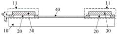
请参考图2,图2是本发明实施例提供的一种柔性电子器件的结构示意图,该柔性电子器件可以包括:Please refer to FIG. 2. FIG. 2 is a schematic structural diagram of a flexible electronic device provided by an embodiment of the present invention. The flexible electronic device may include:
柔性衬底基板10。
该柔性衬底基板10具有多个间隔设置的功能元件区11,每个功能元件区11中设置有至少一个TFT 20和包裹在该至少一个TFT 20外部的刚性保护层30。The
该柔性衬底基板10上还设置有多根柔性走线40,每个功能元件区11中的TFT 20与另一个功能元件区中的TFT 20通过至少一根柔性走线40连接。The
其中,每个功能元件区11中设置的刚性保护层30的中心区域的厚度d1大于边缘区域的厚度d2。参考图2可以看出,该刚性保护层30的厚度可以是指刚性保护层30远离柔性衬底基板10的一侧的表面与设置该TFT 20的承载面之间的距离。Wherein, the thickness d1 of the central region of the rigid
每个功能元件区11中设置的刚性保护层30中各位置处的硬度与对应位置处的厚度呈正相关,即刚性保护层30在某个位置处的厚度越厚,该位置处的硬度越大。由于每个功能元件区11中设置的至少一个TFT 20被刚性保护层30的中心区域包裹,该刚性保护层30的中心区域的厚度较大,因此该刚性保护层30的中心区域的硬度较大,该刚性保护层30能够对其包裹的TFT 20起到良好的保护作用。The hardness at each position of the rigid
又由于刚性保护层30边缘区域的厚度较小,刚性保护层30边缘区域的硬度较小,而刚性保护层30中各位置处的硬度与其包裹的柔性走线40在对应位置处的拉伸应变率呈负相关,因此柔性走线40中被刚性保护层包裹的部分的拉伸应变率,相对于相关技术中的柔性走线中被刚性保护层包裹的部分的拉伸应变率较大,避免了出现柔性走线40中与刚性保护层30的外表面接触的位置处的应力较为集中的现象,在刚性保护层30能够对其包裹的TFT 20起到良好的保护作用的前提下,有效的降低了柔性走线40中与刚性保护层30的外表面接触的位置处的断线的概率。In addition, due to the small thickness of the edge region of the rigid
综上所述,本发明实施例提供的柔性电子器件,在柔性衬底基板的每个功能元件区设置至少一个TFT和包裹在该至少一个TFT外部的刚性保护层,每个功能元件区中的TFT与另一个功能元件区中的TFT通过至少一根柔性走线连接,每个功能元件区中的设置的刚性保护层的中心区域的厚度大于边缘区域的厚度。由于每个功能元件区中设置的刚性保护层中各位置处的硬度与对应位置处的厚度呈正相关,而该柔性电子器件中刚性保护层边缘区域的厚度较小,柔性走线中被刚性保护层包裹的部分的拉伸应变率,相对于相关技术中的柔性走线中被刚性保护层包裹的部分的拉伸应变率较大,避免了出现柔性走线中与刚性保护层的外表面接触的位置处的应力较为集中的现象,在刚性保护层能够对其包裹的TFT起到良好的保护作用的前提下,有效的降低了柔性走线中与刚性保护层的外表面接触的位置处的断线的概率。To sum up, in the flexible electronic device provided by the embodiments of the present invention, at least one TFT and a rigid protective layer wrapped around the outside of the at least one TFT are arranged in each functional element area of the flexible substrate substrate, and the The TFT is connected to the TFT in another functional element region through at least one flexible wire, and the thickness of the central region of the rigid protective layer disposed in each functional element region is greater than that of the edge region. Since the hardness at each position of the rigid protective layer set in each functional element area is positively correlated with the thickness at the corresponding position, and the thickness of the edge region of the rigid protective layer in the flexible electronic device is relatively small, the flexible wiring is rigidly protected by the rigid protective layer. The tensile strain rate of the part wrapped by the layer is larger than the tensile strain rate of the part wrapped by the rigid protective layer in the flexible trace in the related art, which avoids the occurrence of contact with the outer surface of the rigid protective layer in the flexible trace On the premise that the rigid protective layer can play a good protective effect on the wrapped TFT, the stress at the position of the flexible trace is relatively concentrated, effectively reducing the stress at the position where the flexible trace contacts the outer surface of the rigid protective layer. Probability of disconnection.
在本发明实施例中,每个功能元件区上设置的刚性保护层的形状有多种,本发明实施例以以下两种可现实方式为例进行示意性说明:In the embodiment of the present invention, there are various shapes of the rigid protective layer provided on each functional element area. The embodiment of the present invention takes the following two practical ways as examples for schematic illustration:
在第一种可实现方式中,请参考图3,图3是本发明实施例提供的另一种柔性电子器件的结构示意图,每个功能元件区11中设置的刚性保护层30的纵截面的形状为正梯形,该纵截面垂直于柔性衬底基板10的承载面。在该承载面上可以设置TFT 20、刚性保护层30和柔性走线40。需要说明的是,由于该刚性保护层20在包裹TFT 20,图3示出的刚性保护层30的纵截面的形状是从某一个方向上所截到的图形,因此图3中的刚性保护层的形状并不是正梯形,实际应用中,该刚性保护层20在包裹TFT 20后的整体形状是正梯形。In the first possible implementation, please refer to FIG. 3 . FIG. 3 is a schematic structural diagram of another flexible electronic device provided by an embodiment of the present invention. The longitudinal section of the rigid
在第二种可实现方式中,请参考图4,图4是本发明实施例提供的又一种柔性电子器件的结构示意图,每个功能元件区11中设置的刚性保护层30的纵截面的形状为弓形,该纵截面垂直于柔性衬底基板10的承载面。需要说明的是,由于该刚性保护层20在包裹TFT20,图4示出的刚性保护层30的纵截面的形状是从某一个方向上所截到的图形,因此图4中的刚性保护层的形状并不是弓形,实际应用中,该刚性保护层20在包裹TFT 20后的整体形状是弓形。In the second implementation manner, please refer to FIG. 4 . FIG. 4 is a schematic structural diagram of another flexible electronic device provided by an embodiment of the present invention. The longitudinal section of the rigid
如图3和图4所示,每个功能元件区11中设置的刚性保护层30中从中心区域到边缘区域的厚度逐渐减小,在柔性走线40中,其与TFT 20连接的位置a的拉伸应变率最小,保证了TFT 20与柔性走线40之间能够有效的连接;该柔性走线40与刚性保护层30的外表面接触的位置b处的拉伸应变率最大,保证了柔性走线40能够充分的被拉伸;该柔性走线40中从位置a到位置b处的拉伸应变率是逐渐变大的,避免了柔性走线40中某个位置处的拉伸应变率发生突变,导致该位置处的拉伸应变率发生突变,在该位置处的容易出现断裂的现象,进一步的降低了柔性走线40发生断线的概率。As shown in FIG. 3 and FIG. 4 , the thickness of the rigid
在本发明实施例中,如图3或图4所示,每个功能元件区11中设置的刚性保护层30在柔性衬底基板10上的正投影,与刚性保护层30包裹的TFT 20所连接的柔性走线30在柔性衬底基板10上的正投影重叠。In the embodiment of the present invention, as shown in FIG. 3 or FIG. 4 , the orthographic projection of the rigid
可选的,在该柔性电子器件使用过程中,为了保证每个功能元件区11中设置的刚性保护层30能够有效的对其包裹的TFT 20起到保护作用,该刚性保护层30的中心区域的厚度d1可以满足:0.5≤d1≤5微米(um)。为了保证柔性走线40能够充分的被拉伸,每个功能元件区11中设置的刚性保护层30的边缘区域的厚度d2可以满足:0.3≤d2≤0.9um。在一种可选的实现方式中,该边缘区域的厚度d2稍微大于柔性走线40的厚度即可。Optionally, during the use of the flexible electronic device, in order to ensure that the rigid
可选的,每个功能元件区11中设置的刚性保护层30的材料可以包括橡胶或硅胶。柔性走线40的材料可以包括金属材料或高分子导电材料,例如,该金属材料可以包括金属铝、金属银或合金材料等;该高分子导电材料可以包括聚乙炔、聚吡咯、聚对苯撑、聚苯硫醚或聚苯胺等。Optionally, the material of the rigid
在本发明实施例中,请参考图5,图5是本发明实施例提供的一种柔性电子器件中柔性走线的发生形变的效果图,柔性电子器件中的柔性走线40的拉伸应变率满足以下计算公式:In the embodiment of the present invention, please refer to FIG. 5 . FIG. 5 is an effect diagram of the deformation of a flexible wire in a flexible electronic device provided by an embodiment of the present invention, and the tensile strain of the

其中,δ为柔性走线40的拉伸应变率;L1为该柔性走线40未被拉伸时,该柔性走线40所连接的TFT对应的两个刚性保护层30之间的距离;L2为柔性走线40被拉伸后,该柔性走线40所连接的TFT对应的两个刚性保护层30之间的距离。Wherein, δ is the tensile strain rate of the
在一种可选的实现方式中,该柔性电子器件可以为传感器或柔性显示基板等,该柔性电子器件的用途不同,该柔性电子器件中柔性走线40的拉伸应变率也不同。In an optional implementation manner, the flexible electronic device may be a sensor or a flexible display substrate, and the like. The purpose of the flexible electronic device is different, and the tensile strain rate of the
示例的,当柔性电子器件为传感器时,该柔性电子器件可以设置在显示装置中,对显示装置的温度或亮度等进行检测;该柔性电子器件还可以贴附在人体的皮肤上,对人体的体温或心率等进行检测,为了避免柔性走线40被拉断,柔性走线40的拉伸应变率小于或等于200%。For example, when the flexible electronic device is a sensor, the flexible electronic device can be arranged in the display device to detect the temperature or brightness of the display device; the flexible electronic device can also be attached to the skin of the human body, so that the Body temperature or heart rate are detected. In order to prevent the
当柔性电子器件为柔性显示基板时,该柔性电子器件可以设置在显示装置中,该柔性电子器件中每个功能区为一个像素,为了保证显示装置的显示质量,需要避免柔性走线30的拉伸应变率过大,通常该柔性走线40的拉伸应变率小于或等于100%。When the flexible electronic device is a flexible display substrate, the flexible electronic device can be arranged in the display device, and each functional area in the flexible electronic device is a pixel. In order to ensure the display quality of the display device, it is necessary to avoid pulling the
综上所述,本发明实施例提供的柔性电子器件,在柔性衬底基板的每个功能元件区设置至少一个TFT和包裹在该至少一个TFT外部的刚性保护层,每个功能元件区中的TFT与另一个功能元件区中的TFT通过至少一根柔性走线连接,每个功能元件区中的设置的刚性保护层的中心区域的厚度大于边缘区域的厚度。由于每个功能元件区中设置的刚性保护层中各位置处的硬度与对应位置处的厚度呈正相关,而该柔性电子器件中刚性保护层边缘区域的厚度较小,柔性走线中被刚性保护层包裹的部分的拉伸应变率,相对于相关技术中的柔性走线中被刚性保护层包裹的部分的拉伸应变率较大,避免了出现柔性走线中与刚性保护层的外表面接触的位置处的应力较为集中的现象,在刚性保护层能够对其包裹的TFT起到良好的保护作用的前提下,有效的降低了柔性走线中与刚性保护层的外表面接触的位置处的断线的概率。To sum up, in the flexible electronic device provided by the embodiments of the present invention, at least one TFT and a rigid protective layer wrapped around the outside of the at least one TFT are arranged in each functional element area of the flexible substrate substrate, and the The TFT is connected to the TFT in another functional element region through at least one flexible wire, and the thickness of the central region of the rigid protective layer disposed in each functional element region is greater than that of the edge region. Since the hardness at each position of the rigid protective layer set in each functional element area is positively correlated with the thickness at the corresponding position, and the thickness of the edge region of the rigid protective layer in the flexible electronic device is relatively small, the flexible wiring is rigidly protected by the rigid protective layer. The tensile strain rate of the part wrapped by the layer is larger than the tensile strain rate of the part wrapped by the rigid protective layer in the flexible trace in the related art, which avoids the occurrence of contact with the outer surface of the rigid protective layer in the flexible trace On the premise that the rigid protective layer can play a good protective effect on the wrapped TFT, the stress at the position of the flexible trace is relatively concentrated, effectively reducing the stress at the position where the flexible trace contacts the outer surface of the rigid protective layer. Probability of disconnection.
请参考图6,图6是本发明实施例提供的一种柔性电子器件的制造方法的流程图,该方法用于制造图2示出的柔性电子器件,该方法可以包括:Please refer to FIG. 6. FIG. 6 is a flowchart of a method for manufacturing a flexible electronic device provided by an embodiment of the present invention. The method is used to manufacture the flexible electronic device shown in FIG. 2. The method may include:
步骤601、在柔性衬底基板上形成多个TFT和多根柔性走线。
其中,柔性衬底基板具有多个间隔设置的功能元件区,每个功能元件区中形成有至少一个TFT,每个功能元件区中的TFT与另一个功能元件区中的TFT通过至少一根柔性走线连接。Wherein, the flexible substrate has a plurality of functional element regions arranged at intervals, each functional element region is formed with at least one TFT, and the TFT in each functional element region and the TFT in another functional element region pass through at least one flexible wire connection.
步骤602、在每个功能元件区中形成包裹在至少一个TFT外部的刚性保护层。
其中,该刚性保护层中心区域的厚度大于边缘区域的厚度。Wherein, the thickness of the central region of the rigid protective layer is greater than the thickness of the edge region.
综上所述,本发明实施例提供的柔性电子器件的制造方法,在柔性衬底基板的每个功能元件区形成至少一个TFT和包裹在该至少一个TFT外部的刚性保护层,每个功能元件区中的TFT与另一个功能元件区中的TFT通过至少一根柔性走线连接,每个功能元件区中的形成的刚性保护层的中心区域的厚度大于边缘区域的厚度。由于每个功能元件区中形成的刚性保护层中各位置处的硬度与对应位置处的厚度呈正相关,而该柔性电子器件中刚性保护层边缘区域的厚度较小,柔性走线中被刚性保护层包裹的部分的拉伸应变率,相对于相关技术中的柔性走线中被刚性保护层包裹的部分的拉伸应变率较大,避免了出现柔性走线中与刚性保护层的外表面接触的位置处的应力较为集中的现象,在刚性保护层能够对其包裹的TFT起到良好的保护作用的前提下,有效的降低了柔性走线中与刚性保护层的外表面接触的位置处的断线的概率。To sum up, in the method for manufacturing a flexible electronic device provided by the embodiment of the present invention, at least one TFT and a rigid protective layer wrapped around the outside of the at least one TFT are formed in each functional element area of the flexible substrate, and each functional element The TFTs in the region are connected to the TFTs in another functional element region through at least one flexible wire, and the thickness of the central region of the rigid protective layer formed in each functional element region is greater than that of the edge region. Since the hardness at each position of the rigid protection layer formed in each functional element area is positively correlated with the thickness at the corresponding position, and the thickness of the edge region of the rigid protection layer in the flexible electronic device is relatively small, the flexible trace is rigidly protected by rigid protection. The tensile strain rate of the part wrapped by the layer is larger than the tensile strain rate of the part wrapped by the rigid protective layer in the flexible trace in the related art, which avoids the occurrence of contact with the outer surface of the rigid protective layer in the flexible trace On the premise that the rigid protective layer can play a good protective effect on the wrapped TFT, the stress at the position of the flexible trace is relatively concentrated, effectively reducing the stress at the position where the flexible trace contacts the outer surface of the rigid protective layer. Probability of disconnection.
请参考图7,图7是本发明实施例提供的另一种柔性电子器件的制造方法的流程图,该方法用于制造图2、图3或图4示出的柔性电子器件,该方法可以包括:Please refer to FIG. 7 . FIG. 7 is a flowchart of another method for manufacturing a flexible electronic device provided by an embodiment of the present invention. The method is used to manufacture the flexible electronic device shown in FIG. 2 , FIG. 3 or FIG. 4 . The method may include:
步骤701、对柔性衬底基板进行表面硬度改质处理。
在本发明实施例中,为了提高柔性电子器件的性能,需要将该柔性电子器件中的柔性衬底基板进行硬度改质处理,使得柔性衬底基板中功能元件区对应的硬度大于柔性衬底基板除功能元件区之外的区域对应的硬度。In the embodiment of the present invention, in order to improve the performance of the flexible electronic device, it is necessary to perform hardness modification treatment on the flexible substrate substrate in the flexible electronic device, so that the hardness corresponding to the functional element area in the flexible substrate substrate is greater than that of the flexible substrate substrate The hardness corresponding to the area other than the functional element area.
示例的,如图8所示,图8是本发明实施例提供的一种对柔性衬底基板进行表面硬度改质处理后的效果图,可以对柔性衬底基板10的进行图形化处理,使得柔性衬底基板10上形成多个凸台结构12,该凸台结构12所在的区域的硬度大于除凸台结构12所在区域之外的区域的硬度,该凸台结构12所在的区域即为功能元件区11,该图形化处理可以包括:光刻胶涂覆、曝光、显影、刻蚀和光刻胶剥离。As an example, as shown in FIG. 8 , FIG. 8 is an effect diagram of a flexible substrate substrate after surface hardness modification treatment provided by an embodiment of the present invention. The
步骤702、在硬度改质处理后的柔性衬底基板上形成多个TFT和多根柔性走线。
其中,每个功能元件区中(也即每个凸台结构上)形成至少一个TFT,每个功能元件区中的TFT与另一个功能元件区中的TFT通过至少一根柔性走线连接。Wherein, at least one TFT is formed in each functional element region (ie, on each boss structure), and the TFT in each functional element region is connected to the TFT in another functional element region through at least one flexible wire.
在本发明实施例中,在对柔性衬底基板进行表面硬度改质处理后,可以直接形成多个TFT和多根柔性走线,也可以通过转印的方式在硬度改质处理后的柔性衬底基板上形成多个TFT和多根柔性走线。In the embodiment of the present invention, after the surface hardness modification treatment is performed on the flexible substrate, a plurality of TFTs and a plurality of flexible wirings can be directly formed, or the flexible substrate after the hardness modification treatment can be transferred by means of transfer printing. A plurality of TFTs and a plurality of flexible wirings are formed on the base substrate.
示例的,当需要通过转印的方式在柔性衬底基板上形成多个TFT和多根柔性走线时,可以先在另一个衬底基板上形成多个TFT和多根柔性走线;再将硬度改质处理后的柔性衬底基板进行预应变处理,该预应变处理是指将柔性衬底基板沿长度方向和宽度方向各拉伸一定的距离;然后将衬底基板上形成的多个TFT和多根柔性走线转印到具有预应变的柔性衬底基板上,该TFT需要形成在功能元件区中;最后释放对柔性衬底基板施加的预应变,从而在柔性衬底基板上形成多个TFT和多根柔性走线。通过转印的方式在柔性衬底基板上形成多个TFT和多根柔性走线,可以增大柔性走线的拉伸应变率,使得后续形成的柔性电子器件的拉伸效果较好。For example, when multiple TFTs and multiple flexible wirings need to be formed on a flexible substrate by transfer printing, multiple TFTs and multiple flexible wirings can be formed on another substrate first; The flexible substrate after the hardness modification treatment is subjected to pre-strain treatment. The pre-strain treatment refers to stretching the flexible substrate by a certain distance along the length direction and the width direction; and a plurality of flexible traces are transferred to the flexible substrate with pre-strain, the TFT needs to be formed in the functional element area; finally, the pre-strain applied to the flexible substrate is released, so as to form multiple flexible substrates on the flexible substrate. TFT and multiple flexible traces. By forming a plurality of TFTs and a plurality of flexible wirings on the flexible substrate by means of transfer printing, the tensile strain rate of the flexible wirings can be increased, so that the subsequently formed flexible electronic device has a better tensile effect.
步骤703、在每个功能元件区中形成包裹在至少一个TFT外部的刚性保护层。
在本发明实施例中,在每个功能元件区中形成包裹在至少一个TFT外部的刚性保护层有多种可实现方式,本发明实施例以以下两种可实现方式为例进行示意性说明:In the embodiment of the present invention, there are multiple implementations for forming a rigid protective layer wrapped outside at least one TFT in each functional element region. The embodiment of the present invention takes the following two implementations as examples for schematic illustration:
在第一种可实现方式中,在每个功能元件区中形成包裹在至少一个TFT外部的刚性保护层,可以包括如下几个步骤:In a first implementation manner, forming a rigid protective layer wrapped around at least one TFT in each functional element region may include the following steps:
步骤A1、采用灰度掩膜版对形成有多个TFT和多根柔性走线的柔性衬底基板进行表面张力改质处理,以使功能元件区中的中心区域的表面张力大于功能元件区中的边缘区域的表面张力,功能元件区中的边缘区域的表面张力大于柔性衬底基板中除多个功能元件区之外的区域的表面张力。Step A1, using a grayscale mask to perform surface tension modification treatment on the flexible substrate formed with multiple TFTs and multiple flexible wirings, so that the surface tension of the central area in the functional element area is greater than that in the functional element area The surface tension of the edge region of the functional element region is greater than the surface tension of the region except the plurality of functional element regions in the flexible substrate substrate.
示例的,请参考图9,图9是本发明实施例提供的一种对形成有多个TFT和多根柔性走线的柔性衬底基板进行表面张力改质处理的示意图,可以采用该灰度掩膜版00对柔性衬底基板进行表面张力改质处理,该灰度掩膜版00可以包括:非透光区域001、半透光区域002和透光区域003。其中,非透光区域001的透光率大于半透光区域002的透光率,半透光区域002的透光率大于透光区域003的透光率。该非透光区域001对应功能元件区11中的中心区域,半透光区域002可以对应功能元件区11中的边缘区域,透光区域003可以对应柔性衬底基板10中除多个功能元件区11之外的区域。在紫外线经过该灰度掩膜版00照射在柔性衬底基板11上时,由于掩膜版各区域的透光率不同,柔性衬底基板中对应区域的经过不同光强的紫外线后,柔性衬底基板中各区域的亲疏水性也发生了变化,而柔性衬底基板的亲疏水性与表面张力相关,因此在紫外线经过该灰度掩膜版00照射在柔性衬底基板10后,柔性衬底基板10上的功能元件区11中的中心区域的表面张力大于功能元件区11中的边缘区域的表面张力,功能元件区中的边缘区域11的表面张力大于柔性衬底基板10中除多个功能元件区11之外的区域的表面张力。For example, please refer to FIG. 9 , which is a schematic diagram of performing surface tension modification treatment on a flexible substrate formed with a plurality of TFTs and a plurality of flexible wirings according to an embodiment of the present invention. This grayscale can be used. The
步骤B1、在表面张力改质处理后的柔性衬底基板上涂覆液态的刚性材料。Step B1, coating a liquid rigid material on the surface tension modified flexible substrate.
可选的,该液态的刚性材料可以包括橡胶材料或硅胶材料。Optionally, the liquid rigid material may include rubber material or silicone material.
在本发明实施例中,请参考图10,图10是本发明实施例提供的一种在表面张力改质处理后的柔性衬底基板上涂覆液态的刚性材料的示例图,在对柔性衬底基板10进行表面张力处理后,可以在该柔性衬底基板10上涂覆液态的刚性材料50。In an embodiment of the present invention, please refer to FIG. 10 . FIG. 10 is an exemplary diagram of coating a liquid rigid material on a flexible substrate after surface tension modification treatment provided by an embodiment of the present invention. After the
由于液态的刚性材料在柔性衬底基板的表面上的厚度与衬底基板的表面张力呈正相关,该柔性衬底基板中各区域的表面张力不同,在该柔性衬底基板上入涂覆液态的刚性材料后,因此,该柔性衬底基板中表面张力较大的区域中形成的液态的刚性材料的厚度较大,柔性衬底基板中表面张力较小的区域中形成的液态的刚性材料的厚度较小。需要说明书的是,对柔性衬底基板进行表面张力改质处理时,需要保证液态的刚性材料不能形成在柔性衬底基板中除功能元件区之外的区域中。Since the thickness of the liquid rigid material on the surface of the flexible substrate is positively correlated with the surface tension of the substrate, the surface tension of each region in the flexible substrate is different. After the rigid material, therefore, the thickness of the liquid rigid material formed in the area with a larger surface tension in the flexible substrate substrate is larger, and the thickness of the liquid rigid material formed in the area with a smaller surface tension in the flexible substrate substrate smaller. It should be noted that, when the surface tension modification treatment is performed on the flexible substrate, it is necessary to ensure that the liquid rigid material cannot be formed in the area of the flexible substrate other than the functional element area.
步骤C1、固化液态的刚性材料以在每个功能元件区中形成刚性保护层。Step C1, curing the liquid rigid material to form a rigid protective layer in each functional element area.
在本发明实施例中,固化液态的刚性材料后,可以在每个功能元件区中形成刚性保护层,且该刚性保护层的中心区域的厚度大于边缘区域的厚度。In the embodiment of the present invention, after curing the liquid rigid material, a rigid protective layer may be formed in each functional element region, and the thickness of the central region of the rigid protective layer is greater than that of the edge region.
在第二种可实现方式中,在每个功能元件区中形成包裹在至少一个TFT外部的刚性保护层,可以包括如下几个步骤:In a second implementation manner, forming a rigid protective layer wrapped around at least one TFT in each functional element region may include the following steps:
步骤A2、在形成有多个TFT和多根柔性走线的柔性衬底基板上形成光刻胶薄膜。Step A2, forming a photoresist film on the flexible base substrate on which a plurality of TFTs and a plurality of flexible wirings are formed.
在本发明实施例中,可以在形成有多个TFT和多根柔性走线的柔性衬底基板上形成光刻胶薄膜。该光刻胶薄膜可以为正性光刻胶薄膜,也可以为负性光刻胶薄膜。In the embodiment of the present invention, a photoresist film may be formed on a flexible substrate substrate on which a plurality of TFTs and a plurality of flexible wirings are formed. The photoresist film can be a positive photoresist film or a negative photoresist film.
步骤B2、采用灰度掩膜版对光刻胶薄膜进行曝光处理,并对曝光处理后的光刻胶薄膜进行显影处理,以在每个功能元件区中形成刚性保护层。Step B2 , exposing the photoresist film by using a grayscale mask, and developing the photoresist film after the exposure treatment to form a rigid protective layer in each functional element area.
示例的,以光刻胶薄膜材料为正性光刻胶为例,可以采用如图9示出的灰度掩膜版对光刻胶薄膜进行曝光处理和显影处理后,透光区域003对应的光刻胶薄膜被全部去除,半透光区域002对应的光刻胶薄膜的厚度被减薄,非透光区域001对应的光刻胶薄膜的厚度不发生变化,从而可以在每个功能元件区中形成刚性保护层。Illustratively, taking the photoresist film material as positive photoresist as an example, the grayscale mask as shown in FIG. 9 can be used to expose and develop the photoresist film. The photoresist film is completely removed, the thickness of the photoresist film corresponding to the
可选的,每个功能元件区中形成的刚性保护层的纵截面的形状为正梯形。Optionally, the shape of the longitudinal section of the rigid protective layer formed in each functional element region is a regular trapezoid.
可选的,每个功能元件区中形成的刚性保护层的纵截面的形状为弓形。Optionally, the shape of the longitudinal section of the rigid protective layer formed in each functional element area is arcuate.
需要说明的是,上述描述的柔性电子器件的工作原理可以参考前述柔性电子器件的结构实施例中的对应部分,本发明实施例在此不再赘述。It should be noted that, for the working principle of the flexible electronic device described above, reference may be made to the corresponding parts in the structural embodiments of the flexible electronic device, which are not repeated in this embodiment of the present invention.
综上所述,本发明实施例提供的柔性电子器件的制造方法,在柔性衬底基板的每个功能元件区形成至少一个TFT和包裹在该至少一个TFT外部的刚性保护层,每个功能元件区中的TFT与另一个功能元件区中的TFT通过至少一根柔性走线连接,每个功能元件区中的形成的刚性保护层的中心区域的厚度大于边缘区域的厚度。由于每个功能元件区中形成的刚性保护层中各位置处的硬度与对应位置处的厚度呈正相关,而该柔性电子器件中刚性保护层边缘区域的厚度较小,柔性走线中被刚性保护层包裹的部分的拉伸应变率,相对于相关技术中的柔性走线中被刚性保护层包裹的部分的拉伸应变率较大,避免了出现柔性走线中与刚性保护层的外表面接触的位置处的应力较为集中的现象,在刚性保护层能够对其包裹的TFT起到良好的保护作用的前提下,有效的降低了柔性走线中与刚性保护层的外表面接触的位置处的断线的概率。To sum up, in the method for manufacturing a flexible electronic device provided by the embodiment of the present invention, at least one TFT and a rigid protective layer wrapped around the outside of the at least one TFT are formed in each functional element area of the flexible substrate, and each functional element The TFTs in the region are connected to the TFTs in another functional element region through at least one flexible wire, and the thickness of the central region of the rigid protective layer formed in each functional element region is greater than that of the edge region. Since the hardness at each position of the rigid protection layer formed in each functional element area is positively correlated with the thickness at the corresponding position, and the thickness of the edge region of the rigid protection layer in the flexible electronic device is relatively small, the flexible trace is rigidly protected by rigid protection. The tensile strain rate of the part wrapped by the layer is larger than the tensile strain rate of the part wrapped by the rigid protective layer in the flexible trace in the related art, which avoids the occurrence of contact with the outer surface of the rigid protective layer in the flexible trace On the premise that the rigid protective layer can play a good protective effect on the wrapped TFT, the stress at the position of the flexible trace is relatively concentrated, effectively reducing the stress at the position where the flexible trace contacts the outer surface of the rigid protective layer. Probability of disconnection.
本发明实施例还提供了一种柔性显示装置,该柔性显示装置可以包括图2、图3或图4示出的柔性电子器件。该柔性显示装置可以为:电子纸、手机、平板电脑、电视机、显示器、笔记本电脑、数码相框、导航仪等任何具有显示功能的产品或部件。An embodiment of the present invention further provides a flexible display device, and the flexible display device may include the flexible electronic device shown in FIG. 2 , FIG. 3 or FIG. 4 . The flexible display device can be any product or component with display function, such as electronic paper, mobile phone, tablet computer, television, monitor, notebook computer, digital photo frame, and navigator.
以上所述仅为本发明的较佳实施例,并不用以限制本发明,凡在本发明的精神和原则之内,所作的任何修改、等同替换、改进等,均应包含在本发明的保护范围之内。The above are only preferred embodiments of the present invention and are not intended to limit the present invention. Any modifications, equivalent replacements, improvements, etc. made within the spirit and principles of the present invention shall be included in the protection of the present invention. within the range.
Claims (11)
Translated fromChinesePriority Applications (3)
| Application Number | Priority Date | Filing Date | Title |
|---|---|---|---|
| CN201810608439.0ACN108807423B (en) | 2018-06-13 | 2018-06-13 | Flexible electronic device and manufacturing method thereof, and flexible display device |
| PCT/CN2019/082114WO2019237807A1 (en) | 2018-06-13 | 2019-04-10 | Flexible electronic device and manufacturing method therefor, and flexible display apparatus |
| US16/605,341US11100817B2 (en) | 2018-06-13 | 2019-04-10 | Flexible electronic device, manufacturing method thereof and flexible display device |
Applications Claiming Priority (1)
| Application Number | Priority Date | Filing Date | Title |
|---|---|---|---|
| CN201810608439.0ACN108807423B (en) | 2018-06-13 | 2018-06-13 | Flexible electronic device and manufacturing method thereof, and flexible display device |
Publications (2)
| Publication Number | Publication Date |
|---|---|
| CN108807423A CN108807423A (en) | 2018-11-13 |
| CN108807423Btrue CN108807423B (en) | 2020-11-10 |
Family
ID=64085626
Family Applications (1)
| Application Number | Title | Priority Date | Filing Date |
|---|---|---|---|
| CN201810608439.0AActiveCN108807423B (en) | 2018-06-13 | 2018-06-13 | Flexible electronic device and manufacturing method thereof, and flexible display device |
Country Status (3)
| Country | Link |
|---|---|
| US (1) | US11100817B2 (en) |
| CN (1) | CN108807423B (en) |
| WO (1) | WO2019237807A1 (en) |
Families Citing this family (8)
| Publication number | Priority date | Publication date | Assignee | Title |
|---|---|---|---|---|
| CN108807423B (en) | 2018-06-13 | 2020-11-10 | 京东方科技集团股份有限公司 | Flexible electronic device and manufacturing method thereof, and flexible display device |
| WO2020133229A1 (en)* | 2018-12-28 | 2020-07-02 | 深圳市柔宇科技有限公司 | Flexible module for flexible electronic device |
| US10892257B2 (en)* | 2019-01-21 | 2021-01-12 | Innolux Corporation | Foldable display device |
| CN111613130B (en)* | 2019-02-25 | 2022-03-11 | 昆山工研院新型平板显示技术中心有限公司 | Display substrate, manufacturing method thereof and display panel |
| CN110828513B (en)* | 2019-10-23 | 2022-05-27 | 武汉华星光电半导体显示技术有限公司 | OLED display panel, manufacturing method thereof and OLED display device |
| CN110767088B (en)* | 2019-10-28 | 2022-01-11 | 京东方科技集团股份有限公司 | Display substrate, preparation method thereof and display device |
| CN112289193B (en)* | 2020-10-30 | 2022-08-19 | 合肥维信诺科技有限公司 | Display panel and display device |
| CN114267250B (en)* | 2021-12-14 | 2023-11-17 | 合肥维信诺科技有限公司 | Flexible display panel, manufacturing method thereof and display device |
Family Cites Families (13)
| Publication number | Priority date | Publication date | Assignee | Title |
|---|---|---|---|---|
| KR101810699B1 (en)* | 2009-06-30 | 2018-01-25 | 가부시키가이샤 한도오따이 에네루기 켄큐쇼 | Method for manufacturing semiconductor device |
| KR101857405B1 (en)* | 2009-07-10 | 2018-05-11 | 가부시키가이샤 한도오따이 에네루기 켄큐쇼 | Semiconductor device and method for manufacturing the same |
| KR20180006507A (en)* | 2010-02-05 | 2018-01-17 | 가부시키가이샤 한도오따이 에네루기 켄큐쇼 | Semiconductor device and method for manufacturing the same |
| US9613911B2 (en) | 2013-02-06 | 2017-04-04 | The Board Of Trustees Of The University Of Illinois | Self-similar and fractal design for stretchable electronics |
| KR102074705B1 (en) | 2013-08-19 | 2020-02-10 | 한국전자통신연구원 | Method of fabricating stretchable substrate and the stretchable substrate formed thereby |
| KR101541618B1 (en) | 2013-12-30 | 2015-08-03 | 서울대학교산학협력단 | Forming Method of Flexible Substrate, Flexible Substrate and Electronic Device having Flexible Substrate |
| JPWO2016043136A1 (en)* | 2014-09-19 | 2017-08-17 | 日本電気株式会社 | Display device and manufacturing method thereof |
| US10132478B2 (en)* | 2016-03-06 | 2018-11-20 | Svv Technology Innovations, Inc. | Flexible solid-state illumination devices |
| KR101973163B1 (en)* | 2016-03-22 | 2019-04-29 | 삼성디스플레이 주식회사 | Display device |
| CN206282861U (en)* | 2016-12-23 | 2017-06-27 | 上海天马微电子有限公司 | Organic light-emitting display panel and device |
| CN206685390U (en)* | 2017-04-27 | 2017-11-28 | 上海天马微电子有限公司 | Flexible display panel and flexible display device |
| US11109479B2 (en)* | 2017-10-12 | 2021-08-31 | Dai Nippon Printing Co., Ltd. | Wiring board and method for manufacturing wiring board |
| CN108807423B (en)* | 2018-06-13 | 2020-11-10 | 京东方科技集团股份有限公司 | Flexible electronic device and manufacturing method thereof, and flexible display device |
- 2018
- 2018-06-13CNCN201810608439.0Apatent/CN108807423B/enactiveActive
- 2019
- 2019-04-10USUS16/605,341patent/US11100817B2/enactiveActive
- 2019-04-10WOPCT/CN2019/082114patent/WO2019237807A1/ennot_activeCeased
Also Published As
| Publication number | Publication date |
|---|---|
| CN108807423A (en) | 2018-11-13 |
| US11100817B2 (en) | 2021-08-24 |
| WO2019237807A1 (en) | 2019-12-19 |
| US20200226958A1 (en) | 2020-07-16 |
Similar Documents
| Publication | Publication Date | Title |
|---|---|---|
| CN108807423B (en) | Flexible electronic device and manufacturing method thereof, and flexible display device | |
| CN109920334B (en) | Array substrate and display device | |
| US20140218872A1 (en) | Electronic circuit and method of fabricating the same | |
| CN101201514A (en) | Electrostatic discharge protection element, liquid crystal display device having the same and manufacturing method thereof | |
| EP3285153B1 (en) | Capacitive touch screen and manufacturing process thereof, and touch display panel | |
| CN104201152A (en) | Method for manufacturing display panel | |
| CN108511394A (en) | Array substrate and its manufacturing method, display device | |
| KR20140070104A (en) | Method for manufacturing a touch screen panel | |
| WO2019205130A1 (en) | Method of fabricating stretchable electronic device, stretchable electronic device, and stretchable display apparatus | |
| CN109390357B (en) | Display substrate, manufacturing method thereof and display device | |
| CN108091612B (en) | Array substrate and preparation method thereof | |
| US8703514B2 (en) | Active array substrate and method for manufacturing the same | |
| CN108470718A (en) | Array substrate and its manufacturing method, display panel, display device | |
| US20150189737A1 (en) | Method for manufacturing conductive pattern and device having conductive pattern | |
| CN109992163B (en) | Touch sensing module, manufacturing method thereof and electronic device applying touch sensing module | |
| KR101396940B1 (en) | Organic Thin Film Transistor for Electrophoretic Display device and method for fabricating the same | |
| JP2002098994A (en) | Matrix substrate for liquid crystal, method of manufacturing the same, and method of forming contact hole | |
| CN105161454B (en) | A kind of array substrate and preparation method thereof, display device | |
| CN107703687A (en) | Manufacture method, array base palte and the reflective liquid-crystal display of array base palte | |
| US8530144B2 (en) | Photomask and method for fabricating source/drain electrode of thin film transistor | |
| CN114256313B (en) | Display panel and display device | |
| KR102211768B1 (en) | Film Touch Sensor and Method for Fabricating the Same | |
| TWI491040B (en) | Active component array substrate and manufacturing method thereof | |
| US20060079038A1 (en) | Method of fabricating an electronic device | |
| CN113451411A (en) | Thin film transistor, manufacturing method thereof, display panel and electronic equipment |
Legal Events
| Date | Code | Title | Description |
|---|---|---|---|
| PB01 | Publication | ||
| PB01 | Publication | ||
| SE01 | Entry into force of request for substantive examination | ||
| SE01 | Entry into force of request for substantive examination | ||
| GR01 | Patent grant | ||
| GR01 | Patent grant |