CN108807377B - Semiconductor device and method of forming the same - Google Patents
Semiconductor device and method of forming the sameDownload PDFInfo
- Publication number
- CN108807377B CN108807377BCN201710304556.3ACN201710304556ACN108807377BCN 108807377 BCN108807377 BCN 108807377BCN 201710304556 ACN201710304556 ACN 201710304556ACN 108807377 BCN108807377 BCN 108807377B
- Authority
- CN
- China
- Prior art keywords
- layer
- opening
- forming
- protective layer
- semiconductor device
- Prior art date
- Legal status (The legal status is an assumption and is not a legal conclusion. Google has not performed a legal analysis and makes no representation as to the accuracy of the status listed.)
- Active
Links
- 238000000034methodMethods0.000titleclaimsabstractdescription181
- 239000004065semiconductorSubstances0.000titleclaimsabstractdescription72
- 239000010410layerSubstances0.000claimsabstractdescription319
- 239000011241protective layerSubstances0.000claimsabstractdescription159
- 239000000758substrateSubstances0.000claimsabstractdescription73
- 238000005530etchingMethods0.000claimsabstractdescription30
- 230000002093peripheral effectEffects0.000claimsdescription55
- 239000000463materialSubstances0.000claimsdescription39
- 238000001312dry etchingMethods0.000claimsdescription29
- VYPSYNLAJGMNEJ-UHFFFAOYSA-NSilicium dioxideChemical groupO=[Si]=OVYPSYNLAJGMNEJ-UHFFFAOYSA-N0.000claimsdescription25
- 238000002955isolationMethods0.000claimsdescription25
- KRHYYFGTRYWZRS-UHFFFAOYSA-NFluoraneChemical compoundFKRHYYFGTRYWZRS-UHFFFAOYSA-N0.000claimsdescription24
- 229910052814silicon oxideInorganic materials0.000claimsdescription24
- 238000001039wet etchingMethods0.000claimsdescription22
- XUIMIQQOPSSXEZ-UHFFFAOYSA-NSiliconChemical group[Si]XUIMIQQOPSSXEZ-UHFFFAOYSA-N0.000claimsdescription15
- 229910052710siliconInorganic materials0.000claimsdescription15
- 239000010703siliconSubstances0.000claimsdescription15
- 238000000059patterningMethods0.000claimsdescription9
- XLYOFNOQVPJJNP-UHFFFAOYSA-NwaterSubstancesOXLYOFNOQVPJJNP-UHFFFAOYSA-N0.000claimsdescription8
- 238000011049fillingMethods0.000claimsdescription7
- 238000011065in-situ storageMethods0.000claimsdescription7
- 238000004381surface treatmentMethods0.000claimsdescription6
- 238000000231atomic layer depositionMethods0.000claimsdescription5
- 238000000137annealingMethods0.000claimsdescription3
- 230000015572biosynthetic processEffects0.000abstractdescription13
- 229920002120photoresistant polymerPolymers0.000abstractdescription12
- 239000007789gasSubstances0.000description14
- 125000006850spacer groupChemical group0.000description9
- 238000005229chemical vapour depositionMethods0.000description8
- 239000003989dielectric materialSubstances0.000description8
- 229910000577Silicon-germaniumInorganic materials0.000description6
- LEVVHYCKPQWKOP-UHFFFAOYSA-N[Si].[Ge]Chemical compound[Si].[Ge]LEVVHYCKPQWKOP-UHFFFAOYSA-N0.000description6
- 238000004380ashingMethods0.000description6
- 239000000126substanceSubstances0.000description6
- 229910052732germaniumInorganic materials0.000description5
- GNPVGFCGXDBREM-UHFFFAOYSA-Ngermanium atomChemical compound[Ge]GNPVGFCGXDBREM-UHFFFAOYSA-N0.000description5
- 150000002500ionsChemical class0.000description5
- 230000003647oxidationEffects0.000description5
- 238000007254oxidation reactionMethods0.000description5
- IJGRMHOSHXDMSA-UHFFFAOYSA-NAtomic nitrogenChemical compoundN#NIJGRMHOSHXDMSA-UHFFFAOYSA-N0.000description4
- QVGXLLKOCUKJST-UHFFFAOYSA-Natomic oxygenChemical compound[O]QVGXLLKOCUKJST-UHFFFAOYSA-N0.000description4
- 230000007547defectEffects0.000description4
- 238000010586diagramMethods0.000description4
- 239000001301oxygenSubstances0.000description4
- 229910052760oxygenInorganic materials0.000description4
- 238000005240physical vapour depositionMethods0.000description4
- 229910021420polycrystalline siliconInorganic materials0.000description4
- 239000000243solutionSubstances0.000description4
- 239000007864aqueous solutionSubstances0.000description3
- 230000000694effectsEffects0.000description3
- 238000004519manufacturing processMethods0.000description3
- 229910021421monocrystalline siliconInorganic materials0.000description3
- 238000000206photolithographyMethods0.000description3
- 229920005591polysiliconPolymers0.000description3
- HQVNEWCFYHHQES-UHFFFAOYSA-Nsilicon nitrideChemical compoundN12[Si]34N5[Si]62N3[Si]51N64HQVNEWCFYHHQES-UHFFFAOYSA-N0.000description3
- JBRZTFJDHDCESZ-UHFFFAOYSA-NAsGaChemical compound[As]#[Ga]JBRZTFJDHDCESZ-UHFFFAOYSA-N0.000description2
- 229910001218Gallium arsenideInorganic materials0.000description2
- UFHFLCQGNIYNRP-UHFFFAOYSA-NHydrogenChemical compound[H][H]UFHFLCQGNIYNRP-UHFFFAOYSA-N0.000description2
- CBENFWSGALASAD-UHFFFAOYSA-NOzoneChemical compound[O-][O+]=OCBENFWSGALASAD-UHFFFAOYSA-N0.000description2
- 229910052581Si3N4Inorganic materials0.000description2
- MCMNRKCIXSYSNV-UHFFFAOYSA-NZirconium dioxideChemical compoundO=[Zr]=OMCMNRKCIXSYSNV-UHFFFAOYSA-N0.000description2
- 239000002253acidSubstances0.000description2
- 230000009286beneficial effectEffects0.000description2
- 239000012159carrier gasSubstances0.000description2
- 150000001875compoundsChemical class0.000description2
- 230000007423decreaseEffects0.000description2
- 238000005137deposition processMethods0.000description2
- NBVXSUQYWXRMNV-UHFFFAOYSA-NfluoromethaneChemical compoundFCNBVXSUQYWXRMNV-UHFFFAOYSA-N0.000description2
- 239000001257hydrogenSubstances0.000description2
- 229910052739hydrogenInorganic materials0.000description2
- 239000012212insulatorSubstances0.000description2
- 238000005468ion implantationMethods0.000description2
- 229910052751metalInorganic materials0.000description2
- 239000002184metalSubstances0.000description2
- 229910052757nitrogenInorganic materials0.000description2
- 238000001020plasma etchingMethods0.000description2
- 238000000623plasma-assisted chemical vapour depositionMethods0.000description2
- 238000007517polishing processMethods0.000description2
- 229910021426porous siliconInorganic materials0.000description2
- 230000002829reductive effectEffects0.000description2
- 230000000717retained effectEffects0.000description2
- HBMJWWWQQXIZIP-UHFFFAOYSA-Nsilicon carbideChemical compound[Si+]#[C-]HBMJWWWQQXIZIP-UHFFFAOYSA-N0.000description2
- 229910010271silicon carbideInorganic materials0.000description2
- GWEVSGVZZGPLCZ-UHFFFAOYSA-NTitan oxideChemical compoundO=[Ti]=OGWEVSGVZZGPLCZ-UHFFFAOYSA-N0.000description1
- ILCYGSITMBHYNK-UHFFFAOYSA-N[Si]=O.[Hf]Chemical compound[Si]=O.[Hf]ILCYGSITMBHYNK-UHFFFAOYSA-N0.000description1
- 230000002378acidificating effectEffects0.000description1
- 229910021417amorphous siliconInorganic materials0.000description1
- VKJLWXGJGDEGSO-UHFFFAOYSA-Nbarium(2+);oxygen(2-);titanium(4+)Chemical compound[O-2].[O-2].[O-2].[Ti+4].[Ba+2]VKJLWXGJGDEGSO-UHFFFAOYSA-N0.000description1
- 230000015556catabolic processEffects0.000description1
- 238000006243chemical reactionMethods0.000description1
- 230000003749cleanlinessEffects0.000description1
- 238000000576coating methodMethods0.000description1
- 230000003247decreasing effectEffects0.000description1
- 230000009969flowable effectEffects0.000description1
- 239000012530fluidSubstances0.000description1
- 125000001153fluoro groupChemical groupF*0.000description1
- 239000011521glassSubstances0.000description1
- 238000000227grindingMethods0.000description1
- 229910000449hafnium oxideInorganic materials0.000description1
- WIHZLLGSGQNAGK-UHFFFAOYSA-Nhafnium(4+);oxygen(2-)Chemical compound[O-2].[O-2].[Hf+4]WIHZLLGSGQNAGK-UHFFFAOYSA-N0.000description1
- 125000004435hydrogen atomChemical group[H]*0.000description1
- 239000011261inert gasSubstances0.000description1
- 230000010354integrationEffects0.000description1
- 229910052746lanthanumInorganic materials0.000description1
- FZLIPJUXYLNCLC-UHFFFAOYSA-Nlanthanum atomChemical compound[La]FZLIPJUXYLNCLC-UHFFFAOYSA-N0.000description1
- 239000007769metal materialSubstances0.000description1
- 238000012986modificationMethods0.000description1
- 230000004048modificationEffects0.000description1
- 239000005416organic matterSubstances0.000description1
- 230000001590oxidative effectEffects0.000description1
- TWNQGVIAIRXVLR-UHFFFAOYSA-Noxo(oxoalumanyloxy)alumaneChemical compoundO=[Al]O[Al]=OTWNQGVIAIRXVLR-UHFFFAOYSA-N0.000description1
- BPUBBGLMJRNUCC-UHFFFAOYSA-Noxygen(2-);tantalum(5+)Chemical compound[O-2].[O-2].[O-2].[O-2].[O-2].[Ta+5].[Ta+5]BPUBBGLMJRNUCC-UHFFFAOYSA-N0.000description1
- RVTZCBVAJQQJTK-UHFFFAOYSA-Noxygen(2-);zirconium(4+)Chemical compound[O-2].[O-2].[Zr+4]RVTZCBVAJQQJTK-UHFFFAOYSA-N0.000description1
- 238000009832plasma treatmentMethods0.000description1
- 229920000642polymerPolymers0.000description1
- 238000007086side reactionMethods0.000description1
- 239000002904solventSubstances0.000description1
- VEALVRVVWBQVSL-UHFFFAOYSA-Nstrontium titanateChemical compound[Sr+2].[O-][Ti]([O-])=OVEALVRVVWBQVSL-UHFFFAOYSA-N0.000description1
- CZXRMHUWVGPWRM-UHFFFAOYSA-Nstrontium;barium(2+);oxygen(2-);titanium(4+)Chemical compound[O-2].[O-2].[O-2].[O-2].[Ti+4].[Sr+2].[Ba+2]CZXRMHUWVGPWRM-UHFFFAOYSA-N0.000description1
- 229910001936tantalum oxideInorganic materials0.000description1
- 230000036962time dependentEffects0.000description1
- OGIDPMRJRNCKJF-UHFFFAOYSA-Ntitanium oxideInorganic materials[Ti]=OOGIDPMRJRNCKJF-UHFFFAOYSA-N0.000description1
- 230000005641tunnelingEffects0.000description1
- 238000009279wet oxidation reactionMethods0.000description1
- 229910001928zirconium oxideInorganic materials0.000description1
Images


Classifications
- H—ELECTRICITY
- H10—SEMICONDUCTOR DEVICES; ELECTRIC SOLID-STATE DEVICES NOT OTHERWISE PROVIDED FOR
- H10D—INORGANIC ELECTRIC SEMICONDUCTOR DEVICES
- H10D84/00—Integrated devices formed in or on semiconductor substrates that comprise only semiconducting layers, e.g. on Si wafers or on GaAs-on-Si wafers
- H10D84/80—Integrated devices formed in or on semiconductor substrates that comprise only semiconducting layers, e.g. on Si wafers or on GaAs-on-Si wafers characterised by the integration of at least one component covered by groups H10D12/00 or H10D30/00, e.g. integration of IGFETs
- H10D84/82—Integrated devices formed in or on semiconductor substrates that comprise only semiconducting layers, e.g. on Si wafers or on GaAs-on-Si wafers characterised by the integration of at least one component covered by groups H10D12/00 or H10D30/00, e.g. integration of IGFETs of only field-effect components
- H10D84/83—Integrated devices formed in or on semiconductor substrates that comprise only semiconducting layers, e.g. on Si wafers or on GaAs-on-Si wafers characterised by the integration of at least one component covered by groups H10D12/00 or H10D30/00, e.g. integration of IGFETs of only field-effect components of only insulated-gate FETs [IGFET]
- H10D84/834—Integrated devices formed in or on semiconductor substrates that comprise only semiconducting layers, e.g. on Si wafers or on GaAs-on-Si wafers characterised by the integration of at least one component covered by groups H10D12/00 or H10D30/00, e.g. integration of IGFETs of only field-effect components of only insulated-gate FETs [IGFET] comprising FinFETs
- H—ELECTRICITY
- H10—SEMICONDUCTOR DEVICES; ELECTRIC SOLID-STATE DEVICES NOT OTHERWISE PROVIDED FOR
- H10D—INORGANIC ELECTRIC SEMICONDUCTOR DEVICES
- H10D84/00—Integrated devices formed in or on semiconductor substrates that comprise only semiconducting layers, e.g. on Si wafers or on GaAs-on-Si wafers
- H10D84/01—Manufacture or treatment
- H10D84/0123—Integrating together multiple components covered by H10D12/00 or H10D30/00, e.g. integrating multiple IGBTs
- H10D84/0126—Integrating together multiple components covered by H10D12/00 or H10D30/00, e.g. integrating multiple IGBTs the components including insulated gates, e.g. IGFETs
- H10D84/0144—Manufacturing their gate insulating layers
- H—ELECTRICITY
- H10—SEMICONDUCTOR DEVICES; ELECTRIC SOLID-STATE DEVICES NOT OTHERWISE PROVIDED FOR
- H10D—INORGANIC ELECTRIC SEMICONDUCTOR DEVICES
- H10D84/00—Integrated devices formed in or on semiconductor substrates that comprise only semiconducting layers, e.g. on Si wafers or on GaAs-on-Si wafers
- H10D84/01—Manufacture or treatment
- H10D84/0123—Integrating together multiple components covered by H10D12/00 or H10D30/00, e.g. integrating multiple IGBTs
- H10D84/0126—Integrating together multiple components covered by H10D12/00 or H10D30/00, e.g. integrating multiple IGBTs the components including insulated gates, e.g. IGFETs
- H10D84/0158—Integrating together multiple components covered by H10D12/00 or H10D30/00, e.g. integrating multiple IGBTs the components including insulated gates, e.g. IGFETs the components including FinFETs
- H—ELECTRICITY
- H10—SEMICONDUCTOR DEVICES; ELECTRIC SOLID-STATE DEVICES NOT OTHERWISE PROVIDED FOR
- H10D—INORGANIC ELECTRIC SEMICONDUCTOR DEVICES
- H10D84/00—Integrated devices formed in or on semiconductor substrates that comprise only semiconducting layers, e.g. on Si wafers or on GaAs-on-Si wafers
- H10D84/01—Manufacture or treatment
- H10D84/02—Manufacture or treatment characterised by using material-based technologies
- H10D84/03—Manufacture or treatment characterised by using material-based technologies using Group IV technology, e.g. silicon technology or silicon-carbide [SiC] technology
- H10D84/038—Manufacture or treatment characterised by using material-based technologies using Group IV technology, e.g. silicon technology or silicon-carbide [SiC] technology using silicon technology, e.g. SiGe
Landscapes
- Insulated Gate Type Field-Effect Transistor (AREA)
- Drying Of Semiconductors (AREA)
Abstract
Translated fromChinese
Description
Translated fromChinese技术领域technical field
本发明涉及半导体制造技术领域,尤其涉及一种半导体器件及其形成方法。The present invention relates to the technical field of semiconductor manufacturing, and in particular, to a semiconductor device and a method for forming the same.
背景技术Background technique
晶体管作为最基本的半导体器件,目前正被广泛应用。随着半导体器件的元件密度和集成度的提高,栅极尺寸也越来越短,传统的晶体管对沟道电流的控制能力变弱,产生短沟道效应,最终影响半导体器件的电学性能。As the most basic semiconductor device, transistors are being widely used. With the improvement of the component density and integration of semiconductor devices, the gate size is also getting shorter and shorter, and the traditional transistor's ability to control the channel current becomes weaker, resulting in a short channel effect, which ultimately affects the electrical performance of the semiconductor device.
为了进一步缩小器件尺寸、提高器件密度,在半导体器件的基础上,引入了高K金属栅晶体管,即以高K介质材料作为栅介质层,以金属材料作为栅极;而且,为了改善高K介质材料的栅介质层与鳍部之间的结合状态,在所述高K介质材料的栅介质层与鳍部之间还需要形成栅氧层进行粘合。所述高K金属栅晶体管采用后栅(gate last)工艺形成,其中一种后栅工艺是在去除多晶硅的伪栅极层并形成栅极沟槽之后,再于栅极沟槽的内壁表面形成高K介质材料的栅介质层。In order to further reduce device size and improve device density, high-K metal gate transistors are introduced on the basis of semiconductor devices, that is, high-K dielectric materials are used as gate dielectric layers and metal materials are used as gate electrodes; and, in order to improve high-K dielectric materials For the bonding state between the gate dielectric layer of the material and the fins, a gate oxide layer needs to be formed between the gate dielectric layer of the high-K dielectric material and the fins for bonding. The high-K metal gate transistor is formed by a gate last process, one of which is to form a gate last process on the inner wall surface of the gate trench after removing the dummy gate layer of polysilicon and forming the gate trench. Gate dielectric layer of high-K dielectric material.
然而,随着半导体器件的密度提高,尺寸缩小,半导体器件的制造工艺难度提高,而所形成的半导体器件的性能变差,可靠性下降。However, as the density of the semiconductor device increases and the size decreases, the manufacturing process of the semiconductor device becomes more difficult, and the performance of the formed semiconductor device deteriorates and the reliability decreases.
发明内容SUMMARY OF THE INVENTION
本发明解决的问题是提供一种半导体器件及其形成方法,所形成的半导体器件的漏电流得到控制,驱动电流提高,功耗减小,稳定性改善。The problem solved by the present invention is to provide a semiconductor device and a method for forming the same, the leakage current of the formed semiconductor device is controlled, the driving current is increased, the power consumption is reduced, and the stability is improved.
为解决上述问题,本发明提供一种半导体器件的形成方法,包括:提供衬底,所述衬底包括核心区和外围区,所述衬底上具有介质结构,所述介质结构内具有第一开口和第二开口,所述第一开口位于外围区,所述第二开口位于核心区,所述第一开口和第二开口底部的衬底上分别具有第一栅氧层,所述第一栅氧层表面具有第一保护层;在所述核心区和所述外围区的介质结构上、第一开口的侧壁和底部、以及第二开口的侧壁和底部形成第二保护层;在所述第二保护层上形成第一图形化层,所述第一图形化层暴露出所述第二开口内的第二保护层;以第一图形化层为掩膜,去除所述第二开口内的第二保护层和第一保护层,暴露出所述第二开口底部的第一栅氧层;在去除所述第二开口内的第二保护层和第一保护层之后,去除所述第一图形化层;在去除所述第一图形化层之后,去除所述第二开口底部的第一栅氧层和所述第一开口内的第二保护层,暴露出所述第一开口底部的第一保护层;在去除所述第二开口底部的第一栅氧层和所述第一开口内的第二保护层之后,在所述第二开口底部形成第二栅氧层。In order to solve the above problems, the present invention provides a method for forming a semiconductor device, including: providing a substrate, the substrate includes a core region and a peripheral region, the substrate has a dielectric structure, and the dielectric structure has a first an opening and a second opening, the first opening is located in the peripheral region, the second opening is located in the core region, the substrate at the bottom of the first opening and the second opening respectively has a first gate oxide layer, the first opening A first protective layer is formed on the surface of the gate oxide layer; a second protective layer is formed on the dielectric structures of the core region and the peripheral region, the sidewalls and bottoms of the first openings, and the sidewalls and bottoms of the second openings; A first patterned layer is formed on the second protective layer, and the first patterned layer exposes the second protective layer in the second opening; the first patterned layer is used as a mask to remove the second protective layer The second protective layer and the first protective layer in the opening expose the first gate oxide layer at the bottom of the second opening; after removing the second protective layer and the first protective layer in the second opening, remove all the the first patterned layer; after removing the first patterned layer, the first gate oxide layer at the bottom of the second opening and the second protective layer in the first opening are removed to expose the first a first protection layer at the bottom of the opening; after removing the first gate oxide layer at the bottom of the second opening and the second protection layer in the first opening, a second gate oxide layer is formed at the bottom of the second opening.
可选的,所述衬底包括:基底以及位于基底上的隔离层。所述基底上具有鳍部;所述隔离层覆盖所述鳍部的部分侧壁,且所述隔离层的顶部低于所述鳍部的顶部。Optionally, the substrate includes: a base and an isolation layer on the base. The substrate has fins; the isolation layer covers part of the sidewalls of the fins, and the top of the isolation layer is lower than the top of the fins.
可选的,所述隔离层的材料为氧化硅。Optionally, the material of the isolation layer is silicon oxide.
可选的,所述第一栅氧层和第一保护层的形成步骤包括:在形成介质结构、第一开口和第二开口之前,在所述衬底表面形成第一栅氧层;对所述第一栅氧层进行表面处理,在所述第一栅氧层表面形成第一保护层。Optionally, the step of forming the first gate oxide layer and the first protective layer includes: before forming the dielectric structure, the first opening and the second opening, forming a first gate oxide layer on the surface of the substrate; Surface treatment is performed on the first gate oxide layer, and a first protective layer is formed on the surface of the first gate oxide layer.
可选的,所述第一栅氧层材料为氧化硅。Optionally, the material of the first gate oxide layer is silicon oxide.
可选的,所述第一栅氧层的形成工艺为原位蒸汽生成工艺。Optionally, the formation process of the first gate oxide layer is an in-situ steam generation process.
可选的,所述表面处理的步骤包括:对所述第一栅氧层表面进行解耦等离子体氮化工艺,在第一栅氧层表面形成初始保护层;对所述初始保护层进行退火工艺,形成第一保护层。Optionally, the surface treatment step includes: performing a decoupling plasma nitridation process on the surface of the first gate oxide layer to form an initial protective layer on the surface of the first gate oxide layer; annealing the initial protective layer process to form a first protective layer.
可选的,所述介质结构内的所述第一开口和所述第二开口的形成步骤包括:分别在所述核心区和外围区的衬底上形成伪栅极结构,所述伪栅极结构包括伪栅层,所述伪栅层位于第一保护层上;形成源区和漏区,所述源区和漏区分别位于所述伪栅极结构两侧的衬底中;在所述衬底上形成介质结构,所述介质结构覆盖所述伪栅极结构的侧壁,且所述介质结构暴露出所述伪栅层顶部;去除所述伪栅层并暴露出所述第一保护层,在所述外围区的介质结构内形成第一开口,在所述核心区的介质结构内形成第二开口。Optionally, the step of forming the first opening and the second opening in the dielectric structure includes: forming a dummy gate structure on the substrate of the core region and the peripheral region, respectively, the dummy gate The structure includes a dummy gate layer, the dummy gate layer is located on the first protective layer; a source region and a drain region are formed, and the source region and the drain region are respectively located in the substrate on both sides of the dummy gate structure; A dielectric structure is formed on the substrate, the dielectric structure covers the sidewalls of the dummy gate structure, and the dielectric structure exposes the top of the dummy gate layer; the dummy gate layer is removed and the first protection is exposed layer, a first opening is formed in the dielectric structure of the peripheral region, and a second opening is formed in the dielectric structure of the core region.
可选的,所述伪栅极结构还包括:位于所述伪栅层侧壁的侧墙。Optionally, the dummy gate structure further includes: spacers located on the sidewalls of the dummy gate layer.
可选的,第一介质层以及位于第一介质层上的第二介质层。Optionally, the first dielectric layer and the second dielectric layer located on the first dielectric layer.
可选的,所述第二介质层的硬度高于所述第一介质层的硬度。Optionally, the hardness of the second dielectric layer is higher than the hardness of the first dielectric layer.
可选的,去除伪栅层的工艺为湿法刻蚀工艺和干法刻蚀工艺中的一种或两种组合。Optionally, the process of removing the dummy gate layer is one or a combination of a wet etching process and a dry etching process.
可选的,所述以第一图形化层为掩膜,去除所述第二开口内的第二保护层和第一保护层的步骤包括:所述第一图形化层填充满所述第一开口,且所述第一图形化层还位于所述外围区的介质结构之上;以第一图形化层为掩膜,去除所述核心区的的第二保护层,直至暴露出所述第二开口的所述第一保护层为止;在去除所述核心区的第二保护层之后,去除所述第二开口内的所述第一保护层,直至暴露出所述第二开口的所述衬底上的所述第一栅氧层为止;在去除第二开口内的第一保护层之后,去除第一图形化层。Optionally, the step of removing the second protective layer and the first protective layer in the second opening by using the first patterned layer as a mask includes: the first patterned layer is filled with the first opening, and the first patterned layer is also located on the dielectric structure in the peripheral area; using the first patterned layer as a mask, remove the second protective layer in the core area until the first patterned layer is exposed. until the first protective layer of the two openings; after removing the second protective layer of the core region, remove the first protective layer in the second opening until the second protective layer of the second opening is exposed until the first gate oxide layer on the substrate; after removing the first protective layer in the second opening, the first patterning layer is removed.
可选的,所述第一保护层材质为氮氧化硅。Optionally, the material of the first protective layer is silicon oxynitride.
可选的,所述第二保护层的材料为氧化硅。Optionally, the material of the second protective layer is silicon oxide.
可选的,所述第二保护层的形成工艺为原子层沉积工艺。Optionally, the formation process of the second protective layer is an atomic layer deposition process.
可选的,去除所述第二保护层的工艺为湿法刻蚀工艺,所述湿法刻蚀工艺的工艺参数包括:氢氟酸与水的质量百分比为1:500~1:2000,刻蚀时间5秒~1000秒,过刻量50%~300%。Optionally, the process of removing the second protective layer is a wet etching process, and the process parameters of the wet etching process include: the mass percentage of hydrofluoric acid and water is 1:500-1:2000, and the The etching time is 5 seconds to 1000 seconds, and the overetching amount is 50% to 300%.
可选的,去除所述第一保护层的工艺为干法刻蚀工艺,所述干法刻蚀工艺的工艺参数包括:He的气体流量为600sccm~2000sccm,NH3的气体流量为200sccm~500sccm,NF3的气体流量为20sccm~200sccm;压强为2torr~10torr,刻蚀时间5秒~100秒,过刻量50%~100%。Optionally, the process of removing the first protective layer is a dry etching process, and the process parameters of the dry etching process include: the gas flow rate of He is 600sccm~2000sccm, and the gas flow rate of NH3 is 200sccm~500sccm , the gas flow of NF3 is 20sccm-200sccm; the pressure is 2torr-10torr, the etching time is 5-100 seconds, and the overetching amount is 50%-100%.
可选的,在所述外围区的第一保护层表面形成填充所述第一开口的第一栅极结构;在所述核心区的第二栅氧层表面形成填充所述第二开口的第二栅极结构。Optionally, a first gate structure filling the first opening is formed on the surface of the first protective layer in the peripheral region; a first gate structure filling the second opening is formed on the surface of the second gate oxide layer in the core region. Two gate structure.
本发明还提供一种采用上述任意一项方法形成的半导体器件。The present invention also provides a semiconductor device formed by any one of the above methods.
与现有技术相比,本发明的技术方案具有以下优点:Compared with the prior art, the technical solution of the present invention has the following advantages:
本发明技术方案提供的形成方法中,在去除所述核心区的第二保护层和第一保护层之后,此时衬底表面暴露出核心区的第一栅氧层和所述外围区的第二保护层,由于所述第一栅氧层和第二保护层的材料均为氧化硅,因此在去除外围区的第二保护层的同时,可将所述核心区的第一栅氧层去除,降低了核心区鳍部暴露在刻蚀环境中的风险,从而提高半导体器件的沟道区质量,减少漏电流,提高半导体器件的性能和可靠性。In the formation method provided by the technical solution of the present invention, after the second protective layer and the first protective layer in the core region are removed, the surface of the substrate exposes the first gate oxide layer in the core region and the first gate oxide layer in the peripheral region. Two protective layers, since the first gate oxide layer and the second protective layer are made of silicon oxide, the first gate oxide layer in the core region can be removed while removing the second protective layer in the peripheral region , reducing the risk of exposure of the core region fin to the etching environment, thereby improving the quality of the channel region of the semiconductor device, reducing leakage current, and improving the performance and reliability of the semiconductor device.
进一步,所述核心区的第一保护层和第二保护层分两步进行去除。先通过湿法刻蚀工艺,去除材质为氧化硅的所述第二保护层;再通过干法刻蚀工艺去除材质为氮氧化硅的所述第一保护层。由于干法刻蚀为各向异性的等离子刻蚀工艺,对于不同材料间的刻蚀选择比较高,因此,在刻蚀材质为氮氧化硅的所述第一保护层时,对于材质为氧化硅的所述第一栅氧层不会产生影响,确保在后续对核心区的所述第一栅氧层进行去除时,不会有过刻蚀的风险,提高半导体器件的电学可靠性。Further, the first protective layer and the second protective layer of the core region are removed in two steps. First, a wet etching process is used to remove the second protective layer made of silicon oxide; then, a dry etching process is used to remove the first protective layer made of silicon oxynitride. Since dry etching is an anisotropic plasma etching process, the etching selection between different materials is relatively high. Therefore, when etching the first protective layer made of silicon oxynitride, the material is silicon oxide when etching the first protective layer. The first gate oxide layer will not be affected, which ensures that there is no risk of over-etching when the first gate oxide layer in the core region is subsequently removed, and the electrical reliability of the semiconductor device is improved.
附图说明Description of drawings
图1至图4是一种半导体器件的形成过程的剖面结构示意图;1 to 4 are schematic cross-sectional structural diagrams of a process of forming a semiconductor device;
图5至图17是本发明实施例的半导体器件的形成过程的剖面结构示意图。5 to 17 are schematic cross-sectional structural diagrams of a process of forming a semiconductor device according to an embodiment of the present invention.
具体实施方式Detailed ways
如背景技术所述,随着半导体器件的密度提高,尺寸缩小,所形成的半导体器件的性能变差,可靠性下降。As described in the background art, as the density and size of semiconductor devices increase, the performance and reliability of the formed semiconductor devices deteriorate.
对于外围的半导体器件来说,由于栅氧层在形成伪栅极层之前形成,则去除所述伪栅极层的工艺会损伤所述栅氧层。随着半导体器件的尺寸愈小,所述栅氧层的损伤对器件性能的影响更明显。以下将结合附图进行说明。For the peripheral semiconductor device, since the gate oxide layer is formed before the dummy gate layer is formed, the process of removing the dummy gate layer will damage the gate oxide layer. As the size of the semiconductor device becomes smaller, the damage of the gate oxide layer has a more obvious influence on the device performance. The following description will be made with reference to the accompanying drawings.
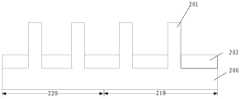
图1至图4是一种半导体器件的形成过程的剖面结构示意图。FIG. 1 to FIG. 4 are schematic cross-sectional structural diagrams of a process of forming a semiconductor device.
请参考图1,提供衬底100,所述衬底100包括外围区110和核心区120,所述外围区110和核心区120的衬底100表面分别具有鳍部101;在所述衬底100表面形成隔离层102;在所述隔离层102和鳍部101上形成介质层103,所述外围区110的介质层内具有第一开口111,所述核心区120的介质层内具有第二开口121,所述第一开口111和第二开口121底部的衬底上分别具有伪栅介质层104。Referring to FIG. 1 , a substrate 100 is provided, the substrate 100 includes a
请参考图2,在所述外围区110和所述核心区120的介质层103上、第一开口111的侧壁和底部、以及第二开口121的侧壁和底部形成第二保护层106;在所述第二保护层106上形成第一图形化层131,所述第一图形化层131暴露出所述第二开口121内的第二保护层106。Referring to FIG. 2 , a second
请参考图3,以第一图形化层131为掩膜,去除核心区120的介质层103上和所述第二开口121内的第二保护层106、以及第二开口121底部的伪栅介质层104。Referring to FIG. 3 , using the first patterned
请参考图4,在去除核心区120的介质层103上和所述第二开口121内的第二保护层106、以及第二开口121底部的伪栅介质层104之后,去除所述第一图形化层131(如图3所示);在去除图形化层131之后,去除所述外围区110的介质层103上和所述第一开口111内第二保护层106(如图3所示)。Referring to FIG. 4 , after removing the second
所述第一开口111和第二开口121在去除伪栅介质层上的伪栅层之后形成,由于所述伪栅介质层104在去除伪栅层的工艺中受到损伤,因此,所述核心区的伪栅介质层104并不适用于用作核心区器件的栅极氧化层,而外围区对于栅氧层的密度以及内部缺陷数量要求较低,因此能够保留外围区的所述伪栅介质层104。The
为了去除核心区120的伪栅介质层,保留外围区的伪栅介质层,需要在外围区形成第一图形化层131作为掩膜。而在形成第一图形化层131之前,所形成的第二保护层106能阻止所述核心区120和所述外围区110的伪栅介质层104发生反应,避免出现光刻胶残留以及膜层结构损伤。然而,由于在去除所述第一开口111内第二保护层106之前,已经暴露出核心区120鳍部101的部分侧壁和顶部表面,因此在刻蚀第二保护层106的过程中,对核心区120的鳍部101造成损伤。所述受损的鳍部101不仅容易引起经时击穿(Time DependentDielectric Breakdown,简称TDDB),导致短沟道效应,减少驱动电流,提高功耗,还容易引起偏压温度不稳定效应(Bias Temperature Instability,简称BTI),所形成的半导体结构性能变差。In order to remove the dummy gate dielectric layer in the
为了解决上述技术问题,本发明提供了一种半导体器件的形成方法,通过将核心区的第一保护层和第二保护层去除之后,然后在去除外围区的第二保护层的同时,将所述核心区的第一栅氧层去除,能够防止刻蚀工艺对于核心区的损伤,从而提高半导体器件的沟道区质量,减少漏电流,提高半导体器件的性能和可靠性。In order to solve the above-mentioned technical problems, the present invention provides a method for forming a semiconductor device. The removal of the first gate oxide layer in the core region can prevent damage to the core region caused by the etching process, thereby improving the quality of the channel region of the semiconductor device, reducing leakage current, and improving the performance and reliability of the semiconductor device.
为使本发明的上述目的、特征和优点能够更为明显易懂,下面结合附图对本发明的具体实施例做详细的说明。In order to make the above objects, features and advantages of the present invention more clearly understood, the specific embodiments of the present invention will be described in detail below with reference to the accompanying drawings.
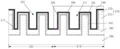
图5至图17是本发明实施例的半导体器件的形成过程的剖面结构示意图。5 to 17 are schematic cross-sectional structural diagrams of a process of forming a semiconductor device according to an embodiment of the present invention.
提供衬底,所述衬底包括核心区和外围区,所述衬底上具有介质结构,所述介质结构内具有第一开口和第二开口,所述第一开口位于外围区,所述第二开口位于核心区,所述第一开口和第二开口底部的衬底上分别具有第一栅氧层,所述第一栅氧层表面具有第一保护层。以下结合图5至图10对介质结构、第一开口、第二开口、第一栅氧层和第一保护层的形成过程进行说明。A substrate is provided, the substrate includes a core region and a peripheral region, the substrate has a dielectric structure, the dielectric structure has a first opening and a second opening, the first opening is located in the peripheral region, and the first opening is located in the peripheral region. Two openings are located in the core region, a first gate oxide layer is respectively formed on the substrate at the bottom of the first opening and the second opening, and a first protective layer is formed on the surface of the first gate oxide layer. The formation process of the dielectric structure, the first opening, the second opening, the first gate oxide layer and the first protective layer will be described below with reference to FIGS. 5 to 10 .
请参考图5,提供衬底,所述衬底包括核心区220和外围区210。Referring to FIG. 5 , a substrate is provided, and the substrate includes a
在本实施例中,所述衬底包括:基底200以及位于基底上的隔离层202。所述基底上具有鳍部201;所述隔离层覆盖所述鳍部的部分侧壁,且所述隔离层的顶部低于所述鳍部的顶部。In this embodiment, the substrate includes: a
在其它实施例中,所述衬底为平面基底。In other embodiments, the substrate is a planar substrate.
所述核心区220用于形成核心器件,所述外围区210用于形成外围器件。所述核心区220的核心器件密度大于外围区210的外围器件密度,且所述核心器件的特征尺寸(Critical Dimension,简称CD)小于所述外围区器件的特征尺寸。所述核心器件的工作电流或工作电压小于所述外围器件的工作电流或工作电压。The
在本实施例中,所述基底200和鳍部201的形成步骤包括:提供半导体基底;在所述半导体基底的部分表面形成初始图形化层,所述初始图形化层需要覆盖形成鳍部201的对应位置和形状;以所述初始图形化层为掩膜,刻蚀所述半导体基底,形成所述基底200和所述鳍部201。In this embodiment, the steps of forming the
所述半导体基底的材料可以是单晶硅、多晶硅或者非晶硅;半导体基底的材料也可以是硅、锗、锗化硅、砷化镓等半导体材料;所述半导体基底还可以是绝缘体上的硅、锗、锗化硅、砷化镓等半导体材料。在本实施例中,所述半导体基底为单晶硅衬底,即所述鳍部201和基底200的材料为单晶硅。The material of the semiconductor substrate can be single crystal silicon, polycrystalline silicon or amorphous silicon; the material of the semiconductor substrate can also be semiconductor materials such as silicon, germanium, silicon germanium, gallium arsenide, etc.; the semiconductor substrate can also be on an insulator Semiconductor materials such as silicon, germanium, silicon germanium, and gallium arsenide. In this embodiment, the semiconductor substrate is a single crystal silicon substrate, that is, the materials of the
在本实施例中,所述初始图形化层为光刻胶层,采用涂布工艺和光刻工艺形成。在另一实施例中,为了缩小所述鳍部201的特征尺寸,以及相邻鳍部201之间的距离,所述光刻胶层采用多重图形化掩膜工艺形成。In this embodiment, the initial patterning layer is a photoresist layer, which is formed by a coating process and a photolithography process. In another embodiment, in order to reduce the feature size of the
刻蚀所述半导体基底的工艺为各向异性的干法刻蚀工艺。所述鳍部201的侧壁相对于基底200的表面垂直或倾斜,且当所述鳍部201的侧壁相对于基底200表面倾斜时,所述鳍部201的底部尺寸大于顶部尺寸。在本实施例中,所述鳍部201的侧壁相对于基底200表面垂直。The process of etching the semiconductor substrate is an anisotropic dry etching process. The sidewalls of the
在另一实施例中,所述鳍部通过刻蚀形成于基底表面的半导体层上;所述半导体层采用选择性外延沉积工艺形成于所述基底表面。所述基底为硅、锗、锗化硅等基底,也可以为绝缘体上硅、锗、锗化硅等基底;所述基底还可以为玻璃基底或者III-V族化合物基底。所述半导体层的材料为硅、锗、碳化硅或硅锗。In another embodiment, the fins are formed on the semiconductor layer on the surface of the substrate by etching; the semiconductor layer is formed on the surface of the substrate by a selective epitaxial deposition process. The substrate may be a substrate such as silicon, germanium, silicon germanium, or the like, and may also be a substrate such as silicon-on-insulator, germanium, or silicon germanium; the substrate may also be a glass substrate or a III-V group compound substrate. The material of the semiconductor layer is silicon, germanium, silicon carbide or silicon germanium.
所述隔离层202的形成步骤包括:在所述基底200和鳍部201的表面形成隔离膜;平坦化所述隔离膜;在平坦或所述隔离膜之后,回刻蚀所述隔离膜直至暴露出部分鳍部201侧壁为止。The steps of forming the
在本实施例中,所述隔离层202的材料为氧化硅;所述隔离层202的厚度是所述鳍部201高度的1/4~1/2。所述隔离膜的形成工艺为流体化学气相沉积工艺(FlowableChemical Vapor Deposition,简称FCVD)。In this embodiment, the material of the
在其他实施例中,所述隔离膜还能够采用其他化学气相沉积工艺或物理气相沉积工艺形成;所述其他化学气相沉积工艺包括等离子体增强化学气相沉积工艺(PECVD)或者高深宽比化学气相沉积工艺(HARP)。In other embodiments, the isolation film can also be formed by other chemical vapor deposition processes or physical vapor deposition processes; the other chemical vapor deposition processes include plasma enhanced chemical vapor deposition (PECVD) or high aspect ratio chemical vapor deposition Process (HARP).
所述平坦化工艺为化学机械抛光工艺(CMP)。在本实施例中,所述化学机械抛光工艺以直至暴露出所述鳍部201的顶部表面为止。回刻蚀所述隔离膜的工艺为湿法刻蚀工艺或干法刻蚀工艺中的一种或两种组合。The planarization process is a chemical mechanical polishing process (CMP). In this embodiment, the chemical mechanical polishing process is performed until the top surface of the
请参考图6,在所述衬底的表面形成初始第一栅氧层213。Referring to FIG. 6, an initial first
所述初始第一栅氧层213作为伪栅介质层,用于在后续去除伪栅层时保护所述衬底的表面。The initial first
在本实施例中,所述初始第一栅氧层213用于形成后续外围区210的第一栅氧层,用于增强外围区210的鳍部201与后续形成的第一栅介质层之间的结合强度。In this embodiment, the initial first
在本实施例中,所述初始第一栅氧层213形成于所述基底200和所述鳍部201之上,并覆盖所述鳍部201的侧壁和顶部表面。In this embodiment, the initial first
在本实施例中,所述初始第一栅氧化层213的材料为氧化硅,所述第一栅氧化层213的形成工艺为原位蒸汽生成工艺(In-Situ Steam Generation,简称ISSG);所述初始第一栅氧层213的厚度为20埃~60埃。所述原位蒸汽生成工艺的参数包括:温度为700℃~1200℃,气体包括氢气和氧气,氧气流量为1slm~50slm,氢气流量为1slm~10slm,时间为10秒~5分钟。所述原位蒸汽生成工艺形成的初始第一栅氧层具有良好的阶梯覆盖能力,能够使所形成的初始第一栅氧层紧密地覆盖于所述鳍部201的侧壁表面,且所形成的所述初始第一栅氧层的厚度均匀。In this embodiment, the material of the initial first
在另一实施例中,所述初始第一栅氧层213的形成工艺为化学氧化工艺;所述化学氧化工艺的步骤包括:采用通入臭氧的水溶液对所述鳍部201暴露出的侧壁和顶部表面进行氧化,在所述鳍部201的侧壁和表面形成第一氧化层。其中,在所述通入臭氧的水溶液中,臭氧在水中的浓度为1%~15%。In another embodiment, the formation process of the initial first
请参考图7,对所述初始第一栅氧层213(如图6所示)进行表面处理,形成第一栅氧层203以及位于第一栅氧层203表面的第一保护层204。Referring to FIG. 7 , the initial first gate oxide layer 213 (as shown in FIG. 6 ) is subjected to surface treatment to form a first
所述表面处理的步骤包括:采用解耦等离子体氮化工艺对初始第一栅氧层表面进行处理,在所述第一栅氧层203表面形成初始保护层;对所述初始保护层进行退火工艺,形成第一保护层204。从所述第一保护层204的膜层外表面至所述第一保护层内表面的方向,氮的含量呈现逐步递减的趋势。The surface treatment step includes: using a decoupling plasma nitridation process to treat the surface of the initial first gate oxide layer, forming an initial protective layer on the surface of the first
所述第一栅氧层203并不适用于用作所述核心区220的器件的栅极氧化层,而所述外围区210对于栅氧层的密度以及内部缺陷数量要求较低,因此,能够保留所述外围区210的所述第一栅氧层203。The first
所述第一保护层204则能够在后续去除伪栅层的刻蚀工艺中,减少所述第一栅氧层203受到损伤。当后续去除伪栅层的刻蚀工艺包括等离子体干法刻蚀工艺时,所述等离子体刻蚀工艺容易对鳍部201的内部造成损伤,而所述第一保护层204的密度和硬度较高,从而能够用于阻挡等离子,避免鳍部201受到损伤,由此能够减少外围区210形成的半导体器件的漏电流,改善电学性能。The first
在本实施例中,所述第一栅氧层203的材料为氧化硅,所述第一保护层204的材料为氮氧化硅。In this embodiment, the material of the first
在本实施例中,所述第一保护层204覆盖暴露于所述隔离层202之上的所述鳍部201的侧壁和顶部表面。在后续去除伪栅层时,所述第一保护层204的密度和硬度有利于保护所述第一栅氧层203和鳍部201;而且,由于所述第一保护层204的介电系数较高,有利于抑制鳍部201与后续形成的第一栅介质层之间的载流子隧穿现象,减少漏电流。In this embodiment, the first
所述第一栅氧层203的厚度为10埃~50埃,所述第一保护层204的厚度为10埃~25埃。出于后续同时去除所述第一栅氧层和后续形成的第二保护层的目的,所述第一栅氧层203的厚度与后续第二保护层的厚度呈现对应关系。The thickness of the first
后续形成介质结构、第一开口和第二开口。以下结合图8至图10对所述介质结构、以及介质结构内的第一开口和第二开口的形成步骤进行说明。The dielectric structure, the first opening and the second opening are subsequently formed. The following describes the dielectric structure and the steps of forming the first opening and the second opening in the dielectric structure with reference to FIGS. 8 to 10 .
请参考图8,分别在所述核心区220和外围区210的衬底上形成伪栅极结构,所述伪栅极结构包括伪栅层205,所述伪栅层205位于第一保护层204之上。Referring to FIG. 8 , a dummy gate structure is formed on the substrates of the
所述伪栅层205的材料为多晶硅。所述伪栅层205的形成步骤包括:在所述第一保护层表面形成伪栅极膜;对所述伪栅极膜进行平坦化;在所述平坦化工艺之后,在所述伪栅极膜表面形成第二图形化层,所述第二图形化层覆盖需要形成伪栅层205的位置和形状;以所述第二图形化层为掩膜,刻蚀所述伪栅极膜,直至暴露出所述衬底的表面为止,形成伪栅层。The material of the
在本实施例中,还包括:在所述伪栅层205的侧壁表面形成侧墙215;在所述伪栅层205和侧墙两侧的鳍部201内形成源区和漏区。In this embodiment, the method further includes: forming
所述侧墙215的材料包括氧化硅、氮化硅和氮氧化硅中的一种或多种组合。所述侧墙215的形成步骤包括:采用沉积工艺在所述伪栅层205表面形成侧墙膜;回刻蚀所述侧墙膜直至暴露出所述伪栅层205的顶部表面,形成侧墙215。The material of the
所述源区和漏区的形成工艺为离子注入工艺和原位掺杂工艺中的一种或两种组合。在一实施例中,所述源区和漏区以离子注入工艺形成。在另一实施例中,所述源区和漏区的形成步骤还包括:在所述伪栅层205和侧墙215两侧的鳍部201内形成凹槽;采用选择性外延沉积工艺在所述凹槽内形成应力层;在所述应力层内掺杂离子,形成源区和漏区。当所形成的半导体器件为PMOS晶体管时,所述应力层的材料为硅锗,所述应力层内掺杂的离子为P型离子,且所述应力层为∑型应力层。当所形成的半导体器件为NMOS晶体管时,所述应力层的材料为碳化硅,所述应力层内掺杂的离子为N型离子。The formation process of the source region and the drain region is one or a combination of an ion implantation process and an in-situ doping process. In one embodiment, the source and drain regions are formed by an ion implantation process. In another embodiment, the forming step of the source region and the drain region further includes: forming grooves in the
请参考图9,在所述衬底上形成介质结构230,所述介质结构230覆盖所述伪栅极结构的侧壁,且所述介质结构230暴露出所述伪栅层205的顶部。Referring to FIG. 9 , a
所述介质结构230包括第一介质层231以及位于第一介质层231上的第二介质层232,且所述第二介质层232的硬度高于所述第一介质层231的硬度。所述第二介质层232由于硬度较高,用于在后续在进行研磨时作为第一介质层的保护层。其中所述第一介质层231的厚度为250埃~500埃,所述第二介质层232的厚度为300埃~1000埃。The
所述介质结构230的形成步骤包括:在所述隔离层202和所述伪栅层205的表面形成第一介质膜和第二介质膜;平坦化所述第一介质膜和第二介质膜直至暴露出所述伪栅层205的顶部表面为止,形成所述介质结构230。The steps of forming the
所述第一介质膜和所述第二介质膜的形成工艺为化学气相沉积工艺、物理气相沉积工艺和原子层沉积工艺的一种或多种组合。所述介质结构230的材料为氧化硅、氮化硅、氧氮化硅、低k介质材料(介电系数为大于或等于2.5,小于3.9,例如多孔氧化硅、或多孔氮化硅)或超低k介质材料(介电系数小于2.5,例如多孔SiCOH)中的一种或多种组合。The formation process of the first dielectric film and the second dielectric film is one or more combinations of chemical vapor deposition, physical vapor deposition and atomic layer deposition. The material of the
在本实施例中,所述第一介质层231和第二介质层232的材料为氧化硅。In this embodiment, the materials of the
请参考图10,去除所述伪栅层205(如图9所示)并暴露出所述第一保护层204,在所述外围区210的介质结构230内形成第一开口211,在所述核心区220的介质结构230内形成第二开口221。Referring to FIG. 10 , the dummy gate layer 205 (as shown in FIG. 9 ) is removed to expose the first
去除所述伪栅层205的工艺为干法刻蚀工艺、湿法刻蚀工艺中的一种或两种组合;其中,所述干法刻蚀工艺为各向异性的干法刻蚀工艺。The process of removing the
在本实施例中,所述伪栅层205的材料为多晶硅,去除所述伪栅层205的工艺为等离子干法刻蚀工艺。所述等离子体干法刻蚀工艺的参数包括:气体包括碳氟气体、HBr和Cl2中的一种或两种、以及载气,所述碳氟气体包括CF4、CHF3、CH2F2、CH3F;所述载气为惰性气体,例如He的气体流量为50sccm~400sccm,压强为3mtorr~8mtorr。In this embodiment, the material of the
在所述等离子体干法刻蚀工艺中,具有能量的等离子体容易对所述鳍部201内部造成损伤,而所述第一保护层204的密度和硬度较高,从而能够在扩散所述伪栅层205的过程中,阻挡所述等离子体的轰击,从而避免鳍部201内受到等离子体损伤。In the plasma dry etching process, the plasma with energy is likely to cause damage to the interior of the
在另一实施例中,去除所述伪栅极层205的工艺为湿法刻蚀工艺,所述湿法刻蚀工艺的刻蚀液为氢氟酸溶液。In another embodiment, the process of removing the
请参考图11,在所述核心区220和所述外围区210的介质结构230上、第一开口211的侧壁和底部、以及第二开口221的侧壁和底部形成第二保护层206。Referring to FIG. 11 , a second
在所述核心区220和所述外围区210表面形成所述第二保护层206,所述第二保护层206完全覆盖所述核心区220和所述外围区210的表面;当后续去除第一图形化层时,所述第二保护层206能阻止材质为氮氧化硅的所述第一保护层204发生反应,避免出现光刻胶残留以及膜层结构损伤。The second
所述第二保护层206的形成工艺为化学气相沉积工艺、物理气相沉积工艺和原子层沉积工艺中的一种或多种组合。所述第二保护层206在光刻工艺中能避免与光阻以及显影和剥离药液发生反应,因此,所述第二保护层206的材料为氧化硅或与之类似的具有相同特性的材料。The formation process of the second
在本实施例中,所述第二保护层206的材质为氧化硅,厚度为10埃~60埃。在后续工艺中,同时去除所述核心区220的所述第一栅氧层203和所述外围区210的所述的第二保护层206,所述第一栅氧层203的厚度与所述第二保护层206的厚度呈现对应关系。In this embodiment, the material of the second
请参考图12,在所述第二保护层206上形成第一图形化层240,所述第一图形化层240暴露出所述第二开口221内的第二保护层206。Referring to FIG. 12 , a first
所述第一图形化层240为图形化的光刻胶层,所述第一图形化层240填充满所述第一开口211。在本实施例中,所述第一图形化层240还覆盖于介质结构230的表面。The first
所述第一图形化层240的形成步骤包括:在所述第二保护层206上形成光刻胶层,所述光刻胶层填充满所述第一开口211和所述第二开口221;采用掩膜光刻工艺对光刻胶层形成初始图形化层;在形成初始图形化层之后,对光刻胶进行图形化,形成第一图形化层240。The step of forming the first patterned
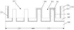
请参考图13,以第一图形化层240为掩膜,去除所述第二开口221内的第二保护层206(如图12所示)和第一保护层204(如图12所示),暴露出所述第二开口221底部的第一栅氧层203。Referring to FIG. 13 , using the first patterned
去除所述第二开口221内的第二保护层206和第一保护层204的步骤包括:以第一图形化层240为掩膜,去除所述第二开口221内的第二保护层206;以第一图形化层240为掩膜,去除所述第二开口221内的第一保护层204,暴露出所述第二开口221底部的第一栅氧层203。The step of removing the second
所述外围区210对于栅氧层的密度以及内部缺陷数量要求较低,因此,能够保留所述外围区210的所述第一栅氧层203。The
去除所述第二开口221内的第二保护层206和第一保护层204的工艺为湿法刻蚀工艺和干法刻蚀工艺中的一种或两种组合。The process of removing the second
在本实施例中,所述第二保护层206的材料为氧化硅,去除所述第二保护层206的工艺为湿法刻蚀工艺;所述第一保护层204的材料为氧化硅,去除所述第一保护层204的工艺为干法刻蚀工艺,所述干法刻蚀工艺为各向异性的干法刻蚀工艺。In this embodiment, the material of the second
去除所述第二保护层206的工艺为湿法刻蚀工艺。所述湿法刻蚀工艺的参数包括:氢氟酸与水的质量百分比为1:500~1:2000,刻蚀时间5秒~1000秒,过刻量50%~300%。The process of removing the second
所述湿法刻蚀工艺采用氢氟酸去除氧化硅,由于氢氟酸的刻蚀选择性,不会对位于所述第二保护层206下方的材料为氮氧化硅的所述第一保护层204产生刻蚀。由于氢原子与氟原子间结合的能力相对较强,使得氢氟酸在水中不能完全被电离,理论上低浓度的所述氢氟酸是一种弱酸。但当浓度较低时,所述湿法刻蚀速率过慢,不利用高效生产;而当浓度过高时,氢氟酸在与所述材料为氧化硅的第二保护层206反应时,生成物可以继续和过量的氢氟酸反应,生成强酸性的氟硅酸而导致产生副反应,因此,所述湿法刻蚀工艺中对于氢氟酸与水的质量百分比需进行控制。The wet etching process uses hydrofluoric acid to remove silicon oxide. Due to the etching selectivity of hydrofluoric acid, the first protective layer under the second
在本实施例中,去除所述第一保护层204的工艺为干法刻蚀工艺能够为干法刻蚀工艺,所述干法刻蚀工艺为各向同性的SICONI干法刻蚀工艺。所述SICONI干法刻蚀工艺在各个不同方向上的刻蚀速率均匀,能够均匀地去除位于鳍部201侧壁和顶部表面的第一保护层204。In this embodiment, the process for removing the first
所述SICONI干法刻蚀工艺的参数包括:He的气体流量为600sccm~2000sccm,NH3的气体流量为200sccm~500sccm,NF3的气体流量为20sccm~200sccm;压强为2torr~10torr,刻蚀时间5秒~100秒,过刻量50%~100%。The parameters of the SICONI dry etching process include: the gas flow rate of He is 600sccm-2000sccm, the gas flow rate of NH3 is 200sccm-500sccm, the gas flow rate of NF3 is 20sccm-200sccm; the pressure is 2torr-10torr, and the etching time is 5 seconds to 100 seconds, over-scale 50% to 100%.
请参考图14,在去除所述第二开口221内的第二保护层206(如图12所示)和第一保护层204(如图12所示)之后,去除所述第一图形化层240(如图13所示)。Referring to FIG. 14 , after removing the second protective layer 206 (shown in FIG. 12 ) and the first protective layer 204 (shown in FIG. 12 ) in the
在本实施例中,去除所述第一图形化层240的过程中,所述第二保护层206用于保护第一保护层204,避免材质为氮氧化硅的第一保护层204发生反应而出现损伤。去除所述第一图形化层240的工艺为灰化工艺和湿法工艺中的一种或两种组合。In this embodiment, during the process of removing the first patterned
在本实施列中,去除所述第一图形化层240的工艺为灰化工艺和湿法工艺的组合工艺。其中,所述灰化工艺的参数包括:压强为50mtorr~900mtorr,功率1000w~2700w,N2的气体流量为500sccm~4000sccm,H2的气体流量为50sccm~1000sccm,温度为80℃~250℃。其中,所述湿法工艺的参数包括:H2SO4和水的体积百分比为3:1~6:1,温度100℃~130℃。In this embodiment, the process of removing the first patterned
所述灰化工艺为等离子体灰化工艺,在灰化去除材料为光刻胶的所述第一图形化层240之后,等离子体处理会在衬底的表面残留大量有机物,这要求必须通过强的氧化溶剂进行清除。所述湿法工艺中通过含有H2SO4的水溶液来清除等离子导致的有机物或聚合物残留,确保衬底表面的洁净度,避免产生工艺缺陷。The ashing process is a plasma ashing process. After the first patterned
请参考图15,在去除所述第一图形化层240(如图13所示)之后,去除所述第二开口221底部的第一栅氧层203(如图14所示)和所述第一开口211内的第二保护层206(如图14所示),暴露出所述第一开口211底部的第一保护层204。Referring to FIG. 15 , after removing the first patterned layer 240 (as shown in FIG. 13 ), remove the first gate oxide layer 203 (as shown in FIG. 14 ) and the first gate oxide layer 203 (as shown in FIG. 14 ) at the bottom of the
去除所述第二开口221底部的第一栅氧层203和所述第一开口211内的第二保护层206的工艺为湿法刻蚀工艺或各向同性的干法刻工艺中的一种或两种组合。The process of removing the first
所述第一栅氧层203和所述第二保护层206的材料均为氧化硅,且位于所述第一栅氧层203之下为核心区220鳍部201,位于所述第二保护层206之下为外围区210的所述第一保护层204。干法刻蚀工艺中的等离子体的轰击,很容易对所述第一栅氧层203之下的核心区220鳍部201造成损伤,因此,优选用湿法刻蚀工艺用于去除第一栅氧层203和所述第二保护层206。The materials of the first
在本实施例中,去除第一栅氧层203和所述第二保护层206的工艺为湿法刻蚀工艺,参数包括:氢氟酸与水的质量百分比为1:500~1:2000,刻蚀时间5秒~1000秒,过刻量50%~300%。In this embodiment, the process of removing the first
请参考图16,在去除所述第二开口221底部的第一栅氧层203(如图14所示)和所述第一开口211内的第二保护层206(如图14所示)之后,在所述第二开口221底部形成第二栅氧层207。Referring to FIG. 16 , after removing the first
所述第二栅氧层207用作核心区220形成的半导体器件的栅氧层。所述第二栅氧层207的材料为氧化硅;所述第二栅氧层207的形成工艺为热氧化工艺或湿法氧化工艺。The second
所述第二栅氧层207的厚度为8埃~15埃。在本实施例中,所述第二栅氧层207的形成工艺为热氧化工艺。所述热氧化工艺的参数包括:时间100秒~1000秒,压强为50mtorr~~300torr,氧气与氮气的气体流量比为1/20~1/5。The thickness of the second
请参考图17,在所述外围区210的第一保护层204表面形成填充所述第一开口211的第一栅极结构;在所述核心区220的第二栅氧层207表面形成填充所述第二开口221的第二栅极结构。Referring to FIG. 17 , a first gate structure filling the
所述第一栅极结构包括位于所述第一保护层204上的第一栅介质层212,所述第一栅介质层212覆盖所述外围区210的介质结构230的顶部表面和所述第一开口211的侧壁和底部表面;所述第二栅极结构包括位于所述第二栅氧层207上的第二栅介质层222,所述第二栅介质层222覆盖所述核心区220的介质结构230的顶部表面和所述第二开口221的侧壁和底部表面。The first gate structure includes a first gate dielectric layer 212 on the first
所述第一栅介质层212和所述第二栅介质层222的材料为高k介质材料(介电系数大于3.9);所述高k介质材料包括氧化铪、氧化锆、氧化铪硅、氧化镧、氧化锆硅、氧化钛、氧化钽、氧化钡锶钛、氧化钡钛、氧化锶钛或氧化铝。The materials of the first gate dielectric layer 212 and the second
所述第一栅介质层212和所述第二栅介质层222的形成步骤为化学气相沉积工艺、物理气相沉积工艺或原子层沉积工艺的一种或多种组合。The first gate dielectric layer 212 and the second
在一实施例中,第一栅极结构还包括位于第一栅介质层212表面的第一功函数层,第二栅极结构还包括位于第二栅介质层222表面的第二功函数层。具体的,在形成所述第一栅介质层212和所述第二栅介质层222之后,在所述第一栅介质层212表面形成第一功函数层,在所述第二栅介质层222表面形成第二功函数层。形成所述第一功函数层和第二功函数层的工艺步骤包括:在所述第一栅介质层212和所述第二栅介质层222的表面形成功函数膜,且所述功函数膜覆盖所述介质结构230的顶部表面;平坦化所述功函数膜,直至暴露出所述介质结构230的表面为止,形成第一功函数层和第二功函数层。在第一功函数层的材料和第二功函数层的材料能够相同或不同。In one embodiment, the first gate structure further includes a first work function layer on the surface of the first gate dielectric layer 212 , and the second gate structure further includes a second work function layer on the surface of the second
综上,本实施例中,在去除所述核心区的第二保护层和第一保护层之后,此时衬底表面暴露出核心区的第一栅氧层和所述外围区的第二保护层,由于所述第一栅氧层和第二保护层的材料均为氧化硅,因此在去除外围区的第二保护层的同时,可将所述核心区的第一栅氧层去除,降低了核心区鳍部暴露在刻蚀环境中的风险,从而高半导体器件的沟道区质量,减少漏电流,提高半导体器件的性能和可靠性。To sum up, in this embodiment, after the second protective layer and the first protective layer in the core region are removed, the surface of the substrate exposes the first gate oxide layer in the core region and the second protective layer in the peripheral region. Since the materials of the first gate oxide layer and the second protective layer are both silicon oxide, while removing the second protective layer in the peripheral region, the first gate oxide layer in the core region can be removed, reducing the The risk of exposure of the fins in the core region to the etching environment is avoided, so that the quality of the channel region of the semiconductor device is improved, the leakage current is reduced, and the performance and reliability of the semiconductor device are improved.
虽然本发明披露如上,但本发明并非限定于此。任何本领域技术人员,在不脱离本发明的精神和范围内,均可作各种更动与修改,因此本发明的保护范围应当以权利要求所限定的范围为准。Although the present invention is disclosed above, the present invention is not limited thereto. Any person skilled in the art can make various changes and modifications without departing from the spirit and scope of the present invention. Therefore, the protection scope of the present invention should be based on the scope defined by the claims.
Claims (20)
Priority Applications (1)
| Application Number | Priority Date | Filing Date | Title |
|---|---|---|---|
| CN201710304556.3ACN108807377B (en) | 2017-05-03 | 2017-05-03 | Semiconductor device and method of forming the same |
Applications Claiming Priority (1)
| Application Number | Priority Date | Filing Date | Title |
|---|---|---|---|
| CN201710304556.3ACN108807377B (en) | 2017-05-03 | 2017-05-03 | Semiconductor device and method of forming the same |
Publications (2)
| Publication Number | Publication Date |
|---|---|
| CN108807377A CN108807377A (en) | 2018-11-13 |
| CN108807377Btrue CN108807377B (en) | 2020-07-10 |
Family
ID=64053589
Family Applications (1)
| Application Number | Title | Priority Date | Filing Date |
|---|---|---|---|
| CN201710304556.3AActiveCN108807377B (en) | 2017-05-03 | 2017-05-03 | Semiconductor device and method of forming the same |
Country Status (1)
| Country | Link |
|---|---|
| CN (1) | CN108807377B (en) |
Families Citing this family (5)
| Publication number | Priority date | Publication date | Assignee | Title |
|---|---|---|---|---|
| CN111863609B (en)* | 2019-04-30 | 2023-03-10 | 中芯国际集成电路制造(上海)有限公司 | Semiconductor structure and forming method thereof |
| CN111696860B (en)* | 2020-07-23 | 2022-11-04 | 上海华力微电子有限公司 | Semiconductor structure and manufacturing method thereof |
| CN115223872A (en)* | 2021-04-21 | 2022-10-21 | 中芯国际集成电路制造(上海)有限公司 | Semiconductor structure and method of forming the same |
| CN115881540A (en)* | 2021-09-27 | 2023-03-31 | 中芯国际集成电路制造(上海)有限公司 | Formation method of semiconductor structure |
| CN117790318B (en)* | 2024-02-27 | 2024-05-24 | 合肥晶合集成电路股份有限公司 | Semiconductor device and preparation method thereof |
Family Cites Families (3)
| Publication number | Priority date | Publication date | Assignee | Title |
|---|---|---|---|---|
| US7855105B1 (en)* | 2009-06-18 | 2010-12-21 | International Business Machines Corporation | Planar and non-planar CMOS devices with multiple tuned threshold voltages |
| CN104752221B (en)* | 2013-12-31 | 2017-11-03 | 中芯国际集成电路制造(上海)有限公司 | The forming method of fin formula field effect transistor |
| CN104979198B (en)* | 2014-04-02 | 2018-03-30 | 中芯国际集成电路制造(上海)有限公司 | The forming method of fin formula field effect transistor |
- 2017
- 2017-05-03CNCN201710304556.3Apatent/CN108807377B/enactiveActive
Also Published As
| Publication number | Publication date |
|---|---|
| CN108807377A (en) | 2018-11-13 |
Similar Documents
| Publication | Publication Date | Title |
|---|---|---|
| CN104008994B (en) | Manufacturing method of semiconductor device | |
| CN107039272B (en) | Method for forming fin type transistor | |
| CN108807377B (en) | Semiconductor device and method of forming the same | |
| CN107591362B (en) | Semiconductor structure and forming method thereof | |
| CN109390235B (en) | Semiconductor structure and forming method thereof | |
| CN108321090B (en) | Semiconductor device and method of forming the same | |
| CN106952816B (en) | Method of forming a fin transistor | |
| CN106876274A (en) | The forming method of transistor | |
| CN109148296B (en) | Semiconductor structure and method of forming the same | |
| CN107978514B (en) | Transistor and method of forming the same | |
| CN110890279A (en) | Semiconductor structure and method of forming the same | |
| CN109980003A (en) | Semiconductor devices and forming method thereof | |
| CN107045981B (en) | Formation method of semiconductor structure | |
| CN104103589B (en) | A kind of transistor fabrication process | |
| CN105826364A (en) | Transistor and formation method thereof | |
| CN106653693B (en) | Methods for improving the performance of core devices and I/O devices | |
| CN109300844B (en) | Fin type transistor and forming method thereof | |
| CN112151382A (en) | Semiconductor structure and forming method thereof | |
| CN107170685B (en) | Method for forming fin type transistor | |
| CN108206159B (en) | Semiconductor structure and method of forming the same | |
| CN113130312B (en) | Method for forming semiconductor structure | |
| CN112117192B (en) | Method for forming semiconductor structure | |
| JP4082280B2 (en) | Semiconductor device and manufacturing method thereof | |
| CN104347377B (en) | The forming method of NMOS metal gate transistors | |
| KR102610396B1 (en) | Method for providing a low-k spacer |
Legal Events
| Date | Code | Title | Description |
|---|---|---|---|
| PB01 | Publication | ||
| PB01 | Publication | ||
| SE01 | Entry into force of request for substantive examination | ||
| SE01 | Entry into force of request for substantive examination | ||
| GR01 | Patent grant | ||
| GR01 | Patent grant |