CN108780735B - Selective Deposition of Silicon Nitride Films for Spacer Applications - Google Patents
Selective Deposition of Silicon Nitride Films for Spacer ApplicationsDownload PDFInfo
- Publication number
- CN108780735B CN108780735BCN201780015644.XACN201780015644ACN108780735BCN 108780735 BCN108780735 BCN 108780735BCN 201780015644 ACN201780015644 ACN 201780015644ACN 108780735 BCN108780735 BCN 108780735B
- Authority
- CN
- China
- Prior art keywords
- processing
- film
- plasma
- substrate surface
- feature
- Prior art date
- Legal status (The legal status is an assumption and is not a legal conclusion. Google has not performed a legal analysis and makes no representation as to the accuracy of the status listed.)
- Active
Links
- 230000008021depositionEffects0.000titleclaimsabstractdescription33
- 229910052581Si3N4Inorganic materials0.000titleclaimsdescription24
- HQVNEWCFYHHQES-UHFFFAOYSA-Nsilicon nitrideChemical groupN12[Si]34N5[Si]62N3[Si]51N64HQVNEWCFYHHQES-UHFFFAOYSA-N0.000titleclaimsdescription23
- 125000006850spacer groupChemical group0.000titleabstractdescription10
- 238000012545processingMethods0.000claimsabstractdescription174
- 238000000034methodMethods0.000claimsabstractdescription77
- 239000000758substrateSubstances0.000claimsdescription138
- 239000007789gasSubstances0.000claimsdescription132
- IJGRMHOSHXDMSA-UHFFFAOYSA-NAtomic nitrogenChemical compoundN#NIJGRMHOSHXDMSA-UHFFFAOYSA-N0.000claimsdescription93
- 229910052757nitrogenInorganic materials0.000claimsdescription47
- 230000008569processEffects0.000claimsdescription45
- QGZKDVFQNNGYKY-UHFFFAOYSA-NAmmoniaChemical compoundNQGZKDVFQNNGYKY-UHFFFAOYSA-N0.000claimsdescription36
- 239000002243precursorSubstances0.000claimsdescription26
- 239000012686silicon precursorSubstances0.000claimsdescription25
- 239000000376reactantSubstances0.000claimsdescription24
- XKRFYHLGVUSROY-UHFFFAOYSA-NArgonChemical compound[Ar]XKRFYHLGVUSROY-UHFFFAOYSA-N0.000claimsdescription14
- 150000002500ionsChemical class0.000claimsdescription14
- 229910021529ammoniaInorganic materials0.000claimsdescription13
- 229910052786argonInorganic materials0.000claimsdescription8
- MROCJMGDEKINLD-UHFFFAOYSA-NdichlorosilaneChemical compoundCl[SiH2]ClMROCJMGDEKINLD-UHFFFAOYSA-N0.000claimsdescription8
- 229910052734heliumInorganic materials0.000claimsdescription8
- 239000001257hydrogenSubstances0.000claimsdescription8
- 229910052739hydrogenInorganic materials0.000claimsdescription8
- 239000001307heliumSubstances0.000claimsdescription7
- SWQJXJOGLNCZEY-UHFFFAOYSA-Nhelium atomChemical compound[He]SWQJXJOGLNCZEY-UHFFFAOYSA-N0.000claimsdescription7
- QVGXLLKOCUKJST-UHFFFAOYSA-Natomic oxygenChemical compound[O]QVGXLLKOCUKJST-UHFFFAOYSA-N0.000claimsdescription5
- 229910052760oxygenInorganic materials0.000claimsdescription5
- 239000001301oxygenSubstances0.000claimsdescription5
- 230000008859changeEffects0.000claimsdescription3
- QJGQUHMNIGDVPM-UHFFFAOYSA-Nnitrogen groupChemical group[N]QJGQUHMNIGDVPM-UHFFFAOYSA-N0.000claimsdescription3
- 239000000203mixtureSubstances0.000claimsdescription2
- 125000004435hydrogen atomChemical class[H]*0.000claims1
- 239000010408filmSubstances0.000description109
- 210000002381plasmaAnatomy0.000description64
- 238000009826distributionMethods0.000description41
- 238000000151depositionMethods0.000description34
- 235000012431wafersNutrition0.000description24
- 238000000231atomic layer depositionMethods0.000description18
- 238000010926purgeMethods0.000description15
- 238000000429assemblyMethods0.000description13
- 230000000712assemblyEffects0.000description13
- XUIMIQQOPSSXEZ-UHFFFAOYSA-NSiliconChemical compound[Si]XUIMIQQOPSSXEZ-UHFFFAOYSA-N0.000description12
- 229910052710siliconInorganic materials0.000description12
- 239000010703siliconSubstances0.000description12
- 239000000463materialSubstances0.000description9
- 230000002093peripheral effectEffects0.000description8
- 238000012546transferMethods0.000description8
- 238000005530etchingMethods0.000description6
- 238000003672processing methodMethods0.000description6
- 238000011282treatmentMethods0.000description6
- UFHFLCQGNIYNRP-UHFFFAOYSA-NHydrogenChemical compound[H][H]UFHFLCQGNIYNRP-UHFFFAOYSA-N0.000description5
- 239000003153chemical reaction reagentSubstances0.000description5
- 229910000069nitrogen hydrideInorganic materials0.000description5
- 239000000126substanceSubstances0.000description5
- 238000000137annealingMethods0.000description4
- 238000006243chemical reactionMethods0.000description4
- 238000005229chemical vapour depositionMethods0.000description4
- 238000010586diagramMethods0.000description4
- 239000011261inert gasSubstances0.000description4
- 230000015572biosynthetic processEffects0.000description3
- 238000001312dry etchingMethods0.000description3
- 238000004519manufacturing processMethods0.000description3
- 239000012528membraneSubstances0.000description3
- 238000002156mixingMethods0.000description3
- 150000004767nitridesChemical class0.000description3
- 238000000926separation methodMethods0.000description3
- 238000001039wet etchingMethods0.000description3
- VYPSYNLAJGMNEJ-UHFFFAOYSA-NSilicium dioxideChemical compoundO=[Si]=OVYPSYNLAJGMNEJ-UHFFFAOYSA-N0.000description2
- 230000000694effectsEffects0.000description2
- 238000010574gas phase reactionMethods0.000description2
- 150000002431hydrogenChemical class0.000description2
- 229910052751metalInorganic materials0.000description2
- 239000002184metalSubstances0.000description2
- 230000004048modificationEffects0.000description2
- 238000012986modificationMethods0.000description2
- VYIRVGYSUZPNLF-UHFFFAOYSA-Nn-(tert-butylamino)silyl-2-methylpropan-2-amineChemical compoundCC(C)(C)N[SiH2]NC(C)(C)CVYIRVGYSUZPNLF-UHFFFAOYSA-N0.000description2
- SSCVMVQLICADPI-UHFFFAOYSA-Nn-methyl-n-[tris(dimethylamino)silyl]methanamineChemical compoundCN(C)[Si](N(C)C)(N(C)C)N(C)CSSCVMVQLICADPI-UHFFFAOYSA-N0.000description2
- 238000005240physical vapour depositionMethods0.000description2
- 238000000623plasma-assisted chemical vapour depositionMethods0.000description2
- 238000012805post-processingMethods0.000description2
- 230000009257reactivityEffects0.000description2
- 239000004065semiconductorSubstances0.000description2
- 229910052814silicon oxideInorganic materials0.000description2
- 230000002123temporal effectEffects0.000description2
- 239000010409thin filmSubstances0.000description2
- JBRZTFJDHDCESZ-UHFFFAOYSA-NAsGaChemical compound[As]#[Ga]JBRZTFJDHDCESZ-UHFFFAOYSA-N0.000description1
- 229910018557Si OInorganic materials0.000description1
- BLRPTPMANUNPDV-UHFFFAOYSA-NSilaneChemical compound[SiH4]BLRPTPMANUNPDV-UHFFFAOYSA-N0.000description1
- 239000012080ambient airSubstances0.000description1
- 229910021417amorphous siliconInorganic materials0.000description1
- 125000004429atomChemical group0.000description1
- 238000004140cleaningMethods0.000description1
- 238000004891communicationMethods0.000description1
- 239000004020conductorSubstances0.000description1
- 238000010276constructionMethods0.000description1
- 238000011109contaminationMethods0.000description1
- 238000001816coolingMethods0.000description1
- 238000012864cross contaminationMethods0.000description1
- 125000004122cyclic groupChemical group0.000description1
- PZPGRFITIJYNEJ-UHFFFAOYSA-NdisilaneChemical compound[SiH3][SiH3]PZPGRFITIJYNEJ-UHFFFAOYSA-N0.000description1
- 238000001900extreme ultraviolet lithographyMethods0.000description1
- 229910052732germaniumInorganic materials0.000description1
- GNPVGFCGXDBREM-UHFFFAOYSA-Ngermanium atomChemical compound[Ge]GNPVGFCGXDBREM-UHFFFAOYSA-N0.000description1
- 239000011521glassSubstances0.000description1
- 238000010438heat treatmentMethods0.000description1
- 230000033444hydroxylationEffects0.000description1
- 238000005805hydroxylation reactionMethods0.000description1
- 239000012535impuritySubstances0.000description1
- 238000011065in-situ storageMethods0.000description1
- 239000012212insulatorSubstances0.000description1
- 238000011068loading methodMethods0.000description1
- 238000003754machiningMethods0.000description1
- 229910001092metal group alloyInorganic materials0.000description1
- 150000002739metalsChemical class0.000description1
- 230000005012migrationEffects0.000description1
- 238000013508migrationMethods0.000description1
- OWKFQWAGPHVFRF-UHFFFAOYSA-Nn-(diethylaminosilyl)-n-ethylethanamineChemical compoundCCN(CC)[SiH2]N(CC)CCOWKFQWAGPHVFRF-UHFFFAOYSA-N0.000description1
- 125000004433nitrogen atomChemical groupN*0.000description1
- 230000003647oxidationEffects0.000description1
- 238000007254oxidation reactionMethods0.000description1
- 238000000059patterningMethods0.000description1
- 238000007781pre-processingMethods0.000description1
- 230000001737promoting effectEffects0.000description1
- 238000005086pumpingMethods0.000description1
- 238000000746purificationMethods0.000description1
- 229910052594sapphireInorganic materials0.000description1
- 239000010980sapphireSubstances0.000description1
- LIVNPJMFVYWSIS-UHFFFAOYSA-Nsilicon monoxideInorganic materials[Si-]#[O+]LIVNPJMFVYWSIS-UHFFFAOYSA-N0.000description1
- 238000006557surface reactionMethods0.000description1
Images


Classifications
- H—ELECTRICITY
- H01—ELECTRIC ELEMENTS
- H01L—SEMICONDUCTOR DEVICES NOT COVERED BY CLASS H10
- H01L21/00—Processes or apparatus adapted for the manufacture or treatment of semiconductor or solid state devices or of parts thereof
- H01L21/02—Manufacture or treatment of semiconductor devices or of parts thereof
- H01L21/02104—Forming layers
- H01L21/02107—Forming insulating materials on a substrate
- H01L21/02109—Forming insulating materials on a substrate characterised by the type of layer, e.g. type of material, porous/non-porous, pre-cursors, mixtures or laminates
- H01L21/02112—Forming insulating materials on a substrate characterised by the type of layer, e.g. type of material, porous/non-porous, pre-cursors, mixtures or laminates characterised by the material of the layer
- H01L21/02123—Forming insulating materials on a substrate characterised by the type of layer, e.g. type of material, porous/non-porous, pre-cursors, mixtures or laminates characterised by the material of the layer the material containing silicon
- H01L21/0217—Forming insulating materials on a substrate characterised by the type of layer, e.g. type of material, porous/non-porous, pre-cursors, mixtures or laminates characterised by the material of the layer the material containing silicon the material being a silicon nitride not containing oxygen, e.g. SixNy or SixByNz
- C—CHEMISTRY; METALLURGY
- C23—COATING METALLIC MATERIAL; COATING MATERIAL WITH METALLIC MATERIAL; CHEMICAL SURFACE TREATMENT; DIFFUSION TREATMENT OF METALLIC MATERIAL; COATING BY VACUUM EVAPORATION, BY SPUTTERING, BY ION IMPLANTATION OR BY CHEMICAL VAPOUR DEPOSITION, IN GENERAL; INHIBITING CORROSION OF METALLIC MATERIAL OR INCRUSTATION IN GENERAL
- C23C—COATING METALLIC MATERIAL; COATING MATERIAL WITH METALLIC MATERIAL; SURFACE TREATMENT OF METALLIC MATERIAL BY DIFFUSION INTO THE SURFACE, BY CHEMICAL CONVERSION OR SUBSTITUTION; COATING BY VACUUM EVAPORATION, BY SPUTTERING, BY ION IMPLANTATION OR BY CHEMICAL VAPOUR DEPOSITION, IN GENERAL
- C23C16/00—Chemical coating by decomposition of gaseous compounds, without leaving reaction products of surface material in the coating, i.e. chemical vapour deposition [CVD] processes
- C23C16/04—Coating on selected surface areas, e.g. using masks
- C23C16/045—Coating cavities or hollow spaces, e.g. interior of tubes; Infiltration of porous substrates
- C—CHEMISTRY; METALLURGY
- C23—COATING METALLIC MATERIAL; COATING MATERIAL WITH METALLIC MATERIAL; CHEMICAL SURFACE TREATMENT; DIFFUSION TREATMENT OF METALLIC MATERIAL; COATING BY VACUUM EVAPORATION, BY SPUTTERING, BY ION IMPLANTATION OR BY CHEMICAL VAPOUR DEPOSITION, IN GENERAL; INHIBITING CORROSION OF METALLIC MATERIAL OR INCRUSTATION IN GENERAL
- C23C—COATING METALLIC MATERIAL; COATING MATERIAL WITH METALLIC MATERIAL; SURFACE TREATMENT OF METALLIC MATERIAL BY DIFFUSION INTO THE SURFACE, BY CHEMICAL CONVERSION OR SUBSTITUTION; COATING BY VACUUM EVAPORATION, BY SPUTTERING, BY ION IMPLANTATION OR BY CHEMICAL VAPOUR DEPOSITION, IN GENERAL
- C23C16/00—Chemical coating by decomposition of gaseous compounds, without leaving reaction products of surface material in the coating, i.e. chemical vapour deposition [CVD] processes
- C23C16/22—Chemical coating by decomposition of gaseous compounds, without leaving reaction products of surface material in the coating, i.e. chemical vapour deposition [CVD] processes characterised by the deposition of inorganic material, other than metallic material
- C23C16/30—Deposition of compounds, mixtures or solid solutions, e.g. borides, carbides, nitrides
- C23C16/34—Nitrides
- C23C16/345—Silicon nitride
- C—CHEMISTRY; METALLURGY
- C23—COATING METALLIC MATERIAL; COATING MATERIAL WITH METALLIC MATERIAL; CHEMICAL SURFACE TREATMENT; DIFFUSION TREATMENT OF METALLIC MATERIAL; COATING BY VACUUM EVAPORATION, BY SPUTTERING, BY ION IMPLANTATION OR BY CHEMICAL VAPOUR DEPOSITION, IN GENERAL; INHIBITING CORROSION OF METALLIC MATERIAL OR INCRUSTATION IN GENERAL
- C23C—COATING METALLIC MATERIAL; COATING MATERIAL WITH METALLIC MATERIAL; SURFACE TREATMENT OF METALLIC MATERIAL BY DIFFUSION INTO THE SURFACE, BY CHEMICAL CONVERSION OR SUBSTITUTION; COATING BY VACUUM EVAPORATION, BY SPUTTERING, BY ION IMPLANTATION OR BY CHEMICAL VAPOUR DEPOSITION, IN GENERAL
- C23C16/00—Chemical coating by decomposition of gaseous compounds, without leaving reaction products of surface material in the coating, i.e. chemical vapour deposition [CVD] processes
- C23C16/44—Chemical coating by decomposition of gaseous compounds, without leaving reaction products of surface material in the coating, i.e. chemical vapour deposition [CVD] processes characterised by the method of coating
- C23C16/455—Chemical coating by decomposition of gaseous compounds, without leaving reaction products of surface material in the coating, i.e. chemical vapour deposition [CVD] processes characterised by the method of coating characterised by the method used for introducing gases into reaction chamber or for modifying gas flows in reaction chamber
- C23C16/45519—Inert gas curtains
- C—CHEMISTRY; METALLURGY
- C23—COATING METALLIC MATERIAL; COATING MATERIAL WITH METALLIC MATERIAL; CHEMICAL SURFACE TREATMENT; DIFFUSION TREATMENT OF METALLIC MATERIAL; COATING BY VACUUM EVAPORATION, BY SPUTTERING, BY ION IMPLANTATION OR BY CHEMICAL VAPOUR DEPOSITION, IN GENERAL; INHIBITING CORROSION OF METALLIC MATERIAL OR INCRUSTATION IN GENERAL
- C23C—COATING METALLIC MATERIAL; COATING MATERIAL WITH METALLIC MATERIAL; SURFACE TREATMENT OF METALLIC MATERIAL BY DIFFUSION INTO THE SURFACE, BY CHEMICAL CONVERSION OR SUBSTITUTION; COATING BY VACUUM EVAPORATION, BY SPUTTERING, BY ION IMPLANTATION OR BY CHEMICAL VAPOUR DEPOSITION, IN GENERAL
- C23C16/00—Chemical coating by decomposition of gaseous compounds, without leaving reaction products of surface material in the coating, i.e. chemical vapour deposition [CVD] processes
- C23C16/44—Chemical coating by decomposition of gaseous compounds, without leaving reaction products of surface material in the coating, i.e. chemical vapour deposition [CVD] processes characterised by the method of coating
- C23C16/455—Chemical coating by decomposition of gaseous compounds, without leaving reaction products of surface material in the coating, i.e. chemical vapour deposition [CVD] processes characterised by the method of coating characterised by the method used for introducing gases into reaction chamber or for modifying gas flows in reaction chamber
- C23C16/45523—Pulsed gas flow or change of composition over time
- C23C16/45525—Atomic layer deposition [ALD]
- C23C16/45527—Atomic layer deposition [ALD] characterized by the ALD cycle, e.g. different flows or temperatures during half-reactions, unusual pulsing sequence, use of precursor mixtures or auxiliary reactants or activations
- C23C16/45536—Use of plasma, radiation or electromagnetic fields
- C—CHEMISTRY; METALLURGY
- C23—COATING METALLIC MATERIAL; COATING MATERIAL WITH METALLIC MATERIAL; CHEMICAL SURFACE TREATMENT; DIFFUSION TREATMENT OF METALLIC MATERIAL; COATING BY VACUUM EVAPORATION, BY SPUTTERING, BY ION IMPLANTATION OR BY CHEMICAL VAPOUR DEPOSITION, IN GENERAL; INHIBITING CORROSION OF METALLIC MATERIAL OR INCRUSTATION IN GENERAL
- C23C—COATING METALLIC MATERIAL; COATING MATERIAL WITH METALLIC MATERIAL; SURFACE TREATMENT OF METALLIC MATERIAL BY DIFFUSION INTO THE SURFACE, BY CHEMICAL CONVERSION OR SUBSTITUTION; COATING BY VACUUM EVAPORATION, BY SPUTTERING, BY ION IMPLANTATION OR BY CHEMICAL VAPOUR DEPOSITION, IN GENERAL
- C23C16/00—Chemical coating by decomposition of gaseous compounds, without leaving reaction products of surface material in the coating, i.e. chemical vapour deposition [CVD] processes
- C23C16/44—Chemical coating by decomposition of gaseous compounds, without leaving reaction products of surface material in the coating, i.e. chemical vapour deposition [CVD] processes characterised by the method of coating
- C23C16/455—Chemical coating by decomposition of gaseous compounds, without leaving reaction products of surface material in the coating, i.e. chemical vapour deposition [CVD] processes characterised by the method of coating characterised by the method used for introducing gases into reaction chamber or for modifying gas flows in reaction chamber
- C23C16/45523—Pulsed gas flow or change of composition over time
- C23C16/45525—Atomic layer deposition [ALD]
- C23C16/45544—Atomic layer deposition [ALD] characterized by the apparatus
- C23C16/45548—Atomic layer deposition [ALD] characterized by the apparatus having arrangements for gas injection at different locations of the reactor for each ALD half-reaction
- C23C16/45551—Atomic layer deposition [ALD] characterized by the apparatus having arrangements for gas injection at different locations of the reactor for each ALD half-reaction for relative movement of the substrate and the gas injectors or half-reaction reactor compartments
- C—CHEMISTRY; METALLURGY
- C23—COATING METALLIC MATERIAL; COATING MATERIAL WITH METALLIC MATERIAL; CHEMICAL SURFACE TREATMENT; DIFFUSION TREATMENT OF METALLIC MATERIAL; COATING BY VACUUM EVAPORATION, BY SPUTTERING, BY ION IMPLANTATION OR BY CHEMICAL VAPOUR DEPOSITION, IN GENERAL; INHIBITING CORROSION OF METALLIC MATERIAL OR INCRUSTATION IN GENERAL
- C23C—COATING METALLIC MATERIAL; COATING MATERIAL WITH METALLIC MATERIAL; SURFACE TREATMENT OF METALLIC MATERIAL BY DIFFUSION INTO THE SURFACE, BY CHEMICAL CONVERSION OR SUBSTITUTION; COATING BY VACUUM EVAPORATION, BY SPUTTERING, BY ION IMPLANTATION OR BY CHEMICAL VAPOUR DEPOSITION, IN GENERAL
- C23C16/00—Chemical coating by decomposition of gaseous compounds, without leaving reaction products of surface material in the coating, i.e. chemical vapour deposition [CVD] processes
- C23C16/56—After-treatment
- H—ELECTRICITY
- H01—ELECTRIC ELEMENTS
- H01L—SEMICONDUCTOR DEVICES NOT COVERED BY CLASS H10
- H01L21/00—Processes or apparatus adapted for the manufacture or treatment of semiconductor or solid state devices or of parts thereof
- H01L21/02—Manufacture or treatment of semiconductor devices or of parts thereof
- H01L21/02104—Forming layers
- H01L21/02107—Forming insulating materials on a substrate
- H01L21/02109—Forming insulating materials on a substrate characterised by the type of layer, e.g. type of material, porous/non-porous, pre-cursors, mixtures or laminates
- H01L21/02205—Forming insulating materials on a substrate characterised by the type of layer, e.g. type of material, porous/non-porous, pre-cursors, mixtures or laminates the layer being characterised by the precursor material for deposition
- H01L21/02208—Forming insulating materials on a substrate characterised by the type of layer, e.g. type of material, porous/non-porous, pre-cursors, mixtures or laminates the layer being characterised by the precursor material for deposition the precursor containing a compound comprising Si
- H01L21/02211—Forming insulating materials on a substrate characterised by the type of layer, e.g. type of material, porous/non-porous, pre-cursors, mixtures or laminates the layer being characterised by the precursor material for deposition the precursor containing a compound comprising Si the compound being a silane, e.g. disilane, methylsilane or chlorosilane
- H—ELECTRICITY
- H01—ELECTRIC ELEMENTS
- H01L—SEMICONDUCTOR DEVICES NOT COVERED BY CLASS H10
- H01L21/00—Processes or apparatus adapted for the manufacture or treatment of semiconductor or solid state devices or of parts thereof
- H01L21/02—Manufacture or treatment of semiconductor devices or of parts thereof
- H01L21/02104—Forming layers
- H01L21/02107—Forming insulating materials on a substrate
- H01L21/02109—Forming insulating materials on a substrate characterised by the type of layer, e.g. type of material, porous/non-porous, pre-cursors, mixtures or laminates
- H01L21/02205—Forming insulating materials on a substrate characterised by the type of layer, e.g. type of material, porous/non-porous, pre-cursors, mixtures or laminates the layer being characterised by the precursor material for deposition
- H01L21/02208—Forming insulating materials on a substrate characterised by the type of layer, e.g. type of material, porous/non-porous, pre-cursors, mixtures or laminates the layer being characterised by the precursor material for deposition the precursor containing a compound comprising Si
- H01L21/02219—Forming insulating materials on a substrate characterised by the type of layer, e.g. type of material, porous/non-porous, pre-cursors, mixtures or laminates the layer being characterised by the precursor material for deposition the precursor containing a compound comprising Si the compound comprising silicon and nitrogen
- H—ELECTRICITY
- H01—ELECTRIC ELEMENTS
- H01L—SEMICONDUCTOR DEVICES NOT COVERED BY CLASS H10
- H01L21/00—Processes or apparatus adapted for the manufacture or treatment of semiconductor or solid state devices or of parts thereof
- H01L21/02—Manufacture or treatment of semiconductor devices or of parts thereof
- H01L21/02104—Forming layers
- H01L21/02107—Forming insulating materials on a substrate
- H01L21/02225—Forming insulating materials on a substrate characterised by the process for the formation of the insulating layer
- H01L21/0226—Forming insulating materials on a substrate characterised by the process for the formation of the insulating layer formation by a deposition process
- H01L21/02263—Forming insulating materials on a substrate characterised by the process for the formation of the insulating layer formation by a deposition process deposition from the gas or vapour phase
- H01L21/02271—Forming insulating materials on a substrate characterised by the process for the formation of the insulating layer formation by a deposition process deposition from the gas or vapour phase deposition by decomposition or reaction of gaseous or vapour phase compounds, i.e. chemical vapour deposition
- H01L21/02274—Forming insulating materials on a substrate characterised by the process for the formation of the insulating layer formation by a deposition process deposition from the gas or vapour phase deposition by decomposition or reaction of gaseous or vapour phase compounds, i.e. chemical vapour deposition in the presence of a plasma [PECVD]
- H—ELECTRICITY
- H01—ELECTRIC ELEMENTS
- H01L—SEMICONDUCTOR DEVICES NOT COVERED BY CLASS H10
- H01L21/00—Processes or apparatus adapted for the manufacture or treatment of semiconductor or solid state devices or of parts thereof
- H01L21/02—Manufacture or treatment of semiconductor devices or of parts thereof
- H01L21/02104—Forming layers
- H01L21/02107—Forming insulating materials on a substrate
- H01L21/02225—Forming insulating materials on a substrate characterised by the process for the formation of the insulating layer
- H01L21/0226—Forming insulating materials on a substrate characterised by the process for the formation of the insulating layer formation by a deposition process
- H01L21/02263—Forming insulating materials on a substrate characterised by the process for the formation of the insulating layer formation by a deposition process deposition from the gas or vapour phase
- H01L21/02271—Forming insulating materials on a substrate characterised by the process for the formation of the insulating layer formation by a deposition process deposition from the gas or vapour phase deposition by decomposition or reaction of gaseous or vapour phase compounds, i.e. chemical vapour deposition
- H01L21/0228—Forming insulating materials on a substrate characterised by the process for the formation of the insulating layer formation by a deposition process deposition from the gas or vapour phase deposition by decomposition or reaction of gaseous or vapour phase compounds, i.e. chemical vapour deposition deposition by cyclic CVD, e.g. ALD, ALE, pulsed CVD
- H—ELECTRICITY
- H01—ELECTRIC ELEMENTS
- H01L—SEMICONDUCTOR DEVICES NOT COVERED BY CLASS H10
- H01L21/00—Processes or apparatus adapted for the manufacture or treatment of semiconductor or solid state devices or of parts thereof
- H01L21/02—Manufacture or treatment of semiconductor devices or of parts thereof
- H01L21/02104—Forming layers
- H01L21/02107—Forming insulating materials on a substrate
- H01L21/02296—Forming insulating materials on a substrate characterised by the treatment performed before or after the formation of the layer
- H01L21/02318—Forming insulating materials on a substrate characterised by the treatment performed before or after the formation of the layer post-treatment
- H01L21/02337—Forming insulating materials on a substrate characterised by the treatment performed before or after the formation of the layer post-treatment treatment by exposure to a gas or vapour
- H01L21/0234—Forming insulating materials on a substrate characterised by the treatment performed before or after the formation of the layer post-treatment treatment by exposure to a gas or vapour treatment by exposure to a plasma
- H—ELECTRICITY
- H01—ELECTRIC ELEMENTS
- H01L—SEMICONDUCTOR DEVICES NOT COVERED BY CLASS H10
- H01L21/00—Processes or apparatus adapted for the manufacture or treatment of semiconductor or solid state devices or of parts thereof
- H01L21/02—Manufacture or treatment of semiconductor devices or of parts thereof
- H01L21/02104—Forming layers
- H01L21/02365—Forming inorganic semiconducting materials on a substrate
- H01L21/02612—Formation types
- H01L21/02617—Deposition types
- H01L21/0262—Reduction or decomposition of gaseous compounds, e.g. CVD
- H—ELECTRICITY
- H01—ELECTRIC ELEMENTS
- H01L—SEMICONDUCTOR DEVICES NOT COVERED BY CLASS H10
- H01L21/00—Processes or apparatus adapted for the manufacture or treatment of semiconductor or solid state devices or of parts thereof
- H01L21/02—Manufacture or treatment of semiconductor devices or of parts thereof
- H01L21/04—Manufacture or treatment of semiconductor devices or of parts thereof the devices having potential barriers, e.g. a PN junction, depletion layer or carrier concentration layer
- H01L21/18—Manufacture or treatment of semiconductor devices or of parts thereof the devices having potential barriers, e.g. a PN junction, depletion layer or carrier concentration layer the devices having semiconductor bodies comprising elements of Group IV of the Periodic Table or AIIIBV compounds with or without impurities, e.g. doping materials
- H01L21/30—Treatment of semiconductor bodies using processes or apparatus not provided for in groups H01L21/20 - H01L21/26
- H01L21/302—Treatment of semiconductor bodies using processes or apparatus not provided for in groups H01L21/20 - H01L21/26 to change their surface-physical characteristics or shape, e.g. etching, polishing, cutting
- H01L21/306—Chemical or electrical treatment, e.g. electrolytic etching
- H01L21/3065—Plasma etching; Reactive-ion etching
- H—ELECTRICITY
- H01—ELECTRIC ELEMENTS
- H01L—SEMICONDUCTOR DEVICES NOT COVERED BY CLASS H10
- H01L21/00—Processes or apparatus adapted for the manufacture or treatment of semiconductor or solid state devices or of parts thereof
- H01L21/02—Manufacture or treatment of semiconductor devices or of parts thereof
- H01L21/04—Manufacture or treatment of semiconductor devices or of parts thereof the devices having potential barriers, e.g. a PN junction, depletion layer or carrier concentration layer
- H01L21/18—Manufacture or treatment of semiconductor devices or of parts thereof the devices having potential barriers, e.g. a PN junction, depletion layer or carrier concentration layer the devices having semiconductor bodies comprising elements of Group IV of the Periodic Table or AIIIBV compounds with or without impurities, e.g. doping materials
- H01L21/30—Treatment of semiconductor bodies using processes or apparatus not provided for in groups H01L21/20 - H01L21/26
- H01L21/31—Treatment of semiconductor bodies using processes or apparatus not provided for in groups H01L21/20 - H01L21/26 to form insulating layers thereon, e.g. for masking or by using photolithographic techniques; After treatment of these layers; Selection of materials for these layers
- H01L21/3105—After-treatment
- H01L21/311—Etching the insulating layers by chemical or physical means
- H01L21/31105—Etching inorganic layers
- H01L21/31111—Etching inorganic layers by chemical means
Landscapes
- Engineering & Computer Science (AREA)
- Chemical & Material Sciences (AREA)
- Physics & Mathematics (AREA)
- Condensed Matter Physics & Semiconductors (AREA)
- General Physics & Mathematics (AREA)
- Manufacturing & Machinery (AREA)
- Computer Hardware Design (AREA)
- Microelectronics & Electronic Packaging (AREA)
- Power Engineering (AREA)
- Chemical Kinetics & Catalysis (AREA)
- General Chemical & Material Sciences (AREA)
- Materials Engineering (AREA)
- Mechanical Engineering (AREA)
- Metallurgy (AREA)
- Organic Chemistry (AREA)
- Plasma & Fusion (AREA)
- Inorganic Chemistry (AREA)
- Electromagnetism (AREA)
- Chemical Vapour Deposition (AREA)
- Formation Of Insulating Films (AREA)
Abstract
Description
Translated fromChinese技术领域technical field
本公开总体上涉及沉积薄膜的方法。特定而言,本公开涉及用于通过空间ALD选择性沉积氮化硅膜的工艺。The present disclosure generally relates to methods of depositing thin films. In particular, the present disclosure relates to processes for the selective deposition of silicon nitride films by spatial ALD.
背景技术Background technique
作为介电层的氮化硅薄膜已经广泛用于半导体制造处理中。举例而言,SiN膜在多图案化处理中用作间隔件材料,以实现更小的器件尺寸,而不使用最昂贵的EUV光刻技术。此外,SiN可作为栅极间隔件材料,以隔离栅极结构与接触区域,从而最小化潜在的泄漏电流。Silicon nitride thin films as dielectric layers have been widely used in semiconductor manufacturing processes. For example, SiN films are used as spacer materials in multiple patterning processes to achieve smaller device sizes without using the most expensive EUV lithography. In addition, SiN can be used as a gate spacer material to isolate the gate structure from the contact area, thereby minimizing potential leakage currents.
传统的氮化硅间隔件制造处理包括在3D结构(例如,鳍片)上的共形SiN膜沉积,随后是定向等离子体干式蚀刻,以移除顶层与底层,同时保持侧壁膜作为间隔件。然而,已发现干式蚀刻处理可能潜在地损坏侧壁表面并改变膜性质;最终影响器件性能与良率。The traditional silicon nitride spacer fabrication process consists of conformal SiN film deposition on 3D structures (e.g., fins) followed by directional plasma dry etching to remove top and bottom layers while maintaining sidewall films as spacers pieces. However, it has been found that the dry etch process can potentially damage the sidewall surfaces and alter film properties; ultimately affecting device performance and yield.
因此,在本领域中需要沉积选择性间隔件膜的工艺。Accordingly, there is a need in the art for a process for depositing selective spacer films.
发明内容Contents of the invention
本公开的一或更多个实施例是关于处理方法。提供其上具有至少一个特征的基板表面。至少一个特征包含顶部、底部、及侧壁。在至少一个特征上形成膜,使得膜形成于顶部、底部、及侧壁上。利用等离子体对膜加工,以改变特征的顶部与底部上的膜的性质,使得特征的顶部与底部具有较侧壁上的膜更高的湿式蚀刻速率。One or more embodiments of the present disclosure relate to processing methods. A substrate surface having at least one feature thereon is provided. At least one feature includes a top, a bottom, and a sidewall. A film is formed on at least one feature such that the film is formed on the top, bottom, and sidewalls. The film is processed with plasma to change the properties of the film on the top and bottom of the features such that the top and bottom of the feature have a higher wet etch rate than the film on the sidewalls.
本公开的附加实施例是关于处理方法,该处理方法包括将基板表面定位于处理腔室中。基板表面上具有至少一个特征。至少一个特征具有顶部、底部、及侧壁。基板表面被暴露于包含至少一个沉积循环的沉积环境。沉积循环包含依序暴露于硅前驱物与含氮反应物,以在至少一个特征的顶部、底部、及侧壁上形成氮化硅膜。将氮化硅膜暴露于加工环境,以使沉积于至少一个特征的顶部与底部上的氮化硅膜改性,使得顶部与底部上的膜具有较侧壁上的膜更高的湿式蚀刻速率。加工环境包含具有高离子浓度的等离子体。Additional embodiments of the present disclosure relate to processing methods that include positioning a substrate surface in a processing chamber. At least one feature is on the surface of the substrate. At least one feature has a top, bottom, and sidewalls. The substrate surface is exposed to a deposition environment comprising at least one deposition cycle. The deposition cycle includes sequential exposure to a silicon precursor and a nitrogen-containing reactant to form a silicon nitride film on the top, bottom, and sidewalls of at least one feature. exposing the silicon nitride film to a process environment to modify the silicon nitride film deposited on the top and bottom of at least one feature such that the films on the top and bottom have a higher wet etch rate than the films on the sidewalls . The processing environment contains plasmas with high ion concentrations.
本公开的进一步实施例是关于处理方法,该处理方法包含将基板放置于处理腔室中,基板具有带有特征的基板表面,处理腔室包含多个处理区域。每一处理区域通过气体帘幕与相邻的处理区域分离。特征包含顶部、底部、及侧壁。将基板表面的至少一部分暴露于处理腔室的第一处理区域中的第一处理条件。第一处理条件包含硅前驱物。横向移动基板表面穿过气体帘幕至处理腔室的第二处理区域。将基板表面暴露于处理腔室的第二处理区域中的第二处理条件。第二处理条件包含氮前驱物。横向移动基板表面穿过气体帘幕至处理腔室的第三处理区域。将基板表面暴露于处理腔室的第三处理区域中的第三处理条件。第三处理条件包含氮反应物,以在特征的顶部、底部、及侧壁上形成氮化硅膜。重复暴露于第一处理条件、第二处理条件、及第三条件,以形成具有预定厚度的氮化硅膜。将基板表面移动至处理腔室的第四处理区域。第四处理区域包含加工环境,加工环境包含高离子浓度等离子体,以选择性降低特征的顶部与底部上的氮化硅膜的湿式蚀刻速率。Further embodiments of the present disclosure relate to processing methods that include placing a substrate in a processing chamber, the substrate having a substrate surface with features, the processing chamber including a plurality of processing regions. Each treatment zone is separated from adjacent treatment zones by a gas curtain. Features include top, bottom, and sidewalls. At least a portion of the substrate surface is exposed to a first processing condition in a first processing region of the processing chamber. The first processing condition includes a silicon precursor. The substrate surface is moved laterally through the gas curtain to a second processing region of the processing chamber. The substrate surface is exposed to a second processing condition in a second processing region of the processing chamber. The second processing condition includes a nitrogen precursor. The substrate surface is moved laterally through the gas curtain to a third processing region of the processing chamber. The substrate surface is exposed to a third processing condition in a third processing region of the processing chamber. A third process condition includes a nitrogen reactant to form a silicon nitride film on the top, bottom, and sidewalls of the feature. The exposure to the first processing condition, the second processing condition, and the third condition is repeated to form a silicon nitride film having a predetermined thickness. The substrate surface is moved to a fourth processing region of the processing chamber. The fourth processing region contains a processing environment containing a high ion concentration plasma to selectively reduce the wet etch rate of the silicon nitride film on the top and bottom of the features.
附图说明Description of drawings
为使本公开的上述特征可详细地被理解,本公开(简短概要如上)的更特定描述可参照实施例而得,该等实施例中的一些绘示于随附附图中。然而,应注意随附附图仅图示本公开的典型实施例,且因此不应视为对本公开的保护范围的限制,因为本公开可接纳其他等效实施例。So that the above recited features of the disclosure can be understood in detail, a more particular description of the disclosure (short summary above) may have reference to embodiments, some of which are illustrated in the accompanying drawings. It is to be noted, however, that the appended drawings illustrate only typical embodiments of this disclosure and are therefore not to be considered limiting of its scope, for the disclosure may admit to other equally effective embodiments.
图1图示根据本公开的一或更多个实施例的批处理腔室的横截面图;Figure 1 illustrates a cross-sectional view of a batch processing chamber according to one or more embodiments of the present disclosure;
图2图示根据本公开的一或更多个实施例的批处理腔室的局部透视图;Figure 2 illustrates a partial perspective view of a batch processing chamber according to one or more embodiments of the present disclosure;
图3图示根据本公开的一或更多个实施例的批处理腔室的示意图;Figure 3 illustrates a schematic diagram of a batch processing chamber according to one or more embodiments of the present disclosure;
图4图示根据本公开的一或更多个实施例的用于批处理腔室中的楔形气体分配组件的一部分的示意图;4 illustrates a schematic diagram of a portion of a wedge-shaped gas distribution assembly for use in a batch processing chamber, according to one or more embodiments of the present disclosure;
图5图示根据本公开的一或更多个实施例的批处理腔室的示意图;以及Figure 5 illustrates a schematic diagram of a batch processing chamber according to one or more embodiments of the present disclosure; and
图6A至6E图示根据本公开的一或更多个实施例的处理方法;以及6A to 6E illustrate processing methods according to one or more embodiments of the present disclosure; and
图7图示根据本公开的一或更多个实施例的具有狭槽的等离子体组件的横截面的示意图。7 illustrates a schematic diagram of a cross-section of a plasma assembly with slots, according to one or more embodiments of the present disclosure.
具体实施方式Detailed ways
在描述本公开的几个示例性实施例之前,应理解,本公开并不限于在以下描述中阐述的构造或处理步骤的细节。本公开能够具有其他实施例,并能够以各种方式实践或执行。Before describing a few exemplary embodiments of the disclosure, it is to be understood that the disclosure is not limited to the details of construction or process steps set forth in the following description. The disclosure is capable of other embodiments and of being practiced or carried out in various ways.
如本文所使用的“基板”是指称在制造处理期间在其上执行膜处理的基板上所形成的任何基板或材料表面。举例而言,可以在其上执行处理的基板表面包括材料,例如硅、氧化硅、应变硅、绝缘体上硅(SOI)、碳掺杂氧化硅、非晶硅、掺杂硅、锗、砷化镓、玻璃、蓝宝石,以及任何其他材料,例如金属、金属氮化物、金属合金、及其他导电材料,具体取决于应用。基板包括但不限于半导体晶片。基板可以暴露于预加工处理,以研磨、蚀刻、还原、氧化、羟化、退火、和/或烘烤基板表面。除了直接在基板本身的表面上的膜处理之外,在本公开中,所公开的任何膜处理步骤亦可在基板上所形成的底层上执行,如下面更详细公开,而术语“基板表面”意欲包括如上下文所指示的这样的底层。因此,举例而言,当膜/层或部分膜/层已沉积至基底表面上时,新沉积的膜/层的暴露表面变成基板表面。"Substrate" as used herein refers to any substrate or material surface formed on a substrate on which film processing is performed during the manufacturing process. Examples of substrate surfaces on which processes can be performed include materials such as silicon, silicon oxide, strained silicon, silicon-on-insulator (SOI), carbon-doped silicon oxide, amorphous silicon, doped silicon, germanium, arsenic Gallium, glass, sapphire, and any other material such as metals, metal nitrides, metal alloys, and other conductive materials, depending on the application. Substrates include, but are not limited to, semiconductor wafers. The substrate may be exposed to preprocessing treatments to grind, etch, reduce, oxidize, hydroxylate, anneal, and/or bake the substrate surface. In addition to film processing directly on the surface of the substrate itself, in this disclosure, any of the film processing steps disclosed may also be performed on an underlying layer formed on the substrate, as disclosed in more detail below, whereas the term "substrate surface" Such sublevels are intended to be included as the context dictates. Thus, for example, when a film/layer or part of a film/layer has been deposited onto a substrate surface, the exposed surface of the newly deposited film/layer becomes the substrate surface.
如在此说明书及随附权利要求中所使用的,术语“前驱物”、“反应物”、“反应性气体”、及类似物可互换使用来指称可以与基板表面反应的任何气体物种。As used in this specification and the appended claims, the terms "precursor," "reactant," "reactive gas," and the like are used interchangeably to refer to any gaseous species that can react with a substrate surface.
本公开的一些实施例是关于使用具有可用于引入不同化学物质或等离子体气体的多个气体入口通道的反应腔室的方法。在空间上,这些通道通过惰性净化气体和/或真空泵送孔分离,以建立最小化或消除来自不同通道的气体的混合的气体帘幕,以避免不希望的气相反应。移动通过这些不同的空间分离通道的晶片取得对不同化学物质或等离子体环境的依序的多次表面暴露,使得在空间ALD模式或表面蚀刻处理中发生逐层的膜生长。在一些实施例中,处理腔室在气体分配部件上具有模块化架构,且每一模块化部件具有独立的参数控制(例如,RF或气体流),以提供控制例如气体流和/或RF暴露的灵活性。Some embodiments of the present disclosure relate to methods of using reaction chambers with multiple gas inlet channels that can be used to introduce different chemicals or plasma gases. Spatially, these channels are separated by inert purge gas and/or vacuum pumping holes to create a gas curtain that minimizes or eliminates mixing of gases from different channels to avoid undesired gas phase reactions. Wafers moving through these different spatially separated channels achieve sequential multiple surface exposures to different chemistries or plasma environments, allowing layer-by-layer film growth to occur in a spatial ALD mode or surface etch process. In some embodiments, the processing chamber has a modular architecture on gas distribution components, and each modular component has independent parameter control (e.g., RF or gas flow) to provide control such as gas flow and/or RF exposure flexibility.
本公开的一些实施例使用空间架构,并包含在基板表面上的第一化学物质剂量,接着是第二化学物质暴露以与所配量的化学物质反应以形成膜,然后是第三附加后加工处理。在使用中,本公开的实施例具有可被暴露于原位后加工的ALD层。在一些实施例中,加工是一次完成的。在一些实施例中,可以在每个周期中进行加工。加工的最少量可以在每1至100个沉积循环或更多的范围内。Some embodiments of the present disclosure use a spatial architecture and include a first chemical dose on the substrate surface, followed by exposure of a second chemical to react with the dosed chemical to form a film, followed by a third additional post-processing deal with. In use, embodiments of the present disclosure have ALD layers that can be exposed to in-situ post-processing. In some embodiments, processing is done in one pass. In some embodiments, machining may be performed in every cycle. The minimum amount processed can range from every 1 to 100 deposition cycles or more.
本公开的一些实施例是关于选择性SiN沉积方法,所述方法允许基于3D结构上的沉积位置具有不同膜性质。举例而言,沉积在结构的顶部与底部上的膜可以被加工成具有与沉积在结构的侧壁上的膜不同的膜性质。本公开的一些实施例有利地提供形成膜的方法,其中湿式蚀刻可以选择性移除膜的部分(例如,顶部与底部),同时留下膜的其他部分(例如,侧壁)作为间隔件。本公开的一些实施例有利地在单一处理腔室中执行。Some embodiments of the present disclosure relate to selective SiN deposition methods that allow for different film properties based on deposition location on a 3D structure. For example, films deposited on the top and bottom of a structure may be processed to have different film properties than films deposited on the sidewalls of the structure. Some embodiments of the present disclosure advantageously provide methods of forming films in which wet etching can selectively remove portions of the film (eg, top and bottom) while leaving other portions of the film (eg, sidewalls) as spacers. Some embodiments of the present disclosure are advantageously performed in a single processing chamber.
尽管关于氮化硅膜的沉积来描述本公开的各种实施例,但本领域技术人员将理解,本公开并不受限于此。可沉积、加工、及蚀刻其他膜,以留下间隔件。Although various embodiments of the present disclosure are described with respect to the deposition of silicon nitride films, those skilled in the art will appreciate that the present disclosure is not so limited. Other films can be deposited, processed, and etched to leave spacers.
在一些实施例中,氮化硅选择性沉积包括单一处理腔室中的两个处理:SiN膜沉积与等离子体加工。批处理腔室可用于处理空间原子层沉积(ALD)序列:硅前驱物暴露;氮前驱物暴露(热或等离子体);利用例如N2、NH3、H2、或O2气体(其可与惰性气体如Ar或He混合)的RF等离子体加工。硅与氮前驱物形成共形SiN膜,而等离子体加工使特征的顶部与底部上的膜改性。在一些实施例中,RF等离子体加工使用经配置以具有对膜的定向加工效果的硬件。等离子体加工处理可以在膜表面上形成N-H或Si-O键,并且基于加工时间与RF功率而穿透到膜中的一深度。已发现此举在特征的顶部与底部产生较高的湿式蚀刻速率。可以调整沉积层厚度与等离子体加工等级,以增加湿式蚀刻速率选择性。在一些实施例中,选择性沉积在约200℃至约550℃的范围中的晶片温度下执行。因为所沉积的膜在顶部/底部展示与特征的侧壁不同的膜性质,且共形干式蚀刻可以选择性地移除膜的顶部/底部,所以一或更多个实施例有利地提供其中定向干式蚀刻方法(例如物理轰击)为任选的膜。In some embodiments, silicon nitride selective deposition includes two processes in a single process chamber: SiN film deposition and plasma processing. Batch chambers can be used to process spatial atomic layer deposition (ALD) sequences: silicon precursor exposure; nitrogen precursor exposure (thermal or plasma); utilizing, for example,N2 ,NH3 ,H2 , orO2 gases (which can be RF plasma processing mixed with inert gases such as Ar or He). The silicon and nitrogen precursors form conformal SiN films, while plasma processing modifies the films on the top and bottom of the features. In some embodiments, RF plasma processing uses hardware configured to have a directional processing effect on the film. Plasma processing can form NH or Si-O bonds on the film surface and penetrate to a depth into the film based on process time and RF power. This has been found to result in higher wet etch rates at the top and bottom of the features. Deposited layer thickness and plasma processing level can be adjusted to increase wet etch rate selectivity. In some embodiments, the selective deposition is performed at a wafer temperature in the range of about 200°C to about 550°C. Because the deposited film exhibits different film properties at the top/bottom than the sidewalls of the features, and conformal dry etching can selectively remove the top/bottom of the film, one or more embodiments advantageously provide wherein Directional dry etching methods such as physical bombardment are optional films.
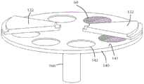
参照图6A至图6E,本公开的一或更多个实施例是关于在其上具有特征310的基板表面300上沉积间隔件膜的处理方法。特征310可以是膜可以沉积于其上的任何三维结构。附图所示的特征310是心轴;然而,本领域技术人员将理解这仅为一种可能结构的代表。适合的特征310包括但不限于脊部、沟槽、及通孔。Referring to FIGS. 6A-6E , one or more embodiments of the present disclosure relate to a process for depositing a spacer film on a
特征310包括顶部320、底部330、及侧壁340。在所示的实施例中,特征310在特征310的任一侧上具有两个侧壁340。特征310具有由顶部320与底部330定义的高度以及由侧壁340之间的距离定义的宽度。
基板表面300在其上提供有至少一个特征310。如在本说明书与随附权利要求中所使用的,以此方式使用的术语“提供”意指基板表面300被放置或定位在用于处理的环境中。The
如图6B所示,在基板表面300上形成膜350,使得膜形成于至少一个特征310上。膜350形成于特征310的顶部320、底部330、及侧壁340上。在一些实施例中,膜350共形地形成于特征310上。如本文所使用的,术语“共形”或“共形地”指称黏附至并均匀地覆盖所暴露表面的层,该层的厚度具有小于相对于膜的平均厚度的1%的变化。举例而言,

在一些实施例中,膜350包含SiN。可以通过任何适合的方法执行SiN的形成,包括但不限于原子层沉积(ALD)、等离子体增强原子层沉积(PEALD)、化学气相沉积(CVD)、及等离子体增强化学气相沉积(PECVD)。在一些实施例中,膜350是通过ALD处理而形成的SiN,其中基板表面300依序暴露于硅前驱物与氮反应物。如此处所使用,“硅前驱物”与基板的表面反应,使得硅分子停留于基板表面上。如此处所使用,“氮反应物”与基板表面上的硅分子反应。In some embodiments,
在一些实施例中,利用在暴露于硅前驱物与氮反应物之间暴露于氮前驱物,来在基板表面300上形成SiN膜。如此处所使用,“氮前驱物”与基板表面反应,且最少地与已存在于基板表面上的硅物种反应。换言之,氮前驱物包含不与基板表面上的硅前驱物分子反应的物种。由于氮前驱物物种与硅前驱物物种都与基板表面反应,且彼此具有最小的反应性,所以暴露于氮前驱物可以发生于暴露于硅前驱物之前、暴露于硅前驱物期间、或暴露于硅前驱物之后。In some embodiments, a SiN film is formed on the
适合的硅前驱物包括但不限于甲硅烷、乙硅烷、二氯硅烷(DCS)、双(二乙氨基)硅烷(BDEAS)、四(二甲氨基)硅烷(TDMAS)、和/或双(叔丁基氨基)硅烷(BTBAS)。在一些实施例中,硅前驱物包含二氯硅烷。在一或更多个实施例中,硅前驱物基本上由二氯硅烷组成,而这意指以原子计存在少于1%的二氯硅烷之外的硅物种。Suitable silicon precursors include, but are not limited to, monosilane, disilane, dichlorosilane (DCS), bis(diethylamino)silane (BDEAS), tetrakis(dimethylamino)silane (TDMAS), and/or bis(tertiary Butylamino)silane (BTBAS). In some embodiments, the silicon precursor includes dichlorosilane. In one or more embodiments, the silicon precursor consists essentially of dichlorosilane, which means that less than 1% by atom of silicon species other than dichlorosilane is present.
适合的氮前驱物包括但不限于分子氮与氨。在氮前驱物暴露期间所采用的处理条件可以影响氮物种与表面上的硅物种的反应性。在一些实施例中,处理条件经配置以使得氮前驱物基本上仅与基板表面反应。如此处所使用,术语“基本上仅”意指氮前驱物与少于约10%的表面硅物种反应。Suitable nitrogen precursors include, but are not limited to, molecular nitrogen and ammonia. The processing conditions employed during nitrogen precursor exposure can affect the reactivity of nitrogen species with silicon species on the surface. In some embodiments, the processing conditions are configured such that the nitrogen precursor reacts substantially only with the substrate surface. As used herein, the term "substantially only" means that the nitrogen precursor reacts with less than about 10% of the surface silicon species.
氮反应物是在基板表面上形成氮化硅膜的物种。在一些实施例中,氮反应物提供用于形成氮化物膜(例如,SiN)的氮原子。在一或更多个实施例中,氮反应物不包括含氮物种,并通过促进表面物种之间的反应而形成氮化物膜。适合的氮反应物包括但不限于氮等离子体、氨等离子体、包含氢、氮、氨、氦、氩、或氧中的两或更多者的混合物的等离子体。在一些实施例中,氮反应物包括氩与氨的等离子体、或氩与氮的等离子体、或氩与氧的等离子体、或氦与氨的等离子体。在一些实施例中,氮反应物包含不含与表面上的氮物种反应的氮的等离子体。在一些实施例中,氮反应物包含氢与氩的等离子体、或氢与氮的等离子体、或氢与氦的等离子体、或氢与氨的等离子体、或氢与氧的等离子体。Nitrogen reactants are species that form a silicon nitride film on the substrate surface. In some embodiments, the nitrogen reactant provides nitrogen atoms for forming a nitride film (eg, SiN). In one or more embodiments, the nitrogen reactant does not include nitrogen-containing species, and forms a nitride film by promoting a reaction between surface species. Suitable nitrogen reactants include, but are not limited to, nitrogen plasmas, ammonia plasmas, plasmas containing mixtures of two or more of hydrogen, nitrogen, ammonia, helium, argon, or oxygen. In some embodiments, the nitrogen reactant includes a plasma of argon and ammonia, or a plasma of argon and nitrogen, or a plasma of argon and oxygen, or a plasma of helium and ammonia. In some embodiments, the nitrogen reactant comprises a plasma free of nitrogen that reacts with nitrogen species on the surface. In some embodiments, the nitrogen reactant comprises a plasma of hydrogen and argon, or a plasma of hydrogen and nitrogen, or a plasma of hydrogen and helium, or a plasma of hydrogen and ammonia, or a plasma of hydrogen and oxygen.
如图6C所示,在形成膜350(例如,氮化硅)之后,利用具有高离子浓度的等离子体360加工膜350。等离子体360可以是定向等离子体。如在本说明书与所附权利要求中所使用的,术语“定向等离子体”是指存在于等离子体中的能量物种(离子与自由基)在特定方向上移动。举例而言,在图6C中,等离子体360图示为向下移动,使得能量物种能够接触顶表面320与底表面330上的膜350,但与侧壁340上的膜350具有最小的接触。As shown in FIG. 6C, after the film 350 (for example, silicon nitride) is formed, the
具有高离子浓度的等离子体具有大于或等于约1010/cm3的浓度。在一或更多个实施例中,具有高离子浓度的等离子体具有大于或等于约109/cm3、1011/cm3、1012/cm3、1013/cm3、或1014/cm3的浓度。A plasma with a high ion concentration has a concentration greater than or equal to about 1010 /cm3 .Inoneor more embodiments, a plasmahavingahighion concentration hasan cm3 concentration.
定向等离子体可以形成为远程等离子体,其中等离子体物种相对于基板表面远程激发,并朝向基板表面流动。基板与基板支撑件可以不是用于产生等离子体的电路径的一部分。定向等离子体亦可以形成为直接等离子体,其中基板或基板支撑件可在等离子体形成中充当电极。直接等离子体通常是扩散等离子体,并可以通过向基板施加偏压而定向,使得离子被吸引到基板并朝向基板移动。Directed plasmas can be formed as remote plasmas, where plasma species are excited remotely relative to the substrate surface and flow towards the substrate surface. The substrate and substrate support may not be part of the electrical path used to generate the plasma. Directed plasmas can also be formed as direct plasmas, where the substrate or substrate support can act as an electrode in the formation of the plasma. Direct plasmas are generally diffuse plasmas and can be oriented by applying a bias to the substrate such that ions are attracted to and move towards the substrate.
如图6D所示,利用具有高离子浓度的等离子体对膜350加工,以修改在顶部320与底部330处的膜350的性质。在一些实施例中,改变膜350的性质以形成经改性的顶部膜352与经改性的底部膜353,而影响稀释HF(1%)中的湿式蚀刻速率,使得可从特征310蚀刻经改性的顶部膜352与经改性的底部膜353,而基本上不影响侧壁膜354。在一些实施例中,该加工损伤特征310的顶部与底部上的膜350,使得可以相对于侧壁选择性地蚀刻膜。As shown in FIG. 6D , the
在一些实施例中,经改性的顶部膜352与经改性的底部膜353的湿式蚀刻速率大于或等于约


用于加工的等离子体可以是能够修改膜性质的任何适合的等离子体(例如,直接的或远程的)。在一些实施例中,加工包含氢、氩、氮、氨、氧、或氦中的一或更多者。The plasma used for processing can be any suitable plasma (eg, direct or remote) capable of modifying film properties. In some embodiments, the process includes one or more of hydrogen, argon, nitrogen, ammonia, oxygen, or helium.
用于加工的时间量可以影响对特征的顶部与底部上的膜所造成的损伤量。等离子体物种与功率可以影响对膜造成的损伤的深度。对膜造成较深损伤的加工处理可以比对膜造成较浅损伤的加工处理重复更少。举例而言,He/NH3等离子体可以造成比Ar/NH3等离子体更深的损伤,使得在利用He/NH3等离子体加工之前,所沉积的膜可以更厚。The amount of time used for processing can affect the amount of damage done to the film on the top and bottom of the feature. Plasma species and power can affect the depth of damage to the film. Processing that causes deeper damage to the membrane can be repeated less often than processing that causes shallower damage to the membrane. For example, He/NH3 plasma can cause deeper damage than Ar/NH3 plasma, so that the deposited film can be thicker before processing with He/NH3 plasma.
可以重复膜350的形成与加工,直到已形成具有预定总厚度的膜。可以依序重复膜形成处理中的每一步骤,以形成用于加工的膜。然后,可以加工该膜,并重复该处理。在一些实施例中,利用等离子体360对膜350加工是发生在沉积具有约


在该方法的一些实施例中,蚀刻膜350。相对于侧壁膜354选择性蚀刻经改性的顶部膜352与经改性的底部膜353。如此处所使用,选择性蚀刻意指顶部与底部上的蚀刻的量、速率、或程度大于侧壁上的蚀刻。在一些实施例中,利用稀释HF对膜蚀刻,以从特征的顶部与底部选择性地移除膜。图6E图示蚀刻处理的结果。尽管附图图示特征310的顶部及底部与侧壁膜354的方角,但是本领域技术人员将理解这仅为说明性的,且边缘与角部并非为完全直的或方的。In some embodiments of the method,
本公开的一些实施例是关于使用批处理腔室(亦称为空间处理腔室)沉积间隔件材料的处理。图1图示处理腔室100的横截面,处理腔室100包括气体分配组件120(亦称为注射器或注射器组件)与基座组件140。气体分配组件120是用于处理腔室中的任何类型的气体递送装置。气体分配组件120包括面向基座组件140的前表面121。前表面121可具有任何数目或种类的开口,以朝向基座组件140传递气体流。气体分配组件120亦包括外边缘124,其在所示实施例中基本上为圆形。Some embodiments of the present disclosure relate to processes for depositing spacer material using batch processing chambers (also known as spatial processing chambers). FIG. 1 illustrates a cross-section of a
所使用的气体分配组件120的具体类型可以取决于正使用的特定处理而变化。本公开的实施例可用于其中控制基座与气体分配组件之间的间隙的任何类型的处理系统。尽管可采用各种类型的气体分配组件(例如,喷淋头),但本公开的实施例利用具有多个基本上平行的气体通道的空间气体分配组件的情况下可以特别有用。如在此说明书及随附权利要求中所使用,术语“基本上平行”意指气体通道的细长轴在大致相同的方向上延伸。在气体通道的平行中可以存在轻微的瑕疵。在二元反应中,多个基本上平行的气体通道可包括至少一个第一反应性气体A通道、至少一个第二反应性气体B通道、至少一个净化气体P通道、和/或至少一个真空V通道。将自第一反应性气体A通道、第二反应性气体B通道、及净化气体P通道流动的气体引导朝向晶片的顶表面。气体流中的一些横跨晶片的表面水平地移动,并通过净化气体P通道水平移动出处理区域。从气体分配组件的一端移动到另一端的基板将轮流暴露于处理气体的每一者,以在基板表面上形成层。The specific type of
在一些实施例中,气体分配组件120是由单一注射器单元制成的刚性固定主体。在一或更多个实施例中,如图2所示,气体分配组件120由多个独立扇区(例如,注射器单元122)组成。单件体或多扇区体皆可用于所描述的本公开的各种实施例。In some embodiments,
基座组件140定位于气体分配组件120下方。基座组件140包括顶表面141以及顶表面141中的至少一个凹部142。基座组件140亦具有底表面143与边缘144。取决于正处理的基板60的形状及大小,凹部142可以是任何合适的形状及大小。在图1所示的实施例中,凹部142具有平坦底部,以支撑晶片的底部;然而,凹部的底部可以变化。在一些实施例中,凹部具有环绕凹部的外周边缘的阶梯区域,阶梯区域可被设定大小以支撑晶片的外周边缘。举例而言,取决于晶片的厚度与晶片背侧上已存在的特征的呈现,由阶梯所支撑的晶片的外周边缘的量可以变化。
在一些实施例中,如图1所示,基座组件140的顶表面141中的凹部142可被设定大小,使得支撑于凹部142中的基板60具有与基座组件140的顶表面141基本上共面的顶表面61。如在此说明书及随附权利要求中所使用,术语“基本上共面”意指晶片的顶表面及基座组件的顶表面是在±0.2mm内共面。在一些实施例中,所述顶表面是在±0.15mm、±0.10mm、或±0.05mm内共面。In some embodiments, as shown in FIG. Coplanar
图1的基座组件140包括能够提起、降低、及旋转基座组件140的支撑柱160。基座组件可包括加热器、或气体管线、或在支撑柱160的中心内的电气部件。支撑柱160可以是增加或减少在基座组件140与气体分配组件120间的间隙的主要构件,以移动基座组件140至合适的位置。基座组件140亦可包括微调谐致动器162,微调谐致动器162可对基座组件140进行微调整,以建立基座组件140与气体分配组件120之间的预定间隙170。The
在一些实施例中,间隙170的距离是在约0.1mm至约5.0mm的范围中、或在约0.1mm至约3.0mm的范围中、或在约0.1mm至约2.0mm的范围中、或在约0.2mm至约1.8mm的范围中、或在约0.3mm至约1.7mm的范围中、或在约0.4mm至约1.6mm的范围中、或在约0.5mm至约1.5mm的范围中、或在约0.6mm至约1.4mm的范围中、或在约0.7mm至约1.3mm的范围中、或在约0.8mm至约1.2mm的范围中、或在约0.9mm至约1.1mm的范围中、或约1mm。In some embodiments, the distance of
附图所示的处理腔室100是转盘型腔室,其中基座组件140可固持多个基板60。如图2所示,气体分配组件120可包括多个分离的注射器单元122,每一注射器单元122能够在晶片于注射器单元下方移动时,在晶片上沉积膜。两个派形注射器单元122图示为位于基座组件140上方的大约相对侧上。此数目的注射器单元122仅用于说明目的而显示。应理解可包括更多或更少注射器单元122。在一些实施例中,有足够数目的派形注射器单元122以形成与基座组件140的形状共形的形状。在一些实施例中,独立派形注射器单元122的每一者可独立地移动、移除和/或置换而不影响其他注射器单元122的任一者。举例而言,可提高一个区段,以允许机器人进出基座组件140与气体分配组件120之间的区域,以装载/卸除基板60。The
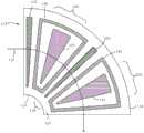
具有多个气体注射器的处理腔室可用以同时处理多个晶片,使得晶片经历相同的处理流程。举例而言,如图3所示,处理腔室100具有四个气体注射器组件与四个基板60。在处理开始时,基板60可定位于注射器组件30之间。以45°旋转17基座组件140将导致气体分配组件120之间的每一基板60移动到气体分配组件120以进行膜沉积,如气体分配组件120下方的虚线圆形所示。额外的45°旋转将让基板60移动远离注射器组件30。基板60与气体分配组件120的数目可以相同或不同。在一些实施例中,正在处理的晶片与气体分配组件具有相同的数目。在一或更多个实施例中,正在处理的晶片的数目是气体分配组件的数目的一小部分或整数倍数。举例而言,若有四个气体分配组件,则有4x个正在处理的晶片,其中x是大于或等于1的整数值。在示例性实施例中,气体分配组件120包括通过气体帘幕分离的八个处理区域,而基座组件140可容纳六个晶片。A processing chamber with multiple gas injectors can be used to process multiple wafers simultaneously such that the wafers undergo the same process flow. For example, as shown in FIG. 3 , the
图3所示的处理腔室100仅为一个可能配置的代表,且不应视为限制本公开的范围。此处,处理腔室100包括多个气体分配组件120。在所示实施例中,具有绕处理腔室100均匀地间隔开的四个气体分配组件(亦称为注射器组件30)。所示处理腔室100是八角形;然而,本该领域技术人员将了解此是一个可能形状,且不应视为限制本公开的范围。所示气体分配组件120是梯形的,但可以是单一圆形部件或由多个派形区段组成,如图2所示。The
图3所示的实施例包括装载锁定腔室180,或辅助腔室,如缓冲站。此腔室180连接至处理腔室100的一侧,以允许例如让基板(亦称为基板60)从腔室100装载/卸除。晶片机器人可位于腔室180中,以将基板移动到基座上。The embodiment shown in FIG. 3 includes a
转盘(例如,基座组件140)的旋转可以是连续的或间歇(不连续)的。在连续处理中,晶片不断地旋转,使得晶片轮流暴露于注射器的每一者。在不连续处理中,可将晶片移动到注射器区域并停止,且接着到注射器之间的区域84并停止。举例而言,转盘可旋转使得晶片从注射器间区域移动而横跨注射器(或相邻于注射器而停止),且接着继续到转盘可再次暂停的下一个注射器间区域。注射器之间的暂停可为每一层沉积之间的额外处理步骤(例如,暴露于等离子体)提供时间。The rotation of the turntable (eg, base assembly 140) may be continuous or intermittent (discontinuous). In continuous processing, the wafer is continuously rotated so that the wafer is exposed to each of the injectors in turn. In discontinuous processing, the wafer may be moved to the injector area and stopped, and then to the
图4图示气体分配组件220的扇区或部分,其可称为注射器单元122。注射器单元122可独立使用或与其他注射器单元组合使用。举例而言,如图5所示,四个图4的注射器单元122经组合以形成单一气体分配组件220。(为了清楚而未显示分离四个注射器的线。)尽管图4的注射器单元122除了净化气体端口155与真空端口145之外亦具有第一反应性气体端口125与第二气体端口135二者,但是注射器单元122不需要所有这些部件。FIG. 4 illustrates a sector or portion of gas distribution assembly 220 , which may be referred to as
参照图4与图5二者,根据一或更多个实施例的气体分配组件220可包含多个扇区(或注射器单元122),且每一扇区是相同的或不同的。气体分配组件220位于处理腔室内,且在气体分配组件220的前表面121中包含多个细长气体端口125、135、145。多个细长气体端口125、135、145、155从相邻于气体分配组件220内周边缘123的区域朝向相邻于气体分配组件220外周边缘124的区域延伸。所示多个气体端口包括第一反应性气体端口125、第二气体端口135、真空端口145、及净化气体端口155,该真空端口145环绕第一反应性气体端口与第二反应性气体端口的每一者。Referring to both Figures 4 and 5, the gas distribution assembly 220 according to one or more embodiments may include multiple sectors (or injector units 122), with each sector being the same or different. A gas distribution assembly 220 is located within the processing chamber and includes a plurality of
然而,参照图4或图5所示的实施例,当叙述端口从至少绕内周区域延伸到至少绕外周区域时,端口可延伸较仅在径向上从内区域至外区域更多。在真空端口145环绕反应性气体端口125与反应性气体端口135时,端口可在切线上延伸。在图4或图5所示的实施例中,楔形反应性气体端口125、135在所有边缘上(包括与内周边缘区域与外周边缘区域相邻处)由真空端口145环绕。However, when referring to the embodiment shown in Figure 4 or Figure 5, when the ports are described as extending from at least around the inner peripheral region to at least around the outer peripheral region, the ports may extend more than just radially from the inner region to the outer region. As the
参照图4,随着基板沿着路径127移动,基板表面的每一部分暴露于各种反应性气体。为了沿着路径127,基板将暴露至(或“看到”)净化气体端口155、真空端口145、第一反应性气体端口125、真空端口145、净化气体端口155、真空端口145、第二气体端口135、及真空端口145。因此,在图4所示的路径127的结束处,基板已暴露至第一反应性气体125与第二反应性气体135以形成层。所示注射器单元122形成四分之一圆,但可更大或更小。图5所示的气体分配组件220可视为串联连接的四个图4的注射器单元122的组合。Referring to FIG. 4, as the substrate moves along
图4的注射器单元122图示分离反应性气体的气体帘幕150。术语“气体帘幕”用于描述任何分离反应性气体以免混合的气体流或真空的组合。图4所示的气体帘幕150包含第一反应性气体端口125旁边的真空端口145的一部分、在中间的净化气体端口155、及第二气体端口135旁边的真空端口145的一部分。气体流及真空的此组合可用以防止或最小化第一反应性气体与第二反应性气体的气相反应。The
参照图5,来自气体分配组件220的气体流及真空的组合形成对多个处理区域250的分离。利用在250之间的气体帘幕150环绕独立气体端口125、135大致限定处理区域。图5所示的实施例构成其间具有八个分离的气体帘幕150的八个分离的处理区域250。处理腔室可具有至少两个处理区域。在一些实施例中,至少具有三、四、五、六、七、八、九、十、十一、或十二个处理区域。Referring to FIG. 5 , the combination of gas flow and vacuum from gas distribution assembly 220 creates separation of
在处理期间,基板可在任何给定时间暴露至一个以上的处理区域250。然而,暴露至不同处理区域的部分将具有分离二者的气体帘幕。举例而言,若基板的前边缘进入包括第二气体端口135的处理区域,则基板之中间部分将在气体帘幕150下方,而基板的后边缘将在包括第一反应性气体端口125的处理区域中。During processing, a substrate may be exposed to more than one
工厂接口280(举例而言,可以是装载锁定腔室)图示为连接至处理腔室100。基板60图示为迭加于气体分配组件220之上,以提供参考框架。基板60通常可坐落于基座组件上,以被固持在气体分配板120的前表面121附近。基板60经由工厂接口280装载进入处理腔室100至基板支撑件或基座组件上(见图3)。基板60可图示为位于处理区域内,因为基板被定位为与第一反应性气体端口125相邻,且在两个气体帘幕150a、150b之间。沿着路径127旋转基板60将使基板以逆时针方向环绕处理腔室100移动。因此,基板60将暴露至第一处理区域250a到第八处理区域250h,并包括之间的所有处理区域。A
本公开的实施例是关于包含处理腔室100的处理方法,处理腔室100具有多个处理区域250a-250h,其中每一处理区域通过气体帘幕150与相邻区域分离。举例而言,图5所图示的处理腔室。取决于气体流的布置,处理腔室中的气体帘幕与处理区域的数目可以是任何适当的数目。图5所示的实施例具有八个气体帘幕150与八个处理区域250a-250h。Embodiments of the present disclosure pertain to processing methods involving a
多个基板60位于基板支撑件上,例如,图1与图2所示的基座组件140。环绕处理区域旋转多个基板60,以用于处理。大体上,在整个处理(包括没有反应性气体流入腔室的期间)中密合(气体流动与真空开启)气体帘幕150。A plurality of
因此,本公开的一或更多个实施例是关于利用如图5所示的批处理腔室的处理方法。将基板60放置于具有多个区段250的处理腔室中,每一区段通过气体帘幕150与相邻区段分离。Accordingly, one or more embodiments of the present disclosure relate to a processing method utilizing a batch processing chamber as shown in FIG. 5 . The
该方法的一些实施例包含将其上具有特征的基板表面暴露于沉积环境以沉积膜。如此处所使用,“沉积环境”包含独立或依序沉积膜的一或更多个处理区域或处理条件。Some embodiments of the method include exposing the surface of the substrate having features thereon to a deposition environment to deposit the film. As used herein, "deposition environment" includes one or more processing regions or processing conditions that independently or sequentially deposit films.
在示例性处理中,基板表面的至少一部分暴露于处理腔室的第一区段250a中的第一处理条件。一些实施例的第一处理条件包含硅前驱物,以形成硅膜。在一或更多个实施例中,第一处理条件包含二氯硅烷。In an exemplary process, at least a portion of the substrate surface is exposed to a first processing condition in a
基板表面横向移动穿过气体帘幕150至第二区段250b。硅层在第二区段250b中暴露于第二处理条件。一些实施例的第二处理条件包含氮前驱物,以形成氮膜。在一或更多个实施例中,第二处理条件包含氨。The substrate surface moves laterally through the
基板表面从第二处理区域横向移动至第三区段250c。一些实施例的第三区段250c包含第三处理条件,该第三处理条件包含在特征的顶部、底部、及侧壁上形成膜的反应物。第四区段250d可以包含惰性环境。在一些实施例中,第三区段250c包括惰性环境,使得基本上不存在表面反应,而第四区段250d包含第三处理条件。在一或更多个实施例中,第三处理条件包含N2/Ar等离子体。The substrate surface is moved laterally from the second processing region to the
可以重复暴露于第一处理条件、第二处理条件、及第三处理条件,以形成具有预定厚度的膜。举例而言,参照图5,第一区段250a与第五区段250e可包含第一处理条件;第二区段250b与第六区段250f可包含第二处理条件;第三区段250c与第七区段250g可包含惰性环境;以及第四区段250d与第八区段250h可包含第三处理条件。在此布置中,基板的每一旋转形成两个层。本领域技术人员将理解,使用例如“第一”与“第二”之类的序数描述处理区域并非暗示处理腔室内的具体位置或处理腔室内的暴露顺序。The exposure to the first processing condition, the second processing condition, and the third processing condition may be repeated to form a film having a predetermined thickness. For example, referring to FIG. 5, the
一旦已形成预定厚度的层,第一处理条件、第二处理条件、及第三处理条件可以改变成惰性环境。举例而言,第三区段250c中的惰性环境可以改变成包含高离子浓度等离子体的加工环境,以选择性降低特征的顶部与底部上的氮化硅膜的湿式蚀刻速率。举例而言,高离子浓度等离子体可包含He/NH3。在暴露于加工环境之后,处理腔室的独立区段可以改变回到先前的设定,或者可停止该处理。Once a layer of predetermined thickness has been formed, the first processing condition, the second processing condition, and the third processing condition may be changed to an inert environment. For example, the inert environment in the
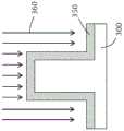
参照图7,一些实施例使用具有狭槽382的等离子体组件380。等离子体形成于等离子体空腔384中,并通过狭槽382朝向基板表面300流动。图7所示的视图为横截面图,其中狭槽382延伸到页面外。形成于等离子体空腔384中的等离子体流经的狭槽382具有边缘386。在一些实施例中,等离子体在相邻于狭槽382的边缘386处具有高离子能量与浓度。Referring to FIG. 7 , some embodiments use a plasma assembly 380 with a
根据一或更多个实施例,基板在形成层之前和/或之后经受处理。此处理可在相同腔室中执行,或在一或更多个分离的处理腔室中执行。在一些实施例中,将基板从第一腔室移动至分离的第二腔室,以用于进一步处理。基板可从第一腔室直接移动至分离的处理腔室,或者可从第一腔室移动至一或更多个转移腔室,且接着移动到分离的处理腔室。因此,处理设备可包含与转移站连通的多个腔室。此种类的设备可称为“群集工具”或“群集系统”及类似者。According to one or more embodiments, the substrate is subjected to processing before and/or after forming the layers. This processing can be performed in the same chamber, or in one or more separate processing chambers. In some embodiments, the substrate is moved from the first chamber to a separate second chamber for further processing. The substrate may be moved directly from the first chamber to a separate processing chamber, or may be moved from the first chamber to one or more transfer chambers and then to a separate processing chamber. Thus, a processing apparatus may comprise a plurality of chambers in communication with a transfer station. Devices of this kind may be called "cluster tools" or "cluster systems" and the like.
一般而言,群集工具是模块化系统,该模块化系统包含执行多种功能的多个腔室,该等功能包括基板的定心及定向、退火、退火、沉积、和/或蚀刻。根据一或更多个实施例,群集工具至少包括第一腔室与中央转移腔室。中央转移腔室可容纳机器人,该机器人可在处理腔室及装载锁定腔室之间梭运基板。转移腔室通常维持在真空条件下,并提供中继阶段,该中继阶段用于从一个腔室梭运基板至位于群集工具的前端的另一腔室和/或装载锁定腔室。可适配用于本公开的两个已知群集工具是

根据一或更多个实施例,基板是连续地在真空下或“装载锁定”条件下,且在从一个腔室移动到下一腔室时不暴露至周围空气。因此,转移腔室是在真空下,且“泵降”至真空压力下。惰性气体可存在于处理腔室或转移腔室中。在一些实施例中,惰性气体是作为净化气体,以移除一些或全部的反应物。根据一或更多个实施例,将净化气体注入于沉积腔室的出口处,用以避免反应物从沉积腔室移动至转移腔室和/或额外的处理腔室。因此,惰性气体流在腔室的出口处形成帘幕。According to one or more embodiments, the substrates are continuously under vacuum or "load lock" conditions and are not exposed to ambient air while moving from one chamber to the next. Thus, the transfer chamber is under vacuum and "pumped down" to vacuum pressure. An inert gas may be present in the processing chamber or the transfer chamber. In some embodiments, an inert gas is used as a purge gas to remove some or all of the reactants. According to one or more embodiments, a purge gas is injected at the outlet of the deposition chamber to avoid migration of reactants from the deposition chamber to the transfer chamber and/or additional processing chambers. Thus, the flow of inert gas forms a curtain at the outlet of the chamber.
可在单一基板沉积腔室中处理基板,其中在处理另一基板之前装载、处理、及卸除单一基板。亦可利用类似于输送系统的连续方式处理基板,其中将多个基板独立装载至腔室的第一部分中,移动穿过腔室,并且从腔室的第二部分卸除。腔室和相关联的输送器系统的形状可以形成直线路径或弯曲路径。此外,处理腔室可以是转盘,其中多个基板绕中心轴线移动,并暴露于整个转盘路径的沉积、蚀刻、退火、清洗等的处理。Substrates can be processed in a single substrate deposition chamber, where a single substrate is loaded, processed, and unloaded before another substrate is processed. Substrates may also be processed in a continuous manner similar to a conveyor system, where multiple substrates are independently loaded into a first portion of the chamber, moved through the chamber, and unloaded from a second portion of the chamber. The shape of the chamber and associated conveyor system can form a straight path or a curved path. Additionally, the processing chamber may be a carousel where multiple substrates are moved about a central axis and exposed to processes of deposition, etching, annealing, cleaning, etc. throughout the path of the carousel.
在处理期间,基板可被加热或冷却。此类加热或冷却可通过任何合适的手段达成,包括但不限于改变基板支撑件的温度、及使经加热或经冷却的气体流动至基板表面。在一些实施例中,基板支撑件包括加热器/冷却器,该加热器/冷却器可经控制用以利用传导方式改变基板温度。在一或更多个实施例中,所采用的气体(反应性气体或惰性气体)被加热或冷却以局部改变基板温度。在一些实施例中,加热器/冷却器位于腔室内且邻近于基板表面,以对流地改变基板温度。During processing, the substrate may be heated or cooled. Such heating or cooling may be accomplished by any suitable means, including, but not limited to, changing the temperature of the substrate support, and flowing heated or cooled gas to the substrate surface. In some embodiments, the substrate support includes a heater/cooler that is controllable to vary the temperature of the substrate using conduction. In one or more embodiments, the gas employed (reactive or inert) is heated or cooled to locally vary the substrate temperature. In some embodiments, a heater/cooler is located within the chamber adjacent to the substrate surface to convectively vary the substrate temperature.
基板在处理期间亦可静止或旋转。旋转的基板可连续地或以离散步进方式旋转。举例而言,基板可在整个处理过程中旋转,或基板可在暴露于不同反应性气体或净化气体之间少量旋转。在处理期间旋转基板(连续地或步进式)可以有助于通过最小化例如气体流几何中的局部可变性的效应,而产生更均匀的沉积或蚀刻。The substrate may also be stationary or rotated during processing. The rotating substrate can be rotated continuously or in discrete steps. For example, the substrate may be rotated throughout processing, or the substrate may be rotated in small amounts between exposure to different reactive or purge gases. Rotating the substrate (continuously or stepwise) during processing can help produce more uniform deposition or etching by minimizing effects such as local variability in gas flow geometry.
在原子层沉积型腔室中,基板可以在空间或时间上分离的处理中暴露于第一与第二前驱物。时间ALD为传统处理,其中第一前驱物流入腔室中而与表面反应。在流动第二前驱物之前,从腔室净化第一前驱物。在空间ALD中,第一与第二前驱物两者同时流至腔室,但在空间上分离,使得在流动之间存在防止前驱物混合的区域。在空间ALD中,基板相对于气体分配板移动,或反之亦然。In an atomic layer deposition type chamber, a substrate may be exposed to first and second precursors in spatially or temporally separated processes. Temporal ALD is a traditional process in which a first precursor flows into a chamber to react with the surface. The first precursor is purged from the chamber prior to flowing the second precursor. In space ALD, both the first and second precursors flow to the chamber simultaneously, but are spatially separated such that there is an area between the flows that prevents mixing of the precursors. In spatial ALD, the substrate moves relative to the gas distribution plate, or vice versa.
在该等方法的一或更多个部分在一个腔室中进行的实施例中,该方法可以是空间ALD处理。尽管上述化学物质中的一或更多种可能不兼容(即,导致基板表面上和/或腔室上沉积之外的反应),但空间分离确保试剂不暴露于气相中的每一者。举例而言,时间ALD涉及净化沉积腔室。然而,在实施中,有时候不可能在额外试剂流入之前将过量试剂从腔室中净化掉。因此,腔室中的任何剩余试剂可能反应。利用空间分离,不需要净化过量试剂,并使交叉污染受到限制。此外,由于净化腔室会使用大量时间,因此通过消除净化步骤可以增加产量。In embodiments where one or more portions of the methods are performed in one chamber, the method may be a spatial ALD process. While one or more of the aforementioned chemistries may be incompatible (ie, cause reactions other than deposition on the substrate surface and/or on the chamber), the spatial separation ensures that the reagents are not exposed to each in the gas phase. For example, temporal ALD involves purging the deposition chamber. However, in practice, it is sometimes not possible to purge excess reagent from the chamber before additional reagent flows in. Therefore, any remaining reagents in the chamber may react. With spatial separation, purification of excess reagents is not required and cross-contamination is limited. Also, since the purge chamber uses a significant amount of time, throughput can be increased by eliminating the purge step.
整个本说明书引用“一个实施例”、“某些实施例”、“一或更多个实施例”、或“实施例”意指结合实施例描述的特定特征、结构、材料、或特性被包括在本公开的至少一个实施例中。因此,整个本说明书的各处出现的如“在一或更多个实施例中”、“在某些实施例中”、“在一个实施例中”、或“在实施例中”的短语不一定指称本公开的相同实施例。此外,在一或更多个实施例中,特定特征、结构、材料、或特性可以利用任何合适的方式组合。Reference throughout this specification to "one embodiment," "certain embodiments," "one or more embodiments," or "an embodiment" means that a particular feature, structure, material, or characteristic described in connection with the embodiment is included In at least one embodiment of the present disclosure. Thus, appearances of phrases such as "in one or more embodiments," "in certain embodiments," "in one embodiment," or "in an embodiment" throughout this specification are not Must refer to the same embodiment of the present disclosure. Furthermore, the particular features, structures, materials, or characteristics may be combined in any suitable manner in one or more embodiments.
尽管已参照特定实施例而描述本公开,但应理解,这些实施例仅为本公开的原理与应用的说明。本领域技术人员将理解,在不悖离本公开的精神与范围的情况下,可以对本公开的方法与设备进行各种修改及变化。因此,本公开意欲包括在随附权利要求及其等同物的范围内的修改及变化。Although the disclosure has been described with reference to specific embodiments, it should be understood that these embodiments are merely illustrative of the principles and applications of the disclosure. Those skilled in the art will appreciate that various modifications and changes can be made to the methods and apparatus of the present disclosure without departing from the spirit and scope of the present disclosure. Thus, it is intended that the present disclosure includes modifications and variations within the scope of the appended claims and their equivalents.
Claims (19)


Applications Claiming Priority (3)
| Application Number | Priority Date | Filing Date | Title |
|---|---|---|---|
| US201662307537P | 2016-03-13 | 2016-03-13 | |
| US62/307,537 | 2016-03-13 | ||
| PCT/US2017/021852WO2017160647A1 (en) | 2016-03-13 | 2017-03-10 | Selective deposition of silicon nitride films for spacer applications |
Publications (2)
| Publication Number | Publication Date |
|---|---|
| CN108780735A CN108780735A (en) | 2018-11-09 |
| CN108780735Btrue CN108780735B (en) | 2023-04-21 |
Family
ID=59787037
Family Applications (1)
| Application Number | Title | Priority Date | Filing Date |
|---|---|---|---|
| CN201780015644.XAActiveCN108780735B (en) | 2016-03-13 | 2017-03-10 | Selective Deposition of Silicon Nitride Films for Spacer Applications |
Country Status (6)
| Country | Link |
|---|---|
| US (1) | US10319583B2 (en) |
| JP (1) | JP6946320B2 (en) |
| KR (1) | KR102293218B1 (en) |
| CN (1) | CN108780735B (en) |
| TW (1) | TWI722132B (en) |
| WO (1) | WO2017160647A1 (en) |
Families Citing this family (369)
| Publication number | Priority date | Publication date | Assignee | Title |
|---|---|---|---|---|
| US10378106B2 (en) | 2008-11-14 | 2019-08-13 | Asm Ip Holding B.V. | Method of forming insulation film by modified PEALD |
| US9394608B2 (en) | 2009-04-06 | 2016-07-19 | Asm America, Inc. | Semiconductor processing reactor and components thereof |
| US8802201B2 (en) | 2009-08-14 | 2014-08-12 | Asm America, Inc. | Systems and methods for thin-film deposition of metal oxides using excited nitrogen-oxygen species |
| US9257274B2 (en) | 2010-04-15 | 2016-02-09 | Lam Research Corporation | Gapfill of variable aspect ratio features with a composite PEALD and PECVD method |
| US9312155B2 (en) | 2011-06-06 | 2016-04-12 | Asm Japan K.K. | High-throughput semiconductor-processing apparatus equipped with multiple dual-chamber modules |
| US10364496B2 (en) | 2011-06-27 | 2019-07-30 | Asm Ip Holding B.V. | Dual section module having shared and unshared mass flow controllers |
| US10854498B2 (en) | 2011-07-15 | 2020-12-01 | Asm Ip Holding B.V. | Wafer-supporting device and method for producing same |
| US20130023129A1 (en) | 2011-07-20 | 2013-01-24 | Asm America, Inc. | Pressure transmitter for a semiconductor processing environment |
| US9017481B1 (en) | 2011-10-28 | 2015-04-28 | Asm America, Inc. | Process feed management for semiconductor substrate processing |
| US9659799B2 (en) | 2012-08-28 | 2017-05-23 | Asm Ip Holding B.V. | Systems and methods for dynamic semiconductor process scheduling |
| US10714315B2 (en) | 2012-10-12 | 2020-07-14 | Asm Ip Holdings B.V. | Semiconductor reaction chamber showerhead |
| US20160376700A1 (en) | 2013-02-01 | 2016-12-29 | Asm Ip Holding B.V. | System for treatment of deposition reactor |
| US9484191B2 (en) | 2013-03-08 | 2016-11-01 | Asm Ip Holding B.V. | Pulsed remote plasma method and system |
| US9589770B2 (en) | 2013-03-08 | 2017-03-07 | Asm Ip Holding B.V. | Method and systems for in-situ formation of intermediate reactive species |
| US9240412B2 (en) | 2013-09-27 | 2016-01-19 | Asm Ip Holding B.V. | Semiconductor structure and device and methods of forming same using selective epitaxial process |
| US10683571B2 (en) | 2014-02-25 | 2020-06-16 | Asm Ip Holding B.V. | Gas supply manifold and method of supplying gases to chamber using same |
| US10167557B2 (en) | 2014-03-18 | 2019-01-01 | Asm Ip Holding B.V. | Gas distribution system, reactor including the system, and methods of using the same |
| US11015245B2 (en) | 2014-03-19 | 2021-05-25 | Asm Ip Holding B.V. | Gas-phase reactor and system having exhaust plenum and components thereof |
| US10858737B2 (en) | 2014-07-28 | 2020-12-08 | Asm Ip Holding B.V. | Showerhead assembly and components thereof |
| US9890456B2 (en) | 2014-08-21 | 2018-02-13 | Asm Ip Holding B.V. | Method and system for in situ formation of gas-phase compounds |
| US9657845B2 (en) | 2014-10-07 | 2017-05-23 | Asm Ip Holding B.V. | Variable conductance gas distribution apparatus and method |
| US10941490B2 (en) | 2014-10-07 | 2021-03-09 | Asm Ip Holding B.V. | Multiple temperature range susceptor, assembly, reactor and system including the susceptor, and methods of using the same |
| KR102263121B1 (en) | 2014-12-22 | 2021-06-09 | 에이에스엠 아이피 홀딩 비.브이. | Semiconductor device and manufacuring method thereof |
| US10529542B2 (en) | 2015-03-11 | 2020-01-07 | Asm Ip Holdings B.V. | Cross-flow reactor and method |
| US10276355B2 (en) | 2015-03-12 | 2019-04-30 | Asm Ip Holding B.V. | Multi-zone reactor, system including the reactor, and method of using the same |
| US10458018B2 (en) | 2015-06-26 | 2019-10-29 | Asm Ip Holding B.V. | Structures including metal carbide material, devices including the structures, and methods of forming same |
| US10600673B2 (en) | 2015-07-07 | 2020-03-24 | Asm Ip Holding B.V. | Magnetic susceptor to baseplate seal |
| US9960072B2 (en) | 2015-09-29 | 2018-05-01 | Asm Ip Holding B.V. | Variable adjustment for precise matching of multiple chamber cavity housings |
| US10211308B2 (en) | 2015-10-21 | 2019-02-19 | Asm Ip Holding B.V. | NbMC layers |
| US10322384B2 (en) | 2015-11-09 | 2019-06-18 | Asm Ip Holding B.V. | Counter flow mixer for process chamber |
| US11139308B2 (en) | 2015-12-29 | 2021-10-05 | Asm Ip Holding B.V. | Atomic layer deposition of III-V compounds to form V-NAND devices |
| US20170218517A1 (en)* | 2016-02-01 | 2017-08-03 | Tokyo Electron Limited | Method of forming nitride film |
| JP6548586B2 (en) | 2016-02-03 | 2019-07-24 | 東京エレクトロン株式会社 | Deposition method |
| US10468251B2 (en) | 2016-02-19 | 2019-11-05 | Asm Ip Holding B.V. | Method for forming spacers using silicon nitride film for spacer-defined multiple patterning |
| US10529554B2 (en) | 2016-02-19 | 2020-01-07 | Asm Ip Holding B.V. | Method for forming silicon nitride film selectively on sidewalls or flat surfaces of trenches |
| JP6584347B2 (en)* | 2016-03-02 | 2019-10-02 | 東京エレクトロン株式会社 | Deposition method |
| US10501866B2 (en) | 2016-03-09 | 2019-12-10 | Asm Ip Holding B.V. | Gas distribution apparatus for improved film uniformity in an epitaxial system |
| US10343920B2 (en) | 2016-03-18 | 2019-07-09 | Asm Ip Holding B.V. | Aligned carbon nanotubes |
| US9892913B2 (en) | 2016-03-24 | 2018-02-13 | Asm Ip Holding B.V. | Radial and thickness control via biased multi-port injection settings |
| US10865475B2 (en) | 2016-04-21 | 2020-12-15 | Asm Ip Holding B.V. | Deposition of metal borides and silicides |
| US10190213B2 (en) | 2016-04-21 | 2019-01-29 | Asm Ip Holding B.V. | Deposition of metal borides |
| US10367080B2 (en) | 2016-05-02 | 2019-07-30 | Asm Ip Holding B.V. | Method of forming a germanium oxynitride film |
| US10032628B2 (en) | 2016-05-02 | 2018-07-24 | Asm Ip Holding B.V. | Source/drain performance through conformal solid state doping |
| KR102592471B1 (en) | 2016-05-17 | 2023-10-20 | 에이에스엠 아이피 홀딩 비.브이. | Method of forming metal interconnection and method of fabricating semiconductor device using the same |
| US11453943B2 (en) | 2016-05-25 | 2022-09-27 | Asm Ip Holding B.V. | Method for forming carbon-containing silicon/metal oxide or nitride film by ALD using silicon precursor and hydrocarbon precursor |
| US10388509B2 (en) | 2016-06-28 | 2019-08-20 | Asm Ip Holding B.V. | Formation of epitaxial layers via dislocation filtering |
| US9859151B1 (en) | 2016-07-08 | 2018-01-02 | Asm Ip Holding B.V. | Selective film deposition method to form air gaps |
| US10612137B2 (en) | 2016-07-08 | 2020-04-07 | Asm Ip Holdings B.V. | Organic reactants for atomic layer deposition |
| US10714385B2 (en) | 2016-07-19 | 2020-07-14 | Asm Ip Holding B.V. | Selective deposition of tungsten |
| KR102354490B1 (en) | 2016-07-27 | 2022-01-21 | 에이에스엠 아이피 홀딩 비.브이. | Method of processing a substrate |
| KR102532607B1 (en) | 2016-07-28 | 2023-05-15 | 에이에스엠 아이피 홀딩 비.브이. | Substrate processing apparatus and method of operating the same |
| US10395919B2 (en) | 2016-07-28 | 2019-08-27 | Asm Ip Holding B.V. | Method and apparatus for filling a gap |
| US9812320B1 (en) | 2016-07-28 | 2017-11-07 | Asm Ip Holding B.V. | Method and apparatus for filling a gap |
| US9887082B1 (en) | 2016-07-28 | 2018-02-06 | Asm Ip Holding B.V. | Method and apparatus for filling a gap |
| KR102613349B1 (en) | 2016-08-25 | 2023-12-14 | 에이에스엠 아이피 홀딩 비.브이. | Exhaust apparatus and substrate processing apparatus and thin film fabricating method using the same |
| US10410943B2 (en) | 2016-10-13 | 2019-09-10 | Asm Ip Holding B.V. | Method for passivating a surface of a semiconductor and related systems |
| US10643826B2 (en) | 2016-10-26 | 2020-05-05 | Asm Ip Holdings B.V. | Methods for thermally calibrating reaction chambers |
| US11532757B2 (en) | 2016-10-27 | 2022-12-20 | Asm Ip Holding B.V. | Deposition of charge trapping layers |
| US10643904B2 (en) | 2016-11-01 | 2020-05-05 | Asm Ip Holdings B.V. | Methods for forming a semiconductor device and related semiconductor device structures |
| US10229833B2 (en) | 2016-11-01 | 2019-03-12 | Asm Ip Holding B.V. | Methods for forming a transition metal nitride film on a substrate by atomic layer deposition and related semiconductor device structures |
| US10435790B2 (en) | 2016-11-01 | 2019-10-08 | Asm Ip Holding B.V. | Method of subatmospheric plasma-enhanced ALD using capacitively coupled electrodes with narrow gap |
| US10714350B2 (en) | 2016-11-01 | 2020-07-14 | ASM IP Holdings, B.V. | Methods for forming a transition metal niobium nitride film on a substrate by atomic layer deposition and related semiconductor device structures |
| US10134757B2 (en)* | 2016-11-07 | 2018-11-20 | Asm Ip Holding B.V. | Method of processing a substrate and a device manufactured by using the method |
| KR102546317B1 (en) | 2016-11-15 | 2023-06-21 | 에이에스엠 아이피 홀딩 비.브이. | Gas supply unit and substrate processing apparatus including the same |
| JP6733516B2 (en) | 2016-11-21 | 2020-08-05 | 東京エレクトロン株式会社 | Method of manufacturing semiconductor device |
| US10340135B2 (en) | 2016-11-28 | 2019-07-02 | Asm Ip Holding B.V. | Method of topologically restricted plasma-enhanced cyclic deposition of silicon or metal nitride |
| KR102762543B1 (en) | 2016-12-14 | 2025-02-05 | 에이에스엠 아이피 홀딩 비.브이. | Substrate processing apparatus |
| US11581186B2 (en) | 2016-12-15 | 2023-02-14 | Asm Ip Holding B.V. | Sequential infiltration synthesis apparatus |
| US11447861B2 (en) | 2016-12-15 | 2022-09-20 | Asm Ip Holding B.V. | Sequential infiltration synthesis apparatus and a method of forming a patterned structure |
| KR102700194B1 (en) | 2016-12-19 | 2024-08-28 | 에이에스엠 아이피 홀딩 비.브이. | Substrate processing apparatus |
| US10269558B2 (en) | 2016-12-22 | 2019-04-23 | Asm Ip Holding B.V. | Method of forming a structure on a substrate |
| US10867788B2 (en) | 2016-12-28 | 2020-12-15 | Asm Ip Holding B.V. | Method of forming a structure on a substrate |
| US11390950B2 (en) | 2017-01-10 | 2022-07-19 | Asm Ip Holding B.V. | Reactor system and method to reduce residue buildup during a film deposition process |
| US10655221B2 (en) | 2017-02-09 | 2020-05-19 | Asm Ip Holding B.V. | Method for depositing oxide film by thermal ALD and PEALD |
| US10468261B2 (en) | 2017-02-15 | 2019-11-05 | Asm Ip Holding B.V. | Methods for forming a metallic film on a substrate by cyclical deposition and related semiconductor device structures |
| US10283353B2 (en) | 2017-03-29 | 2019-05-07 | Asm Ip Holding B.V. | Method of reforming insulating film deposited on substrate with recess pattern |
| US10529563B2 (en) | 2017-03-29 | 2020-01-07 | Asm Ip Holdings B.V. | Method for forming doped metal oxide films on a substrate by cyclical deposition and related semiconductor device structures |
| KR102457289B1 (en) | 2017-04-25 | 2022-10-21 | 에이에스엠 아이피 홀딩 비.브이. | Method for depositing a thin film and manufacturing a semiconductor device |
| US10770286B2 (en) | 2017-05-08 | 2020-09-08 | Asm Ip Holdings B.V. | Methods for selectively forming a silicon nitride film on a substrate and related semiconductor device structures |
| US10446393B2 (en) | 2017-05-08 | 2019-10-15 | Asm Ip Holding B.V. | Methods for forming silicon-containing epitaxial layers and related semiconductor device structures |
| US10892156B2 (en) | 2017-05-08 | 2021-01-12 | Asm Ip Holding B.V. | Methods for forming a silicon nitride film on a substrate and related semiconductor device structures |
| US10504742B2 (en) | 2017-05-31 | 2019-12-10 | Asm Ip Holding B.V. | Method of atomic layer etching using hydrogen plasma |
| US10886123B2 (en) | 2017-06-02 | 2021-01-05 | Asm Ip Holding B.V. | Methods for forming low temperature semiconductor layers and related semiconductor device structures |
| US12040200B2 (en) | 2017-06-20 | 2024-07-16 | Asm Ip Holding B.V. | Semiconductor processing apparatus and methods for calibrating a semiconductor processing apparatus |
| US11306395B2 (en) | 2017-06-28 | 2022-04-19 | Asm Ip Holding B.V. | Methods for depositing a transition metal nitride film on a substrate by atomic layer deposition and related deposition apparatus |
| US10685834B2 (en) | 2017-07-05 | 2020-06-16 | Asm Ip Holdings B.V. | Methods for forming a silicon germanium tin layer and related semiconductor device structures |
| KR20190009245A (en) | 2017-07-18 | 2019-01-28 | 에이에스엠 아이피 홀딩 비.브이. | Methods for forming a semiconductor device structure and related semiconductor device structures |
| US11018002B2 (en) | 2017-07-19 | 2021-05-25 | Asm Ip Holding B.V. | Method for selectively depositing a Group IV semiconductor and related semiconductor device structures |
| US10541333B2 (en) | 2017-07-19 | 2020-01-21 | Asm Ip Holding B.V. | Method for depositing a group IV semiconductor and related semiconductor device structures |
| US11374112B2 (en) | 2017-07-19 | 2022-06-28 | Asm Ip Holding B.V. | Method for depositing a group IV semiconductor and related semiconductor device structures |
| US10312055B2 (en) | 2017-07-26 | 2019-06-04 | Asm Ip Holding B.V. | Method of depositing film by PEALD using negative bias |
| US10590535B2 (en) | 2017-07-26 | 2020-03-17 | Asm Ip Holdings B.V. | Chemical treatment, deposition and/or infiltration apparatus and method for using the same |
| US10605530B2 (en) | 2017-07-26 | 2020-03-31 | Asm Ip Holding B.V. | Assembly of a liner and a flange for a vertical furnace as well as the liner and the vertical furnace |
| TWI815813B (en) | 2017-08-04 | 2023-09-21 | 荷蘭商Asm智慧財產控股公司 | Showerhead assembly for distributing a gas within a reaction chamber |
| US10692741B2 (en) | 2017-08-08 | 2020-06-23 | Asm Ip Holdings B.V. | Radiation shield |
| US10770336B2 (en) | 2017-08-08 | 2020-09-08 | Asm Ip Holding B.V. | Substrate lift mechanism and reactor including same |
| US11769682B2 (en) | 2017-08-09 | 2023-09-26 | Asm Ip Holding B.V. | Storage apparatus for storing cassettes for substrates and processing apparatus equipped therewith |
| US10249524B2 (en) | 2017-08-09 | 2019-04-02 | Asm Ip Holding B.V. | Cassette holder assembly for a substrate cassette and holding member for use in such assembly |
| US11139191B2 (en) | 2017-08-09 | 2021-10-05 | Asm Ip Holding B.V. | Storage apparatus for storing cassettes for substrates and processing apparatus equipped therewith |
| US10763108B2 (en)* | 2017-08-18 | 2020-09-01 | Lam Research Corporation | Geometrically selective deposition of a dielectric film |
| USD900036S1 (en) | 2017-08-24 | 2020-10-27 | Asm Ip Holding B.V. | Heater electrical connector and adapter |
| US11830730B2 (en) | 2017-08-29 | 2023-11-28 | Asm Ip Holding B.V. | Layer forming method and apparatus |
| US11056344B2 (en) | 2017-08-30 | 2021-07-06 | Asm Ip Holding B.V. | Layer forming method |
| KR102491945B1 (en) | 2017-08-30 | 2023-01-26 | 에이에스엠 아이피 홀딩 비.브이. | Substrate processing apparatus |
| US11295980B2 (en) | 2017-08-30 | 2022-04-05 | Asm Ip Holding B.V. | Methods for depositing a molybdenum metal film over a dielectric surface of a substrate by a cyclical deposition process and related semiconductor device structures |
| KR102401446B1 (en) | 2017-08-31 | 2022-05-24 | 에이에스엠 아이피 홀딩 비.브이. | Substrate processing apparatus |
| US10607895B2 (en) | 2017-09-18 | 2020-03-31 | Asm Ip Holdings B.V. | Method for forming a semiconductor device structure comprising a gate fill metal |
| KR102630301B1 (en) | 2017-09-21 | 2024-01-29 | 에이에스엠 아이피 홀딩 비.브이. | Method of sequential infiltration synthesis treatment of infiltrateable material and structures and devices formed using same |
| US10844484B2 (en) | 2017-09-22 | 2020-11-24 | Asm Ip Holding B.V. | Apparatus for dispensing a vapor phase reactant to a reaction chamber and related methods |
| US10658205B2 (en) | 2017-09-28 | 2020-05-19 | Asm Ip Holdings B.V. | Chemical dispensing apparatus and methods for dispensing a chemical to a reaction chamber |
| US10403504B2 (en) | 2017-10-05 | 2019-09-03 | Asm Ip Holding B.V. | Method for selectively depositing a metallic film on a substrate |
| US10319588B2 (en) | 2017-10-10 | 2019-06-11 | Asm Ip Holding B.V. | Method for depositing a metal chalcogenide on a substrate by cyclical deposition |
| US10923344B2 (en) | 2017-10-30 | 2021-02-16 | Asm Ip Holding B.V. | Methods for forming a semiconductor structure and related semiconductor structures |
| KR102443047B1 (en) | 2017-11-16 | 2022-09-14 | 에이에스엠 아이피 홀딩 비.브이. | Method of processing a substrate and a device manufactured by the same |
| US10910262B2 (en) | 2017-11-16 | 2021-02-02 | Asm Ip Holding B.V. | Method of selectively depositing a capping layer structure on a semiconductor device structure |
| US11022879B2 (en) | 2017-11-24 | 2021-06-01 | Asm Ip Holding B.V. | Method of forming an enhanced unexposed photoresist layer |
| CN111344522B (en) | 2017-11-27 | 2022-04-12 | 阿斯莫Ip控股公司 | Including clean mini-environment device |
| WO2019103613A1 (en) | 2017-11-27 | 2019-05-31 | Asm Ip Holding B.V. | A storage device for storing wafer cassettes for use with a batch furnace |
| US10290508B1 (en) | 2017-12-05 | 2019-05-14 | Asm Ip Holding B.V. | Method for forming vertical spacers for spacer-defined patterning |
| TWI793218B (en)* | 2017-12-16 | 2023-02-21 | 美商應用材料股份有限公司 | Processing chamber and method for geometrically selective deposition of dielectric films utilizing low frequency bias |
| US10872771B2 (en) | 2018-01-16 | 2020-12-22 | Asm Ip Holding B. V. | Method for depositing a material film on a substrate within a reaction chamber by a cyclical deposition process and related device structures |
| TWI799494B (en) | 2018-01-19 | 2023-04-21 | 荷蘭商Asm 智慧財產控股公司 | Deposition method |
| KR102695659B1 (en) | 2018-01-19 | 2024-08-14 | 에이에스엠 아이피 홀딩 비.브이. | Method for depositing a gap filling layer by plasma assisted deposition |
| USD903477S1 (en) | 2018-01-24 | 2020-12-01 | Asm Ip Holdings B.V. | Metal clamp |
| US11018047B2 (en) | 2018-01-25 | 2021-05-25 | Asm Ip Holding B.V. | Hybrid lift pin |
| USD880437S1 (en) | 2018-02-01 | 2020-04-07 | Asm Ip Holding B.V. | Gas supply plate for semiconductor manufacturing apparatus |
| US10535516B2 (en) | 2018-02-01 | 2020-01-14 | Asm Ip Holdings B.V. | Method for depositing a semiconductor structure on a surface of a substrate and related semiconductor structures |
| US11081345B2 (en) | 2018-02-06 | 2021-08-03 | Asm Ip Holding B.V. | Method of post-deposition treatment for silicon oxide film |
| WO2019158960A1 (en) | 2018-02-14 | 2019-08-22 | Asm Ip Holding B.V. | A method for depositing a ruthenium-containing film on a substrate by a cyclical deposition process |
| US10896820B2 (en) | 2018-02-14 | 2021-01-19 | Asm Ip Holding B.V. | Method for depositing a ruthenium-containing film on a substrate by a cyclical deposition process |
| US10731249B2 (en) | 2018-02-15 | 2020-08-04 | Asm Ip Holding B.V. | Method of forming a transition metal containing film on a substrate by a cyclical deposition process, a method for supplying a transition metal halide compound to a reaction chamber, and related vapor deposition apparatus |
| KR102636427B1 (en) | 2018-02-20 | 2024-02-13 | 에이에스엠 아이피 홀딩 비.브이. | Substrate processing method and apparatus |
| US10658181B2 (en) | 2018-02-20 | 2020-05-19 | Asm Ip Holding B.V. | Method of spacer-defined direct patterning in semiconductor fabrication |
| US10975470B2 (en) | 2018-02-23 | 2021-04-13 | Asm Ip Holding B.V. | Apparatus for detecting or monitoring for a chemical precursor in a high temperature environment |
| US11473195B2 (en) | 2018-03-01 | 2022-10-18 | Asm Ip Holding B.V. | Semiconductor processing apparatus and a method for processing a substrate |
| US11629406B2 (en) | 2018-03-09 | 2023-04-18 | Asm Ip Holding B.V. | Semiconductor processing apparatus comprising one or more pyrometers for measuring a temperature of a substrate during transfer of the substrate |
| US11114283B2 (en) | 2018-03-16 | 2021-09-07 | Asm Ip Holding B.V. | Reactor, system including the reactor, and methods of manufacturing and using same |
| KR102646467B1 (en) | 2018-03-27 | 2024-03-11 | 에이에스엠 아이피 홀딩 비.브이. | Method of forming an electrode on a substrate and a semiconductor device structure including an electrode |
| US11230766B2 (en) | 2018-03-29 | 2022-01-25 | Asm Ip Holding B.V. | Substrate processing apparatus and method |
| US11088002B2 (en) | 2018-03-29 | 2021-08-10 | Asm Ip Holding B.V. | Substrate rack and a substrate processing system and method |
| US10510536B2 (en) | 2018-03-29 | 2019-12-17 | Asm Ip Holding B.V. | Method of depositing a co-doped polysilicon film on a surface of a substrate within a reaction chamber |
| KR102501472B1 (en) | 2018-03-30 | 2023-02-20 | 에이에스엠 아이피 홀딩 비.브이. | Substrate processing method |
| KR102600229B1 (en) | 2018-04-09 | 2023-11-10 | 에이에스엠 아이피 홀딩 비.브이. | Substrate supporting device, substrate processing apparatus including the same and substrate processing method |
| US12025484B2 (en) | 2018-05-08 | 2024-07-02 | Asm Ip Holding B.V. | Thin film forming method |
| TWI811348B (en) | 2018-05-08 | 2023-08-11 | 荷蘭商Asm 智慧財產控股公司 | Methods for depositing an oxide film on a substrate by a cyclical deposition process and related device structures |
| US12272527B2 (en) | 2018-05-09 | 2025-04-08 | Asm Ip Holding B.V. | Apparatus for use with hydrogen radicals and method of using same |
| KR20190129718A (en) | 2018-05-11 | 2019-11-20 | 에이에스엠 아이피 홀딩 비.브이. | Methods for forming a doped metal carbide film on a substrate and related semiconductor device structures |
| KR102596988B1 (en) | 2018-05-28 | 2023-10-31 | 에이에스엠 아이피 홀딩 비.브이. | Method of processing a substrate and a device manufactured by the same |
| TWI840362B (en) | 2018-06-04 | 2024-05-01 | 荷蘭商Asm Ip私人控股有限公司 | Wafer handling chamber with moisture reduction |
| US11718913B2 (en) | 2018-06-04 | 2023-08-08 | Asm Ip Holding B.V. | Gas distribution system and reactor system including same |
| US11286562B2 (en) | 2018-06-08 | 2022-03-29 | Asm Ip Holding B.V. | Gas-phase chemical reactor and method of using same |
| US10797133B2 (en) | 2018-06-21 | 2020-10-06 | Asm Ip Holding B.V. | Method for depositing a phosphorus doped silicon arsenide film and related semiconductor device structures |
| KR102568797B1 (en) | 2018-06-21 | 2023-08-21 | 에이에스엠 아이피 홀딩 비.브이. | Substrate processing system |
| TWI873894B (en) | 2018-06-27 | 2025-02-21 | 荷蘭商Asm Ip私人控股有限公司 | Cyclic deposition methods for forming metal-containing material and films and structures including the metal-containing material |
| KR102854019B1 (en) | 2018-06-27 | 2025-09-02 | 에이에스엠 아이피 홀딩 비.브이. | Periodic deposition method for forming a metal-containing material and films and structures comprising the metal-containing material |
| US10612136B2 (en) | 2018-06-29 | 2020-04-07 | ASM IP Holding, B.V. | Temperature-controlled flange and reactor system including same |
| KR102686758B1 (en) | 2018-06-29 | 2024-07-18 | 에이에스엠 아이피 홀딩 비.브이. | Method for depositing a thin film and manufacturing a semiconductor device |
| US10755922B2 (en) | 2018-07-03 | 2020-08-25 | Asm Ip Holding B.V. | Method for depositing silicon-free carbon-containing film as gap-fill layer by pulse plasma-assisted deposition |
| US10388513B1 (en) | 2018-07-03 | 2019-08-20 | Asm Ip Holding B.V. | Method for depositing silicon-free carbon-containing film as gap-fill layer by pulse plasma-assisted deposition |
| US10767789B2 (en) | 2018-07-16 | 2020-09-08 | Asm Ip Holding B.V. | Diaphragm valves, valve components, and methods for forming valve components |
| US10483099B1 (en) | 2018-07-26 | 2019-11-19 | Asm Ip Holding B.V. | Method for forming thermally stable organosilicon polymer film |
| US11053591B2 (en) | 2018-08-06 | 2021-07-06 | Asm Ip Holding B.V. | Multi-port gas injection system and reactor system including same |
| US10883175B2 (en) | 2018-08-09 | 2021-01-05 | Asm Ip Holding B.V. | Vertical furnace for processing substrates and a liner for use therein |
| US10829852B2 (en) | 2018-08-16 | 2020-11-10 | Asm Ip Holding B.V. | Gas distribution device for a wafer processing apparatus |
| US11430674B2 (en) | 2018-08-22 | 2022-08-30 | Asm Ip Holding B.V. | Sensor array, apparatus for dispensing a vapor phase reactant to a reaction chamber and related methods |
| KR102707956B1 (en) | 2018-09-11 | 2024-09-19 | 에이에스엠 아이피 홀딩 비.브이. | Method for deposition of a thin film |
| US11024523B2 (en) | 2018-09-11 | 2021-06-01 | Asm Ip Holding B.V. | Substrate processing apparatus and method |
| US11049751B2 (en) | 2018-09-14 | 2021-06-29 | Asm Ip Holding B.V. | Cassette supply system to store and handle cassettes and processing apparatus equipped therewith |
| TWI781346B (en)* | 2018-09-29 | 2022-10-21 | 美商應用材料股份有限公司 | Multi-station chamber lid with precise temperature and flow control |
| CN110970344B (en) | 2018-10-01 | 2024-10-25 | Asmip控股有限公司 | Substrate holding apparatus, system comprising the same and method of using the same |
| US11232963B2 (en) | 2018-10-03 | 2022-01-25 | Asm Ip Holding B.V. | Substrate processing apparatus and method |
| KR102592699B1 (en) | 2018-10-08 | 2023-10-23 | 에이에스엠 아이피 홀딩 비.브이. | Substrate support unit and apparatuses for depositing thin film and processing the substrate including the same |
| US10847365B2 (en) | 2018-10-11 | 2020-11-24 | Asm Ip Holding B.V. | Method of forming conformal silicon carbide film by cyclic CVD |
| US10811256B2 (en) | 2018-10-16 | 2020-10-20 | Asm Ip Holding B.V. | Method for etching a carbon-containing feature |
| KR102605121B1 (en) | 2018-10-19 | 2023-11-23 | 에이에스엠 아이피 홀딩 비.브이. | Substrate processing apparatus and substrate processing method |
| KR102546322B1 (en) | 2018-10-19 | 2023-06-21 | 에이에스엠 아이피 홀딩 비.브이. | Substrate processing apparatus and substrate processing method |
| USD948463S1 (en) | 2018-10-24 | 2022-04-12 | Asm Ip Holding B.V. | Susceptor for semiconductor substrate supporting apparatus |
| US10381219B1 (en) | 2018-10-25 | 2019-08-13 | Asm Ip Holding B.V. | Methods for forming a silicon nitride film |
| US12378665B2 (en) | 2018-10-26 | 2025-08-05 | Asm Ip Holding B.V. | High temperature coatings for a preclean and etch apparatus and related methods |
| US11087997B2 (en) | 2018-10-31 | 2021-08-10 | Asm Ip Holding B.V. | Substrate processing apparatus for processing substrates |
| KR102748291B1 (en) | 2018-11-02 | 2024-12-31 | 에이에스엠 아이피 홀딩 비.브이. | Substrate support unit and substrate processing apparatus including the same |
| US11572620B2 (en) | 2018-11-06 | 2023-02-07 | Asm Ip Holding B.V. | Methods for selectively depositing an amorphous silicon film on a substrate |
| US11031242B2 (en) | 2018-11-07 | 2021-06-08 | Asm Ip Holding B.V. | Methods for depositing a boron doped silicon germanium film |
| US10847366B2 (en) | 2018-11-16 | 2020-11-24 | Asm Ip Holding B.V. | Methods for depositing a transition metal chalcogenide film on a substrate by a cyclical deposition process |
| US10818758B2 (en) | 2018-11-16 | 2020-10-27 | Asm Ip Holding B.V. | Methods for forming a metal silicate film on a substrate in a reaction chamber and related semiconductor device structures |
| US10559458B1 (en) | 2018-11-26 | 2020-02-11 | Asm Ip Holding B.V. | Method of forming oxynitride film |
| US12040199B2 (en) | 2018-11-28 | 2024-07-16 | Asm Ip Holding B.V. | Substrate processing apparatus for processing substrates |
| US11217444B2 (en) | 2018-11-30 | 2022-01-04 | Asm Ip Holding B.V. | Method for forming an ultraviolet radiation responsive metal oxide-containing film |
| KR102636428B1 (en) | 2018-12-04 | 2024-02-13 | 에이에스엠 아이피 홀딩 비.브이. | A method for cleaning a substrate processing apparatus |
| US11158513B2 (en) | 2018-12-13 | 2021-10-26 | Asm Ip Holding B.V. | Methods for forming a rhenium-containing film on a substrate by a cyclical deposition process and related semiconductor device structures |
| TWI874340B (en) | 2018-12-14 | 2025-03-01 | 荷蘭商Asm Ip私人控股有限公司 | Method of forming device structure, structure formed by the method and system for performing the method |
| TWI866480B (en) | 2019-01-17 | 2024-12-11 | 荷蘭商Asm Ip 私人控股有限公司 | Methods of forming a transition metal containing film on a substrate by a cyclical deposition process |
| KR102727227B1 (en) | 2019-01-22 | 2024-11-07 | 에이에스엠 아이피 홀딩 비.브이. | Semiconductor processing device |
| US10629451B1 (en)* | 2019-02-01 | 2020-04-21 | American Air Liquide, Inc. | Method to improve profile control during selective etching of silicon nitride spacers |
| CN111524788B (en) | 2019-02-01 | 2023-11-24 | Asm Ip私人控股有限公司 | Method for forming topologically selective films of silicon oxide |
| KR102626263B1 (en) | 2019-02-20 | 2024-01-16 | 에이에스엠 아이피 홀딩 비.브이. | Cyclical deposition method including treatment step and apparatus for same |
| TWI838458B (en) | 2019-02-20 | 2024-04-11 | 荷蘭商Asm Ip私人控股有限公司 | Apparatus and methods for plug fill deposition in 3-d nand applications |
| TWI845607B (en) | 2019-02-20 | 2024-06-21 | 荷蘭商Asm Ip私人控股有限公司 | Cyclical deposition method and apparatus for filling a recess formed within a substrate surface |
| TWI873122B (en) | 2019-02-20 | 2025-02-21 | 荷蘭商Asm Ip私人控股有限公司 | Method of filling a recess formed within a surface of a substrate, semiconductor structure formed according to the method, and semiconductor processing apparatus |
| TWI842826B (en) | 2019-02-22 | 2024-05-21 | 荷蘭商Asm Ip私人控股有限公司 | Substrate processing apparatus and method for processing substrate |
| US11742198B2 (en) | 2019-03-08 | 2023-08-29 | Asm Ip Holding B.V. | Structure including SiOCN layer and method of forming same |
| KR102858005B1 (en) | 2019-03-08 | 2025-09-09 | 에이에스엠 아이피 홀딩 비.브이. | Method for Selective Deposition of Silicon Nitride Layer and Structure Including Selectively-Deposited Silicon Nitride Layer |
| KR102782593B1 (en) | 2019-03-08 | 2025-03-14 | 에이에스엠 아이피 홀딩 비.브이. | Structure Including SiOC Layer and Method of Forming Same |
| JP2020167398A (en) | 2019-03-28 | 2020-10-08 | エーエスエム・アイピー・ホールディング・ベー・フェー | Door openers and substrate processing equipment provided with door openers |
| US12087572B2 (en) | 2019-03-28 | 2024-09-10 | Lam Research Corporation | Etch stop layer |
| KR102809999B1 (en)* | 2019-04-01 | 2025-05-19 | 에이에스엠 아이피 홀딩 비.브이. | Method of manufacturing semiconductor device |
| KR20200123380A (en) | 2019-04-19 | 2020-10-29 | 에이에스엠 아이피 홀딩 비.브이. | Layer forming method and apparatus |
| KR20200125453A (en) | 2019-04-24 | 2020-11-04 | 에이에스엠 아이피 홀딩 비.브이. | Gas-phase reactor system and method of using same |
| KR20200130121A (en) | 2019-05-07 | 2020-11-18 | 에이에스엠 아이피 홀딩 비.브이. | Chemical source vessel with dip tube |
| US11289326B2 (en) | 2019-05-07 | 2022-03-29 | Asm Ip Holding B.V. | Method for reforming amorphous carbon polymer film |
| KR20200130652A (en) | 2019-05-10 | 2020-11-19 | 에이에스엠 아이피 홀딩 비.브이. | Method of depositing material onto a surface and structure formed according to the method |
| JP7598201B2 (en) | 2019-05-16 | 2024-12-11 | エーエスエム・アイピー・ホールディング・ベー・フェー | Wafer boat handling apparatus, vertical batch furnace and method |
| JP7612342B2 (en) | 2019-05-16 | 2025-01-14 | エーエスエム・アイピー・ホールディング・ベー・フェー | Wafer boat handling apparatus, vertical batch furnace and method |
| USD947913S1 (en) | 2019-05-17 | 2022-04-05 | Asm Ip Holding B.V. | Susceptor shaft |
| USD975665S1 (en) | 2019-05-17 | 2023-01-17 | Asm Ip Holding B.V. | Susceptor shaft |
| USD935572S1 (en) | 2019-05-24 | 2021-11-09 | Asm Ip Holding B.V. | Gas channel plate |
| USD922229S1 (en) | 2019-06-05 | 2021-06-15 | Asm Ip Holding B.V. | Device for controlling a temperature of a gas supply unit |
| KR20200141002A (en) | 2019-06-06 | 2020-12-17 | 에이에스엠 아이피 홀딩 비.브이. | Method of using a gas-phase reactor system including analyzing exhausted gas |
| KR20200141931A (en) | 2019-06-10 | 2020-12-21 | 에이에스엠 아이피 홀딩 비.브이. | Method for cleaning quartz epitaxial chambers |
| KR20200143254A (en) | 2019-06-11 | 2020-12-23 | 에이에스엠 아이피 홀딩 비.브이. | Method of forming an electronic structure using an reforming gas, system for performing the method, and structure formed using the method |
| USD944946S1 (en) | 2019-06-14 | 2022-03-01 | Asm Ip Holding B.V. | Shower plate |
| USD931978S1 (en) | 2019-06-27 | 2021-09-28 | Asm Ip Holding B.V. | Showerhead vacuum transport |
| KR20210005515A (en) | 2019-07-03 | 2021-01-14 | 에이에스엠 아이피 홀딩 비.브이. | Temperature control assembly for substrate processing apparatus and method of using same |
| JP7499079B2 (en) | 2019-07-09 | 2024-06-13 | エーエスエム・アイピー・ホールディング・ベー・フェー | Plasma device using coaxial waveguide and substrate processing method |
| CN112216646A (en) | 2019-07-10 | 2021-01-12 | Asm Ip私人控股有限公司 | Substrate supporting assembly and substrate processing device comprising same |
| KR20210010307A (en) | 2019-07-16 | 2021-01-27 | 에이에스엠 아이피 홀딩 비.브이. | Substrate processing apparatus |
| KR102860110B1 (en) | 2019-07-17 | 2025-09-16 | 에이에스엠 아이피 홀딩 비.브이. | Methods of forming silicon germanium structures |
| KR20210010816A (en) | 2019-07-17 | 2021-01-28 | 에이에스엠 아이피 홀딩 비.브이. | Radical assist ignition plasma system and method |
| US11643724B2 (en) | 2019-07-18 | 2023-05-09 | Asm Ip Holding B.V. | Method of forming structures using a neutral beam |
| TWI839544B (en) | 2019-07-19 | 2024-04-21 | 荷蘭商Asm Ip私人控股有限公司 | Method of forming topology-controlled amorphous carbon polymer film |
| KR20210010817A (en) | 2019-07-19 | 2021-01-28 | 에이에스엠 아이피 홀딩 비.브이. | Method of Forming Topology-Controlled Amorphous Carbon Polymer Film |
| TWI851767B (en) | 2019-07-29 | 2024-08-11 | 荷蘭商Asm Ip私人控股有限公司 | Methods for selective deposition utilizing n-type dopants and/or alternative dopants to achieve high dopant incorporation |
| US12169361B2 (en) | 2019-07-30 | 2024-12-17 | Asm Ip Holding B.V. | Substrate processing apparatus and method |
| CN112309899A (en) | 2019-07-30 | 2021-02-02 | Asm Ip私人控股有限公司 | Substrate processing apparatus |
| CN112309900A (en) | 2019-07-30 | 2021-02-02 | Asm Ip私人控股有限公司 | Substrate processing apparatus |
| US11227782B2 (en) | 2019-07-31 | 2022-01-18 | Asm Ip Holding B.V. | Vertical batch furnace assembly |
| US11587815B2 (en) | 2019-07-31 | 2023-02-21 | Asm Ip Holding B.V. | Vertical batch furnace assembly |
| US11587814B2 (en) | 2019-07-31 | 2023-02-21 | Asm Ip Holding B.V. | Vertical batch furnace assembly |
| CN112323048B (en) | 2019-08-05 | 2024-02-09 | Asm Ip私人控股有限公司 | Liquid level sensor for chemical source container |
| CN112342526A (en) | 2019-08-09 | 2021-02-09 | Asm Ip私人控股有限公司 | Heater assembly including cooling device and method of using same |
| USD965524S1 (en) | 2019-08-19 | 2022-10-04 | Asm Ip Holding B.V. | Susceptor support |
| USD965044S1 (en) | 2019-08-19 | 2022-09-27 | Asm Ip Holding B.V. | Susceptor shaft |
| JP2021031769A (en) | 2019-08-21 | 2021-03-01 | エーエスエム アイピー ホールディング ビー.ブイ. | Production apparatus of mixed gas of film deposition raw material and film deposition apparatus |
| USD940837S1 (en) | 2019-08-22 | 2022-01-11 | Asm Ip Holding B.V. | Electrode |
| USD930782S1 (en) | 2019-08-22 | 2021-09-14 | Asm Ip Holding B.V. | Gas distributor |
| USD949319S1 (en) | 2019-08-22 | 2022-04-19 | Asm Ip Holding B.V. | Exhaust duct |
| KR20210024423A (en) | 2019-08-22 | 2021-03-05 | 에이에스엠 아이피 홀딩 비.브이. | Method for forming a structure with a hole |
| USD979506S1 (en) | 2019-08-22 | 2023-02-28 | Asm Ip Holding B.V. | Insulator |
| US11286558B2 (en) | 2019-08-23 | 2022-03-29 | Asm Ip Holding B.V. | Methods for depositing a molybdenum nitride film on a surface of a substrate by a cyclical deposition process and related semiconductor device structures including a molybdenum nitride film |
| KR20210024420A (en) | 2019-08-23 | 2021-03-05 | 에이에스엠 아이피 홀딩 비.브이. | Method for depositing silicon oxide film having improved quality by peald using bis(diethylamino)silane |
| KR102806450B1 (en) | 2019-09-04 | 2025-05-12 | 에이에스엠 아이피 홀딩 비.브이. | Methods for selective deposition using a sacrificial capping layer |
| KR102733104B1 (en) | 2019-09-05 | 2024-11-22 | 에이에스엠 아이피 홀딩 비.브이. | Substrate processing apparatus |
| US11562901B2 (en) | 2019-09-25 | 2023-01-24 | Asm Ip Holding B.V. | Substrate processing method |
| CN112593212B (en) | 2019-10-02 | 2023-12-22 | Asm Ip私人控股有限公司 | Method for forming topologically selective silicon oxide film by cyclic plasma enhanced deposition process |
| TWI846953B (en) | 2019-10-08 | 2024-07-01 | 荷蘭商Asm Ip私人控股有限公司 | Substrate processing device |
| KR20210042810A (en) | 2019-10-08 | 2021-04-20 | 에이에스엠 아이피 홀딩 비.브이. | Reactor system including a gas distribution assembly for use with activated species and method of using same |
| TW202128273A (en) | 2019-10-08 | 2021-08-01 | 荷蘭商Asm Ip私人控股有限公司 | Gas injection system, reactor system, and method of depositing material on surface of substratewithin reaction chamber |
| TWI846966B (en) | 2019-10-10 | 2024-07-01 | 荷蘭商Asm Ip私人控股有限公司 | Method of forming a photoresist underlayer and structure including same |
| US12009241B2 (en) | 2019-10-14 | 2024-06-11 | Asm Ip Holding B.V. | Vertical batch furnace assembly with detector to detect cassette |
| TWI834919B (en) | 2019-10-16 | 2024-03-11 | 荷蘭商Asm Ip私人控股有限公司 | Method of topology-selective film formation of silicon oxide |
| US11637014B2 (en) | 2019-10-17 | 2023-04-25 | Asm Ip Holding B.V. | Methods for selective deposition of doped semiconductor material |
| KR102845724B1 (en) | 2019-10-21 | 2025-08-13 | 에이에스엠 아이피 홀딩 비.브이. | Apparatus and methods for selectively etching films |
| KR20210050453A (en) | 2019-10-25 | 2021-05-07 | 에이에스엠 아이피 홀딩 비.브이. | Methods for filling a gap feature on a substrate surface and related semiconductor structures |
| US11646205B2 (en) | 2019-10-29 | 2023-05-09 | Asm Ip Holding B.V. | Methods of selectively forming n-type doped material on a surface, systems for selectively forming n-type doped material, and structures formed using same |
| KR20210054983A (en) | 2019-11-05 | 2021-05-14 | 에이에스엠 아이피 홀딩 비.브이. | Structures with doped semiconductor layers and methods and systems for forming same |
| US11501968B2 (en) | 2019-11-15 | 2022-11-15 | Asm Ip Holding B.V. | Method for providing a semiconductor device with silicon filled gaps |
| KR102861314B1 (en) | 2019-11-20 | 2025-09-17 | 에이에스엠 아이피 홀딩 비.브이. | Method of depositing carbon-containing material on a surface of a substrate, structure formed using the method, and system for forming the structure |
| CN112951697B (en) | 2019-11-26 | 2025-07-29 | Asmip私人控股有限公司 | Substrate processing apparatus |
| US11450529B2 (en) | 2019-11-26 | 2022-09-20 | Asm Ip Holding B.V. | Methods for selectively forming a target film on a substrate comprising a first dielectric surface and a second metallic surface |
| CN112885692B (en) | 2019-11-29 | 2025-08-15 | Asmip私人控股有限公司 | Substrate processing apparatus |
| CN120432376A (en) | 2019-11-29 | 2025-08-05 | Asm Ip私人控股有限公司 | Substrate processing apparatus |
| JP7527928B2 (en) | 2019-12-02 | 2024-08-05 | エーエスエム・アイピー・ホールディング・ベー・フェー | Substrate processing apparatus and substrate processing method |
| KR20210070898A (en) | 2019-12-04 | 2021-06-15 | 에이에스엠 아이피 홀딩 비.브이. | Substrate processing apparatus |
| KR20210078405A (en) | 2019-12-17 | 2021-06-28 | 에이에스엠 아이피 홀딩 비.브이. | Method of forming vanadium nitride layer and structure including the vanadium nitride layer |
| KR102656227B1 (en)* | 2019-12-19 | 2024-04-09 | 주식회사 원익아이피에스 | Thin film deposition method, substrate processing method and semiconductor manufactured by the same method |
| KR20210080214A (en) | 2019-12-19 | 2021-06-30 | 에이에스엠 아이피 홀딩 비.브이. | Methods for filling a gap feature on a substrate and related semiconductor structures |
| JP7636892B2 (en) | 2020-01-06 | 2025-02-27 | エーエスエム・アイピー・ホールディング・ベー・フェー | Channeled Lift Pins |
| JP7730637B2 (en) | 2020-01-06 | 2025-08-28 | エーエスエム・アイピー・ホールディング・ベー・フェー | Gas delivery assembly, components thereof, and reactor system including same |
| US11993847B2 (en) | 2020-01-08 | 2024-05-28 | Asm Ip Holding B.V. | Injector |
| KR20210093163A (en) | 2020-01-16 | 2021-07-27 | 에이에스엠 아이피 홀딩 비.브이. | Method of forming high aspect ratio features |
| KR102675856B1 (en) | 2020-01-20 | 2024-06-17 | 에이에스엠 아이피 홀딩 비.브이. | Method of forming thin film and method of modifying surface of thin film |
| TWI889744B (en) | 2020-01-29 | 2025-07-11 | 荷蘭商Asm Ip私人控股有限公司 | Contaminant trap system, and baffle plate stack |
| TW202513845A (en) | 2020-02-03 | 2025-04-01 | 荷蘭商Asm Ip私人控股有限公司 | Semiconductor structures and methods for forming the same |
| KR20210100010A (en) | 2020-02-04 | 2021-08-13 | 에이에스엠 아이피 홀딩 비.브이. | Method and apparatus for transmittance measurements of large articles |
| US11776846B2 (en) | 2020-02-07 | 2023-10-03 | Asm Ip Holding B.V. | Methods for depositing gap filling fluids and related systems and devices |
| KR20210103956A (en) | 2020-02-13 | 2021-08-24 | 에이에스엠 아이피 홀딩 비.브이. | Substrate processing apparatus including light receiving device and calibration method of light receiving device |
| TW202146691A (en) | 2020-02-13 | 2021-12-16 | 荷蘭商Asm Ip私人控股有限公司 | Gas distribution assembly, shower plate assembly, and method of adjusting conductance of gas to reaction chamber |
| TWI855223B (en) | 2020-02-17 | 2024-09-11 | 荷蘭商Asm Ip私人控股有限公司 | Method for growing phosphorous-doped silicon layer |
| CN113410160A (en) | 2020-02-28 | 2021-09-17 | Asm Ip私人控股有限公司 | System specially used for cleaning parts |
| KR20210113043A (en) | 2020-03-04 | 2021-09-15 | 에이에스엠 아이피 홀딩 비.브이. | Alignment fixture for a reactor system |
| US11876356B2 (en) | 2020-03-11 | 2024-01-16 | Asm Ip Holding B.V. | Lockout tagout assembly and system and method of using same |
| KR20210116240A (en) | 2020-03-11 | 2021-09-27 | 에이에스엠 아이피 홀딩 비.브이. | Substrate handling device with adjustable joints |
| KR102775390B1 (en) | 2020-03-12 | 2025-02-28 | 에이에스엠 아이피 홀딩 비.브이. | Method for Fabricating Layer Structure Having Target Topological Profile |
| US12371618B2 (en) | 2020-03-13 | 2025-07-29 | Central Glass Company, Limited | Dry etching method, method for producing semiconductor device, and dry etching gas composition |
| US12173404B2 (en) | 2020-03-17 | 2024-12-24 | Asm Ip Holding B.V. | Method of depositing epitaxial material, structure formed using the method, and system for performing the method |
| KR102755229B1 (en) | 2020-04-02 | 2025-01-14 | 에이에스엠 아이피 홀딩 비.브이. | Thin film forming method |
| TWI887376B (en) | 2020-04-03 | 2025-06-21 | 荷蘭商Asm Ip私人控股有限公司 | Method for manufacturing semiconductor device |
| TWI888525B (en) | 2020-04-08 | 2025-07-01 | 荷蘭商Asm Ip私人控股有限公司 | Apparatus and methods for selectively etching silcon oxide films |
| KR20210128343A (en) | 2020-04-15 | 2021-10-26 | 에이에스엠 아이피 홀딩 비.브이. | Method of forming chromium nitride layer and structure including the chromium nitride layer |
| US11821078B2 (en) | 2020-04-15 | 2023-11-21 | Asm Ip Holding B.V. | Method for forming precoat film and method for forming silicon-containing film |
| US11996289B2 (en) | 2020-04-16 | 2024-05-28 | Asm Ip Holding B.V. | Methods of forming structures including silicon germanium and silicon layers, devices formed using the methods, and systems for performing the methods |
| KR20210130646A (en) | 2020-04-21 | 2021-11-01 | 에이에스엠 아이피 홀딩 비.브이. | Method for processing a substrate |
| TW202208671A (en) | 2020-04-24 | 2022-03-01 | 荷蘭商Asm Ip私人控股有限公司 | Methods of forming structures including vanadium boride and vanadium phosphide layers |
| KR20210132600A (en) | 2020-04-24 | 2021-11-04 | 에이에스엠 아이피 홀딩 비.브이. | Methods and systems for depositing a layer comprising vanadium, nitrogen, and a further element |
| KR102866804B1 (en) | 2020-04-24 | 2025-09-30 | 에이에스엠 아이피 홀딩 비.브이. | Vertical batch furnace assembly comprising a cooling gas supply |
| KR20210132612A (en) | 2020-04-24 | 2021-11-04 | 에이에스엠 아이피 홀딩 비.브이. | Methods and apparatus for stabilizing vanadium compounds |
| CN113555279A (en) | 2020-04-24 | 2021-10-26 | Asm Ip私人控股有限公司 | Methods of forming vanadium nitride-containing layers and structures comprising the same |
| KR102783898B1 (en) | 2020-04-29 | 2025-03-18 | 에이에스엠 아이피 홀딩 비.브이. | Solid source precursor vessel |
| KR20210134869A (en) | 2020-05-01 | 2021-11-11 | 에이에스엠 아이피 홀딩 비.브이. | Fast FOUP swapping with a FOUP handler |
| JP7726664B2 (en) | 2020-05-04 | 2025-08-20 | エーエスエム・アイピー・ホールディング・ベー・フェー | Substrate processing system for processing a substrate |
| KR102788543B1 (en) | 2020-05-13 | 2025-03-27 | 에이에스엠 아이피 홀딩 비.브이. | Laser alignment fixture for a reactor system |
| TW202146699A (en) | 2020-05-15 | 2021-12-16 | 荷蘭商Asm Ip私人控股有限公司 | Method of forming a silicon germanium layer, semiconductor structure, semiconductor device, method of forming a deposition layer, and deposition system |
| KR20210143653A (en) | 2020-05-19 | 2021-11-29 | 에이에스엠 아이피 홀딩 비.브이. | Substrate processing apparatus |
| KR20210145079A (en) | 2020-05-21 | 2021-12-01 | 에이에스엠 아이피 홀딩 비.브이. | Flange and apparatus for processing substrates |
| KR102795476B1 (en) | 2020-05-21 | 2025-04-11 | 에이에스엠 아이피 홀딩 비.브이. | Structures including multiple carbon layers and methods of forming and using same |
| TWI873343B (en) | 2020-05-22 | 2025-02-21 | 荷蘭商Asm Ip私人控股有限公司 | Reaction system for forming thin film on substrate |
| KR20210146802A (en) | 2020-05-26 | 2021-12-06 | 에이에스엠 아이피 홀딩 비.브이. | Method for depositing boron and gallium containing silicon germanium layers |
| TWI876048B (en) | 2020-05-29 | 2025-03-11 | 荷蘭商Asm Ip私人控股有限公司 | Substrate processing device |
| TW202212620A (en) | 2020-06-02 | 2022-04-01 | 荷蘭商Asm Ip私人控股有限公司 | Apparatus for processing substrate, method of forming film, and method of controlling apparatus for processing substrate |
| TW202208659A (en) | 2020-06-16 | 2022-03-01 | 荷蘭商Asm Ip私人控股有限公司 | Method for depositing boron containing silicon germanium layers |
| US11930637B2 (en) | 2020-06-19 | 2024-03-12 | Applied Materials, Inc. | Confined charge trap layer |
| TW202218133A (en) | 2020-06-24 | 2022-05-01 | 荷蘭商Asm Ip私人控股有限公司 | Method for forming a layer provided with silicon |
| TWI873359B (en) | 2020-06-30 | 2025-02-21 | 荷蘭商Asm Ip私人控股有限公司 | Substrate processing method |
| US12431354B2 (en) | 2020-07-01 | 2025-09-30 | Asm Ip Holding B.V. | Silicon nitride and silicon oxide deposition methods using fluorine inhibitor |
| TW202202649A (en) | 2020-07-08 | 2022-01-16 | 荷蘭商Asm Ip私人控股有限公司 | Substrate processing method |
| KR20220010438A (en) | 2020-07-17 | 2022-01-25 | 에이에스엠 아이피 홀딩 비.브이. | Structures and methods for use in photolithography |
| TWI878570B (en) | 2020-07-20 | 2025-04-01 | 荷蘭商Asm Ip私人控股有限公司 | Method and system for depositing molybdenum layers |
| KR20220011092A (en) | 2020-07-20 | 2022-01-27 | 에이에스엠 아이피 홀딩 비.브이. | Method and system for forming structures including transition metal layers |
| US11276570B2 (en)* | 2020-07-22 | 2022-03-15 | Applied Materials, Inc. | Multi-layer deposition and treatment of silicon nitride films |
| US12322591B2 (en) | 2020-07-27 | 2025-06-03 | Asm Ip Holding B.V. | Thin film deposition process |
| KR20220021863A (en) | 2020-08-14 | 2022-02-22 | 에이에스엠 아이피 홀딩 비.브이. | Method for processing a substrate |
| US12040177B2 (en) | 2020-08-18 | 2024-07-16 | Asm Ip Holding B.V. | Methods for forming a laminate film by cyclical plasma-enhanced deposition processes |
| TW202228863A (en) | 2020-08-25 | 2022-08-01 | 荷蘭商Asm Ip私人控股有限公司 | Method for cleaning a substrate, method for selectively depositing, and reaction system |
| US11725280B2 (en) | 2020-08-26 | 2023-08-15 | Asm Ip Holding B.V. | Method for forming metal silicon oxide and metal silicon oxynitride layers |
| TW202229601A (en) | 2020-08-27 | 2022-08-01 | 荷蘭商Asm Ip私人控股有限公司 | Method of forming patterned structures, method of manipulating mechanical property, device structure, and substrate processing system |
| TW202217045A (en) | 2020-09-10 | 2022-05-01 | 荷蘭商Asm Ip私人控股有限公司 | Methods for depositing gap filing fluids and related systems and devices |
| US11515145B2 (en)* | 2020-09-11 | 2022-11-29 | Applied Materials, Inc. | Deposition of silicon boron nitride films |
| USD990534S1 (en) | 2020-09-11 | 2023-06-27 | Asm Ip Holding B.V. | Weighted lift pin |
| KR20220036866A (en) | 2020-09-16 | 2022-03-23 | 에이에스엠 아이피 홀딩 비.브이. | Silicon oxide deposition method |
| USD1012873S1 (en) | 2020-09-24 | 2024-01-30 | Asm Ip Holding B.V. | Electrode for semiconductor processing apparatus |
| TWI889903B (en) | 2020-09-25 | 2025-07-11 | 荷蘭商Asm Ip私人控股有限公司 | Semiconductor processing method |
| US12009224B2 (en) | 2020-09-29 | 2024-06-11 | Asm Ip Holding B.V. | Apparatus and method for etching metal nitrides |
| KR20220045900A (en) | 2020-10-06 | 2022-04-13 | 에이에스엠 아이피 홀딩 비.브이. | Deposition method and an apparatus for depositing a silicon-containing material |
| CN114293174A (en) | 2020-10-07 | 2022-04-08 | Asm Ip私人控股有限公司 | Gas supply unit and substrate processing apparatus including the same |
| US11979171B2 (en) | 2020-10-13 | 2024-05-07 | Microchip Technology Incorporated | Reduced complexity encoders and related systems, methods, and devices |
| TW202229613A (en) | 2020-10-14 | 2022-08-01 | 荷蘭商Asm Ip私人控股有限公司 | Method of depositing material on stepped structure |
| TW202232565A (en) | 2020-10-15 | 2022-08-16 | 荷蘭商Asm Ip私人控股有限公司 | Method of manufacturing semiconductor device, and substrate treatment apparatus using ether-cat |
| TW202217037A (en) | 2020-10-22 | 2022-05-01 | 荷蘭商Asm Ip私人控股有限公司 | Method of depositing vanadium metal, structure, device and a deposition assembly |
| TW202223136A (en) | 2020-10-28 | 2022-06-16 | 荷蘭商Asm Ip私人控股有限公司 | Method for forming layer on substrate, and semiconductor processing system |
| TW202229620A (en) | 2020-11-12 | 2022-08-01 | 特文特大學 | Deposition system, method for controlling reaction condition, method for depositing |
| TW202229795A (en) | 2020-11-23 | 2022-08-01 | 荷蘭商Asm Ip私人控股有限公司 | A substrate processing apparatus with an injector |
| TW202235649A (en) | 2020-11-24 | 2022-09-16 | 荷蘭商Asm Ip私人控股有限公司 | Methods for filling a gap and related systems and devices |
| TW202235675A (en) | 2020-11-30 | 2022-09-16 | 荷蘭商Asm Ip私人控股有限公司 | Injector, and substrate processing apparatus |
| US12255053B2 (en) | 2020-12-10 | 2025-03-18 | Asm Ip Holding B.V. | Methods and systems for depositing a layer |
| TW202233884A (en) | 2020-12-14 | 2022-09-01 | 荷蘭商Asm Ip私人控股有限公司 | Method of forming structures for threshold voltage control |
| US11946137B2 (en) | 2020-12-16 | 2024-04-02 | Asm Ip Holding B.V. | Runout and wobble measurement fixtures |
| TW202232639A (en) | 2020-12-18 | 2022-08-16 | 荷蘭商Asm Ip私人控股有限公司 | Wafer processing apparatus with a rotatable table |
| TW202242184A (en) | 2020-12-22 | 2022-11-01 | 荷蘭商Asm Ip私人控股有限公司 | Precursor capsule, precursor vessel, vapor deposition assembly, and method of loading solid precursor into precursor vessel |
| TW202226899A (en) | 2020-12-22 | 2022-07-01 | 荷蘭商Asm Ip私人控股有限公司 | Plasma treatment device having matching box |
| TW202231903A (en) | 2020-12-22 | 2022-08-16 | 荷蘭商Asm Ip私人控股有限公司 | Transition metal deposition method, transition metal layer, and deposition assembly for depositing transition metal on substrate |
| US11551926B2 (en) | 2021-01-22 | 2023-01-10 | Micron Technology, Inc. | Methods of forming a microelectronic device, and related systems and additional methods |
| USD980814S1 (en) | 2021-05-11 | 2023-03-14 | Asm Ip Holding B.V. | Gas distributor for substrate processing apparatus |
| USD981973S1 (en) | 2021-05-11 | 2023-03-28 | Asm Ip Holding B.V. | Reactor wall for substrate processing apparatus |
| USD1023959S1 (en) | 2021-05-11 | 2024-04-23 | Asm Ip Holding B.V. | Electrode for substrate processing apparatus |
| USD980813S1 (en) | 2021-05-11 | 2023-03-14 | Asm Ip Holding B.V. | Gas flow control plate for substrate processing apparatus |
| USD990441S1 (en) | 2021-09-07 | 2023-06-27 | Asm Ip Holding B.V. | Gas flow control plate |
| US11978625B2 (en)* | 2021-10-18 | 2024-05-07 | Applied Materials, Inc. | Methods of forming metal nitride films |
| USD1060598S1 (en) | 2021-12-03 | 2025-02-04 | Asm Ip Holding B.V. | Split showerhead cover |
| US12224160B2 (en) | 2023-05-23 | 2025-02-11 | Tokyo Electron Limited | Topographic selective deposition |
Citations (5)
| Publication number | Priority date | Publication date | Assignee | Title |
|---|---|---|---|---|
| JP2000294537A (en)* | 1999-04-07 | 2000-10-20 | Mitsubishi Electric Corp | Etching apparatus and etching method |
| US6461923B1 (en)* | 1999-08-18 | 2002-10-08 | Advanced Micro Devices, Inc. | Sidewall spacer etch process for improved silicide formation |
| JP2008084899A (en)* | 2006-09-26 | 2008-04-10 | Elpida Memory Inc | Process for fabricating semiconductor device |
| JP2013093451A (en)* | 2011-10-26 | 2013-05-16 | Elpida Memory Inc | Semiconductor device manufacturing method |
| CN104046955A (en)* | 2013-03-14 | 2014-09-17 | Asmip控股有限公司 | Si precursors for deposition of SiN at low temperature |
Family Cites Families (25)
| Publication number | Priority date | Publication date | Assignee | Title |
|---|---|---|---|---|
| JPH02133926A (en)* | 1988-11-15 | 1990-05-23 | Sanyo Electric Co Ltd | Manufacture of semiconductor device |
| US7972663B2 (en)* | 2002-12-20 | 2011-07-05 | Applied Materials, Inc. | Method and apparatus for forming a high quality low temperature silicon nitride layer |
| KR20060053784A (en)* | 2004-11-17 | 2006-05-22 | 삼성전자주식회사 | Method for manufacturing semiconductor device capable of improving spacer nitride film quality |
| US7709396B2 (en)* | 2008-09-19 | 2010-05-04 | Applied Materials, Inc. | Integral patterning of large features along with array using spacer mask patterning process flow |
| US7994002B2 (en)* | 2008-11-24 | 2011-08-09 | Applied Materials, Inc. | Method and apparatus for trench and via profile modification |
| US8563095B2 (en)* | 2010-03-15 | 2013-10-22 | Applied Materials, Inc. | Silicon nitride passivation layer for covering high aspect ratio features |
| US8637411B2 (en)* | 2010-04-15 | 2014-01-28 | Novellus Systems, Inc. | Plasma activated conformal dielectric film deposition |
| US9390909B2 (en)* | 2013-11-07 | 2016-07-12 | Novellus Systems, Inc. | Soft landing nanolaminates for advanced patterning |
| US8716154B2 (en)* | 2011-03-04 | 2014-05-06 | Applied Materials, Inc. | Reduced pattern loading using silicon oxide multi-layers |
| KR101975071B1 (en)* | 2011-09-23 | 2019-05-03 | 노벨러스 시스템즈, 인코포레이티드 | Plasma activated conformal dielectric film deposition |
| WO2013137115A1 (en)* | 2012-03-15 | 2013-09-19 | 東京エレクトロン株式会社 | Film forming process and film forming apparatus |
| US20140023794A1 (en)* | 2012-07-23 | 2014-01-23 | Maitreyee Mahajani | Method And Apparatus For Low Temperature ALD Deposition |
| US8946014B2 (en)* | 2012-12-28 | 2015-02-03 | Taiwan Semiconductor Manufacturing Company, Ltd. | FinFET device structure and methods of making same |
| US20140273530A1 (en)* | 2013-03-15 | 2014-09-18 | Victor Nguyen | Post-Deposition Treatment Methods For Silicon Nitride |
| US8871651B1 (en)* | 2013-07-12 | 2014-10-28 | Globalfoundries Inc. | Mask formation processing |
| US9184029B2 (en)* | 2013-09-03 | 2015-11-10 | Lam Research Corporation | System, method and apparatus for coordinating pressure pulses and RF modulation in a small volume confined process reactor |
| US9379021B2 (en)* | 2013-10-03 | 2016-06-28 | Applied Materials, Inc. | Method to reduce K value of dielectric layer for advanced FinFET formation |
| US9905415B2 (en)* | 2013-10-03 | 2018-02-27 | Versum Materials Us, Llc | Methods for depositing silicon nitride films |
| US9401273B2 (en)* | 2013-12-11 | 2016-07-26 | Asm Ip Holding B.V. | Atomic layer deposition of silicon carbon nitride based materials |
| JP2017503079A (en)* | 2014-01-05 | 2017-01-26 | アプライド マテリアルズ インコーポレイテッドApplied Materials,Incorporated | Film deposition using spatial atomic layer deposition or pulsed chemical vapor deposition |
| US20150200042A1 (en)* | 2014-01-10 | 2015-07-16 | Applied Materials, Inc. | Recessing ultra-low k dielectric using remote plasma source |
| WO2015106261A1 (en)* | 2014-01-13 | 2015-07-16 | Applied Materials, Inc. | Self-aligned double patterning with spatial atomic layer deposition |
| US9171736B2 (en)* | 2014-03-03 | 2015-10-27 | Tokyo Electron Limited | Spacer material modification to improve K-value and etch properties |
| TWI696724B (en)* | 2014-09-10 | 2020-06-21 | 美商應用材料股份有限公司 | Gas separation control in spatial atomic layer deposition |
| US10134581B2 (en)* | 2016-03-13 | 2018-11-20 | Applied Materials, Inc. | Methods and apparatus for selective dry etch |
- 2017
- 2017-03-10TWTW106107925Apatent/TWI722132B/enactive
- 2017-03-10CNCN201780015644.XApatent/CN108780735B/enactiveActive
- 2017-03-10KRKR1020187029608Apatent/KR102293218B1/enactiveActive
- 2017-03-10USUS15/455,744patent/US10319583B2/enactiveActive
- 2017-03-10JPJP2018548122Apatent/JP6946320B2/enactiveActive
- 2017-03-10WOPCT/US2017/021852patent/WO2017160647A1/ennot_activeCeased
Patent Citations (5)
| Publication number | Priority date | Publication date | Assignee | Title |
|---|---|---|---|---|
| JP2000294537A (en)* | 1999-04-07 | 2000-10-20 | Mitsubishi Electric Corp | Etching apparatus and etching method |
| US6461923B1 (en)* | 1999-08-18 | 2002-10-08 | Advanced Micro Devices, Inc. | Sidewall spacer etch process for improved silicide formation |
| JP2008084899A (en)* | 2006-09-26 | 2008-04-10 | Elpida Memory Inc | Process for fabricating semiconductor device |
| JP2013093451A (en)* | 2011-10-26 | 2013-05-16 | Elpida Memory Inc | Semiconductor device manufacturing method |
| CN104046955A (en)* | 2013-03-14 | 2014-09-17 | Asmip控股有限公司 | Si precursors for deposition of SiN at low temperature |
Also Published As
| Publication number | Publication date |
|---|---|
| CN108780735A (en) | 2018-11-09 |
| US10319583B2 (en) | 2019-06-11 |
| JP6946320B2 (en) | 2021-10-06 |
| TWI722132B (en) | 2021-03-21 |
| KR20180116456A (en) | 2018-10-24 |
| US20170263437A1 (en) | 2017-09-14 |
| TW201800598A (en) | 2018-01-01 |
| JP2019511118A (en) | 2019-04-18 |
| KR102293218B1 (en) | 2021-08-23 |
| WO2017160647A1 (en) | 2017-09-21 |
Similar Documents
| Publication | Publication Date | Title |
|---|---|---|
| CN108780735B (en) | Selective Deposition of Silicon Nitride Films for Spacer Applications | |
| CN108778739B (en) | Method and apparatus for selective dry etching | |
| CN108140578B (en) | Bottom-up gapfill by surface poisoning | |
| CN105917445B (en) | Self-aligned double patterning with spatial atomic layer deposition | |
| US20170053792A1 (en) | High Temperature Thermal ALD Silicon Nitride Films | |
| US9799511B2 (en) | Methods for depositing low k and low wet etch rate dielectric thin films | |
| US9443716B2 (en) | Precise critical dimension control using bilayer ALD | |
| US11515144B2 (en) | In-situ film annealing with spatial atomic layer deposition | |
| US11359281B2 (en) | Selective deposition of SiCON by plasma ALD | |
| KR20240090473A (en) | Methods of Forming Metal Nitride Films |
Legal Events
| Date | Code | Title | Description |
|---|---|---|---|
| PB01 | Publication | ||
| PB01 | Publication | ||
| SE01 | Entry into force of request for substantive examination | ||
| SE01 | Entry into force of request for substantive examination | ||
| GR01 | Patent grant | ||
| GR01 | Patent grant | ||
| TG01 | Patent term adjustment | ||
| TG01 | Patent term adjustment |