CN108713243B - Method for producing silicon nitride film and silicon nitride film - Google Patents
Method for producing silicon nitride film and silicon nitride filmDownload PDFInfo
- Publication number
- CN108713243B CN108713243BCN201680083268.3ACN201680083268ACN108713243BCN 108713243 BCN108713243 BCN 108713243BCN 201680083268 ACN201680083268 ACN 201680083268ACN 108713243 BCN108713243 BCN 108713243B
- Authority
- CN
- China
- Prior art keywords
- gas
- silicon nitride
- nitride film
- film
- silane
- Prior art date
- Legal status (The legal status is an assumption and is not a legal conclusion. Google has not performed a legal analysis and makes no representation as to the accuracy of the status listed.)
- Active
Links
Images


Classifications
- C—CHEMISTRY; METALLURGY
- C23—COATING METALLIC MATERIAL; COATING MATERIAL WITH METALLIC MATERIAL; CHEMICAL SURFACE TREATMENT; DIFFUSION TREATMENT OF METALLIC MATERIAL; COATING BY VACUUM EVAPORATION, BY SPUTTERING, BY ION IMPLANTATION OR BY CHEMICAL VAPOUR DEPOSITION, IN GENERAL; INHIBITING CORROSION OF METALLIC MATERIAL OR INCRUSTATION IN GENERAL
- C23C—COATING METALLIC MATERIAL; COATING MATERIAL WITH METALLIC MATERIAL; SURFACE TREATMENT OF METALLIC MATERIAL BY DIFFUSION INTO THE SURFACE, BY CHEMICAL CONVERSION OR SUBSTITUTION; COATING BY VACUUM EVAPORATION, BY SPUTTERING, BY ION IMPLANTATION OR BY CHEMICAL VAPOUR DEPOSITION, IN GENERAL
- C23C16/00—Chemical coating by decomposition of gaseous compounds, without leaving reaction products of surface material in the coating, i.e. chemical vapour deposition [CVD] processes
- C23C16/22—Chemical coating by decomposition of gaseous compounds, without leaving reaction products of surface material in the coating, i.e. chemical vapour deposition [CVD] processes characterised by the deposition of inorganic material, other than metallic material
- C23C16/30—Deposition of compounds, mixtures or solid solutions, e.g. borides, carbides, nitrides
- C23C16/34—Nitrides
- C23C16/345—Silicon nitride
- H—ELECTRICITY
- H01—ELECTRIC ELEMENTS
- H01L—SEMICONDUCTOR DEVICES NOT COVERED BY CLASS H10
- H01L21/00—Processes or apparatus adapted for the manufacture or treatment of semiconductor or solid state devices or of parts thereof
- H01L21/02—Manufacture or treatment of semiconductor devices or of parts thereof
- H01L21/02104—Forming layers
- H01L21/02107—Forming insulating materials on a substrate
- H01L21/02109—Forming insulating materials on a substrate characterised by the type of layer, e.g. type of material, porous/non-porous, pre-cursors, mixtures or laminates
- H01L21/02112—Forming insulating materials on a substrate characterised by the type of layer, e.g. type of material, porous/non-porous, pre-cursors, mixtures or laminates characterised by the material of the layer
- H01L21/02123—Forming insulating materials on a substrate characterised by the type of layer, e.g. type of material, porous/non-porous, pre-cursors, mixtures or laminates characterised by the material of the layer the material containing silicon
- H01L21/0217—Forming insulating materials on a substrate characterised by the type of layer, e.g. type of material, porous/non-porous, pre-cursors, mixtures or laminates characterised by the material of the layer the material containing silicon the material being a silicon nitride not containing oxygen, e.g. SixNy or SixByNz
- C—CHEMISTRY; METALLURGY
- C23—COATING METALLIC MATERIAL; COATING MATERIAL WITH METALLIC MATERIAL; CHEMICAL SURFACE TREATMENT; DIFFUSION TREATMENT OF METALLIC MATERIAL; COATING BY VACUUM EVAPORATION, BY SPUTTERING, BY ION IMPLANTATION OR BY CHEMICAL VAPOUR DEPOSITION, IN GENERAL; INHIBITING CORROSION OF METALLIC MATERIAL OR INCRUSTATION IN GENERAL
- C23C—COATING METALLIC MATERIAL; COATING MATERIAL WITH METALLIC MATERIAL; SURFACE TREATMENT OF METALLIC MATERIAL BY DIFFUSION INTO THE SURFACE, BY CHEMICAL CONVERSION OR SUBSTITUTION; COATING BY VACUUM EVAPORATION, BY SPUTTERING, BY ION IMPLANTATION OR BY CHEMICAL VAPOUR DEPOSITION, IN GENERAL
- C23C16/00—Chemical coating by decomposition of gaseous compounds, without leaving reaction products of surface material in the coating, i.e. chemical vapour deposition [CVD] processes
- C23C16/22—Chemical coating by decomposition of gaseous compounds, without leaving reaction products of surface material in the coating, i.e. chemical vapour deposition [CVD] processes characterised by the deposition of inorganic material, other than metallic material
- C23C16/30—Deposition of compounds, mixtures or solid solutions, e.g. borides, carbides, nitrides
- C23C16/34—Nitrides
- C—CHEMISTRY; METALLURGY
- C23—COATING METALLIC MATERIAL; COATING MATERIAL WITH METALLIC MATERIAL; CHEMICAL SURFACE TREATMENT; DIFFUSION TREATMENT OF METALLIC MATERIAL; COATING BY VACUUM EVAPORATION, BY SPUTTERING, BY ION IMPLANTATION OR BY CHEMICAL VAPOUR DEPOSITION, IN GENERAL; INHIBITING CORROSION OF METALLIC MATERIAL OR INCRUSTATION IN GENERAL
- C23C—COATING METALLIC MATERIAL; COATING MATERIAL WITH METALLIC MATERIAL; SURFACE TREATMENT OF METALLIC MATERIAL BY DIFFUSION INTO THE SURFACE, BY CHEMICAL CONVERSION OR SUBSTITUTION; COATING BY VACUUM EVAPORATION, BY SPUTTERING, BY ION IMPLANTATION OR BY CHEMICAL VAPOUR DEPOSITION, IN GENERAL
- C23C16/00—Chemical coating by decomposition of gaseous compounds, without leaving reaction products of surface material in the coating, i.e. chemical vapour deposition [CVD] processes
- C23C16/44—Chemical coating by decomposition of gaseous compounds, without leaving reaction products of surface material in the coating, i.e. chemical vapour deposition [CVD] processes characterised by the method of coating
- C23C16/455—Chemical coating by decomposition of gaseous compounds, without leaving reaction products of surface material in the coating, i.e. chemical vapour deposition [CVD] processes characterised by the method of coating characterised by the method used for introducing gases into reaction chamber or for modifying gas flows in reaction chamber
- C23C16/45502—Flow conditions in reaction chamber
- C—CHEMISTRY; METALLURGY
- C23—COATING METALLIC MATERIAL; COATING MATERIAL WITH METALLIC MATERIAL; CHEMICAL SURFACE TREATMENT; DIFFUSION TREATMENT OF METALLIC MATERIAL; COATING BY VACUUM EVAPORATION, BY SPUTTERING, BY ION IMPLANTATION OR BY CHEMICAL VAPOUR DEPOSITION, IN GENERAL; INHIBITING CORROSION OF METALLIC MATERIAL OR INCRUSTATION IN GENERAL
- C23C—COATING METALLIC MATERIAL; COATING MATERIAL WITH METALLIC MATERIAL; SURFACE TREATMENT OF METALLIC MATERIAL BY DIFFUSION INTO THE SURFACE, BY CHEMICAL CONVERSION OR SUBSTITUTION; COATING BY VACUUM EVAPORATION, BY SPUTTERING, BY ION IMPLANTATION OR BY CHEMICAL VAPOUR DEPOSITION, IN GENERAL
- C23C16/00—Chemical coating by decomposition of gaseous compounds, without leaving reaction products of surface material in the coating, i.e. chemical vapour deposition [CVD] processes
- C23C16/44—Chemical coating by decomposition of gaseous compounds, without leaving reaction products of surface material in the coating, i.e. chemical vapour deposition [CVD] processes characterised by the method of coating
- C23C16/50—Chemical coating by decomposition of gaseous compounds, without leaving reaction products of surface material in the coating, i.e. chemical vapour deposition [CVD] processes characterised by the method of coating using electric discharges
- C23C16/505—Chemical coating by decomposition of gaseous compounds, without leaving reaction products of surface material in the coating, i.e. chemical vapour deposition [CVD] processes characterised by the method of coating using electric discharges using radio frequency discharges
- H—ELECTRICITY
- H01—ELECTRIC ELEMENTS
- H01L—SEMICONDUCTOR DEVICES NOT COVERED BY CLASS H10
- H01L21/00—Processes or apparatus adapted for the manufacture or treatment of semiconductor or solid state devices or of parts thereof
- H01L21/02—Manufacture or treatment of semiconductor devices or of parts thereof
- H01L21/02104—Forming layers
- H01L21/02107—Forming insulating materials on a substrate
- H01L21/02109—Forming insulating materials on a substrate characterised by the type of layer, e.g. type of material, porous/non-porous, pre-cursors, mixtures or laminates
- H01L21/02205—Forming insulating materials on a substrate characterised by the type of layer, e.g. type of material, porous/non-porous, pre-cursors, mixtures or laminates the layer being characterised by the precursor material for deposition
- H01L21/02208—Forming insulating materials on a substrate characterised by the type of layer, e.g. type of material, porous/non-porous, pre-cursors, mixtures or laminates the layer being characterised by the precursor material for deposition the precursor containing a compound comprising Si
- H01L21/02214—Forming insulating materials on a substrate characterised by the type of layer, e.g. type of material, porous/non-porous, pre-cursors, mixtures or laminates the layer being characterised by the precursor material for deposition the precursor containing a compound comprising Si the compound comprising silicon and oxygen
- H01L21/02216—Forming insulating materials on a substrate characterised by the type of layer, e.g. type of material, porous/non-porous, pre-cursors, mixtures or laminates the layer being characterised by the precursor material for deposition the precursor containing a compound comprising Si the compound comprising silicon and oxygen the compound being a molecule comprising at least one silicon-oxygen bond and the compound having hydrogen or an organic group attached to the silicon or oxygen, e.g. a siloxane
- H—ELECTRICITY
- H01—ELECTRIC ELEMENTS
- H01L—SEMICONDUCTOR DEVICES NOT COVERED BY CLASS H10
- H01L21/00—Processes or apparatus adapted for the manufacture or treatment of semiconductor or solid state devices or of parts thereof
- H01L21/02—Manufacture or treatment of semiconductor devices or of parts thereof
- H01L21/02104—Forming layers
- H01L21/02107—Forming insulating materials on a substrate
- H01L21/02225—Forming insulating materials on a substrate characterised by the process for the formation of the insulating layer
- H01L21/0226—Forming insulating materials on a substrate characterised by the process for the formation of the insulating layer formation by a deposition process
- H01L21/02263—Forming insulating materials on a substrate characterised by the process for the formation of the insulating layer formation by a deposition process deposition from the gas or vapour phase
- H01L21/02271—Forming insulating materials on a substrate characterised by the process for the formation of the insulating layer formation by a deposition process deposition from the gas or vapour phase deposition by decomposition or reaction of gaseous or vapour phase compounds, i.e. chemical vapour deposition
- H01L21/02274—Forming insulating materials on a substrate characterised by the process for the formation of the insulating layer formation by a deposition process deposition from the gas or vapour phase deposition by decomposition or reaction of gaseous or vapour phase compounds, i.e. chemical vapour deposition in the presence of a plasma [PECVD]
- H—ELECTRICITY
- H01—ELECTRIC ELEMENTS
- H01L—SEMICONDUCTOR DEVICES NOT COVERED BY CLASS H10
- H01L21/00—Processes or apparatus adapted for the manufacture or treatment of semiconductor or solid state devices or of parts thereof
- H01L21/02—Manufacture or treatment of semiconductor devices or of parts thereof
- H01L21/02104—Forming layers
- H01L21/02107—Forming insulating materials on a substrate
- H01L21/02296—Forming insulating materials on a substrate characterised by the treatment performed before or after the formation of the layer
- H01L21/02299—Forming insulating materials on a substrate characterised by the treatment performed before or after the formation of the layer pre-treatment
- H01L21/02312—Forming insulating materials on a substrate characterised by the treatment performed before or after the formation of the layer pre-treatment treatment by exposure to a gas or vapour
- H01L21/02315—Forming insulating materials on a substrate characterised by the treatment performed before or after the formation of the layer pre-treatment treatment by exposure to a gas or vapour treatment by exposure to a plasma
- H—ELECTRICITY
- H01—ELECTRIC ELEMENTS
- H01L—SEMICONDUCTOR DEVICES NOT COVERED BY CLASS H10
- H01L21/00—Processes or apparatus adapted for the manufacture or treatment of semiconductor or solid state devices or of parts thereof
- H01L21/02—Manufacture or treatment of semiconductor devices or of parts thereof
- H01L21/02104—Forming layers
- H01L21/02365—Forming inorganic semiconducting materials on a substrate
- H01L21/02518—Deposited layers
- H01L21/02521—Materials
- H01L21/02538—Group 13/15 materials
- H01L21/0254—Nitrides
- H—ELECTRICITY
- H01—ELECTRIC ELEMENTS
- H01L—SEMICONDUCTOR DEVICES NOT COVERED BY CLASS H10
- H01L21/00—Processes or apparatus adapted for the manufacture or treatment of semiconductor or solid state devices or of parts thereof
- H01L21/02—Manufacture or treatment of semiconductor devices or of parts thereof
- H01L21/02104—Forming layers
- H01L21/02365—Forming inorganic semiconducting materials on a substrate
- H01L21/02612—Formation types
- H01L21/02617—Deposition types
- H01L21/0262—Reduction or decomposition of gaseous compounds, e.g. CVD
- H—ELECTRICITY
- H01—ELECTRIC ELEMENTS
- H01L—SEMICONDUCTOR DEVICES NOT COVERED BY CLASS H10
- H01L21/00—Processes or apparatus adapted for the manufacture or treatment of semiconductor or solid state devices or of parts thereof
- H01L21/02—Manufacture or treatment of semiconductor devices or of parts thereof
- H01L21/04—Manufacture or treatment of semiconductor devices or of parts thereof the devices having potential barriers, e.g. a PN junction, depletion layer or carrier concentration layer
- H01L21/18—Manufacture or treatment of semiconductor devices or of parts thereof the devices having potential barriers, e.g. a PN junction, depletion layer or carrier concentration layer the devices having semiconductor bodies comprising elements of Group IV of the Periodic Table or AIIIBV compounds with or without impurities, e.g. doping materials
- H01L21/30—Treatment of semiconductor bodies using processes or apparatus not provided for in groups H01L21/20 - H01L21/26
- H01L21/31—Treatment of semiconductor bodies using processes or apparatus not provided for in groups H01L21/20 - H01L21/26 to form insulating layers thereon, e.g. for masking or by using photolithographic techniques; After treatment of these layers; Selection of materials for these layers
- H01L21/3205—Deposition of non-insulating-, e.g. conductive- or resistive-, layers on insulating layers; After-treatment of these layers
- H01L21/321—After treatment
- H01L21/3211—Nitridation of silicon-containing layers
- H—ELECTRICITY
- H01—ELECTRIC ELEMENTS
- H01L—SEMICONDUCTOR DEVICES NOT COVERED BY CLASS H10
- H01L21/00—Processes or apparatus adapted for the manufacture or treatment of semiconductor or solid state devices or of parts thereof
- H01L21/02—Manufacture or treatment of semiconductor devices or of parts thereof
- H01L21/04—Manufacture or treatment of semiconductor devices or of parts thereof the devices having potential barriers, e.g. a PN junction, depletion layer or carrier concentration layer
- H01L21/18—Manufacture or treatment of semiconductor devices or of parts thereof the devices having potential barriers, e.g. a PN junction, depletion layer or carrier concentration layer the devices having semiconductor bodies comprising elements of Group IV of the Periodic Table or AIIIBV compounds with or without impurities, e.g. doping materials
- H01L21/30—Treatment of semiconductor bodies using processes or apparatus not provided for in groups H01L21/20 - H01L21/26
- H01L21/324—Thermal treatment for modifying the properties of semiconductor bodies, e.g. annealing, sintering
Landscapes
- Chemical & Material Sciences (AREA)
- Engineering & Computer Science (AREA)
- Physics & Mathematics (AREA)
- Condensed Matter Physics & Semiconductors (AREA)
- Power Engineering (AREA)
- Microelectronics & Electronic Packaging (AREA)
- Computer Hardware Design (AREA)
- Manufacturing & Machinery (AREA)
- General Physics & Mathematics (AREA)
- Chemical Kinetics & Catalysis (AREA)
- Organic Chemistry (AREA)
- Metallurgy (AREA)
- Mechanical Engineering (AREA)
- Materials Engineering (AREA)
- General Chemical & Material Sciences (AREA)
- Plasma & Fusion (AREA)
- Inorganic Chemistry (AREA)
- Spectroscopy & Molecular Physics (AREA)
- Formation Of Insulating Films (AREA)
- Chemical Vapour Deposition (AREA)
Abstract
Translated fromChinese
Description
Translated fromChinese技术领域technical field
本发明涉及硅氮化膜的制造方法及硅氮化膜。The present invention relates to a method for manufacturing a silicon nitride film and a silicon nitride film.
背景技术Background technique
硅氮化膜由于化学稳定性优异,因此作为电子设备和光学设备等半导体装置的制造工序中的掩膜材料、以及构成半导体装置的防金属扩散膜、氧化屏蔽膜、钝化膜及绝缘膜等而利用。Silicon nitride film has excellent chemical stability, so it is used as a mask material in the manufacturing process of semiconductor devices such as electronic equipment and optical equipment, as well as metal diffusion prevention films, oxidation barrier films, passivation films, and insulating films that constitute semiconductor devices. And take advantage of.
作为在基板上制造硅氮化膜的方法,广泛利用在加热至700℃以上的基板上供给氯化硅烷和氨的混合气体来进行成膜的热化学气相沉积法(热CVD)、将通过等离子体激发硅烷和氨的混合气体而得到的活性物质供给到加热至350℃以上的基板上来进行成膜的等离子体化学气相沉积法(等离子体CVD)等。As a method of producing a silicon nitride film on a substrate, thermal chemical vapor deposition (thermal CVD) is widely used to form a film by supplying a mixed gas of chlorinated silane and ammonia on a substrate heated to 700°C or higher. A plasma chemical vapor deposition method (plasma CVD) or the like in which an active material obtained by activating a mixed gas of silane and ammonia is supplied to a substrate heated to 350° C. or higher to form a film.
近年来,伴随着半导体装置的微细化·高集成化、以及硅氮化膜本身的用途扩大,制造硅氮化膜的基板和基底层多样化,耐热性低的基底层增加。因此,要求通过等离子体CVD在300℃以下,优选在250℃以下制造硅氮化膜。In recent years, with the miniaturization and high integration of semiconductor devices and the expansion of the use of silicon nitride films themselves, substrates and underlayers on which silicon nitride films are produced have diversified, and underlayers with low heat resistance have increased. Therefore, it is required to produce a silicon nitride film by plasma CVD at 300°C or lower, preferably 250°C or lower.
但是,一般而言,降低成膜温度时,构成膜的原子的组成和原子间的键合状态的控制变难。因此,已知当与以超过350℃的基板温度进行等离子体CVD的情况相比较时,膜结构变粗糙,另外,硅原子与氢原子、氮原子与氢原子的键合变多,化学稳定性下降。However, in general, when the film formation temperature is lowered, it becomes difficult to control the composition of atoms constituting the film and the bonding state between atoms. Therefore, it is known that when compared with the case where plasma CVD is performed at a substrate temperature exceeding 350° C., the film structure becomes rough, and the bonding between silicon atoms and hydrogen atoms, and between nitrogen atoms and hydrogen atoms increases, resulting in chemical stability. decline.
另一方面,在使用于绝缘层等的硅氮化膜上制造其他薄膜时,由于有可能在硅氮化膜的表面附着有机物或颗粒等污染物,因此在制造其他薄膜之前,有时会进行使硅氮化层的表面浸渍到稀氢氟酸等清洗液中,去除污染物的清洗处理。对于该处理,由于硅氮化膜被削掉而无法发挥规定的功能,因此对于硅氮化膜要求高的耐氢氟酸性。On the other hand, when producing other thin films on the silicon nitride film used for insulating layers, etc., since there is a possibility that pollutants such as organic substances and particles adhere to the surface of the silicon nitride film, before producing other thin films, some operations may be carried out. The surface of the silicon nitride layer is immersed in a cleaning solution such as dilute hydrofluoric acid to remove pollutants. In this treatment, since the silicon nitride film is chipped off and cannot perform a predetermined function, high hydrofluoric acid resistance is required for the silicon nitride film.
同样地,作为制造设备结构的蚀刻工序中的蚀刻终止层使用时,也会对于硅氮化膜要求高的耐氢氟酸性。因此,根据上述的理由,硅氮化膜的化学稳定性下降时,有可能无法发挥作为防金属扩散膜、氧化屏蔽膜、钝化膜及绝缘膜等的功能。Similarly, when used as an etch stop layer in an etching process for manufacturing a device structure, high hydrofluoric acid resistance is also required for a silicon nitride film. Therefore, when the chemical stability of the silicon nitride film is lowered for the above reasons, there is a possibility that it cannot function as a metal diffusion preventing film, an oxidation barrier film, a passivation film, an insulating film, or the like.
对于这样的课题,在专利文献1中公开了通过高密度等离子体CVD装置制造对于氢氟酸溶液(1%HF水溶液)的湿法蚀刻速度小于50nm/min的硅氮化膜的方法。但是,基板温度为450℃左右,并不满足上述的250℃以下的要求。这意味着制造耐氢氟酸性高的硅氮化膜很困难。To address such problems,
另外,在专利文献2中作为以基板温度200~400℃制造具有耐氢氟酸性和低泄漏电流值(高绝缘性)的SiNCH膜的手段,公开了使用有机硅氮烷化合物的等离子体CVD法。但是,并未示出耐氢氟酸性及绝缘性的定量性的数值。另外,并未讨论氧化屏蔽膜和钝化膜所要求的耐湿性。In addition,
进而,在专利文献3中公开了在200℃以下制造作为钝化膜有效的硅氮化膜的等离子体CVD法。但是,所讨论的膜特性仅为透气性,对于在制造设备结构上必不可少的耐氢氟酸性并未讨论。Furthermore,
为了作为构成半导体装置的薄膜利用硅氮化膜,以预防基板的变形和膜剥离为目的,还需要制造内部应力小的硅氮化膜。专利文献4公开了硅氮化膜的制造方法,在实施例中记载了在25~250℃的范围制造的硅氮化膜的内部应力处在-200MPa~200MPa的范围。但是,对于内部应力以外的膜特性完全没有记载。In order to utilize a silicon nitride film as a thin film constituting a semiconductor device, it is also necessary to produce a silicon nitride film with a small internal stress for the purpose of preventing deformation of the substrate and film peeling.
另外,在专利文献5中,公开了在使用硅烷或二硅烷的等离子体CVD法中,通过控制氢气流量及微波输出,从而能够将在100℃以下的基板上进行成膜的硅氮化膜的膜应力控制在-400~+100MPa的范围的技术,但对于耐湿性和绝缘性的影响完全没有记载。In addition,
专利文献1:日本专利第5269093号公报Patent Document 1: Japanese Patent No. 5269093
专利文献2:日本专利第4048112号公报Patent Document 2: Japanese Patent No. 4048112
专利文献3:日本特开2011-89186号公报Patent Document 3: Japanese Unexamined Patent Publication No. 2011-89186
专利文献4:日本特开平9-186153号公报Patent Document 4: Japanese Patent Application Laid-Open No. 9-186153
专利文献5:日本特开2012-188735号公报Patent Document 5: Japanese Patent Laid-Open No. 2012-188735
近年来对于利用等离子体CVD法制造硅氮化膜的要求是将在控制到250℃以下的低温度的基板上制造与以往的在基板温度350℃以上制造的硅氮化膜相比湿法蚀刻速率低且耐湿性为同等以上的膜,同时能够任意控制膜中内部应力。In recent years, the demand for the production of silicon nitride films by plasma CVD is to control the production of silicon nitride films on substrates controlled to a low temperature below 250°C compared with the conventional silicon nitride films produced at substrate temperatures above 350°C by wet etching. It is a film with low rate and equal or higher moisture resistance, and at the same time, it is possible to control the internal stress in the film arbitrarily.
但是,降低基板温度,会存在作为构成半导体装置等的薄膜要求的、高的耐氢氟酸性、高屏蔽性、适当的内部应力的调整、高绝缘性等各种特性下降的课题。However, when the temperature of the substrate is lowered, various properties such as high hydrofluoric acid resistance, high shielding properties, appropriate internal stress adjustment, and high insulation properties are degraded, which are required as thin films constituting semiconductor devices and the like.
另外,如上所述,试着通过调整成膜条件来改善膜特性,但是由于各种膜特性受到的影响会根据每个条件因子而不同,因此现状是在低温度环境下同时满足多个膜特性的硅氮化膜的制造方法还未被确定。In addition, as mentioned above, it is attempted to improve the film properties by adjusting the film forming conditions, but since the influence of various film properties is different for each condition factor, the current situation is to satisfy multiple film properties at the same time in a low temperature environment. The fabrication method of the silicon nitride film has not yet been determined.
因此,本发明有鉴于上述情况,其课题在于提供一种硅氮化膜的制造方法及硅氮化膜,能够在250℃以下的成膜温度制造具有高的耐氢氟酸性、高耐湿性以及与设备侧的要求相应的适当的内部应力的硅氮化膜。Therefore, the present invention is in view of the above-mentioned circumstances, and its object is to provide a method for producing a silicon nitride film and a silicon nitride film capable of producing a silicon nitride film having high hydrofluoric acid resistance, high moisture resistance and A silicon nitride film with appropriate internal stress according to the requirements of the device side.
一般而言,已知硅氮化膜中存在较多氢原子时,即存在较多Si-H键和N-H键时,例如耐氢氟酸性和耐湿性恶化。特别是,等离子体CVD法的情况下,伴随着原料气体中的原子间键合的解离,大量的氢原子游离而进入膜中,因此制造高品质膜很困难。作为其对策,已知采用含有碳的原料气体,通过在硅氮化膜中添加碳原子,从而能够改善耐氢氟酸性。另一方面,还已知因上述的对策会造成绝缘性劣化。In general, it is known that when there are many hydrogen atoms in a silicon nitride film, that is, when there are many Si-H bonds and N-H bonds, for example, hydrofluoric acid resistance and moisture resistance deteriorate. In particular, in the case of the plasma CVD method, a large amount of hydrogen atoms are released into the film along with the dissociation of interatomic bonds in the source gas, making it difficult to produce a high-quality film. As a countermeasure against this, it is known that resistance to hydrofluoric acid can be improved by adding carbon atoms to a silicon nitride film using a source gas containing carbon. On the other hand, it is also known that the insulation property is deteriorated due to the above-mentioned countermeasures.
发明内容Contents of the invention
本申请发明人们为了解决这些相反的课题而进行锐意研究,发明了本申请发明。即,发明了抑制硅氮化膜中添加的碳量,同时提高耐氢氟酸性和耐湿性的改善效果的方法。具体而言,发明了如下的方法:通过适当调节多个硅氮化膜制造条件因子,从而兼顾直接排气等离子体空间中的过剩的碳原子和氢原子中的任一方或双方的技术和以导电性低的键合状态使适量的碳原子进入膜中的技术。The inventors of the present application conducted earnest research to solve these contradictory problems and invented the invention of the present application. That is, a method of suppressing the amount of carbon added to the silicon nitride film and enhancing the effect of improving hydrofluoric acid resistance and moisture resistance has been invented. Specifically, the following method has been invented: by properly adjusting a plurality of silicon nitride film manufacturing condition factors, thereby taking into account either or both of the excess carbon atoms and hydrogen atoms in the plasma space directly, the technology and the following A technology that incorporates an appropriate amount of carbon atoms into the film in a low-conductivity bonding state.
另外,虽然硅氮化膜的结构本身并未清楚,但是根据上述方法,发现可得到与以往的在基板温度350℃以上制造的硅氮化膜相比湿法蚀刻速率低且耐湿性为同等以上、且具备适度的内部应力的硅氮化膜。具体而言,根据上述方法,发现可得到(a)利用氢氟酸溶液的被蚀刻速率为10nm/min以下,(b)在暴露于208kPa、121℃的饱和水蒸气气氛的期间内产生的硅氧化物的生成速度以硅氧化膜换算为2nm/hr以下,而且(c)膜中的内部应力在-1000~1000MPa的范围内的硅氮化膜。In addition, although the structure of the silicon nitride film itself is not clear, according to the above method, it has been found that the wet etching rate is lower than that of the conventional silicon nitride film produced at a substrate temperature of 350°C or higher, and the moisture resistance is equal to or higher. , and has a moderate internal stress silicon nitride film. Specifically, according to the above-mentioned method, it was found that (a) the etched rate by the hydrofluoric acid solution is 10 nm/min or less, and (b) silicon produced during exposure to a saturated water vapor atmosphere at 208 kPa and 121° C. can be obtained. The oxide generation rate is 2 nm/hr or less in terms of a silicon oxide film, and (c) a silicon nitride film in which the internal stress in the film is in the range of -1000 to 1000 MPa.
即,本发明具有以下的结构(1)~(8)。That is, the present invention has the following structures (1) to (8).
(1)本发明提供一种硅氮化膜的制造方法,其特征在于,将有机硅烷气体作为原料气体,在温度250℃以下的基板上通过等离子体化学气相沉积法制造具有下述(a)~(c)示出的膜特性的硅氮化膜,(1) The present invention provides a method for producing a silicon nitride film, which is characterized in that organic silane gas is used as a raw material gas, and the following (a) Silicon nitride film with the film characteristics shown in (c),
使用对于1体积流量的有机硅烷气体添加了200~2000体积流量的氢还原气体的处理气体,Using a treatment gas in which 200 to 2000 volume flows of hydrogen reducing gas are added to 1 volume flow of organosilane gas,
将收容所述基板的工艺腔室内的压力调整为35~400Pa的范围内,adjusting the pressure in the process chamber containing the substrate to be in the range of 35-400Pa,
将对设置于所述工艺腔室内的电极施加的高频的功率密度调整为0.2~3.5W/cm2的范围内,adjusting the power density of the high frequency applied to the electrodes arranged in the process chamber to be in the range of 0.2 to 3.5 W/cm2 ,
(a)利用氢氟酸溶液的被蚀刻比率为10nm/min以下(a) The etching rate by hydrofluoric acid solution is 10nm/min or less
(b)在暴露于208kPa、121℃的饱和水蒸气气氛的期间内产生的硅氧化物的生成速度以硅氧化膜换算为2nm/hr以下(b) The formation rate of silicon oxide generated during exposure to a saturated water vapor atmosphere at 208kPa and 121°C is 2nm/hr or less in terms of silicon oxide film
(c)膜中的内部应力在-1000~1000MPa的范围内。(c) The internal stress in the film is in the range of -1000 to 1000 MPa.
在上述制造方法中,优选将导入所述工艺腔室内的所述处理气体的线速度调整为0.3~5.0cm/秒的范围。In the above manufacturing method, preferably, the linear velocity of the process gas introduced into the process chamber is adjusted to a range of 0.3 to 5.0 cm/sec.
此外,上述“线速度”是指通过供给气体总流量÷等离子体生成面积×(大气压÷处理压力)来计算出的值。In addition, the above-mentioned "linear velocity" refers to a value calculated from the total flow rate of supplied gas÷plasma generation area x(atmospheric pressure÷processing pressure).
另外,上述等离子体生成面积是指用于等离子体生成的电极的面积。In addition, the above-mentioned plasma generation area refers to the area of the electrode used for plasma generation.
(2)根据(1)所述的硅氮化膜的制造方法,其特征在于,将导入所述工艺腔室内的所述处理气体的线速度调整为0.3~5.0cm/秒的范围。(2) The method for producing a silicon nitride film according to (1), wherein the linear velocity of the process gas introduced into the process chamber is adjusted to a range of 0.3 to 5.0 cm/sec.
(3)根据(1)或(2)所述的硅氮化膜的制造方法,其特征在于,所述有机硅烷气体为由式(R1R2N)nSiH4-n(式中,R1和R2为分别独立的烃基,n为2、3、4中的任一个数字)表示的有机硅烷气体。(3) The method for producing a silicon nitride film according to (1) or (2), wherein the organosilane gas is represented by the formula (R1 R2 N)nSiH4-n (wherein, R1 and R2 are independently independent hydrocarbon groups, and n is an organosilane gas represented by any number of 2, 3, or 4).
(4)根据(3)所述的硅氮化膜的制造方法,其特征在于,所述烃基为甲基或乙基。(4) The method for producing a silicon nitride film according to (3), wherein the hydrocarbon group is a methyl group or an ethyl group.
(5)根据(1)所述的硅氮化膜的制造方法,其特征在于,所述有机硅烷气体包括四(二甲氨基)硅烷、三(二甲氨基)硅烷、双(二甲氨基)硅烷、四(二乙氨基)硅烷、三(二乙氨基)硅烷、双(二乙氨基)硅烷、四(乙基甲基氨基)硅烷、三(乙基甲基氨基)硅烷、双(乙基甲基氨基)硅烷中的任意一个以上。(5) The method for producing a silicon nitride film according to (1), wherein the organosilane gas includes tetrakis(dimethylamino)silane, tris(dimethylamino)silane, bis(dimethylamino) Silane, tetra(diethylamino)silane, tris(diethylamino)silane, bis(diethylamino)silane, tetrakis(ethylmethylamino)silane, tris(ethylmethylamino)silane, bis(ethylamino)silane Any one or more of methylamino) silanes.
(6)根据(1)~(5)中任一个所述的硅氮化膜的制造方法,其特征在于,所述氢还原气体优选包括氢原子。(6) The method for producing a silicon nitride film according to any one of (1) to (5), wherein the hydrogen reducing gas preferably contains hydrogen atoms.
(7)根据(6)所述的硅氮化膜的制造方法,其特征在于,所述氢还原气体包括氨、胺、烃的任意一个以上。(7) The method for producing a silicon nitride film according to (6), wherein the hydrogen-reducing gas includes any one or more of ammonia, amines, and hydrocarbons.
(8)提供一种硅氮化膜,其特征在于,通过在等离子体化学气相沉积法中,将有机硅烷气体作为原料气体,将成膜温度设为250℃以下,并且使用对于1体积流量的所述有机硅烷气体添加了200~2000体积流量的氢还原气体的处理气体,将工艺腔室内的压力调整为35~400Pa的范围内,将对设置于所述工艺腔室内的电极施加的高频的功率密度调整为0.2~3.5W/cm2的范围内来进行成膜,所述硅氮化膜具有下述(a)~(c)示出的膜特性,(8) There is provided a silicon nitride film characterized by using organosilane gas as a source gas in a plasma chemical vapor deposition method, setting the film forming temperature to 250° C. or lower, and using The organic silane gas is added with 200-2000 volume flow of hydrogen reducing gas processing gas, the pressure in the process chamber is adjusted to be in the range of 35-400Pa, and the high-frequency The power density of the silicon nitride film is adjusted within the range of 0.2 to 3.5 W/cm2 to form a film, and the silicon nitride film has the film characteristics shown in the following (a) to (c),
(a)利用氢氟酸溶液的被蚀刻速率为10nm/min以下(a) The etching rate by hydrofluoric acid solution is 10nm/min or less
(b)在暴露于208kPa、121℃的饱和水蒸气气氛的期间内产生的硅氧化物的生成速度以硅氧化膜换算为2nm/hr以下(b) The formation rate of silicon oxide generated during exposure to a saturated water vapor atmosphere at 208kPa and 121°C is 2nm/hr or less in terms of silicon oxide film
(c)膜中的内部应力在-1000~1000MPa的范围内。(c) The internal stress in the film is in the range of -1000 to 1000 MPa.
本发明的硅氮化膜的制造方法,将有机硅烷气体作为原料气体,在温度250℃以下的基板上通过等离子体化学气相沉积法制造硅氮化膜时,使用对于1体积流量的有机硅烷气体添加了200~2000体积流量的氢还原气体的处理气体,将收容基板的工艺腔室内的压力调整为35~400Pa的范围内,将对设置于工艺腔室内的电极施加的高频的功率密度调整为0.2~3.5W/cm2的范围内。据此,能够制造具有高的耐氢氟酸性、高耐湿性以及与设备侧的要求相应的适当的内部应力的硅氮化膜。In the method for producing a silicon nitride film of the present invention, organic silane gas is used as a raw material gas, and when a silicon nitride film is produced by plasma chemical vapor deposition on a substrate at a temperature below 250° C., the organic silane gas used for 1 volume flow rate Add the processing gas of hydrogen reducing gas at a volume flow rate of 200 to 2000, adjust the pressure in the process chamber containing the substrate to within the range of 35 to 400 Pa, and adjust the power density of the high frequency applied to the electrodes installed in the process chamber within the range of 0.2 to 3.5 W/cm2 . Accordingly, it is possible to manufacture a silicon nitride film having high resistance to hydrofluoric acid, high moisture resistance, and appropriate internal stress according to requirements on the device side.
其次,由于本发明的硅氮化膜,在等离子体化学气相沉积法中,将有机硅烷气体作为原料气体,将成膜温度设为250℃以下,并且使用对于1体积流量的有机硅烷气体添加了200~2000体积流量的氢还原气体的处理气体,将工艺腔室内的压力调整为35~400Pa的范围内,将对设置于工艺腔室内的电极施加的高频的功率密度调整为0.2~3.5W/cm2的范围内来进行成膜,因此,能够提供具有高的耐氢氟酸性、高耐湿性以及与设备侧的要求相应的适当的内部应力的硅氮化膜。Next, for the silicon nitride film of the present invention, in the plasma chemical vapor deposition method, organosilane gas is used as the source gas, the film formation temperature is set to 250° C. 200-2000 volume flow rate of hydrogen reducing gas processing gas, adjust the pressure in the process chamber to be in the range of 35-400Pa, and adjust the high-frequency power density applied to the electrodes installed in the process chamber to 0.2-3.5W /cm2 , it is possible to provide a silicon nitride film having high hydrofluoric acid resistance, high moisture resistance, and appropriate internal stress corresponding to the requirements of the device side.
附图说明Description of drawings
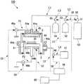
图1是示出用于适用本发明的一实施方式即硅氮化膜的制造方法的等离子体CVD装置的结构的一例的图。FIG. 1 is a diagram showing an example of the configuration of a plasma CVD apparatus to which a method for manufacturing a silicon nitride film according to an embodiment of the present invention is applied.
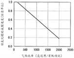
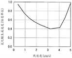
图2是示出气体比率与BHF蚀刻速率的关系的图表。FIG. 2 is a graph showing gas ratio versus BHF etch rate.
图3是示出气体比率与氧化膜生成速度的关系的图表。FIG. 3 is a graph showing the relationship between the gas ratio and the oxide film formation rate.
图4是示出气体比率与硅氮化膜的成膜速度的关系的图表。FIG. 4 is a graph showing the relationship between the gas ratio and the film formation rate of the silicon nitride film.
图5是示出压力与BHF蚀刻速率的关系的图表。FIG. 5 is a graph showing pressure versus BHF etch rate.
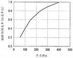
图6是示出压力与氧化膜生成速度的关系的图表。Fig. 6 is a graph showing the relationship between pressure and oxide film formation rate.
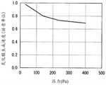
图7是示出线速度与BHF蚀刻速率的关系的图表。FIG. 7 is a graph showing the relationship between linear velocity and BHF etch rate.
图8是示出线速度与氧化膜生成速度的关系的图表。FIG. 8 is a graph showing the relationship between the linear velocity and the oxide film formation rate.
图9是示出高频功率密度与BHF蚀刻速率的关系的图表。FIG. 9 is a graph showing the relationship between high-frequency power density and BHF etching rate.
图10是示出高频功率密度与氧化膜生成速度的关系的图表。FIG. 10 is a graph showing the relationship between high-frequency power density and oxide film formation rate.
具体实施方式Detailed ways
下面,对本发明的一实施方式即硅氮化膜的制造方法,使用附图进行详细说明。此外,下面的说明中使用的附图,为了容易理解特征,方便起见,有时放大示出特征的部分,并不限定各结构要素的尺寸比率等与实际相同。Next, a method for manufacturing a silicon nitride film, which is an embodiment of the present invention, will be described in detail with reference to the drawings. In addition, in the drawings used in the following description, for the sake of easy understanding of features and convenience, features may be shown on an enlarged scale, and the dimensional ratio of each component is not limited to be the same as the actual one.
<硅氮化膜的制造装置><Silicon nitride film production equipment>
首先,对可用于本发明的一实施方式即硅氮化膜的制造方法的、硅氮化膜的制造装置的结构进行说明。即,对用于本实施方式的硅氮化膜的制造方法的、等离子体化学气相沉积装置(等离子体CVD)的结构的一例进行说明。First, the configuration of a silicon nitride film manufacturing apparatus that can be used in a silicon nitride film manufacturing method that is an embodiment of the present invention will be described. That is, an example of the configuration of a plasma chemical vapor deposition apparatus (plasma CVD) used in the method for manufacturing a silicon nitride film according to this embodiment will be described.
图1是示出用于本发明的一实施方式即硅氮化膜的制造方法的等离子体CVD装置的结构的一例的图。如图1所示,等离子体CVD装置100大致构成为具备:基板20、工艺腔室40、工作台41、加热器44a、44b、喷头气体导入部45、电源46a、46b、真空泵47、排气流量调整器48、控制部49、有机硅烷气体供给源50、第一氢还原气体供给源52、第二氢还原气体供给源54、气体流量调整器51、53、55、计算机60和绝缘部S。FIG. 1 is a diagram showing an example of the structure of a plasma CVD apparatus used in a method of manufacturing a silicon nitride film according to an embodiment of the present invention. As shown in FIG. 1 , the
基板20设置在工作台41上,在基板20上制造硅氮化膜30。作为基板的材质,只要具有在成膜温度250℃的耐热性,则并不特别限定,具体而言,例如可以使用石英等。The
工艺腔室40具有基板20、工作台41、加热器44a、44b和喷头气体导入部45。从有机硅烷气体供给源50将有机硅烷气体供给到工艺腔室40内,从第一氢还原气体供给源52和第二氢还原气体供给源54将氢还原气体供给到工艺腔室40内,而制造硅氮化膜30。The
工作台41设置在工艺腔室40的中央附近。The
加热器44a设置在喷头气体导入部45的上部和工艺腔室40的侧面,加热器44b设置在工作台41的下部,能够调整工艺腔室40内和基板20的温度。基板温度的上限并不特别限定,从对低温成膜的要求的背景来看,优选设定为250℃以下。The
喷头气体导入部45设置在工艺腔室40的上部,经由喷头气体导入部45将有机硅烷气体和氢还原气体导入工艺腔室40内。The shower head
电源46a经由电源布线P1与喷头气体导入部45连接。另一方面,电源46b经由电源布线P2与工作台41连接。电源46a通过对喷头气体导入部45施加规定频率的功率,从而能够使从喷头气体导入部45吐出的、混合了有机硅烷气体与氢还原气体的气体等离子化。工作台41根据需要通过电源46b被施加规定频率的功率,将生成的等离子体供给到工作台41上的基板20。在被暴露于该等离子体的基板20上制造硅氮化膜30。作为电源46a、46b并不特别限定,具体而言,例如可以使用高频电源等。另外,还能够同时使用多个电源。The
真空泵47经由排气管路L4与工艺腔室40连接。通过真空泵47,能够进行工艺腔室40内的减压和在硅氮化膜30的制造后生成的气体的排气。The
排气流量调整器48设置在排气管路L4,能够调整通过真空泵47排气的气体的排气流量。作为排气流量调整器48,并不特别限定,可以手动进行控制,还可以通过外部的控制装置自动进行控制。The
控制部49经由信号线C1与加热器44a连接,经由信号线C2与加热器44b连接,经由信号线C3与电源46a连接,经由信号线C4与电源46b连接,经由信号线C5与气体流量调整器51连接,经由信号线C6与气体流量调整器53连接,经由信号线C7与气体流量调整器55连接,经由信号线C8与排气流量调整器48连接。通过控制部49,能够控制加热器44a、44b、电源46a、46b、气体流量调整器51、53、55和排气流量调整器48。控制部49与计算机60连接。The
有机硅烷气体供给源50经由气体供给管路L1,与设置于工艺腔室40的喷头气体导入部45连接,能够将有机硅烷气体供给到工艺腔室40内。作为有机硅烷气体供给源50,并不特别限定,具体而言,例如可以使用填充了有机硅烷气体的瓶等。The organosilane
另外,作为有机硅烷气体,并不特别限定,具体而言,例如可以使用四(二甲氨基)硅烷、三(二甲氨基)硅烷、双(二甲氨基)硅烷、四(二乙氨基)硅烷、三(二乙氨基)硅烷、双(二乙氨基)硅烷、四(乙基甲基氨基)硅烷、三(乙基甲基氨基)硅烷、双(乙基甲基氨基)硅烷等。In addition, the organosilane gas is not particularly limited, and specifically, for example, tetrakis(dimethylamino)silane, tris(dimethylamino)silane, bis(dimethylamino)silane, tetrakis(diethylamino)silane, , Tris(diethylamino)silane, bis(diethylamino)silane, tetrakis(ethylmethylamino)silane, tris(ethylmethylamino)silane, bis(ethylmethylamino)silane, etc.
第一氢还原气体供给源52经由第一氢还原气体供给管路L2和气体供给管路L1,与设置于工艺腔室40的喷头气体导入部45连接,能够将氢还原气体供给到工艺腔室40内。作为第一氢还原气体供给源52,并不特别限定,具体而言,例如可以使用填充了氢还原气体供给源的瓶等。The first hydrogen reducing
另外,作为氢还原气体,并不特别限定,具体而言,可以使用氢气(H2)、氨气(NH3)、胺类、烃类等。In addition, the hydrogen reducing gas is not particularly limited, and specifically, hydrogen (H2 ), ammonia (NH3 ), amines, hydrocarbons, and the like can be used.
第二氢还原气体供给源54经由第二氢还原气体供给管路L3和气体供给管路L1,与设置于工艺腔室40的喷头气体导入部45连接,能够将氢还原气体供给到工艺腔室40内。另外,除了第一氢还原气体供给源52以外,通过使用第二氢还原气体供给源54,从而能够使用混合两种氢还原气体的物质。作为第二氢还原气体供给源54,并不特别限定,具体而言,例如可以使用填充了氢还原气体供给源的瓶等。The second hydrogen reducing
气体流量调整器51设置于气体供给管路L1且与第一氢还原气体供给管路L2的接合部的一次侧,能够调整从有机硅烷气体供给源50供给的有机硅烷气体的流量。另外,气体流量调整器53设置于第一氢还原气体供给管路L2,能够调整从第一氢还原气体供给源52供给的氢还原气体的流量。进而,气体流量调整器55设置于第二氢还原气体供给管路L3,能够调整从第二氢还原气体供给源54供给的氢还原气体的流量。作为气体流量调整器51、53、55,并不特别限定,可以手动进行控制,还可以通过外部的控制装置自动进行控制。The
绝缘部S设置在喷头气体导入部45与工艺腔室40之间,能够电绝缘喷头气体导入部45与工艺腔室40。另外,绝缘部S也设置在工作台41与工艺腔室40之间,能够电绝缘工作台41与工艺腔室40。The insulation part S is disposed between the showerhead
<硅氮化膜的制造方法><Manufacturing method of silicon nitride film>
接着,对使用上述的等离子体CVD装置100的、本实施方式的硅氮化膜的制造方法(以下,仅称为“制造方法”)进行说明。Next, a method of manufacturing a silicon nitride film according to the present embodiment (hereinafter, simply referred to as "manufacturing method") using the above-described
本实施方式的制造方法为通过等离子体化学气相沉积法(等离子体CVD法)制造具有所需的膜特性的硅氮化膜的方法,包括:以规定的气体导入条件将处理气体导入工艺腔室40内的工序;通过施加高频功率对处理气体进行等离子体激发的工序;以及使用等离子体活性物质在基板20上制造硅氮化膜30的工序。更具体而言,在上述的等离子体CVD法中,其特征在于,将有机硅烷气体作为原料气体,将成膜温度设为250℃以下,并且使用对于1体积流量的有机硅烷气体添加了200~2000体积流量的氢还原气体的处理气体,将工艺腔室40内的压力调整为35~400Pa的范围内,将对设置于工艺腔室40内的喷头气体导入部45施加的高频的功率密度调整为0.2~3.5W/cm2的范围内。此外,关于膜特性评价方法将在后面叙述。The manufacturing method of this embodiment is a method of manufacturing a silicon nitride film having desired film properties by plasma chemical vapor deposition (plasma CVD method), including: introducing a processing gas into a process chamber under prescribed gas introduction conditions The process in 40; the process of plasma exciting the process gas by applying high-frequency power; and the process of manufacturing the
下面,对本实施方式的制造方法进行详细说明。Next, the manufacturing method of this embodiment will be described in detail.
首先,将基板20设置于工作台41,通过加热器44b进行加热,直到基板20达到规定的温度。基板温度的上限并不特别限定,从对低温成膜的要求的背景来看,优选设定为250℃以下。First, the
接着,将从有机硅烷气体供给源50供给的有机硅烷气体使用从第一氢还原气体供给源52和第二氢还原气体供给源54供给的大量的氢还原气体稀释之后,经由气体供给管路L1,供给到工艺腔室40内。此外,通过进行上述的稀释操作,在削减碳原子和氢原子对膜的进入量的效果的基础上,还可得到在膜中不形成键合能低的C=C键的效果。Next, after diluting the organosilane gas supplied from the organosilane
这里,关于氢还原气体相对于1体积流量的有机硅烷气体的气体比率和膜特性的关系,图2~图4分别示出本申请发明人们研究的结果。Here, FIG. 2 to FIG. 4 each show the results of studies by the inventors of the present application regarding the relationship between the gas ratio of the hydrogen reducing gas to the organic silane gas at 1 volume flow rate and the film properties.
图2是示出气体比率与BHF蚀刻速率的关系的图表。图2中,横轴表示氢还原气体相对于1体积流量的有机硅烷气体的气体比率。另一方面,纵轴表示BHF蚀刻速率,值越小表示耐氢氟酸性越高。FIG. 2 is a graph showing gas ratio versus BHF etch rate. In FIG. 2 , the horizontal axis represents the gas ratio of the hydrogen reducing gas to the organosilane gas at 1 volume flow rate. On the other hand, the vertical axis represents the BHF etching rate, and the smaller the value, the higher the hydrofluoric acid resistance.
根据图2可知,在本实施方式的制造方法中具有增加上述气体比率时耐氢氟酸性提高的倾向。另一方面,可知具有减少上述气体比率时耐氢氟酸性降低的倾向。As can be seen from FIG. 2 , in the production method of the present embodiment, the hydrofluoric acid resistance tends to improve as the gas ratio is increased. On the other hand, it can be seen that the resistance to hydrofluoric acid tends to decrease when the gas ratio is reduced.
图3是示出气体比率与氧化膜生成速度的关系的图表。图3中,横轴表示氢还原气体相对于1体积流量的有机硅烷气体的气体比率。另一方面,纵轴表示氧化膜生成速度,值越小表示耐湿性越高。此外,在本申请发明的硅氮化膜中,氧化膜的生成从硅氮化膜的表面侧进行,另行通过实验确认水分并不会向生成的氧化膜的膜厚以上更深的地方透过。根据图3可知,在本实施方式的制造方法中具有增加上述气体比率时耐湿性提高的倾向。另一方面,可知具有减少上述气体比率时耐湿性降低的倾向。FIG. 3 is a graph showing the relationship between the gas ratio and the oxide film formation rate. In FIG. 3 , the horizontal axis represents the gas ratio of the hydrogen reducing gas to the organic silane gas at 1 volume flow rate. On the other hand, the vertical axis represents the oxide film formation rate, and the smaller the value, the higher the moisture resistance. In addition, in the silicon nitride film of the present invention, the formation of the oxide film progresses from the surface side of the silicon nitride film, and it has been confirmed through experiments that moisture does not permeate deeper than the film thickness of the formed oxide film. As can be seen from FIG. 3 , in the production method of the present embodiment, the moisture resistance tends to improve when the gas ratio is increased. On the other hand, it turns out that there exists a tendency for moisture resistance to fall when the said gas ratio is reduced.
图4是示出气体比率与硅氮化膜的成膜速度的关系的图表。图4中,横轴表示氢还原气体相对于1体积流量的有机硅烷气体的气体比率。另一方面,纵轴表示硅氮化膜的成膜速度,值越大表示硅氮化膜的成膜速度越快。根据图4可知,在本实施方式的制造方法中具有增加上述气体比率时硅氮化膜的成膜速度降低的倾向。另一方面,可知具有气体比率减少时硅氮化膜的成膜速度增加的倾向。FIG. 4 is a graph showing the relationship between the gas ratio and the film formation rate of the silicon nitride film. In FIG. 4 , the horizontal axis represents the gas ratio of the hydrogen reducing gas to the organosilane gas at 1 volume flow rate. On the other hand, the vertical axis represents the film formation rate of the silicon nitride film, and the larger the value, the faster the film formation rate of the silicon nitride film. As can be seen from FIG. 4 , in the manufacturing method of the present embodiment, the film formation rate of the silicon nitride film tends to decrease when the gas ratio is increased. On the other hand, it can be seen that the film formation rate of the silicon nitride film tends to increase as the gas ratio decreases.
根据上述研究结果可知越是提高氢还原气体相对于1体积流量的有机硅烷气体的气体比率,耐氢氟酸性和耐湿性越提高,但另一方面成膜速度降低,生产率降低。因此,在本实施方式的制造方法中,优选使用对于1体积流量的有机硅烷气体添加了200~2000体积流量的氢还原气体的处理气体。From the above research results, it can be seen that the higher the gas ratio of the hydrogen reducing gas to the organosilane gas at 1 volume flow rate, the higher the hydrofluoric acid resistance and the humidity resistance, but on the other hand, the film formation rate decreases and the productivity decreases. Therefore, in the manufacturing method of this embodiment, it is preferable to use the processing gas which added 200-2000 volume flow rate of hydrogen reducing gas with respect to 1 volume flow rate of organosilane gas.
此外,上述气体比率的调整通过调整各气体的流量进行。具体而言,通过气体流量调整器51调整有机硅烷气体的流量,通过气体流量调整器53调整从第一氢还原气体供给源52供给的氢还原气体的流量,通过气体流量调整器55调整从第二氢还原气体供给源54供给的氢还原气体的流量来进行调整。In addition, the adjustment of the said gas ratio is performed by adjusting the flow rate of each gas. Specifically, the flow rate of the organosilane gas is adjusted by the
另一方面,在上述处理气体被供给的工艺腔室40中,通过真空泵47控制内部的压力。工艺腔室40内的压力会影响原料气体在等离子体中开始分解到在基板20上进行反应为止的工艺腔室40内的滞留时间、等离子体放电状态以及碰撞频度,其结果是也会对制造的硅氮化膜的膜特性造成影响。具体而言,降低压力时碰撞频度下降导致解离变得不充分,进一步降低时等离子体状态不稳定变得不充分。另一方面,提高压力时平均自由行程缩短导致无法得到充分的加速能,进一步提高时等离子体状态的维持变得困难。On the other hand, in the
这里,对于工艺腔室40内的压力与膜特性的关系,图5和图6中分别示出本申请发明人们研究的结果。Here, with regard to the relationship between the pressure in the
图5是示出压力与BHF蚀刻速率的关系的图表。图5中,横轴表示工艺腔室40内的压力。另一方面,纵轴表示BHF蚀刻速率,值越小表示耐氢氟酸性越高。根据图5可知,在本实施方式的制造方法中具有增加工艺腔室40内的压力时耐氢氟酸性降低的倾向。另一方面,可知具有减少工艺腔室40内的压力时耐氢氟酸性提高的倾向。FIG. 5 is a graph showing pressure versus BHF etch rate. In FIG. 5 , the horizontal axis represents the pressure in the
图6是示出压力与氧化膜生成速度的关系的图表。图6中,横轴表示工艺腔室40内的压力。另一方面,纵轴表示氧化膜生成速度,值越小表示耐湿性越高。根据图6可知,在本实施方式的制造方法中具有增加工艺腔室40内的压力时耐湿性降低的倾向。另一方面,可知具有减少工艺腔室40内的压力时耐湿性降低的倾向。Fig. 6 is a graph showing the relationship between pressure and oxide film formation rate. In FIG. 6 , the horizontal axis represents the pressure in the
根据上述研究结果可知越是提高工艺腔室40内的压力,则耐湿性提高,另一方面耐氢氟酸性降低。因此,在本实施方式的制造方法中,优选将工艺腔室40内的压力调整为35~400Pa的范围。From the above research results, it can be seen that the higher the pressure in the
另外,通过气体流量调整器51、53、55和压力控制供给到工艺腔室40内的处理气体的线速度。与工艺腔室40内的压力同样,处理气体的线速度也会影响原料气体在等离子体中开始分解到在基板20上进行反应位置的工艺腔室内的滞留时间、等离子体放电状态以及碰撞频度。In addition, the linear velocity of the processing gas supplied into the
这里,对于处理气体的线速度与膜特性的关系,图7和图8中分别示出本申请发明人们研究的结果。Here, FIG. 7 and FIG. 8 respectively show the results of studies by the inventors of the present application regarding the relationship between the linear velocity of the processing gas and the film properties.
图7是示出线速度与BHF蚀刻速率的关系的图表。图7中,横轴表示处理气体的线速度。另一方面,纵轴表示BHF蚀刻速率,值越小表示耐氢氟酸性越高。根据图7可知,在本实施方式的制造方法中,线速度在1.0cm/秒附近BHF蚀刻速率取极小值,耐氢氟酸性变得最佳。FIG. 7 is a graph showing the relationship between linear velocity and BHF etch rate. In FIG. 7 , the horizontal axis represents the linear velocity of the processing gas. On the other hand, the vertical axis represents the BHF etching rate, and the smaller the value, the higher the hydrofluoric acid resistance. As can be seen from FIG. 7 , in the manufacturing method of this embodiment, the BHF etching rate takes a minimum value at a linear velocity around 1.0 cm/sec, and the hydrofluoric acid resistance becomes optimal.
图8是示出线速度与氧化膜生成速度的关系的图表。图8中,横轴表示处理气体的线速度。另一方面,纵轴表示氧化膜生成速度,值越小表示耐湿性越高。根据图8可知,在本实施方式的制造方法中,线速度在3.0cm/秒附近耐湿性指标取极小值,耐湿性变得最佳。FIG. 8 is a graph showing the relationship between the linear velocity and the oxide film formation rate. In FIG. 8 , the horizontal axis represents the linear velocity of the process gas. On the other hand, the vertical axis represents the oxide film formation rate, and the smaller the value, the higher the moisture resistance. As can be seen from FIG. 8 , in the manufacturing method of this embodiment, the moisture resistance index takes a minimum value at a linear velocity around 3.0 cm/sec, and the moisture resistance becomes optimal.
根据上述研究结果可知,关于线速度,过快或过慢,都会降低生成适度的解离状态的活性物质的效率,无法得到优质的膜。因此,在本实施方式的制造方法中,优选处理气体的线速度调整为0.3~5.0cm/秒的范围。From the above research results, it can be seen that too high or too low a linear velocity reduces the efficiency of producing an active material in a moderately dissociated state, and a high-quality film cannot be obtained. Therefore, in the manufacturing method of the present embodiment, it is preferable to adjust the linear velocity of the processing gas to a range of 0.3 to 5.0 cm/sec.
接着,对喷头气体导入部45通过电源46a施加规定频率的功率,激发从气体供给管路L1供给的、含有有机硅烷气体和氢还原气体的处理气体,形成等离子体。Next, power of a predetermined frequency is applied to the shower head
此外,在本实施方式的制造方法中,施加功率的频率并不特别限定,可以从60MHz以下的频率中适当选定。作为一例,通过连续或间歇地使用380kHz和13.56MHz的某一方或同时使用双方,从而能够起到本实施方式的至少一部分效果。施加的功率会影响有机硅烷气体和氢还原气体的解离状态。In addition, in the manufacturing method of the present embodiment, the frequency of the applied power is not particularly limited, and can be appropriately selected from frequencies of 60 MHz or less. As an example, at least part of the effects of this embodiment can be exhibited by continuously or intermittently using one of 380 kHz and 13.56 MHz, or using both of them simultaneously. The applied power affects the dissociation states of organosilane gas and hydrogen reducing gas.
这里,对于高频功率密度与膜特性的关系,图9和图10中分别示出本申请发明人们研究的结果。Here, with regard to the relationship between the high-frequency power density and the film properties, FIG. 9 and FIG. 10 respectively show the results of studies by the inventors of the present application.
图9是示出高频功率密度与BHF蚀刻速率的关系的图表。图9中,横轴表示高频功率密度。另一方面,纵轴表示BHF蚀刻速率,值越小表示耐氢氟酸性越高。根据图9可知,在本实施方式的制造方法中具有增加高频功率密度时耐氢氟酸性提高的倾向。另一方面,可知具有减少高频功率密度时,耐氢氟酸性降低的倾向。FIG. 9 is a graph showing the relationship between high-frequency power density and BHF etching rate. In FIG. 9 , the horizontal axis represents the high-frequency power density. On the other hand, the vertical axis represents the BHF etching rate, and the smaller the value, the higher the hydrofluoric acid resistance. As can be seen from FIG. 9 , in the production method of the present embodiment, the hydrofluoric acid resistance tends to improve when the high-frequency power density is increased. On the other hand, it can be seen that when the high-frequency power density is reduced, the resistance to hydrofluoric acid tends to decrease.
图10是示出高频功率密度与耐湿性指标的关系的图表。图10中,横轴表示功率密度。另一方面,纵轴表示氧化膜生成速度,值越小表示耐湿性越高。根据图10可知,在本实施方式的制造方法中具有增加高频功率密度时耐湿性提高的倾向。另一方面,可知具有减少高频功率密度时耐湿性降低的倾向。FIG. 10 is a graph showing the relationship between the high-frequency power density and the moisture resistance index. In FIG. 10 , the horizontal axis represents power density. On the other hand, the vertical axis represents the oxide film formation rate, and the smaller the value, the higher the moisture resistance. As can be seen from FIG. 10 , in the manufacturing method of the present embodiment, the moisture resistance tends to improve when the high-frequency power density is increased. On the other hand, it can be seen that the moisture resistance tends to decrease when the high-frequency power density is decreased.
根据上述研究结果可知越是增加高频功率密度,耐氢氟酸性和耐湿性越是提高。但是,另一方面,为了回避高频电源初始投资、功耗成本和等离子体发生装置部件的耐久性等问题,高频功率密度优选为3.0W/cm2以下。From the above research results, it can be seen that the higher the high-frequency power density is, the more the hydrofluoric acid resistance and the moisture resistance are improved. However, on the other hand, in order to avoid problems such as initial investment in high-frequency power supply, power consumption cost, and durability of plasma generator components, the high-frequency power density is preferably 3.0 W/cm2 or less.
另外,高频功率密度为0.4W/cm2以上时,原料的分解加速,成膜速度变为1nm/min以上,从生产率方面来看优选。In addition, when the high-frequency power density is 0.4 W/cm2 or more, the decomposition of the raw material is accelerated, and the film formation rate becomes 1 nm/min or more, which is preferable from the viewpoint of productivity.
0.2W/cm2以下时,原料难以分解,SiN难以形成,因此从生产率方面来看不优选。When it is 0.2 W/cm2 or less, the raw material is difficult to decompose and SiN is difficult to form, so it is not preferable from the viewpoint of productivity.
还可知由于硅氮化膜的成膜速度下降,因此没有生产率,3.5W/cm2时,根据设备会对基板造成损坏而设备性能恶化。It can also be seen that the productivity of the silicon nitride film is lowered due to a decrease in the film formation rate, and that at 3.5 W/cm2 , the substrate is damaged depending on the equipment and the performance of the equipment is deteriorated.
因此,考虑上述效果和问题,在本发明的硅氮化膜的制造方法中,高频功率密度优选调整为0.4~3.0W/cm2的范围。Therefore, in consideration of the above-mentioned effects and problems, in the method for producing a silicon nitride film of the present invention, the high-frequency power density is preferably adjusted to a range of 0.4 to 3.0 W/cm2 .
此外,上述高频功率密度为进行高频施加的电极面积为452cm2时的数值,设为0.2W/cm2以上时,高频功率为90W以上即可,设为3.5W/cm2以下时,高频功率为1583W以下即可。In addition, the above-mentioned high-frequency power density is a value when the electrode area for high-frequency application is 452 cm2 , and when it is set to 0.2 W/cm2 or more, the high-frequency power can be 90 W or more, and when it is set to 3.5 W/cm2 or less , The high-frequency power is below 1583W.
最后,通过将形成的等离子体供给到基板20,从而在基板20上制造硅氮化膜30。此外,在硅氮化膜30的制造后产生气体,通过真空泵47,经由排气管路L4,将产生的气体向工艺腔室40的外部排气。这样,能够制造具有以下所示的膜特性的硅氮化膜。Finally, by supplying the formed plasma to the
<硅氮化膜><Silicon nitride film>
通过上述的本实施方式的制造方法得到的硅氮化膜,即使用等离子体CVD装置100,将有机硅烷气体作为原料气体,将成膜温度设为250℃以下,使用对于1体积流量的有机硅烷气体添加了200~2000体积流量的氢还原气体的处理气体,将工艺腔室40内的压力调整为35~400Pa的范围内,将对设置于工艺腔室40内的电极施加的高频的功率密度调整为0.2~3.5W/cm2的范围内来成膜的硅氮化膜,具有下述(a)~(c)所示的膜特性:The silicon nitride film obtained by the production method of the present embodiment described above uses the
(a)利用氢氟酸溶液的被蚀刻速率为10nm/min以下;(a) The etching rate by hydrofluoric acid solution is below 10nm/min;
(b)在暴露于208kPa、121℃的饱和水蒸气气氛的期间内产生的硅氧化物的生成速度以硅氧化膜换算为2nm/hr以下;(b) The formation rate of silicon oxide generated during exposure to a saturated water vapor atmosphere at 208 kPa and 121° C. is 2 nm/hr or less in terms of silicon oxide film;
(c)膜中的内部应力在-1000~1000MPa的范围内。(c) The internal stress in the film is in the range of -1000 to 1000 MPa.
如以上说明所示,根据本实施方式的制造方法,将有机硅烷气体作为原料气体,在成膜温度250℃以下,通过等离子体化学气相沉积法制造硅氮化膜时,使用对于1体积流量的有机硅烷气体添加了200~2000体积流量的氢还原气体的处理气体,将收容基板的工艺腔室40内的压力调整为35~400Pa的范围内,将对设置于工艺腔室40内的电极施加的高频的功率密度调整为0.2~3.5W/cm2的范围内。据此,能够制造具有高的耐氢氟酸性、高耐湿性以及与设备侧的要求相应的适当的内部应力(即,上述(a)~(c)的膜特性)的硅氮化膜。As described above, according to the production method of this embodiment, when a silicon nitride film is produced by plasma chemical vapor deposition at a film formation temperature of 250° C. The organic silane gas is added with 200-2000 volume flow rate of hydrogen reducing gas processing gas, the pressure in the
此外,根据本实施方式的制造方法,优选将导入工艺腔室内的所述处理气体的线速度调整为0.3~5.0cm/秒的范围。In addition, according to the manufacturing method of this embodiment, it is preferable to adjust the linear velocity of the processing gas introduced into the process chamber to be in the range of 0.3 to 5.0 cm/sec.
在下述PCT结果中,硅氮化膜的生成速度2nm/hr与一般性的透湿度评价方法的0.2g/m2/day同等。In the following PCT results, the silicon nitride film formation rate of 2 nm/hr is equivalent to 0.2 g/m2 /day in a general moisture permeability evaluation method.
此外,本发明的技术范围并不限定于上述实施方式,在不脱离本发明的宗旨的范围内可以施加各种变更。例如,在上述的实施方式的制造方法中,对通过使用第一氢还原气体供给源52和第二氢还原气体供给源54来使用两种氢还原气体的例子进行了说明,但氢还原气体供给源也可以为一个。In addition, the technical scope of this invention is not limited to the said embodiment, Various changes can be added in the range which does not deviate from the summary of this invention. For example, in the manufacturing method of the above-mentioned embodiment, an example in which two kinds of hydrogen reducing gases are used by using the first hydrogen reducing
实施例Example
<硅氮化膜的制造><Manufacture of Silicon Nitride Film>
作为实施例1~8,根据本发明的硅氮化膜的制造方法,在控制到250℃以下的硅氮化基板上制造硅氮化膜。As Examples 1 to 8, according to the method for producing a silicon nitride film of the present invention, a silicon nitride film was produced on a silicon nitride substrate controlled to be below 250°C.
作为有机硅烷气体使用三(二甲氨基)硅烷(3DMAS)或四(二甲氨基)硅烷(4DMAS),作为氢还原气体使用氢气(H2)。Tris(dimethylamino)silane (3DMAS) or tetrakis(dimethylamino)silane (4DMAS) was used as the organosilane gas, and hydrogen (H2 ) was used as the hydrogen reducing gas.
施加的功率的频率为380kHz或13.56MHz。The frequency of the applied power was 380 kHz or 13.56 MHz.
下述的表1示出各实施例中的、氢还原气体的流量相对于有机硅烷气体的流量的比率、线速度、工艺腔室内的压力、功率密度等制造条件。Table 1 below shows production conditions such as the ratio of the flow rate of the hydrogen reducing gas to the flow rate of the organosilane gas, the line speed, the pressure in the process chamber, and the power density in each example.
作为比较例1、2,使用硅烷气体,在控制到200℃或250℃的硅基板上,以从膜特性的观点来看为最佳的条件,制造硅氮化膜。As Comparative Examples 1 and 2, a silicon nitride film was produced on a silicon substrate controlled at 200° C. or 250° C. under optimum conditions from the viewpoint of film properties using silane gas.
下述的表1中示出比较例1、2的制造条件。The production conditions of Comparative Examples 1 and 2 are shown in Table 1 below.
作为比较例3,使用硅烷气体,在控制到350℃的硅基板上制造硅氮化膜。As Comparative Example 3, a silicon nitride film was produced on a silicon substrate controlled at 350° C. using silane gas.
下述的表1示出比较例3的制造条件。Table 1 below shows the production conditions of Comparative Example 3.
作为比较例4和5,作为有机硅烷气体使用三(二甲氨基)硅烷(3DMAS),作为氢还原气体使用氢气(H2),在控制到200℃的硅基板上制造硅氮化膜。In Comparative Examples 4 and 5, using tris(dimethylamino)silane (3DMAS) as the organosilane gas and hydrogen (H2 ) as the hydrogen reducing gas, a silicon nitride film was produced on a silicon substrate controlled at 200°C.
[表1][Table 1]

<膜特性评价方法><Evaluation method of membrane properties>
对于通过上述的条件制造的硅氮化膜,进行膜特性评价。以下对各评价方法进行说明。Film characteristic evaluation was performed on the silicon nitride film produced under the above-mentioned conditions. Each evaluation method will be described below.
(膜组成)(film composition)
硅氮化膜的原子间键合状态使用FTIR(傅里叶变换红外光谱仪、Perkinelmer制spectrum400)测定红外吸收光谱来评价。具体而言,收集Si-N键、Si-H键、N-H键、C=N键、C=C键和Si-O键等信息并进行分析。The interatomic bonding state of the silicon nitride film was evaluated by measuring an infrared absorption spectrum using FTIR (Fourier Transform Infrared Spectrometer,
(耐湿性)(moisture resistance)
关于硅氮化膜的耐湿性,通过FT-IR收集压力锅试验(PCT:Pressure CookerTest)前后的膜中Si-O键的信息来评价。这里得到的直接的结果为膜的吸湿量。其中,已另行评价了当吸湿量相当于SiO2膜厚1nm时,通过具有换算为SiO2膜为1nm膜厚的硅氮化膜可防止水分透过,因此意味着吸湿量越少的膜水分屏蔽性越高。The moisture resistance of the silicon nitride film was evaluated by collecting information on Si—O bonds in the film before and after a pressure cooker test (PCT: Pressure Cooker Test) by FT-IR. The immediate result obtained here is the moisture uptake of the film. Among them, it has been separately evaluated that moisture permeation can be prevented by having a silicon nitride film having a film thickness of 1 nm in terms of SiO2 when the moisture absorption is equivalent to a SiO2 film thickness of 1 nm, so it means that the film moisture with less moisture absorption The higher the shielding.
此外,PCT的条件设为208kPa、121℃。这相当于常温常压气氛的10000倍的加速试验。In addition, the conditions of PCT were 208 kPa and 121 degreeC. This is equivalent to an accelerated test 10,000 times that of the normal temperature and pressure atmosphere.
(耐氢氟酸性)(hydrofluoric acid resistance)
关于硅氮化膜的耐氢氟酸性,使用BHF(缓冲氢氟酸)溶液进行评价。具体而言,将硅氮化膜浸渍到16BHF(含20.8%NH4HF2水溶液,森田化学工业制),经过规定时间后,迅速用纯水充分清洗,吹氮气等使其干燥,使用下述式(1)评价BHF蚀刻速率R。此外,下述式(1)中的、d1表示浸渍处理前的膜厚,d2表示浸渍处理后的膜厚,t表示浸渍时间,膜厚通过后述的椭圆偏振光谱仪测量。The hydrofluoric acid resistance of the silicon nitride film was evaluated using a BHF (buffered hydrofluoric acid) solution. Specifically, the silicon nitride film was dipped in 16BHF (aqueous solution containing 20.8% NH4 HF2 , manufactured by Morita Chemical Industry Co., Ltd.), and after a predetermined time, it was quickly and sufficiently washed with pure water, and dried by blowing nitrogen gas, etc., using the following Equation (1) evaluates the BHF etch rate R. In addition, in the following formula (1 ), d1 represents the film thickness before the immersion treatment,d2 represents the film thickness after the immersion treatment, and t represents the immersion time, and the film thickness is measured by a spectroscopic ellipsometer described later.
R=(d1-d2)÷t……(1)R=(d1 -d2 )÷t...(1)
(膜的内部应力)(internal stress of membrane)
硅氮化膜的内部应力通过膜应力测定装置(东朋科技制FLX-2320-R)进行测定,该测定装置将根据基板的翘曲的变化量导出作为其测定原理。The internal stress of the silicon nitride film was measured with a film stress measuring device (FLX-2320-R manufactured by Toho Technology Co., Ltd.), which derives the amount of change due to the warpage of the substrate as its measurement principle.
(绝缘性)(insulation)
硅氮化膜的绝缘性通过进行水银探头式的IV测定装置(Solid StateMeasurement制FLX-2320-R)来评价。具体而言,通过电场强度为1MV/cm时的泄漏电流值进行评价。The insulation properties of the silicon nitride film were evaluated with a mercury probe type IV measuring device (FLX-2320-R manufactured by Solid State Measurement). Specifically, the evaluation was performed by the leakage current value when the electric field intensity was 1 MV/cm.
(折射率和膜厚)(refractive index and film thickness)
硅氮化膜的折射率和膜厚使用椭圆偏振光谱仪(SOPRA制GES5E)来测定。The refractive index and film thickness of the silicon nitride film were measured using a spectroscopic ellipsometer (GES5E manufactured by SOPRA).
<膜特性评价结果><Evaluation results of film characteristics>
下述表2示出实施例1~8和比较例1~5的膜特性的评价结果。可知实施例1~8的氢氟酸溶液的蚀刻速率均为10nm/min以下,具有比比较例3高的耐氢氟酸性。另外,如比较例1、2所示,可知硅烷气体无法得到充分的耐氢氟酸性。Table 2 below shows the evaluation results of the film properties of Examples 1-8 and Comparative Examples 1-5. It can be seen that the etching rates of the hydrofluoric acid solutions of Examples 1 to 8 are all 10 nm/min or less, and have higher hydrofluoric acid resistance than Comparative Example 3. In addition, as shown in Comparative Examples 1 and 2, it was found that sufficient hydrofluoric acid resistance cannot be obtained for silane gas.
同样地,可知在暴露于208kPa、121℃的饱和水蒸气气氛的期间内产生的硅氧化物的生成速度以硅氧化膜换算为2nm/hr,实施例1~8具有与比较例1~3相比同等以上的高耐湿性、水分屏蔽性。Similarly, it can be seen that the formation rate of silicon oxide produced during the period of exposure to a saturated water vapor atmosphere at 208 kPa and 121° C. is 2 nm/hr in terms of silicon oxide film, and Examples 1 to 8 have the same characteristics as Comparative Examples 1 to 3. High moisture resistance and moisture barrier performance than the equivalent.
进而,如实施例1和4所示,可知能够制造兼具内部应力非常小的特性的硅氮化膜。另外,可知实施例1~8的内部应力分别示出从﹣562MPa~﹢728MPa范围内的有较大不同的值,能够将具有高的耐氢氟酸性和高的耐湿性的硅氮化膜调整为规定的内部应力来制造。Furthermore, as shown in Examples 1 and 4, it can be seen that a silicon nitride film having a characteristic of very small internal stress can be produced. In addition, it can be seen that the internal stresses of Examples 1 to 8 show values that vary greatly from -562MPa to +728MPa, respectively, and it is possible to adjust the silicon nitride film having high hydrofluoric acid resistance and high moisture resistance. Manufactured for specified internal stress.
进而,除了实施例7,施加1MV/cm的电场时的泄漏电流值为1.0×10-6A/cm2以下,可知兼具高绝缘性。特别是关于实施例1,可知虽然不及将硅烷气体作为原料气体的比较例,但是具有7×10-8A/cm2以下的优异的绝缘性。Furthermore, except for Example 7, the leakage current value when an electric field of 1 MV/cm was applied was 1.0×10⁻⁶ A/cm2 or less, and it was found that both high insulation properties were achieved. In particular, Example 1 was found to have an excellent insulating property of 7×10⁻⁸ A/cm2 or less, although it was not as good as the comparative example using silane gas as a source gas.
另一方面,可知在比较例4中,将硅氮化膜的制造条件中的有机硅烷气体和氢还原气体的流量比设为133时,在暴露于208kPa、121℃的饱和水蒸气气氛的期间内产生的硅氧化物的生成速度以硅氧化膜换算为2.3nm/hr,耐湿性、水分屏蔽性下降。On the other hand, in Comparative Example 4, when the flow rate ratio of the organosilane gas and the hydrogen reducing gas in the production conditions of the silicon nitride film was set to 133, the The generation rate of the silicon oxide formed in the silicon oxide film was 2.3nm/hr in terms of silicon oxide film, and the moisture resistance and the moisture barrier property were lowered.
另外,可知在比较例5中,将硅氮化膜的制造条件中的线速度设为0.2cm/秒时,在暴露于208kPa、121℃的饱和水蒸气气氛的期间内产生的硅氧化物的生成速度以硅氧化膜换算为29.2nm/hr,耐湿性、水分屏蔽性下降。In addition, in Comparative Example 5, when the linear velocity in the production conditions of the silicon nitride film was set to 0.2 cm/sec, it was found that the amount of silicon oxide produced during the period of exposure to a saturated water vapor atmosphere at 208 kPa and 121° C. The formation rate was 29.2nm/hr in terms of silicon oxide film, and the moisture resistance and moisture barrier properties were lowered.
[表2][Table 2]

本发明的硅氮化膜的制造方法和硅氮化膜可利用于电子设备或光学设备等半导体装置的制造工序中的掩膜材料、构成半导体装置的防金属扩散膜、氧化屏蔽膜、钝化膜、绝缘膜等及其制造方法。The method for producing a silicon nitride film and the silicon nitride film of the present invention can be used as a mask material in the manufacturing process of semiconductor devices such as electronic equipment or optical equipment, as a metal diffusion prevention film constituting a semiconductor device, an oxidation mask film, a passivation film, etc. Films, insulating films, etc., and production methods thereof.
附图标记说明Explanation of reference signs
20 基板20 substrates
30 硅氮化膜30 silicon nitride film
40 工艺腔室40 process chambers
41 工作台41 Workbench
44a、44b 加热器44a, 44b heater
45 喷头气体导入部45 Nozzle gas introduction part
46a、46b 电源46a, 46b power supply
47 真空泵47 vacuum pump
48 排气流量调整器48 Exhaust flow regulator
49 控制部49 Control Department
50 有机硅烷气体供给源50 organosilane gas supply source
51 气体流量调整器51 Gas flow regulator
52 第一氢还原气体供给源52 The first hydrogen reducing gas supply source
53 气体流量调整器53 Gas flow regulator
54 第二氢还原气体供给源54 Second hydrogen reducing gas supply source
55 气体流量调整器55 Gas flow regulator
60 计算机60 computers
100 等离子体CVD装置100 Plasma CVD device
S 绝缘部S Insulation
L1 气体供给管路L1 Gas supply line
L2 第一氢还原气体供给管路L2 first hydrogen reducing gas supply pipeline
L3 第二氢还原气体供给管路L3 Second hydrogen reducing gas supply pipeline
L4 排气管路L4 exhaust line
C1、C2、C3、C4、C5、C6、C7、C8 信号线C1, C2, C3, C4, C5, C6, C7, C8 signal lines
P1、P2 电源布线P1, P2 power wiring
Claims (4)
Applications Claiming Priority (1)
| Application Number | Priority Date | Filing Date | Title |
|---|---|---|---|
| PCT/JP2016/057781WO2017154202A1 (en) | 2016-03-11 | 2016-03-11 | Method for producing silicon nitride film, and silicon nitride film |
Publications (2)
| Publication Number | Publication Date |
|---|---|
| CN108713243A CN108713243A (en) | 2018-10-26 |
| CN108713243Btrue CN108713243B (en) | 2022-11-01 |
Family
ID=59789279
Family Applications (1)
| Application Number | Title | Priority Date | Filing Date |
|---|---|---|---|
| CN201680083268.3AActiveCN108713243B (en) | 2016-03-11 | 2016-03-11 | Method for producing silicon nitride film and silicon nitride film |
Country Status (5)
| Country | Link |
|---|---|
| US (1) | US10559459B2 (en) |
| EP (1) | EP3428959B1 (en) |
| KR (1) | KR102418092B1 (en) |
| CN (1) | CN108713243B (en) |
| WO (1) | WO2017154202A1 (en) |
Families Citing this family (2)
| Publication number | Priority date | Publication date | Assignee | Title |
|---|---|---|---|---|
| JP7572168B2 (en)* | 2020-05-29 | 2024-10-23 | 大陽日酸株式会社 | Mixed gas supply device, metal nitride film manufacturing device, and metal nitride film manufacturing method |
| CN114709295B (en)* | 2022-06-06 | 2022-09-02 | 一道新能源科技(衢州)有限公司 | A method and device for reducing attenuation of perc cell |
Citations (6)
| Publication number | Priority date | Publication date | Assignee | Title |
|---|---|---|---|---|
| JPH0917778A (en)* | 1995-07-03 | 1997-01-17 | Fujitsu Ltd | High frequency plasma CVD equipment |
| US5629043A (en)* | 1994-12-15 | 1997-05-13 | Mitsubishi Denki Kabushiki Kaisha | Silicon nitride film formation method |
| JP2004292877A (en)* | 2003-03-26 | 2004-10-21 | Ishikawa Seisakusho Ltd | Silicon nitride film and method for manufacturing the same |
| CN101454880A (en)* | 2006-05-31 | 2009-06-10 | 东京毅力科创株式会社 | Plasma cvd method, method for forming silicon nitride film, method for manufacturing semiconductor device and plasma cvd method |
| JP2010192479A (en)* | 2009-02-14 | 2010-09-02 | Philtech Inc | Metal substrate, device for forming thin film on metal substrate and solar cell using metal substrate |
| JP2013122068A (en)* | 2011-12-09 | 2013-06-20 | Ulvac Japan Ltd | Method for forming tungsten compound film and semiconductor device |
Family Cites Families (26)
| Publication number | Priority date | Publication date | Assignee | Title |
|---|---|---|---|---|
| JPS5269093A (en) | 1975-12-06 | 1977-06-08 | Tohatsu Kk | Jig for arranging plates in order for use in device for cutting plateeshaped goods |
| JPH06132284A (en) | 1992-10-22 | 1994-05-13 | Kawasaki Steel Corp | Method for forming protective film of semiconductor device |
| JP2641385B2 (en)* | 1993-09-24 | 1997-08-13 | アプライド マテリアルズ インコーポレイテッド | Film formation method |
| JPH07221026A (en) | 1994-01-28 | 1995-08-18 | Mitsui Toatsu Chem Inc | Method for forming high quality semiconductor thin film |
| TW362118B (en) | 1995-10-30 | 1999-06-21 | Dow Corning | Method for depositing amorphous SiNC coatings |
| DE60127973T2 (en) | 2000-08-18 | 2008-01-17 | Tokyo Electron Ltd. | PRODUCTION PROCESS OF SEMICONDUCTOR COMPONENT WITH SILICON NITRIDE INTERMEDIATE WITH LOW DIELECTRIC CONSTANT |
| EP1592051A4 (en) | 2003-01-24 | 2012-02-22 | Tokyo Electron Ltd | CVD method for forming a silicon nitride film on a target substrate |
| JP4228150B2 (en) | 2005-03-23 | 2009-02-25 | 東京エレクトロン株式会社 | Film forming apparatus, film forming method, and storage medium |
| JP2008270706A (en)* | 2007-03-26 | 2008-11-06 | Tokyo Electron Ltd | Silicon nitride film and nonvolatile semiconductor memory device |
| JP5069531B2 (en)* | 2007-09-28 | 2012-11-07 | 富士フイルム株式会社 | Method for forming silicon nitride film |
| US7678715B2 (en) | 2007-12-21 | 2010-03-16 | Applied Materials, Inc. | Low wet etch rate silicon nitride film |
| JP2010103484A (en) | 2008-09-29 | 2010-05-06 | Adeka Corp | Semiconductor device, apparatus and method for manufacturing the same |
| JP2011023718A (en) | 2009-07-15 | 2011-02-03 | Asm Japan Kk | METHOD FOR FORMING STRESS-TUNED DIELECTRIC FILM HAVING Si-N BOND BY PEALD |
| JP2011089186A (en) | 2009-10-26 | 2011-05-06 | Tosoh Corp | Silicon carbonitride-containing film, method for producing the same, and usage of the same |
| US8709551B2 (en)* | 2010-03-25 | 2014-04-29 | Novellus Systems, Inc. | Smooth silicon-containing films |
| US20130157466A1 (en)* | 2010-03-25 | 2013-06-20 | Keith Fox | Silicon nitride films for semiconductor device applications |
| JP5731841B2 (en) | 2011-02-02 | 2015-06-10 | 大陽日酸株式会社 | Method for forming silicon nitride film |
| JP5941653B2 (en) | 2011-02-24 | 2016-06-29 | 東京エレクトロン株式会社 | Silicon nitride film forming method and silicon nitride film forming apparatus |
| US8771807B2 (en) | 2011-05-24 | 2014-07-08 | Air Products And Chemicals, Inc. | Organoaminosilane precursors and methods for making and using same |
| JP5922352B2 (en)* | 2011-08-11 | 2016-05-24 | Sppテクノロジーズ株式会社 | NITRIDE FILM MANUFACTURING DEVICE, ITS MANUFACTURING METHOD, AND ITS MANUFACTURING PROGRAM |
| US8592328B2 (en) | 2012-01-20 | 2013-11-26 | Novellus Systems, Inc. | Method for depositing a chlorine-free conformal sin film |
| TW201341569A (en) | 2012-02-14 | 2013-10-16 | Novellus Systems Inc | Silicon nitride films for semiconductor device applications |
| JP2014060378A (en) | 2012-08-23 | 2014-04-03 | Tokyo Electron Ltd | Silicon nitride film deposition method, organic electronic device manufacturing method and silicon nitride film deposition device |
| US9905415B2 (en) | 2013-10-03 | 2018-02-27 | Versum Materials Us, Llc | Methods for depositing silicon nitride films |
| WO2015079938A1 (en)* | 2013-11-28 | 2015-06-04 | Sppテクノロジーズ株式会社 | Silicon nitride film, production method therefor, and production device therefor |
| JP6236709B2 (en) | 2014-10-14 | 2017-11-29 | 大陽日酸株式会社 | Silicon nitride film manufacturing method and silicon nitride film |
- 2016
- 2016-03-11WOPCT/JP2016/057781patent/WO2017154202A1/ennot_activeCeased
- 2016-03-11CNCN201680083268.3Apatent/CN108713243B/enactiveActive
- 2016-03-11KRKR1020187025685Apatent/KR102418092B1/enactiveActive
- 2016-03-11USUS16/082,619patent/US10559459B2/enactiveActive
- 2016-03-11EPEP16893529.4Apatent/EP3428959B1/enactiveActive
Patent Citations (6)
| Publication number | Priority date | Publication date | Assignee | Title |
|---|---|---|---|---|
| US5629043A (en)* | 1994-12-15 | 1997-05-13 | Mitsubishi Denki Kabushiki Kaisha | Silicon nitride film formation method |
| JPH0917778A (en)* | 1995-07-03 | 1997-01-17 | Fujitsu Ltd | High frequency plasma CVD equipment |
| JP2004292877A (en)* | 2003-03-26 | 2004-10-21 | Ishikawa Seisakusho Ltd | Silicon nitride film and method for manufacturing the same |
| CN101454880A (en)* | 2006-05-31 | 2009-06-10 | 东京毅力科创株式会社 | Plasma cvd method, method for forming silicon nitride film, method for manufacturing semiconductor device and plasma cvd method |
| JP2010192479A (en)* | 2009-02-14 | 2010-09-02 | Philtech Inc | Metal substrate, device for forming thin film on metal substrate and solar cell using metal substrate |
| JP2013122068A (en)* | 2011-12-09 | 2013-06-20 | Ulvac Japan Ltd | Method for forming tungsten compound film and semiconductor device |
Also Published As
| Publication number | Publication date |
|---|---|
| KR102418092B1 (en) | 2022-07-06 |
| EP3428959B1 (en) | 2023-03-01 |
| EP3428959A4 (en) | 2019-12-11 |
| US10559459B2 (en) | 2020-02-11 |
| KR20180122619A (en) | 2018-11-13 |
| US20190088465A1 (en) | 2019-03-21 |
| EP3428959A1 (en) | 2019-01-16 |
| WO2017154202A1 (en) | 2017-09-14 |
| CN108713243A (en) | 2018-10-26 |
Similar Documents
| Publication | Publication Date | Title |
|---|---|---|
| CN109791870B (en) | Low temperature formation of high quality silicon oxide films in semiconductor device fabrication | |
| US6514880B2 (en) | Siloxan polymer film on semiconductor substrate and method for forming same | |
| US7718553B2 (en) | Method for forming insulation film having high density | |
| US6958175B2 (en) | Film forming method and film forming device | |
| CN100594259C (en) | Interface engineering to improve adhesion between low-k stacks | |
| CN101160645A (en) | Film Formation Method | |
| KR20150029517A (en) | Semiconductor device manufacturing method, substrate processing apparatus and recording medium | |
| US20090104541A1 (en) | Plasma surface treatment to prevent pattern collapse in immersion lithography | |
| WO2009099713A2 (en) | Elimination of photoresist material collapse and poisoning in 45-nm feature size using dry or immersion lithography | |
| US9514935B2 (en) | Method of manufacturing semiconductor device, method of processing substrate, substrate processing apparatus, and program | |
| TW201520359A (en) | Method of depositing a low-temperature, no-damage hdp sic-like film with high wet etch resistance | |
| CN108713243B (en) | Method for producing silicon nitride film and silicon nitride film | |
| JP6236709B2 (en) | Silicon nitride film manufacturing method and silicon nitride film | |
| TW202111147A (en) | Low-k dielectric films | |
| US7488693B2 (en) | Method for producing silicon oxide film | |
| US20080207003A1 (en) | Production method of semiconductor apparatus | |
| KR100926722B1 (en) | The siloxane polymer film on a semiconductor substrate and its manufacturing method | |
| TWI684668B (en) | Method for producing silicon nitride film, and silicon nitride film | |
| EP1336668A1 (en) | Method for forming insulation film | |
| JP3167995B2 (en) | Fabrication method of interlayer insulating film | |
| JPH0831817A (en) | Method and device for forming film by using organic silicon source and production of semiconductor device | |
| KR101302592B1 (en) | Process for producing silicon compound thin-film | |
| JP3211955B2 (en) | Interlayer insulating film and manufacturing method thereof | |
| JP2007096237A (en) | Si-containing film and manufacturing method thereof | |
| JP2005302786A (en) | Method of forming film having low dielectric constant |
Legal Events
| Date | Code | Title | Description |
|---|---|---|---|
| PB01 | Publication | ||
| PB01 | Publication | ||
| SE01 | Entry into force of request for substantive examination | ||
| SE01 | Entry into force of request for substantive examination | ||
| GR01 | Patent grant | ||
| GR01 | Patent grant |