CN108702358B - Scalable Efficient High Speed Serialized Interconnect - Google Patents
Scalable Efficient High Speed Serialized InterconnectDownload PDFInfo
- Publication number
- CN108702358B CN108702358BCN201780009110.6ACN201780009110ACN108702358BCN 108702358 BCN108702358 BCN 108702358BCN 201780009110 ACN201780009110 ACN 201780009110ACN 108702358 BCN108702358 BCN 108702358B
- Authority
- CN
- China
- Prior art keywords
- data
- length
- packet
- phy
- control
- Prior art date
- Legal status (The legal status is an assumption and is not a legal conclusion. Google has not performed a legal analysis and makes no representation as to the accuracy of the status listed.)
- Active
Links
Images


Classifications
- G—PHYSICS
- G06—COMPUTING OR CALCULATING; COUNTING
- G06F—ELECTRIC DIGITAL DATA PROCESSING
- G06F13/00—Interconnection of, or transfer of information or other signals between, memories, input/output devices or central processing units
- G06F13/38—Information transfer, e.g. on bus
- G06F13/42—Bus transfer protocol, e.g. handshake; Synchronisation
- G06F13/4282—Bus transfer protocol, e.g. handshake; Synchronisation on a serial bus, e.g. I2C bus, SPI bus
- G06F13/4291—Bus transfer protocol, e.g. handshake; Synchronisation on a serial bus, e.g. I2C bus, SPI bus using a clocked protocol
- G—PHYSICS
- G06—COMPUTING OR CALCULATING; COUNTING
- G06F—ELECTRIC DIGITAL DATA PROCESSING
- G06F13/00—Interconnection of, or transfer of information or other signals between, memories, input/output devices or central processing units
- G06F13/14—Handling requests for interconnection or transfer
- G06F13/36—Handling requests for interconnection or transfer for access to common bus or bus system
- G06F13/362—Handling requests for interconnection or transfer for access to common bus or bus system with centralised access control
- G06F13/364—Handling requests for interconnection or transfer for access to common bus or bus system with centralised access control using independent requests or grants, e.g. using separated request and grant lines
- G—PHYSICS
- G06—COMPUTING OR CALCULATING; COUNTING
- G06F—ELECTRIC DIGITAL DATA PROCESSING
- G06F9/00—Arrangements for program control, e.g. control units
- H—ELECTRICITY
- H04—ELECTRIC COMMUNICATION TECHNIQUE
- H04B—TRANSMISSION
- H04B1/00—Details of transmission systems, not covered by a single one of groups H04B3/00 - H04B13/00; Details of transmission systems not characterised by the medium used for transmission
- H04B1/38—Transceivers, i.e. devices in which transmitter and receiver form a structural unit and in which at least one part is used for functions of transmitting and receiving
- H04B1/40—Circuits
- H—ELECTRICITY
- H04—ELECTRIC COMMUNICATION TECHNIQUE
- H04L—TRANSMISSION OF DIGITAL INFORMATION, e.g. TELEGRAPHIC COMMUNICATION
- H04L49/00—Packet switching elements
- H04L49/35—Switches specially adapted for specific applications
- H—ELECTRICITY
- H04—ELECTRIC COMMUNICATION TECHNIQUE
- H04L—TRANSMISSION OF DIGITAL INFORMATION, e.g. TELEGRAPHIC COMMUNICATION
- H04L67/00—Network arrangements or protocols for supporting network services or applications
- H04L67/50—Network services
- H04L67/56—Provisioning of proxy services
- H04L67/565—Conversion or adaptation of application format or content
- H—ELECTRICITY
- H04—ELECTRIC COMMUNICATION TECHNIQUE
- H04L—TRANSMISSION OF DIGITAL INFORMATION, e.g. TELEGRAPHIC COMMUNICATION
- H04L69/00—Network arrangements, protocols or services independent of the application payload and not provided for in the other groups of this subclass
- H—ELECTRICITY
- H04—ELECTRIC COMMUNICATION TECHNIQUE
- H04L—TRANSMISSION OF DIGITAL INFORMATION, e.g. TELEGRAPHIC COMMUNICATION
- H04L69/00—Network arrangements, protocols or services independent of the application payload and not provided for in the other groups of this subclass
- H04L69/22—Parsing or analysis of headers
- H—ELECTRICITY
- H04—ELECTRIC COMMUNICATION TECHNIQUE
- H04L—TRANSMISSION OF DIGITAL INFORMATION, e.g. TELEGRAPHIC COMMUNICATION
- H04L7/00—Arrangements for synchronising receiver with transmitter
- H04L7/0008—Synchronisation information channels, e.g. clock distribution lines
- H—ELECTRICITY
- H04—ELECTRIC COMMUNICATION TECHNIQUE
- H04L—TRANSMISSION OF DIGITAL INFORMATION, e.g. TELEGRAPHIC COMMUNICATION
- H04L7/00—Arrangements for synchronising receiver with transmitter
- H04L7/04—Speed or phase control by synchronisation signals
- H04L7/041—Speed or phase control by synchronisation signals using special codes as synchronising signal
- H04L7/046—Speed or phase control by synchronisation signals using special codes as synchronising signal using a dotting sequence
Landscapes
- Engineering & Computer Science (AREA)
- Computer Networks & Wireless Communication (AREA)
- Signal Processing (AREA)
- Theoretical Computer Science (AREA)
- Physics & Mathematics (AREA)
- General Engineering & Computer Science (AREA)
- General Physics & Mathematics (AREA)
- Computer Security & Cryptography (AREA)
- Software Systems (AREA)
- Information Transfer Systems (AREA)
- Mobile Radio Communication Systems (AREA)
- Communication Control (AREA)
Abstract
Translated fromChinese
Description
Translated fromChinese相关申请的交叉引用CROSS-REFERENCE TO RELATED APPLICATIONS
本申请要求于2016年2月1日提交的题为“SCALABLE,HIGH-EFFICIENCY,HIGH-SPEED SERIALIZED INTERCONNECT(可缩放高效高速串行化互连)”的美国临时专利申请S/N.62/289,874、2016年2月2日提交的题为“TRANSCEIVERFOR WIRELESS BASEBAND DIGITALINTERCONNECT(用于无线基带数字互连的收发机)”的美国临时专利申请S/N.62/290,309、2016年2月2日提交的题为“TESTING OF A TRANSCEIVER FOR WIRELESS BASEBANDDIGITALINTERCONNECT(用于无线基带数字互连的收发机的测试)”的美国临时专利申请S/N.62/290,357、2016年8月10日提交的题为“DUAL-MODE SERIALINTERFACE FORDIFFERENTIAL AND SINGLE-ENDED SIGNALING(用于差分和单端信令的双模串行接口)”的美国临时专利申请S/N.62/373,246、2017年1月31日提交的题为“SCALABLE,HIGH-EFFICIENCY,HIGH-SPEED SERIALIZEDINTERCONNECT(可缩放高效高速串行化互连)”的美国专利申请S/N.15/420,670的权益,这些申请的全部通过援引被明确整体纳入于此。This application claims US Provisional Patent Application S/N.62/289,874, filed February 1, 2016, entitled "SCALABLE, HIGH-EFFICIENCY, HIGH-SPEED SERIALIZED INTERCONNECT" , U.S. Provisional Patent Application S/N.62/290,309, filed Feb. 2, 2016, entitled "TRANSCEIVERFOR WIRELESS BASEBAND DIGITALINTERCONNECT", filed Feb. 2, 2016 U.S. Provisional Patent Application S/N.62/290,357, entitled "TESTING OF A TRANSCEIVER FOR WIRELESS BASEBANDDIGITALINTERCONNECT", filed August 10, 2016, entitled "DUAL - MODE SERIALINTERFACE FORDIFFERENTIAL AND SINGLE-ENDED SIGNALING SCALABLE, HIGH-EFFICIENCY, HIGH-SPEED SERIALIZED INTERCONNECT (Scalable Efficient High Speed Serialized Interconnect)" US Patent Application S/N. 15/420,670, which is expressly incorporated herein by reference in its entirety.
背景background
领域field
本公开一般涉及互连系统,尤其涉及高速串行互连系统。The present disclosure relates generally to interconnect systems, and more particularly to high-speed serial interconnect systems.
背景技术Background technique
电子设备通常由构建在集成电路(IC)(例如硅芯片)上的多个系统组成。不同的IC系统可以被专门化以处置电子设备的不同功能。例如,移动通信设备可以包括用于处理通过各个天线接收和传送的射频(RF)信号的IC系统。蜂窝电话中的RF天线例如可包括用于接收和传送蜂窝通信信号的天线、用于接收全球定位系统(GPS)信号的天线等等。处理由蜂窝电话接收和传送的RF信号的任务可以由射频集成电路(RFIC)执行,其可包括例如功率放大器(PA)、低噪声放大器(LNA)、天线调谐器、滤波器、传感器、功率管理设备、交换机等。另一方面,通常被称为基带调制解调器或基带IC(BBIC)的不同的IC系统可以处置对各个传入和传出RF通信进行分类并且向正确的目的地发送每一个这些通信的任务(例如,传入GPS信号可以被发送到GPS IC、传入蜂窝通信可以被解析成数据和语音并且被发送到恰适的数据处理IC和语音处理IC)。Electronic devices typically consist of multiple systems built on integrated circuits (ICs), such as silicon chips. Different IC systems can be specialized to handle different functions of the electronic device. For example, a mobile communication device may include an IC system for processing radio frequency (RF) signals received and transmitted through various antennas. RF antennas in cellular telephones may include, for example, antennas for receiving and transmitting cellular communication signals, antennas for receiving Global Positioning System (GPS) signals, and the like. The tasks of processing RF signals received and transmitted by cellular telephones may be performed by radio frequency integrated circuits (RFICs), which may include, for example, power amplifiers (PAs), low noise amplifiers (LNAs), antenna tuners, filters, sensors, power management equipment, switches, etc. On the other hand, a different IC system, commonly referred to as a baseband modem or baseband IC (BBIC), can handle the task of classifying individual incoming and outgoing RF communications and sending each of these communications to the correct destination (eg, Incoming GPS signals can be sent to the GPS IC, incoming cellular communications can be parsed into data and voice and sent to the appropriate data processing IC and voice processing IC).
不同的IC系统经由信号线彼此通信。例如,一些IC系统可以被构建为单独的IC芯片,可以通过将它们焊接到同一印刷电路板(PCB)来将它们连接在一起。在此情形中,PCB上的印刷线可充当单独芯片上的不同IC系统之间的信号线。在另一示例中,多个系统可以被构建在单个IC上,其可以被称为片上系统(SoC)。在此情形中,构建在IC芯片内的导电通路可充当信号线。Different IC systems communicate with each other via signal lines. For example, some IC systems can be built as individual IC chips that can be connected together by soldering them to the same printed circuit board (PCB). In this case, the printed lines on the PCB can act as signal lines between different IC systems on separate chips. In another example, multiple systems may be built on a single IC, which may be referred to as a system on a chip (SoC). In this case, the conductive vias built into the IC chip can act as signal lines.
系统IC之间的通信是使用通信接口来执行的,其定义了数据如何经由信号线来发送和接收。在许多应用中,串行接口已经成为IC系统之间的数字通信的优选方法。串行通信是在通信信道(诸如信号线)上顺序地一次一个比特地发送数据的过程。这与并行通信是相反的,在并行通信中,若干比特作为一个整体在具有若干并行信道的链路上被发送。互连或链路是两个端口之间的点到点通信信道,从而允许两个端口发送和接收数据和消息。串行互连在更短距离处正变得越来越常见,因为更新的串行技术中的经改进的信号完整性和传输速度已经开始超过并行总线的简单(例如,无需串行化器和解串行化器或SERDES)的优点,并且超过其缺点(例如,时钟偏斜、互连密度)。Communication between system ICs is performed using a communication interface, which defines how data is sent and received via signal lines. In many applications, serial interfaces have become the preferred method of digital communication between IC systems. Serial communication is the process of sending data sequentially over a communication channel, such as a signal line, one bit at a time. This is in contrast to parallel communication, where several bits are sent as a whole on a link with several parallel channels. An interconnect or link is a point-to-point communication channel between two ports, allowing the two ports to send and receive data and messages. Serial interconnects are becoming more common at shorter distances, as improved signal integrity and transfer speeds in newer serial technologies have begun to outpace the simplicity of parallel buses (e.g., eliminating the need for serializers and decoders). Serializers or SERDES) and outweigh their disadvantages (eg, clock skew, interconnect density).
随着数据通信速度增加,串行互连上进行通信所需的功率也增加。在电池操作的设备中,诸如移动设备中,低功率操作对于在充电之间允许更长的操作是至关重要的。然而,由于对越来越快的数据通信速度的需要已经增长,使串行互连在以低功率操作的同时提供高速通信所要求的准确性(例如,低误差率)已经成为挑战。As data communication speeds increase, so does the power required to communicate over serial interconnects. In battery operated devices, such as mobile devices, low power operation is critical to allow longer operation between charges. However, as the need for ever faster data communication speeds has grown, it has become a challenge to make serial interconnects operate at low power while providing the required accuracy (eg, low error rates) for high speed communication.
概述Overview
以下给出一个或多个方面的简要概述以提供对这些方面的基本理解。此概述不是所有构想到的方面的详尽综览,并且既非旨在标识出所有方面的关键性或决定性要素亦非试图界定任何或所有方面的范围。其唯一的目的是以简化形式给出一个或多个方面的一些概念以作为稍后给出的更详细描述之序言。A brief summary of one or more aspects is presented below to provide a basic understanding of the aspects. This summary is not an exhaustive overview of all contemplated aspects and is neither intended to identify key or critical elements of all aspects nor attempt to delineate the scope of any or all aspects. Its sole purpose is to present some concepts of one or more aspects in a simplified form as a prelude to the more detailed description that is presented later.
在各实施例中,第一设备的串行通信可包括生成数据链路层(DLL)控制分组以供将控制消息传输到第二设备。每一DLL控制消息分组可具有DLL控制分组长度,并且DLL控制分组长度可以是固定长度。在一些实施例中,DLL控制分组长度是56比特,并且控制令牌长度是8比特。可以生成物理层(PHY)控制分组。每一PHY控制分组可以包括DLL控制分组之一以及控制令牌。每一PHY控制分组的长度是DLL控制分组长度与控制令牌的控制令牌长度之和。PHY控制分组可以被封装在帧中。每一帧可以包括具有码元长度的同步码元。每一帧的长度可以是码元长度和封装长度之和,其可以是PHY控制分组长度的两倍。在一些实施例中,封装长度与每一帧的长度之比可以是64/65。例如,在一些实施例中,码元长度是2比特,封装长度是128比特,并且每一帧的长度是130比特。在一些实施例中,同步码元可以指示用于PHY的两个操作模式之一,这些操作模式包括用于第一设备与第二设备之间的数据链路层通信的分组猝发,以及用于物理层通信的物理层猝发。In various embodiments, the serial communication of the first device may include generating a data link layer (DLL) control packet for transmission of the control message to the second device. Each DLL control message packet may have a DLL control packet length, and the DLL control packet length may be a fixed length. In some embodiments, the DLL control packet length is 56 bits and the control token length is 8 bits. Physical layer (PHY) control packets may be generated. Each PHY control packet may include one of the DLL control packets and a control token. The length of each PHY control packet is the sum of the DLL control packet length and the control token length of the control token. PHY control packets may be encapsulated in frames. Each frame may include synchronization symbols having a symbol length. The length of each frame may be the sum of the symbol length and the packing length, which may be twice the length of the PHY control packet. In some embodiments, the ratio of the encapsulation length to the length of each frame may be 64/65. For example, in some embodiments, the symbol length is 2 bits, the packing length is 128 bits, and the length of each frame is 130 bits. In some embodiments, the synchronization symbol may indicate one of two modes of operation for the PHY, including packet bursting for data link layer communication between the first device and the second device, and for Physical layer burst for physical layer communication.
在一些实施例中,可以生成DLL数据分组以供将数据传输到第二设备。数据可以通过向存储器的读请求来获得,该读请求返回固定数据长度的数据。每一DLL数据分组可包括数据有效载荷,数据有效载荷具有的数据有效载荷长度是读请求所返回的数据的数据长度的倍数。在一些实施例中,可以生成PHY数据分组。每一PHY数据分组可以包括一个DLL数据分组和一个数据令牌。在一些实施例中,数据有效载荷长度可以是1024比特。在一些实施例中,第一设备和第二设备可以是射频集成电路(RFIC)和基带集成电路(BBIC)。In some embodiments, a DLL data packet may be generated for transmission of data to the second device. Data can be obtained by a read request to the memory, which returns a fixed data length of data. Each DLL data packet may include a data payload having a data payload length that is a multiple of the data length of the data returned by the read request. In some embodiments, PHY data packets may be generated. Each PHY data packet may include a DLL data packet and a data token. In some embodiments, the data payload length may be 1024 bits. In some embodiments, the first device and the second device may be a radio frequency integrated circuit (RFIC) and a baseband integrated circuit (BBIC).
在各实施例中,一种用于串行通信的装置可包括数据链路层(DLL),该数据链路层(DLL)生成DLL控制分组以供传输控制消息。每一DLL控制消息分组可具有DLL控制分组长度,DLL控制分组长度是固定长度。该装置还可包括物理层(PHY),该物理层(PHY)生成PHY控制分组。每一PHY控制分组包括DLL控制分组之一以及控制令牌,每一PHY控制分组的长度是DLL控制分组长度与控制令牌的控制令牌长度之和。PHY还可将PHY控制分组封装在帧中,每一帧包括具有码元长度的同步码元。每一帧的长度是码元长度和封装长度之和,并且封装长度可以是PHY控制分组长度的两倍。该装置可包括传送帧的发射机。In various embodiments, an apparatus for serial communication may include a data link layer (DLL) that generates DLL control packets for transmission of control messages. Each DLL control message packet may have a DLL control packet length, which is a fixed length. The apparatus may also include a physical layer (PHY) that generates PHY control packets. Each PHY control packet includes one of the DLL control packets and a control token, and the length of each PHY control packet is the sum of the DLL control packet length and the control token length of the control token. The PHY may also encapsulate the PHY control packets in frames, each frame including synchronization symbols having a symbol length. The length of each frame is the sum of the symbol length and the packing length, and the packing length may be twice the length of the PHY control packet. The apparatus may include a transmitter that transmits the frame.
在各实施例中,一种非瞬态计算机可读介质可存储用于执行第一设备进行串行通信的方法的程序指令。该方法可包括生成数据链路层(DLL)控制分组以供将控制消息传输到第二设备。每一DLL控制消息分组可具有DLL控制分组长度,并且DLL控制分组长度可以是固定长度。在一些实施例中,DLL控制分组长度是56比特,并且控制令牌长度是8比特。可以生成物理层(PHY)控制分组。每一PHY控制分组可以包括DLL控制分组和控制令牌之一。每一PHY控制分组的长度是DLL控制分组长度与控制令牌的控制令牌长度之和。PHY控制分组可以被封装在帧中。每一帧可以包括具有码元长度的同步码元。每一帧的长度可以是码元长度和封装长度之和,其可以是PHY控制分组长度的两倍。在一些实施例中,封装长度与每一帧的长度之比可以是64/65。例如,在一些实施例中,码元长度是2比特,封装长度是128比特,并且每一帧的长度是130比特。在一些实施例中,同步码元可以指示用于PHY的两个操作模式之一,这些操作模式包括用于第一设备与第二设备之间的数据链路层通信的分组猝发,以及用于物理层通信的物理层猝发。In various embodiments, a non-transitory computer readable medium may store program instructions for performing a method of serial communication by a first device. The method may include generating a data link layer (DLL) control packet for transmission of the control message to the second device. Each DLL control message packet may have a DLL control packet length, and the DLL control packet length may be a fixed length. In some embodiments, the DLL control packet length is 56 bits and the control token length is 8 bits. Physical layer (PHY) control packets may be generated. Each PHY control packet may include one of a DLL control packet and a control token. The length of each PHY control packet is the sum of the DLL control packet length and the control token length of the control token. PHY control packets may be encapsulated in frames. Each frame may include synchronization symbols having a symbol length. The length of each frame may be the sum of the symbol length and the packing length, which may be twice the length of the PHY control packet. In some embodiments, the ratio of the encapsulation length to the length of each frame may be 64/65. For example, in some embodiments, the symbol length is 2 bits, the packing length is 128 bits, and the length of each frame is 130 bits. In some embodiments, the synchronization symbol may indicate one of two modes of operation for the PHY, including packet bursting for data link layer communication between the first device and the second device, and for Physical layer burst for physical layer communication.
以下描述和附图详细阐述了本公开的一个或多个方面的某些解说性特征。但是,这些特征仅仅是指示了可采用各种方面的原理的各种方式中的若干种,并且本描述旨在涵盖所有此类方面及其等效方案。The following description and drawings set forth certain illustrative features of one or more aspects of the disclosure in detail. These features are indicative, however, of but a few of the various ways in which the principles of various aspects may be employed and this description is intended to cover all such aspects and their equivalents.
附图简述Brief Description of Drawings
图1解说了本公开在蜂窝电话的示例实现中的各方面。1 illustrates aspects of the present disclosure in an example implementation of a cellular telephone.
图2解说了基于单向时钟信令跨高速串行链路传送和接收信号的收发机装置的示例。2 illustrates an example of a transceiver device that transmits and receives signals across a high-speed serial link based on one-way clock signaling.
图3解说了基于单向时钟信令传达高速串行数据的串行互连的示例SERDES收发机配置。3 illustrates an example SERDES transceiver configuration for a serial interconnect that conveys high-speed serial data based on one-way clock signaling.
图4是根据各实施例的连接到串行链路的主设备执行单向时钟信令的示例方法的流程图。4 is a flow diagram of an example method for a master connected to a serial link to perform one-way clock signaling in accordance with various embodiments.
图5是连接到串行链路的从设备执行单向时钟信令的示例方法的流程图。5 is a flow diagram of an example method of performing one-way clock signaling by a slave device connected to a serial link.
图6是解说在串行互连系统上执行的示例操作的图示。6 is a diagram illustrating example operations performed on a serial interconnect system.
图7是解说高带宽、低等待时间串行互连系统的示例的图示。7 is a diagram illustrating an example of a high bandwidth, low latency serial interconnect system.
图8是解说实现串行互连系统的分层模型的图示。8 is a diagram illustrating a layered model for implementing a serial interconnect system.
图9是解说两种类型的固定长度分组的示例分组结构的图示。9 is a diagram illustrating an example packet structure for two types of fixed length packets.
图10是解说物理层处的示例分组猝发结构的图示。10 is a diagram illustrating an example packet burst structure at the physical layer.
图11是解说物理层处对消息和数据分组进行示例128/130b编码的图示。11 is a diagram illustrating example 128/130b encoding of messages and data packets at the physical layer.
图12是执行串行点到点互连的方法的流程图。12 is a flowchart of a method of performing a serial point-to-point interconnect.
图13是解说示例协议的方法的流程图。13 is a flowchart illustrating a method of an example protocol.
图14是解说用于串行互连系统的示例流控机制的图示。14 is a diagram illustrating an example flow control mechanism for a serial interconnect system.
图15是解说MSG信道上的NACK消息和重试过程的示例的图示。15 is a diagram illustrating an example of a NACK message and retry process on the MSG channel.
图16是解说成功数据传输的示例的图示。16 is a diagram illustrating an example of a successful data transfer.
图17是解说下行链路数据传输上的错误和重试的示例的图示。17 is a diagram illustrating an example of errors and retries on downlink data transmission.
图18是解说成功上行链路消息传输的示例的图示。18 is a diagram illustrating an example of a successful uplink message transmission.
图19是解说上行链路消息传输上的错误和重试的示例的图示。19 is a diagram illustrating an example of errors and retries on uplink message transmission.
图20是解说流控消息上的错误以及由错误触发的重试的示例的图示。20 is a diagram illustrating an example of an error on a flow control message and a retry triggered by the error.
图21是解说写事务序列的示例的图示。21 is a diagram illustrating an example of a write transaction sequence.
图22是解说读事务序列的示例的图示。22 is a diagram illustrating an example of a read transaction sequence.
图23是处置接收到的分组的方法的流程图。23 is a flowchart of a method of handling received packets.
图24是检查接收到的分组的错误的方法的流程图。24 is a flowchart of a method of checking a received packet for errors.
图25是处置接收到的请求的方法的流程图。25 is a flowchart of a method of handling a received request.
图26解说了能够在一个通道配置中周期性地重复的示例时序图。26 illustrates an example timing diagram that can be repeated periodically in a channel configuration.
图27解说了启用字节条带化的示例。27 illustrates an example of enabling byte striping.
图28解说了数据分组格式和消息分组格式。Figure 28 illustrates the data packet format and the message packet format.
图29解说了单个物理通道处的示例数据链路层和物理层传输。29 illustrates example data link layer and physical layer transmissions at a single physical channel.
图30解说了三个物理通道处的示例数据链路层和物理层传输。30 illustrates example data link layer and physical layer transmissions at three physical channels.
图31解说了可用于追踪高速串行链路的状态的示例状态机。31 illustrates an example state machine that may be used to track the state of a high speed serial link.
图32是示出示例功率状态和功率状态转换的示例状态图。32 is an example state diagram illustrating example power states and power state transitions.
图33是解说主设备间链路PHY块的示例以及从设备间链路PHY块的示例的图示。33 is a diagram illustrating an example of a master inter-device link PHY block and an example of a slave inter-device link PHY block.
图34是解说一对示例控制器的概念框图。34 is a conceptual block diagram illustrating a pair of example controllers.
图35是具有可编程分布式数据处理功能性的示例高速串行收发机。35 is an example high speed serial transceiver with programmable distributed data processing functionality.
图36是具有可编程分布式数据处理功能性的示例高速串行链路。36 is an example high speed serial link with programmable distributed data processing functionality.
图37是解说链路内核的示例表示的图示。37 is a diagram illustrating an example representation of a link kernel.
图38解说了示例从外部回送测试模式。Figure 38 illustrates an example loopback test mode from outside.
图39解说了示例从内部回送测试模式。Figure 39 illustrates an example loopback test mode from within.
图40解说了示例主内部回送测试模式。40 illustrates an example main internal loopback test mode.
图41解说了示例链路到链路回送测试模式。41 illustrates an example link-to-link loopback test pattern.
详细描述Detailed Description
以下结合附图阐述的详细描述旨在作为各种配置的描述,而无意表示可实践本文所描述的概念的仅有配置。本详细描述包括具体细节以提供对各种概念的透彻理解。然而,对于本领域技术人员将显而易见的是,没有这些具体细节也可实践这些概念。在一些实例中,以框图形式示出众所周知的结构和组件以避免湮没此类概念。The detailed description set forth below in connection with the appended drawings is intended as a description of various configurations, and is not intended to represent the only configurations in which the concepts described herein may be practiced. This detailed description includes specific details to provide a thorough understanding of various concepts. However, it will be apparent to those skilled in the art that these concepts may be practiced without these specific details. In some instances, well-known structures and components are shown in block diagram form in order to avoid obscuring such concepts.
现在将参照各种装置和方法给出串行互连系统的若干方面。这些装置和方法将在以下详细描述中进行描述并在附图中由各种块、组件、电路、过程、算法等(统称为“元素”)来解说。这些元素可使用电子硬件、计算机软件、或其任何组合来实现。此类元素是实现成硬件还是软件取决于具体应用和加诸于整体系统上的设计约束。Several aspects of serial interconnect systems will now be presented with reference to various apparatus and methods. These apparatus and methods will be described in the following detailed description and illustrated in the accompanying drawings by various blocks, components, circuits, processes, algorithms, etc. (collectively referred to as "elements"). These elements may be implemented using electronic hardware, computer software, or any combination thereof. Whether such elements are implemented as hardware or software depends on the specific application and design constraints imposed on the overall system.
在一些实施例中,一些元素或一些元素的部分或元素的一些组合可以被实现为包括一个或多个处理器的“处理系统”,如本领域技术人员鉴于本申请将领会的。处理器的示例包括:微处理器、微控制器、图形处理单元(GPU)、中央处理单元(CPU)、应用处理器、数字信号处理器(DSP)、精简指令集计算(RISC)处理器、片上系统(SoC)、基带处理器、现场可编程门阵列(FPGA)、可编程逻辑器件(PLD)、状态机、门控逻辑、分立的硬件电路以及其他配置成执行本公开中通篇描述的各种功能性的合适硬件。处理系统中的一个或多个处理器可以执行软件。软件应当被宽泛地解释成意为指令、指令集、代码、代码段、程序代码、程序、子程序、软件组件、应用、软件应用、软件包、例程、子例程、对象、可执行件、执行的线程、规程、函数等,无论其是用软件、固件、中间件、微代码、硬件描述语言、还是其他术语来述及皆是如此。In some embodiments, some elements, or portions of some elements, or some combinations of elements, may be implemented as a "processing system" that includes one or more processors, as will be appreciated by those skilled in the art in view of this application. Examples of processors include: microprocessors, microcontrollers, graphics processing units (GPUs), central processing units (CPUs), application processors, digital signal processors (DSPs), reduced instruction set computing (RISC) processors, System-on-Chip (SoC), baseband processors, Field Programmable Gate Arrays (FPGA), Programmable Logic Devices (PLDs), state machines, gated logic, discrete hardware circuits, and others configured to perform the functions described throughout this disclosure Suitable hardware for various functionalities. One or more processors in the processing system may execute software. Software should be construed broadly to mean instructions, sets of instructions, codes, code segments, program code, programs, subroutines, software components, applications, software applications, software packages, routines, subroutines, objects, executables , threads of execution, procedures, functions, etc., whether referred to in software, firmware, middleware, microcode, hardware description language, or other terms.
相应地,在一个或多个示例实施例中,所描述的功能可被实现在硬件、软件、或其任何组合中。如果被实现在软件中,那么这些功能可作为一条或多条指令或代码被存储或编码在计算机可读介质上。计算机可读介质包括计算机存储介质。存储介质可以是能够被计算机访问的任何可用介质。作为示例而非限制,此类计算机可读介质可包括随机访问存储器(RAM)、只读存储器(ROM)、电可擦除可编程ROM(EEPROM)、光盘存储、磁盘存储、其他磁性存储设备、上述类型的计算机可读介质的组合、或能够被用于存储能够被计算机访问的指令或数据结构形式的计算机可执行代码的任何其他介质。Accordingly, in one or more example embodiments, the functions described may be implemented in hardware, software, or any combination thereof. If implemented in software, the functions may be stored as one or more instructions or code or encoded on a computer-readable medium. Computer readable media includes computer storage media. A storage medium can be any available medium that can be accessed by a computer. By way of example and not limitation, such computer-readable media may include random access memory (RAM), read only memory (ROM), electrically erasable programmable ROM (EEPROM), optical disk storage, magnetic disk storage, other magnetic storage devices, A combination of the types of computer-readable media described above, or any other medium that can be used to store computer-executable code in the form of instructions or data structures that can be accessed by a computer.
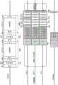
图1解说本公开在蜂窝电话100的示例实现中的各方面。蜂窝电话100可包括用户输入组件,诸如触摸屏102、按钮104等。蜂窝电话100内是底板106,其在图1中以放大视图解说以示出细节。底板106可以是例如其上附连有各组件的印刷电路板。例如,中央处理单元(CPU)108和存储器110可以被附连到底板106。CPU 108可以负责蜂窝电话100的通用处理任务,诸如在触摸屏102上显示图形用户界面,处理来自触摸屏和按钮104的用户输入,运行操作系统等。专门任务可以由其他组件执行,诸如专用集成电路(ASIC)112a-d。例如,ASIC112a-d可包括用于处理GPS信息的GPS ASIC,用于处理触摸感测数据的触摸ASIC等。CPU108和ASIC 112a-d可以通过总线114彼此通信。FIG. 1 illustrates aspects of the present disclosure in an example implementation of a
处置RF传输和接收的任务可以由RFIC 118和BBIC 120执行。RFIC 118和BBIC120可以通过信号线122彼此通信,信号线122可以是例如底板106上的金属迹线。RFIC118可以连接到天线124以将由天线接收到的RF信号处理成下行链路数据并且将上行链路数据处理成要由天线传送的RF信号。BBIC 120可以连接到总线114以与底板106上的其他系统通信以便例如将下行链路数据路由到恰适的系统,对要被传送的上行链路数据排定优先级并进行调度等。The tasks of handling RF transmission and reception may be performed by
图1包括RFIC 118和BBIC 120的放大视图。RFIC 118可包括物理层(PHY)组件(在此处被简称为“PHY”)(诸如PHY 130)、数据链路层(DLL)组件(在此处被简称为“DLL”)(诸如DLL 132)、分组接口(PKTIF)134、模数/数模(ADC/DAC)转换器136、以及RF区段138。RF区段138可以连接到天线124。在其他实施例中,天线可以与RF区段集成。BBIC 120可包括PHY140、DLL 142以及互连桥144。放大视图示出信号线122可包括一个或多个上行链路(UL)信号线150和一个或多个下行链路(DL)信号线152。FIG. 1 includes enlarged views of
对于下行链路通信,即蜂窝电话100从外部源(诸如蜂窝塔、GPS卫星等)接收通信,RF区段138可以处理通过天线接收到的模拟RF信号(下行链路信号),并且ADC/DAC转换器135可以将经处理的模拟下行链路信号转换成数字下行链路信号。分组接口134可以将数字下行链路信号分组化为数据分组。分组化是在计算机化的通信环境中向数据提供保护、标识、路由信息等的方式。例如,报头可以被包括在数据分组中以指示目的地地址,循环冗余校验(CRC)可以被添加到数据分组以在传输期间提供针对错误的保护等。分组接口134根据由互连桥144用于通过总线114进行数据传输的通信协议对下行链路信号进行分组化。该通信协议被附连到底板106的所有组件用于通过总线114进行通信。然而,在来自分组接口134的数据分组能够抵达互连桥144并且通过总线114被传送之前,数据分组必须通过下行链路信号线152从RFIC 118传送到BBIC 120。For downlink communications, ie
跨下行链路信号线152的通信可以由不同的协议(即串行链路协议)管控。DLL 132和PHY 130可以进一步根据该串行链路协议对下行链路数据进行分组化。PHY 130可以跨下行链路信号线152传送被进一步分组化的数据。PHY 140可以接收被进一步分组化的数据,PHY 140和DLL 142可以对数据分组进行去分组化,并且互连桥144可以通过总线114传送数据分组。Communication across
类似地,对于上行链路通信,即蜂窝电话100向外部源传送通信,互连桥144可以通过总线114接收上行链路数据分组。DLL 142和PHY 140可以根据串行链路协议对上行链路数据分组进一步分组化,并且PHY 140可以跨上行链路信号线150传送上行链路数据分组。PHY 130可以接收上行链路数据分组,并且PHY 130和DLL 132可以对数据分组进行去分组化。分组接口134可以进一步对上行链路数据分组去分组化为上行链路信号,以使得信号能够被RF区段138正确地传送。ADC/DAC转换器136可以从分组接口134接收上行链路信号,将这些数字信号转换成模拟信号,并且将模拟上行链路信号发送到RF区段138以进行传送。RF区段138可以处理要通过天线124被传送的模拟RF信号。Similarly, for uplink communications, ie,
根据本文公开的某些方面,提供了一种高级数字串行接口。该数字串行接口可以被实现在例如基带与移动通信设备等中的RF集成电路之间。According to certain aspects disclosed herein, an advanced digital serial interface is provided. The digital serial interface may be implemented, for example, between a baseband and an RF integrated circuit in a mobile communication device or the like.
在各实施例中,数字串行接口可以基于物理层(诸如以上的PHY 130与PHY 140)之间的单向时钟信号来进行传送和接收。单向时钟信令可以例如有助于减小串行链路的功耗。下面参考图2-5描述单向时钟信令的各方面的示例。In various embodiments, the digital serial interface may transmit and receive based on a unidirectional clock signal between physical layers such as
在各实施例中,数字串行接口可包括串行链路协议,该串行链路协议被工程设计以优化RF和基带功能从而提供高速、低功率串行链路通信。下面参考图8-12描述此类串行链路协议的各方面的示例。In various embodiments, the digital serial interface may include a serial link protocol engineered to optimize RF and baseband functionality to provide high speed, low power serial link communications. Examples of aspects of such serial link protocols are described below with reference to Figures 8-12.
此外,各实施例可包括串行链路的物理层(诸如以上的PHY 130和/或PHY 140)中的可编程分布式数据处理器。可编程分布式数据处理器可以向原本固定的链路架构增加灵活性同时维持低功率操作。下面参考图33-37描述此类可编程分布式数据处理器的各方面的示例。Furthermore, various embodiments may include a programmable distributed data processor in the physical layer of the serial link, such as
此外,各实施例可包括用于测试串行链路的嵌入式功能性。在一些实施例中,嵌入式测试可以部分地由可编程分布式数据处理器执行。下面参考图38-41描述嵌入式测试的各方面的示例。Additionally, embodiments may include embedded functionality for testing serial links. In some embodiments, embedded testing may be performed in part by a programmable distributed data processor. Examples of aspects of embedded testing are described below with reference to Figures 38-41.
图2解说基于单向时钟信令跨高速串行链路传送和接收信号的收发机装置200的示例。以此方式,例如,时钟信令电路系统的功耗与使用两个时钟相比可以较低。单向时钟信号可以被用于通过串行链路在主设备与从设备之间的通信的同步。就此,收发机装置200可包括链路从设备202和链路主设备204。链路主设备204将时钟信号(CLK)205发送到链路从设备202,并且高速串行链路上链路主设备与链路从设备之间的通信是基于CLK 205的。然而,链路从设备202不会向链路主设备204发送要用于高速串行链路上的通信的时钟信号。这是单向时钟信令的示例。2 illustrates an example of a
如此处所使用的,单向时钟信令由串行链路的一侧向串行链路的另一侧发送时钟信号来定义,其中串行链路上的通信是基于时钟信号的,并且该另一侧不会发送跨串行链路的通信所基于的时钟信号。同样,如此处所使用的,术语“单向时钟信号”指的是在单向时钟信令中被发送的时钟信号。As used herein, one-way clock signaling is defined by one side of a serial link sending a clock signal to the other side of the serial link, where communication on the serial link is based on the clock signal, and the other One side does not send the clock signal on which the communication across the serial link is based. Also, as used herein, the term "one-way clock signal" refers to a clock signal that is sent in one-way clock signaling.
收发机装置200可包括RF区段206。RF区段206可包括与RF信号的传输和接收有关的各种电路系统。例如,RF区段106可包括一个或多个天线。附加地,RF区段206可包括一个或多个RF滤波器或其他RF处理电路。收发机装置200还可包括ADC/DAC208,其可以被用于在ADC/DAC 208的ADC部分中将从RF区段206接收到的RF信号(模拟)转换成数字信号。例如,RF信号可以在RF区段206中在天线处接收。接收到的RF信号可以在RF区段206中被滤波或以其他方式被处理。接收到的RF信号(在诸如RF区段206中进行的滤波之类的任何RF处理之后)接着可以使用ADC/DAC 208中的ADC被转换成数字信号。如图2所解说的,在一些示例中,RF信号可以直接地而非在基带处从RF信号被转换成数字信号,或者从数字信号被转换成RF信号。接收到的RF信号的数字版本接着可以使用收发机装置20的其余部分进行数字化处理。
ADC/DAC 208还可在ADC/DAC的DAC部分中将数字信号转换成模拟信号。例如,由ADC/DAC 208从分组接口(PKTIF)210接收到的数字信号可以使用ADC/DAC的DAC部分被转换成RF信号(模拟)。由ADC/DAC 208从PKTIF 210接收到的数字信号的RF版本接着可以通过滤波或其他RF处理作为RF被处理。由ADC/DAC 208从PKTIF 210接收到的数字信号的RF版本可以使用RF区段206的一个或多个天线来传送。ADC/
图2解说了可以在链路从设备202与ADC/DAC 208之间传送的各个信号。例如,最终要使用RF区段206的一个或多个天线来传送的数字信号可以使用图2中解说的发射前端(TxFE)信号从PKTIF 210来发送。要由收发机装置200的剩余部分进一步处理的数字信号可以使用图2中解说的接收前端(RxFE)信号从ADC/DAC 208发送到PKTIF210。ADC/DAC 208可以经由图2中解说的反馈接收机(FBRx)信号向PKTIF 210提供反馈。在包括定位/位置功能性的通信系统中,ADC/DAC 208还可使用图2中解说的全球导航卫星系统信号(GNSS)将GNSS信号提供给收发机装置200的剩余部分。FIG. 2 illustrates various signals that may be communicated between link slave device 202 and ADC/
PKTIF 210可以被耦合到DLL 212,并且DLL 212可以向PKTIF提供对上行链路数据的访问。相反,DLL 212可以向链路物理编码子层(PCS)214提供对下行链路数据的访问。就此,链路PCS 214可以是驻留在串行化器-解串行化器(SERDES)收发机216顶部的链路协议子层以提供DLL 212与SERDES收发机216之间的接口。PCS 214和SERDES收发机216一起构成了链路从设备202的PHY 217。
SERDES收发机216可以从链路PCS 214接收下行链路数据,串行化下行链路数据,并且经由下行链路信号线219将串行下行链路数据传送到链路主设备204的SERDES收发机218。SERDES收发机216还可经由上行链路信号线220从SERDES收发机218接收串行上行链路数据,可以解串行化上行链路数据,并且可以将经解串行化的上行链路数据发送到链路PCS214。如上所述,链路主设备204与链路从设备202之间的该高速串行通信可以基于单向时钟信令。在该示例中,链路主设备204可以经由SERDES收发机218与216之间的串行链路将时钟信号205提供给链路从设备202。在一些实施例中,从链路主设备到链路从设备的时钟信号可以经由其他信道(诸如边带通信)来提供。
SERDES收发机218可以耦合到链路PCS 221。类似于链路PCS 214,链路PCS 221可以是驻留在SERDES收发机218顶部的链路协议子层以提供链路主设备204的SERDES收发机218与DLL 222之间的接口。PCS 221和SERDES收发机218一起构成了链路从设备202的PHY223。DLL 222可以将下行链路数据提供给互连桥224,并且互连桥可以将上行链路数据提供给DLL 222。互连桥224可以连接到其他设备,可以从这些其他设备接收UL数据并且可以向这些其他设备发送DL数据。在各实施例中,单向时钟信令可以提供若干优点。例如,通过消除一个或多个时钟来减少组件的数量能够减少引脚计数和所需的端口,这进而能够减少设备所驻留的印刷电路板上所要求的线缆数目。更少的组件还可减小IC面积并且降低噪声环境。在各实施例中,单向时钟信令可以有助于减小高速串行链路操作所需的功率。
收发机装置200还可包括其他功率节省功能性。例如,链路主设备204可以发起低功率模式,在低功率模式中链路主设备和链路从设备202进入低功率状态。在低功率状态中,SERDES收发机216和218不进行传送。当链路从设备202需要唤醒链路主设备204时,链路从设备可以使用可经由边带被发送到链路主设备的链路请求(link_req)信号226(即,不经由SERDES 216与218之间的串行链路)。同样地,链路主设备204可以使用链路使能(link_en)信号228(其可以是低有效信号)以使得设备间链路从设备202能够恢复串行链路通信。
图3解说了根据各实施例的基于单向时钟信令传达高速串行数据的串行互连300的示例SERDES收发机配置。串行互连300可包括充当从设备的SERDES收发机302以及充当主设备的SERDES收发机304。例如,在一些实施例中,图2的SERDES收发机216和218可以分别作为从设备302和主设备304来操作。3 illustrates an example SERDES transceiver configuration for a
在一些应用中,带宽要求不是对称的。换言之,针对一个方向中的数据流相比于另一方向中的数据流可能要求较高带宽。例如,蜂窝电话用户通常下载的数据比他们上传的数据多得多。因此,蜂窝通信系统中下行链路数据带宽使用通常远高于上行链路带宽使用。在这些情景中,可以通过利用使用3个DL通道310、312、314以及1个UL通道316来提供相比于上行链路带宽更多的下行链路带宽。每一个通道可执行数据的串行到并行(S2P)转换,数据的并行到串行(P2S)转换,时钟恢复,以及相关联的功能。此外,每一个通道可以使用生成时钟、偏置和启动序列的共同块。In some applications, the bandwidth requirements are not symmetrical. In other words, higher bandwidth may be required for data flow in one direction than for data flow in the other direction. For example, cellular phone users typically download much more data than they upload. Consequently, downlink data bandwidth usage is typically much higher than uplink bandwidth usage in cellular communication systems. In these scenarios, more downlink bandwidth than uplink bandwidth can be provided by utilizing the use of 3
通道由一个差分信令对构成,无论是用于UL话务还是用于DL话务。因而,每一个通道由两个线缆、信号迹线、导电通路等构成。例如,DL通道310包括两个线缆340和342。DL通道310还包括从设备302处的发射机330和P2S组件334,以及主设备304处的接收机332、S2P组件336和时钟/数据恢复(CDR)组件338。发射机330通过两个线缆340和342将信息发送到接收机332。P2S组件334将信息从并行转换成串行格式以便由发射机330串行地传送。S2P组件336将由接收机332接收到的串行信息转换成并行格式以供进一步处理。CDR组件338执行时钟/数据恢复。A channel consists of a differential signaling pair, either for UL traffic or for DL traffic. Thus, each channel consists of two cables, signal traces, conductive paths, and the like. For example,
串行互连300可以被配置成生成数据链路层分组以供将信息传输到第二设备。生成数据链路层分组以供将信息传输到第二设备可包括执行下文参考图12的1202描述的操作。生成数据链路层分组以供将信息传输到第二设备可以由与主设备304或从设备302相关联的处理器执行。
串行互连300可以被配置成将数据链路层分组封装在一个或多个物理层帧内。将数据链路层分组封装在一个或多个物理层帧内可包括执行下文参考图12的1204描述的操作。将数据链路层分组封装在一个或多个物理层帧内可以由与主设备304或从设备302相关联的处理器执行。
串行互连300可以被配置成将一个或多个物理层帧传送到第二设备。将一个或多个物理层帧传送到第二设备可以在下文参考图12的1206描述的操作中执行。将一个或多个物理层帧传送到第二设备可以由P2S组件(例如334)、发射机(例如330)或线缆(例如340和342)执行。
串行互连300可以被配置成从第二设备接收时钟信号。从第二设备接收时钟信号可以由从时钟块322或时钟接收机350执行。传送一个或多个物理层帧可包括基于时钟信号进行操作。传送可进一步包括抑制时钟信号到第二设备的传输。
串行互连300可以被配置成将时钟信号发送到第二设备。将时钟信号发送到第二设备可以由主时钟块320或时钟驱动器352执行。传送一个或多个物理层帧可包括基于时钟信号进行操作。
串行互连300可以被配置成抑制从第二设备接收时钟信号。抑制从第二设备接收时钟信号可以由主时钟块320或时钟驱动器352执行。
串行互连300可以被配置成从第二设备接收至少一个物理层帧。从第二设备接收至少一个物理层帧可包括执行下文参考图12的1208描述的操作。从第二设备接收至少一个物理层帧可以由S2P组件(例如336)、接收机(例如332)、CDR(例如338)、或线缆(例如340和342)执行。
串行互连300可以被配置成基于至少一个物理层帧获得一个或多个数据链路层分组。基于至少一个物理层帧获得一个或多个数据链路层分组可包括执行下文参考图12的1210描述的操作。基于至少一个物理层帧获得一个或多个数据链路层分组可以由与主设备304或从设备302相关联的处理器执行。
串行互连300可以被配置成基于一个或多个数据链路层分组提取数据或消息。基于一个或多个数据链路层分组提取数据或消息可包括执行下文参考图12的1212描述的操作。基于一个或多个数据链路层分组提取数据或消息可以由与主设备304或从设备302相关联的处理器执行。
关于时钟块介绍非对称性。为了改进解决方案的稳定性,串行互连300具有使主SERDES 304将时钟提供到从SERDES 302的同步操作。Asymmetry is introduced with respect to clock blocks. To improve the stability of the solution,
每一发射机串行化20比特并行接口。这通过具有可编程摆动电平的h桥驱动器来驱动。接收机能够访问线性均衡化。该设计提供了最大6Gbps的比特率。Each transmitter serializes a 20-bit parallel interface. This is driven by an h-bridge driver with programmable swing levels. The receiver has access to linear equalization. The design provides a maximum bit rate of 6Gbps.
串行互连300的SERDES取决于所要求的功率、性能和标准可支持以下功能:可编程Tx幅度;多个TX和Rx端接设置;多个功率状态;信号检测;广泛内置测试、可编程CDR开启和关断时间;用于快速频率切换的多个经校准锁相环(PLL)设置;多模BIST生成和BIST校验;用于测试数字电路系统的经复用扫描;多个回送;控制寄存器总线;直流联合测试行动小组(DC JTAG);与百万分之一(PPM)为单位的频率变动、码元间干扰(ISI)、以及有界不相关抖动(BUJ)相关联的片上抖动测试;用于Rx和Tx的20比特并行接口。
串行互连300的SERDES的一些规范为1e-16或更佳的误比特率(BER)(为达成该BER规范,对于板布局需要进行特别关注,例如,从RFIC到BBIC/从BBIC到RFIC的迹线的最大长度最大可以为6英寸,并且迹线的形状可以保持简单,例如,曲线可以被容忍,但尖角、通孔、连接器应当被最小化),所有通道可以以6Gbps在时钟缓冲器在功能模式中以3GHz运行的情况下来使用。Some specifications for the SERDES of the
在该单向时钟信令示例中,主SERDES 304中的时钟块320充当时钟发射机并且取得由PLL(高速模式、正常运行的)提供的时钟或由IC(低速模式)提供的内部时钟,并且生成所需的中间时钟并将中间时钟发送到主SERDES中的所有RX和TX块以及经由时钟驱动器352将半速率时钟发送到从设备302。In this one-way clock signaling example, the
在该单向时钟信令示例中,从SERDES 302中的时钟块322充当时钟接收机并且经由时钟接收机350接收由主设备304提供的时钟,生成所需的中间时钟并且将中间时钟发送到从SERDES 302中的所有RX和TX块。提供慢时钟模式(低速模式)以支持慢速操作。该模式可以例如在生产测试中使用以容纳测试员的限制。由于SERDES处置的高速信号,针对Tx和Rx缓冲器可能需要校准、端接设立。In this one-way clock signaling example, the
出于解说单向时钟信令的益处的目的,图3还示出与常规双向时钟信令相比不需要的一些组件399(组件399以虚线绘制以指示该组件不在本设计中)。具体地,单向时钟信令可允许在从SERDES侧消除PLL和时钟驱动器以及在主SERDES侧消除时钟接收机。组件399的消除可导致功率节省,因为所有这些组件都需要功率来运行。另外,组件399的消除可以减小串行互连300的芯片面积,从而允许串行互连变得更小。最终,组件399的消除可以减少连接串行互连300所要求的引脚数目、端口数目以及线缆数目。For purposes of illustrating the benefits of one-way clock signaling, FIG. 3 also shows some components 399 that are not required compared to conventional two-way clock signaling (component 399 is drawn in dashed lines to indicate that it is not in this design). Specifically, one-way clock signaling may allow for elimination of PLLs and clock drivers on the slave SERDES side and clock receivers on the master SERDES side. Elimination of components 399 may result in power savings since all of these components require power to operate. Additionally, the elimination of components 399 may reduce the chip area of
图4是根据各实施例的连接到串行链路的主设备(诸如图3的主SERDES 304)执行单向时钟信令的示例方法的流程图。主设备可以基于第一时钟生成(401)单向时钟信号,其中第一时钟是主设备中的时钟。例如,主SERDES 304可以基于主时钟块320来生成单向时钟信号。在一些实施例中,主设备可以生成与第一时钟相同速率的单向时钟信号。在一些实施例中,主设备可以生成是第一时钟速率的分数(例如半速率)的单向时钟信号。主设备可以将单向时钟信号发送(402)到连接至串行链路的从设备。例如,主SERDES304可以经由时钟驱动器352来传送单向时钟信号。在一些实施例中,主设备可以通过串行链路将单向时钟信号发送到从设备。在一些实施例中,主设备可以经由另一信道(诸如边带)将单向时钟信号发送到从设备。主设备可以基于第一时钟通过串行链路将数据传送(403)到从设备。例如,主SERDES 304可以基于主时钟块320通过UL通道316将数据传送到链路从SERDES 302。FIG. 4 is a flow diagram of an example method of performing one-way clock signaling by a master device connected to a serial link, such as
在一些实施例中,用于生成单向时钟信号的装置可包括第一时钟和可编程分布式数据处理器,在下文参考图33-37更详细地描述的。在其他实施例中,用于生成单向时钟信号的装置可包括控制链路的时钟信令的第一时钟和固定状态机。In some embodiments, the means for generating a unidirectional clock signal may include a first clock and a programmable distributed data processor, described in greater detail below with reference to Figures 33-37. In other embodiments, the means for generating a unidirectional clock signal may include a first clock and a fixed state machine that controls clock signaling of the link.
在一些实施例中,用于发送单向时钟信号的装置可包括SERDES收发机,诸如SERDES收发机218。在其他实施例中,用于发送单向时钟信号的装置可包括时钟驱动器,诸如时钟驱动器352。In some embodiments, the means for transmitting a unidirectional clock signal may include a SERDES transceiver, such as
在一些实施例中,用于通过串行链路将数据传送到从设备的装置可包括SERDES收发机,诸如SERDES收发机218。In some embodiments, the means for transmitting data to a slave device over a serial link may include a SERDES transceiver, such as
图5是根据各实施例的连接到串行链路的从设备(诸如图3的从SERDES 302)执行单向时钟信令的示例方法的流程图。从设备可以从连接到串行链路的主设备接收(501)单向时钟信号。例如,从SERDES 302可以经由时钟接收机350从主SERDES 304接收单向时钟信号。在一些实施例中,单向时钟信号可以通过串行链路接收。在一些实施例中,单向时钟信号可以经由另一信道(诸如边带)接收。从设备可以基于单向时钟信号通过串行链路将数据传送(502)到主设备。例如,从SERDES 302可以通过DL通道310将数据传送到主SERDES 304。在一些实施例中,从设备可以基于单向时钟信号来设置内部时钟,并且通过串行链路的数据传输可以基于该内部时钟。5 is a flow diagram of an example method of performing unidirectional clock signaling by a slave device connected to a serial link, such as
应当注意,物理层的逻辑子块(例如PCS)可以提供用于在DLL与电气子块(例如,SERDES收发机块)之间进行对接的装置,并且可以提供用于在将经封装的DLL分组发送到电气子块以供(例如通过信号线)传输之前进一步封装数据链路层分组的机制。逻辑子块可以在分组信息被封装成帧(例如,130比特帧)之前对跨所有可用通道被复用、条带化并且加扰的分组信息进行复用。It should be noted that logical sub-blocks (eg PCS) of the physical layer may provide means for interfacing between DLLs and electrical sub-blocks (eg, SERDES transceiver blocks) and may provide for grouping encapsulated DLLs A mechanism for further encapsulating data link layer packets before being sent to an electrical sub-block for transmission (eg, over a signal wire). The logical sub-blocks may multiplex the packet information that is multiplexed, striped, and scrambled across all available channels before the packet information is encapsulated into frames (eg, 130-bit frames).
逻辑子块可具有两个主区段:准备从数据链路层传递的传出信息以供由电气子块进行传输的发射区段;以及在将接收到的信息传递到数据链路层之前标识和准备接收到的信息的接收机区段。逻辑子块和电气子块可以通过状态和控制寄存器接口或等效的功能来协调每一收发机的状态。A logical sub-block may have two main sections: a transmit section that prepares outgoing information passed from the data link layer for transmission by the electrical sub-block; and an identification before passing received information to the data link layer and the receiver section of the information that is ready to be received. The logical and electrical sub-blocks may coordinate the state of each transceiver through a state and control register interface or equivalent functionality.
串行互连的物理层可以使用128b/130b编码方案,这可以将开销限于每数据帧1.5%(相比于例如通过使用8b/10b编码所要求的20%开销)。帧大小是130单元区间(UI)。每一UI包含1比特信息。在130比特中,2比特携带帧同步码元,并且其余128比特携带数据码元(即128b/130b编码)。UI可以是用于传输1比特信息的恒定时间区间(UI是比特率的逆。在6Gbps,1UI=0.16ns)。帧可以是130比特(1个帧可以在单个通道中在130个UI中传送,并且帧可以包含128比特信息和2比特同步码元)。块可以是130比特乘以每通道的比特数目(1个块可以在130个UI中传送(在抗偏斜之后),并且该块可以每个通道包含128比特信息和2比特同步码元)。同步码元可以是2比特(同步码元可以在每一物理层帧开始处周期性地传送,并且同步码元可以被用于在物理层消息收发以及数据链路层消息收发之间进行区分,例如,01可以标识分组猝发帧(数据链路层通信)而10可以标识PHY猝发帧(物理层通信))。Serially interconnected physical layers may use a 128b/130b encoding scheme, which may limit the overhead to 1.5% per data frame (compared to, for example, the 20% overhead required by using 8b/10b encoding). The frame size is 130 unit intervals (UI). Each UI contains 1 bit of information. Of the 130 bits, 2 bits carry frame synchronization symbols, and the remaining 128 bits carry data symbols (ie, 128b/130b encoding). UI may be a constant time interval for transmitting 1 bit of information (UI is the inverse of bit rate. At 6Gbps, 1UI=0.16ns). A frame may be 130 bits (1 frame may be transmitted in 130 UIs in a single channel, and a frame may contain 128 bits of information and 2 bits of synchronization symbols). A block may be 130 bits times the number of bits per channel (1 block may be transmitted in 130 UIs (after de-skew), and the block may contain 128 bits of information and 2 bits of synchronization symbols per channel). The synchronization symbol may be 2 bits (the synchronization symbol may be transmitted periodically at the beginning of each physical layer frame, and the synchronization symbol may be used to distinguish between physical layer messaging and data link layer messaging, For example, 01 may identify a packet burst frame (data link layer communication) and 10 may identify a PHY burst frame (physical layer communication)).
在一些实施例中,用于从连接到串行链路的主设备接收单向时钟信号的装置可包括SERDES收发机,诸如SERDES收发机216。在其他实施例中,用于从连接到串行链路的主设备接收单向时钟信号的装置可包括时钟接收机,诸如时钟接收机350。在一些实施例中,用于基于单向时钟信号通过串行链路将数据传送到主设备的装置可包括SERDES收发机,诸如SERDES收发机216。In some embodiments, the means for receiving a unidirectional clock signal from a master connected to the serial link may include a SERDES transceiver, such as
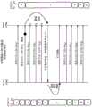
图6是解说在串行互连系统602上执行的示例操作600的图示。串行互连系统602可以例如为BBIC提供访问RFIC存储器和寄存器的低等待时间机制。BBIC主设备606可以最多向连贯的RFIC控制/状态寄存器(CSR)612写入1024比特数据。类似地,BBIC主设备606可以请求最多1024比特的连贯RFIC CSR位置612的读传递。所有RFIC 604发起的读和写传递跨串行互连系统602使用确保可靠传递的基于信用的流控机制来传递。FIG. 6 is a diagram illustrating
串行互连系统602提供调制解调器系统中RFIC 604与BBIC 606之间的全双工接口(上行链路和下行链路)。串行互连系统602的协议定义了数据和控制信息以分组化格式的传输。串行互连系统602的控制器实现该协议。串行互连系统602的SERDES提供高速串行传输机制。
串行数据在上行链路和下行链路方向上通过一个或多个通道来传输。所有数据通道同步操作并且共享同一标称带宽。串行链路的发射机侧与接收机侧之间的同步通过从BBIC 606发送到RFIC 604的共享时钟608来确保。使用单向时钟信号可以减小通过串行链路的数据传输和接收的功率,例如,因为少需要一个PLL。使用单向时钟信号还可减少设备所需的引脚数目。Serial data is transmitted over one or more channels in the uplink and downlink directions. All data channels operate synchronously and share the same nominal bandwidth. Synchronization between the transmitter side and receiver side of the serial link is ensured by a shared clock 608 sent from
在典型的基带中,下行链路数据话务要求比上行链路数据话务更多的带宽。由于带宽随着通道数目线性地缩放,因此带宽要求可以通过提供一个以上的数据通道来满足。In a typical baseband, downlink data traffic requires more bandwidth than uplink data traffic. Since bandwidth scales linearly with the number of channels, bandwidth requirements can be met by providing more than one data channel.
下行链路数据话务表示从天线接收到的、由RFIC 604中的ADC转换的、经滤波的、经下采样的、以及通过串行互连系统602被发送到BBIC 606的数据样本。存在多个独立的数据路径614,即接收机前端(RXFE)以及全球导航卫星系统(GNSS)内的经聚集载波。上行链路数据话务通过发射机前端(TXFE)数据路径,其具有比聚集下行链路数据路径总体上更低的带宽要求。串行互连系统602仅仅涉及数据的源和目的地,因此传入和传出数据缓冲器在串行互连系统602外部。所有数据经由统一接口被呈现给串行互连系统602。数据话务是实时话务。Downlink data traffic represents data samples received from the antennas, converted by ADCs in
除了数据话务,串行互连系统602还支持控制话务,控制话务包括访问RFIC 604上的存储器和CSR位置。尽管控制话务被给予高于数据话务的优先级,但对RFIC CSR 612的控制访问并不保证是固定等待时间的。In addition to data traffic,
除了数据和控制话务,串行互连系统602还提供用于交换流控和中断消息的链路层消息收发机制。串行互连系统602中的消息不是直接由更上层来访问,并且由串行互连系统602的数据链路层整体消费。In addition to data and control traffic,
图7是解说被优化以用于调制解调器芯片组、尤其用于BBIC与RFIC之间的通信的高带宽、低等待时间串行互连系统702的示例的图示。串行互连系统702被优化以实现低成本、低功率和低误比特率。串行互连系统702的主要目的是跨链路传递数据,包括BBIC706与RFIC 704之间的上行链路(UL)710与下行链路(DL)708。数据源和目的地点作为FIFO接口被呈现给串行互连系统702。串行互连系统702负责确保使用基于令牌的流控机制和重试的跨链路的可靠数据交换。FIG. 7 is a diagram illustrating an example of a high bandwidth, low latency
现在将参考8-12描述被工程设计以优化RF和基带功能以提供高速、低功率串行链路通信的串行链路协议。Serial link protocols that are engineered to optimize RF and baseband functions to provide high speed, low power serial link communications will now be described with reference to 8-12.
图8是解说实现串行互连系统800的分层模型的图示。串行互连系统800可以是例如上文参考图1和2描述的串行链路。串行互连系统800使用分组来在各个层之间传达信息。分组被形成在分组化层802中以携带来自发射机(Tx)组件810中的数据源的信息或者去往接收机(Rx)组件812中的数据阱的信息。当所传送的分组流经链路层804和物理层806时,这些分组用在那些层处处置分组所必需的附加信息来封装。在接收侧,反向过程发生,并且分组从它们的物理层806和链路层804表示转变为能够被接收方设备的分组化层802处理的形式。FIG. 8 is a diagram illustrating a layered model for implementing
分组化层802负责以下功能:在用于每一逻辑端点的I/Q流和固定长度分组流之间进行转换;管理每一UL/DL分组的源/目的地地址;以及发出与每一UL/DL分组相关联的读/写请求。DLL 804负责以下功能:添加分组报头;添加用于CRC的冗余比特;跨串行链路追踪分组的流控信用;管理分组确收(ACK)和重试消息;DLL分组错误的错误校验、错误处置、错误报告;以及处置功率状态转换。
PHY 806被分成两个子块:逻辑子块814和电气子块816,即SERDES。PHY逻辑子块814负责以下功能:将DLL分组包装成块和帧/解除DLL分组的包装;SERDES的均衡和同步猝发的插入;向DLL分组流增加物理层帧化令牌;对DLL分组和PING PHY猝发加扰和解扰;在接收机处实施PHY层帧化规则;以及接收到的比特流的帧化和对齐。SERDES 816负责以下功能:在传送方设备处将并行数据转换成串行数据;以及在接收方设备处将串行数据转换成并行数据。
在一种配置中,串行互连系统800包括具有每个通道最大6Gbps原始带宽的串行接口。PLL的输出频率可以是可编程的。源同步时钟可以被用于串行互连系统800中的所有UL和DL通道。主SERDES具有PLL,并且将时钟转发给从SERDES。串行互连系统800可包括双数据率(DDR)时钟。对于6Gbps数据率,DDR时钟可以是最大3GHz时钟。串行互连系统800可包括针对RF减敏的扩频控制(SSC)支持(例如,中心扩频或下扩频)。串行互连系统800包括在空闲时段期间的功率节省状态。串行互连系统800的功率状态的范围可以从轻度睡眠到深度睡眠,从而提供不同级别的功率/退出等待时间折中。In one configuration,
在一种配置中,串行互连系统800的PCS可以使用128b/130b编码方案,其具有比由传统串行互连系统使用的8b/10b编码更低的开销编码。串行互连系统800使用2比特同步码元,这使得用于确定分组边界的帧化同步码元最小化。In one configuration, the PCS of the
在一种配置中,在进入和退出功率节省状态之际,串行互连系统800使用简单且稳健的消息收发(例如,针对链路训练定义的模式、加扰器操作、转换到低功率状态等)。串行互连系统800可以采用多通道操作。串行互连系统800可以使用通道条带化,其中跨所有可用通道来发送数据以获得针对分组猝发模式中的猝发错误的最优带宽利用率和稳健性。In one configuration, the
在一种配置中,分组报头可包含信道标识(ID),其由CRC保护。串行互连系统的错误检测消除了分组路由到错误目的地的风险,并且触发重试机制。链路ID指定了每一端点的路由信息。In one configuration, the packet header may contain a channel identification (ID), which is protected by a CRC. Error detection for serial interconnect systems eliminates the risk of packets being routed to the wrong destination and triggers a retry mechanism. The link ID specifies routing information for each endpoint.
可以为数据样本和CSR访问分配多个链路ID。串行互连系统800可包括边带通信,例如,每一个方向上提供用于重置/唤醒以及错误恢复的机制的一个边带信号。串行互连系统800可包括ping模式。Ping操作将PHY和DLL层处的误比特率(BER)剖析分开。Multiple link IDs can be assigned for data samples and CSR access.
DLL负责跨串行链路可靠地传输消息和数据分组。DLL可以执行数据交换。例如,DLL可以接受供传输的分组并且将它们传达到物理层。DLL还可以接受通过物理层接收的分组并且将分组传达到目的地。DLL可以执行错误检测和重试。例如,DLL可以为所有DLL分组执行分组序列号管理。DLL还可以为所有DLL分组增加CRC保护。DLL可以执行分组的数据完整性校验。例如,DLL可以生成肯定和否定确收。DLL还可以生成用于错误报告和日志机制的错误指示。The DLL is responsible for the reliable transmission of messages and data packets across the serial link. DLL can perform data exchange. For example, a DLL may accept packets for transmission and communicate them to the physical layer. The DLL may also accept packets received through the physical layer and communicate the packets to the destination. The DLL can perform error detection and retry. For example, a DLL may perform packet sequence number management for all DLL packets. DLLs can also add CRC protection to all DLL packets. The DLL can perform data integrity checking of packets. For example, a DLL can generate positive and negative acknowledgements. The DLL can also generate error indications for error reporting and logging mechanisms.
串行互连系统800可包括两种类型的DLL分组:数据分组或消息分组。数据分组可以被用于数据传递以及对RFIC CSR的读和写。消息分组可以包含跨串行链路在DLL层之间交换的消息。消息分组可以被用于事件信令和流控消息收发。
串行互连系统800中(来自从设备)的DL话务的示例可包括以双字为单位指定目的地地址、写数据(最大1024比特)和长度的RFIC从写请求事务、对应于先前(UL子链路上)BBIC读请求的读响应数据、从RFIC DLL实体到BBIC DLL实体以用于BBIC的事件(EVT)消息的消息、以双字为单位指定源地址和长度的RFIC读请求(RD_REQ)消息,以及去往BBIC DLL实体的流控消息。串行互连系统800中(去往从设备)的UL话务的示例可包括:对应于在DL子链路上由RFIC发出的读请求(RD_REQ)消息的读响应数据,以双字为单位指定目的地地址、写数据(最大1024比特)和长度的BBIC写请求,从BBIC DLL实体到RFIC DLL实体的消息,诸如用于RFIC的事件(EVT)消息,以及以双字为单位指定源地址和长度的BBIC读请求(RD_REQ)消息;EVT,以及去往RFIC DLL实体的流控消息。An example of a DL traffic (from a slave device) in the
串行互连系统800上的所有DLL传递由分组构成。All DLL transfers on the
图9是解说由串行链路的DLL形成的两种类型的固定长度分组的示例分组结构的图示。这两种类型的分组是消息(MSG)分组910(同样也被称为DLL控制分组)和数据分组920。9 is a diagram illustrating an example packet structure for two types of fixed length packets formed by a DLL of a serial link. The two types of packets are message (MSG) packets 910 (also referred to as DLL control packets) and
MSG分组910具有56比特的固定长度,包括24比特报头、16比特有效载荷以及16比特CRC。MSG分组910的有效载荷可以被用于控制串行链路的各方面,并且有效载荷因此可以被称为控制消息。一旦DLL对控制消息分组化,经分组化的控制消息就可以被称为DLL控制分组(即,在DLL层经分组化的控制消息)。The
数据分组920具有1080比特的固定长度,包括24比特报头、1024比特有效载荷以及16比特CRC。在各实施例中,消息和数据分组可以是独立的,并且可以在用于传输的链路上被复用,并且向MSG分组给予优先级。这可允许高优先级消息(诸如事件(EVT))以最小的延迟进行传送。
在下面的表1中描述根据各实施例的示例分组格式:An example packet format according to various embodiments is described in Table 1 below:
表1分组格式Table 1 Grouping Format

每一分组具有消息区段和数据区段。消息和数据分组由16比特CRC保护。Each packet has a message section and a data section. Messages and data packets are protected by a 16-bit CRC.
下面在表2中描述根据各实施例支持的不同消息类型:The different message types supported according to various embodiments are described below in Table 2:
表2消息类型编码Table 2 Message Type Coding
下面在表3中描述根据各实施例支持的不同数据传递类型:The different data transfer types supported according to various embodiments are described below in Table 3:
表3数据类型Table 3 Data Types
下面在表4中描述根据各实施例支持的不同数据/消息子类型:The different data/message subtypes supported according to various embodiments are described below in Table 4:
表4消息子类型编码Table 4 Message subtype encoding
DLL层定义了每一方向中最多16个逻辑端点。每一端点被分配固定的“链路_id”。与端点相关联的所有分组使用该“链路_id”。带有1与15之间的链路_id的所有数据分组作为一类块传递来进行处理。具有被设为0的链路_id的数据分组被用于CSR读和写。与来自其他端点的数据分组相比,CSR访问在链路上被给予高优先级。下面在表5中描述根据各实施例支持的不同链路标识符:The DLL layer defines up to 16 logical endpoints in each direction. Each endpoint is assigned a fixed "link_id". All packets associated with the endpoint use this "link_id". All data packets with link_id between 1 and 15 are processed as a class of block transfers. Data packets with link_id set to 0 are used for CSR read and write. CSR access is given high priority on the link compared to data packets from other endpoints. The different link identifiers supported according to various embodiments are described below in Table 5:
表5链路标识符Table 5 Link identifiers

DLL在每一子链路上为流控使用序列号。消息(MSG)和数据(DATA)分组使用分开的序列号。序列号通过发射机被添加到每一分组并且由接收机进行校验。The DLL uses sequence numbers for flow control on each sublink. Message (MSG) and data (DATA) packets use separate sequence numbers. A sequence number is added to each packet by the transmitter and checked by the receiver.
图10是解说根据各实施例的PHY处的示例分组猝发结构的图示。如图所示,在PHY,来自DLL的MSG分组910可以通过在前方添加8比特MPT令牌1002被进一步分组化以创建MSG分组1001,MSG分组1001可以被称为PHY控制分组。因而,MSG分组1001的总长度为64比特(即8比特MPT令牌1002长度加上56比特MSG分组910长度)。10 is a diagram illustrating an example packet burst structure at a PHY in accordance with various embodiments. As shown, at the PHY, the
类似地,8比特DPT令牌1004被置于来自DLL的数据分组920(1080比特)前面以形成数据分组1003。因而,数据分组1003的总大小为1088比特。Similarly, an 8-
图11是解说根据各实施例的在具有双消息帧化的物理层处的消息和数据分组的示例128/130b编码的图示。在图11中示出的128b/130b编码中,两个MSG分组1001恰好能够容适进单个130比特的PHY帧1101中。换言之,128b/130b编码的封装长度是128比特,这恰好是PHY控制分组(即,MSG分组1001)长度的两倍。这一双消息帧化能够有助于提升消息传输的效率。具体来说,在其中消息被给予高优先级的系统中,在任何给定时间不会有超过两个消息在传输时隙队列中进行等待。11 is a diagram illustrating example 128/130b encoding of message and data packets at the physical layer with dual message framing, in accordance with various embodiments. In the 128b/130b encoding shown in FIG. 11, two MSG packets 1001 can just fit into a single 130-bit PHY frame 1101. In other words, the encapsulation length of 128b/130b encoding is 128 bits, which is exactly twice the length of the PHY control packet (ie, MSG packet 1001). This dual message framing can help improve the efficiency of message transmission. Specifically, in systems where messages are given high priority, no more than two messages will be waiting in the transmit slot queue at any given time.
如图11所示,物理层处的编码包括通过在第一MSG分组1001a的前面添加2比特分组猝发同步码元1102来形成帧,第一MSG分组1001a被置于第二经封装MSG分组1001b的前面以形成130比特的PHY帧1101。PHY帧1101可以在所有有效载荷空间被填充之后被立即发送,因为两个64比特MSG分组恰好容适到PHY帧的128比特封装长度中。As shown in Figure 11, encoding at the physical layer consists of forming a frame by adding a 2-bit packet
图11还示出了被分组化为多个PHY帧1101b-n的单个数据分组1003,其中数据分组1003被分成多个部分并且各个部分被插入多个连贯的PHY帧1101b-n中。如图11所示,PHY帧1101b包括同步码元1102以及DPT、数据报头、以及数据分组1003的数据有效载荷的一部分。PHY帧1101c-n中的每一者包括同步码元1102以及数据分组1003的数据有效载荷的一部分。PHY帧1101n包括同步码元1102、以及数据有效载荷的最后一部分和数据分组1003的CRC,它们没有填充PHY帧1101n的整个128比特封装长度。因此,PHY帧1101n具有容适更多数据或消息的附加空间。Figure 11 also shows a
串行互连系统允许在处于分组猝发模式中时跨多个通道子链路的字节条带化(也被称为数据交织)。在一个以上通道上传送的数据被交织,这意味着传递中的每一字节在连贯的通道中被发送。本公开将此类交织称为字节条带化。条带化要求附加的硬件复杂度来对传入的经条带化字节进行抗偏斜,但是条带化可以按照与分组猝发的传递长度以及正被用于数据传递的通道数成比例的方式来显著地缩短等待时间。The serial interconnect system allows byte striping (also known as data interleaving) across multiple channel sub-links when in packet burst mode. Data transmitted on more than one channel is interleaved, which means that each byte in the transmission is sent in a coherent channel. This disclosure refers to such interleaving as byte striping. Striping requires additional hardware complexity to de-skew incoming striped bytes, but striping can be done in proportion to the transfer length of the packet burst and the number of lanes being used for data transfer way to significantly reduce waiting time.
图12是执行串行点到点互连的方法的流程图。该方法可以由第一设备执行,诸如图2的链路从设备202或链路主设备204。在1202,第一设备生成数据链路层分组以供将信息传输到第二设备。在一种配置中,DLL分组可以由图6的链路层604基于上文参考图9描述的分组结构来生成。12 is a flowchart of a method of performing a serial point-to-point interconnect. The method may be performed by a first device, such as link slave device 202 or link master device 204 of FIG. 2 . At 1202, the first device generates a data link layer packet for transmission of information to the second device. In one configuration, the DLL packet may be generated by the
在1204,第一设备将数据链路层分组封装在一个或多个物理层帧内。在一种配置中,物理层帧可以由图6的物理层606基于上文参考图10描述的结构来生成。在一种配置中,一个或多个物理层帧中的每一者包括同步码元。同步码元长度与物理层帧长度之比可以为小于2到10。At 1204, the first device encapsulates the data link layer packet within one or more physical layer frames. In one configuration, the physical layer frame may be generated by the
在1206,第一设备将一个或多个物理层帧传送到第二设备。例如,第一设备可以是图2的链路从设备202,并且第二设备可以是图2的链路主设备204。在此类配置中,第一设备从第二设备接收时钟信号。例如,链路从设备202可以从链路主设备204接收时钟信号205。一个或多个物理层帧的传送可以基于时钟信号。时钟信号是单向的。因而,第一设备抑制时钟信号到第二设备的传输。At 1206, the first device transmits one or more physical layer frames to the second device. For example, the first device may be the link slave device 202 of FIG. 2 and the second device may be the link master device 204 of FIG. 2 . In such a configuration, the first device receives the clock signal from the second device. For example, link slave device 202 may receive clock signal 205 from link master device 204 . The transmission of one or more physical layer frames may be based on a clock signal. The clock signal is unidirectional. Thus, the first device suppresses the transmission of the clock signal to the second device.
在1208,第一设备从第二设备接收至少一个物理层帧。在1210,第一设备例如通过图6的链路层604中的处理基于至少一个物理层帧获得一个或多个数据链路层分组。在1212,第一设备基于一个或多个数据链路层分组提取数据或消息。At 1208, the first device receives at least one physical layer frame from the second device. At 1210, the first device obtains one or more data link layer packets based on at least one physical layer frame, eg, by processing in
在一种配置中,数据链路层分组是供数据传递的数据分组。数据分组的长度是1080比特,并且数据分组包括24比特报头、1024比特有效载荷以及16比特CRC。在一种配置中,数据链路层分组是用于事件信令和流控消息收发的消息分组。消息分组的长度是56比特,并且消息分组包括24比特报头、16比特有效载荷以及16比特循环冗余校验(CRC)。In one configuration, the data link layer packets are data packets for data transfer. The length of the data packet is 1080 bits, and the data packet includes a 24-bit header, a 1024-bit payload, and a 16-bit CRC. In one configuration, the data link layer packets are message packets used for event signaling and flow control messaging. The length of the message packet is 56 bits, and the message packet includes a 24-bit header, a 16-bit payload, and a 16-bit Cyclic Redundancy Check (CRC).
在一种配置中,所有消息分组可以跨单个虚拟消息信道来进行流传输,并且所有数据分组可以通过虚拟数据信道来进行流传输。在此类配置中,虚拟消息信道和虚拟数据信道可以使用独立的流控机制。虚拟消息信道针对流控可以采用隐式确收,而虚拟数据信道可以采用基于信用的流控。In one configuration, all message packets may be streamed across a single virtual message channel, and all data packets may be streamed over the virtual data channel. In such a configuration, the virtual message channel and virtual data channel may use independent flow control mechanisms. The virtual message channel can use implicit acknowledgment for flow control, while the virtual data channel can use credit-based flow control.
在一种配置中,每一物理层帧是130比特长,并且包括2比特同步码元。2比特同步码元在数据链路层分组之外。2比特同步码元可指示物理层的两种操作模式之一:分组猝发或物理层猝发。分组猝发被用于第一设备与第二设备之间的数据链路层通信。物理层猝发被用于物理层通信。在一种配置中,至少一个物理层帧可进一步包括8比特令牌,其使用于分组猝发的分组类型差异化并且使用于物理层猝发的物理层通信类型差异化。在一种配置中,物理通道帧在一个或多个物理通道上被传送或接收。In one configuration, each physical layer frame is 130 bits long and includes 2-bit synchronization symbols. The 2-bit sync symbol is outside the data link layer packet. The 2-bit sync symbol may indicate one of two modes of operation of the physical layer: packet burst or physical layer burst. Packet bursts are used for data link layer communication between the first device and the second device. Physical layer bursts are used for physical layer communications. In one configuration, the at least one physical layer frame may further include an 8-bit token that differentiates the packet type used for the packet burst and the physical layer communication type used for the physical layer burst. In one configuration, physical channel frames are transmitted or received on one or more physical channels.
图13是解说根据各实施例的在具有双消息帧化的物理层处编码消息和数据分组的示例协议的方法的流程图。图13的方法可以例如由上述RFIC或BBIC来执行。设备可以是生成(1301)DLL控制分组以供将控制消息传输到第二设备。例如,DLL控制分组可以是图9的MSG分组910。每一DLL控制分组可具有DLL控制分组长度,DLL控制分组长度是固定长度。例如,MSG分组910的固定长度是56比特。设备生成(1302)PHY控制分组。每一PHY控制分组包括DLL控制分组和控制令牌之一。每一PHY控制分组的长度是DLL控制分组长度与控制令牌的控制令牌长度之和。例如,PHY控制分组可以是图10的MSG分组1001,其包括56比特MSG分组910和8比特MPT令牌1002,总长度为64比特。设备将PHY控制分组封装(1303)在帧中。每一帧包括具有码元长度的同步码元。每一帧的长度是码元长度和封装长度之和,并且封装长度是PHY控制分组长度的两倍。例如,PHY帧1101包括2比特的同步码元1102,并且在128比特的封装长度中进一步包括两个64比特MSG分组1001。设备将帧传送(1304)到第二设备。在一些实施例中,封装长度与每一帧的长度之比是64/65,例如,在上述的128b/130b编码中。13 is a flowchart illustrating a method of an example protocol for encoding messages and data packets at a physical layer with dual message framing in accordance with various embodiments. The method of Figure 13 may be performed, for example, by the RFIC or BBIC described above. The device may be to generate (1301) a DLL control packet for transmission of the control message to the second device. For example, the DLL control packet may be the
在一些实施例中,同步码元指示用于PHY的两种操作模式之一。操作模式包括用于设备与第二设备之间的数据链路层通信的分组猝发,以及用于物理层通信的物理层猝发。在一些实施例中,DLL控制分组长度是56比特,并且控制令牌长度是8比特。In some embodiments, the synchronization symbol indicates one of two modes of operation for the PHY. The modes of operation include packet bursting for data link layer communication between the device and the second device, and physical layer bursting for physical layer communication. In some embodiments, the DLL control packet length is 56 bits and the control token length is 8 bits.
在一些实施例中,设备可进一步生成DLL数据分组以供将数据传输到第二设备,其中通过来自存储器的读请求来获得数据,读请求返回固定数据长度的数据。此外,每一DLL数据分组可包括数据有效载荷,数据有效载荷具有的数据有效载荷长度是读请求所返回的数据的数据长度的倍数。设备可以生成PHY数据分组,其中每一PHY数据分组包括一个DLL数据分组和数据令牌,并且设备可以将PHY数据分组封装在帧中。在一些实施例中,数据有效载荷长度是1024比特。In some embodiments, the device may further generate a DLL data packet for transmission of the data to the second device, wherein the data is obtained by a read request from the memory, the read request returning data of a fixed data length. Additionally, each DLL data packet may include a data payload having a data payload length that is a multiple of the data length of the data returned by the read request. The device may generate PHY data packets, where each PHY data packet includes a DLL data packet and a data token, and the device may encapsulate the PHY data packets in frames. In some embodiments, the data payload length is 1024 bits.
用于生成DLL控制分组以供将控制消息传输到第二设备的装置可包括DLL,诸如DLL 212和222。The means for generating the DLL control packet for transmission of the control message to the second device may include a DLL, such as
用于生成物理层(PHY)控制分组的装置可包括PHY,诸如PHY 217和223。The means for generating physical layer (PHY) control packets may include PHYs, such as
用于将PHY控制分组封装在帧中的装置可包括PHY,诸如PHY 217和223。The means for encapsulating PHY control packets in frames may include PHYs, such as
在一些实施例中,用于将帧传送到第二设备的装置可包括SERDES收发机,诸如SERDES收发机216和218。In some embodiments, the means for transmitting the frame to the second device may include a SERDES transceiver, such as
图14是解说根据各实施例的用于串行互连系统的示例流控机制的图示。数据(DATA)传递1420实现块确收机制,其中一旦话务类的信用已经被耗尽,就发送ACK MSG1422。接收机还将每一DATA分组的序列号进行比较,并且如果接收机检测到非预期序列号就向DLL发送否定确收(NACK)消息。14 is a diagram illustrating an example flow control mechanism for a serial interconnect system in accordance with various embodiments. Data (DATA)
MSG分组1410的确收策略略有不同。所有MSG分组共享一个共同的序列号。接收机隐式地确收每一MSG分组,并且仅在接收机检测到MSG分组的序列号错误的情况下才发送重试消息。在最后一个正确接收的MSG之后的所有消息必须被接收机丢弃并且被发射机重试。链路层控制(LLC)可以维护足够深的消息缓冲器以覆盖在传送方和接收方DLL实体之间的最差情形的往返延迟。The acknowledgment strategy of
串行互连系统是RFIC与BBIC之间的点到点通信信道。ACK消息被用于进行基于信用的流控通信。流控在帧包的MSG和DATA信道之间独立地进行。消息(MSG)和数据(DATA)信道使用独立的流控机制。所有读请求事件消息和其他消息分组跨单个虚拟消息信道来仲裁和流传输。所有写请求和读响应分组跨DATA虚拟数据信道来仲裁和流传输。链路id字段被用于在数据和CSR访问之间进行区分。将所有数据话务编组到单个信用ACK队列中允许更高效的缓冲器管理以及更低的ACK响应开销。将CSR访问作为单独的话务类来处理能够通过避免由于数据分组引起的线头阻塞来实现跨串行链路的控制话务的低等待时间的传递。The serial interconnect system is a point-to-point communication channel between the RFIC and the BBIC. ACK messages are used for credit-based flow control communications. Flow control is performed independently between the MSG and DATA channels of the frame packet. The message (MSG) and data (DATA) channels use independent flow control mechanisms. All read request event messages and other message packets are arbitrated and streamed across a single virtual message channel. All write request and read response packets are arbitrated and streamed across the DATA virtual data channel. The link id field is used to differentiate between data and CSR access. Grouping all data traffic into a single credit ACK queue allows for more efficient buffer management and lower ACK response overhead. Treating CSR access as a separate traffic class enables low latency delivery of control traffic across serial links by avoiding head-of-line blocking due to data packets.
串行互连系统可以使用基于信用的流控来确保在分组能够跨链路被发送之前,接收方侧具有接受该分组的足够缓冲器空间。如先前所述,互连的两侧交换MSG和DATA分组。MSG和DATA是独立的,它们必须对串行链路上的传送接入进行仲裁。在上电或重置之际,传输信用被初始化到最大值。每一次从RFIC传送数据分组到BBIC,RFIC应当减小其DATA信道信用。BBIC将处理数据分组并且周期性地向RFIC传送ACK MSG以确收所有正确接收的DATA分组。在接收到ACK消息之际,RFIC更新其信用计数器。类似的机制适用于CSR DATA信道。Serial interconnect systems can use credit-based flow control to ensure that the receiver side has enough buffer space to accept a packet before it can be sent across the link. As previously described, both sides of the interconnect exchange MSG and DATA packets. MSG and DATA are independent and must arbitrate for transmission access on the serial link. On power-up or reset, transfer credits are initialized to a maximum value. Each time a data packet is transmitted from the RFIC to the BBIC, the RFIC shall decrease its DATA channel credit. The BBIC will process the data packets and periodically transmit an ACK MSG to the RFIC to acknowledge all correctly received DATA packets. Upon receipt of the ACK message, the RFIC updates its credit counter. A similar mechanism applies to the CSR DATA channel.
作为对比,MSG传递1410不必采用基于信用的ACK方案。取而代之,所有MSG分组被假定为被正确接收。只要接收方DLL实体发现非预期MSG序列号,就发送NACK消息。In contrast,
为了数据和控制信息的稳健交换,两种机制可以被内置于DLL分组中。每一DLL分组具有16比特CRC,并且一旦接收到分组,就针对预期CRC校验CRC。而且,MSG部分和DATA部分两者都携带8比特的(序列号)Seq_num字段,当分组在发射机侧组装时该字段在MSG和DATA信道上独立地递增和维护;并且接收机侧校验接收到的MSG/DATA Seq_num以确保没有丢失的MSG或DATA。只要检测到CRC错误或脱序MSG/DATA Seq_num,接收机侧会向发射机侧报告错误状态。在接收到该错误报告之际,发射机侧将尝试重新发送MSG/DATA。For robust exchange of data and control information, two mechanisms can be built into the DLL packet. Each DLL packet has a 16-bit CRC, and once the packet is received, the CRC is checked against the expected CRC. Also, both the MSG part and the DATA part carry an 8-bit (sequence number) Seq_num field, which is incremented and maintained independently on the MSG and DATA channels when the packet is assembled at the transmitter side; and the receiver side checks the reception to the MSG/DATA Seq_num to ensure no missing MSG or DATA. Whenever a CRC error or out-of-sequence MSG/DATA Seq_num is detected, the receiver side reports an error status to the transmitter side. Upon receipt of this error report, the transmitter side will attempt to resend the MSG/DATA.
该错误报告和重试机制可能要求发射机侧在那些MSG/DATA已经被发送之后也保留MSG/DATA的缓冲器,以防链路上发生错误而它们没有被成功接收。另一方面,当MSG/DATA被成功接收并且推送进入iMSG/iDATA缓冲器1414/1424时,接收机侧可以向发射机侧报告,以使得发射机侧可以释放由那些MSG/DATA占据的位置并且释放其eMSG/eDATA缓冲器1412/1422上的空间。在串行互连的两侧具有足够的eMSG和eDATA缓冲器并且在两侧对iMSG或iDATA缓冲器的出栈都具有很少的回推时,流控(FC)消息可用作对正确接收的MSG/DATA的保守且频繁的状态报告,并且发射机侧可能仅仅需要保留信用_指针(Credit_ptr)与写_指针(Wr_ptr)之间的内容。This error reporting and retry mechanism may require that the transmitter side also keep a buffer of MSG/DATA after those MSG/DATA have been sent, in case errors occur on the link and they are not successfully received. On the other hand, when MSG/DATA are successfully received and pushed into iMSG/
特殊消息类型NACK被定义为用于报告收到分组的错误以及用于请求重试。在表6中解说根据各实施例的NACK消息的示例定义:A special message type NACK is defined for reporting errors in received packets and for requesting retry. Example definitions of NACK messages according to various embodiments are illustrated in Table 6:
表6NACK消息定义Table 6 NACK message definition

为了确保NACK消息被传达到另一侧,每一个生成的NACK消息可能经受三重传输保护:发射机将同一NACK消息传送三次;并且接收机可以组合和合并三个连贯的NACKMSG以形成重试动作。如果CRC在三个NACK消息中的任一者上失败,则失败的有效载荷将被丢出并且在有效载荷组合时不被使用。To ensure that NACK messages are communicated to the other side, each generated NACK message may be subject to triple transmission protection: the transmitter transmits the same NACK message three times; and the receiver may combine and combine three consecutive NACKMSGs to form a retry action. If the CRC fails on any of the three NACK messages, the failed payload will be dropped and not used when the payloads are combined.
图15是解说根据各实施例的MSG信道上的NACK消息和重试过程的示例的图示。DATA信道上的NACK消息被类似地处置。注意,一旦远程DLL实体检测到一个收到分组上的错误,则同一信道上的之后的分组将不会被推送进入iMSG/iDATA缓冲器,直到NACK消息的三次传输完成,并且稍后接收到的MS/DATA是正确的且具有与最后被推送的MSG/DATA连续的序列号(seq_num)为止。15 is a diagram illustrating an example of a NACK message and retry procedure on an MSG channel in accordance with various embodiments. NACK messages on the DATA channel are handled similarly. Note that once the remote DLL entity detects an error on a received packet, subsequent packets on the same channel will not be pushed into the iMSG/iDATA buffer until three transmissions of the NACK message are complete and the later received MS/DATA is correct and has a sequence number (seq_num) consecutive to the last pushed MSG/DATA.
在此示例中,串行互连的接收机侧的去分组化器1503提取序列号为4的MSG。在该MSG上检测到错误。接收机侧接着生成NACK消息以指示序列号等于4的MSG上的错误。在接收到NACK消息之际,发射机侧将读_指针(Rd_ptr)倒回指向MSG 4以进行重试/重传。In this example, the serially interconnected receiver side depacketizer 1503 extracts the MSG with
图15中描述的NACK/重试过程可以保护串行互连两侧交换的基本消息和数据。然而,如果包含FC消息的分组上发生错误,则FC消息没有重试,因为它们在传输期间不被推送进入eMSG缓冲器中。为了保护包括FC消息的混合消息,可以添加以下协议:如果一侧检测到分组上的错误并且发出NACK消息,在NACK消息正被传送的同时,该侧仍然需要处理正确接收的FC消息(如果存在);当相对侧接收到NACK消息时,该相对侧应当通过立即传输FC消息来作出响应。图16-20在下文解说了该NACK-FC重试协议。The NACK/retry process described in Figure 15 protects the essential messages and data exchanged on both sides of the serial interconnect. However, if an error occurs on the packet containing the FC message, the FC message is not retried because they are not pushed into the eMSG buffer during transmission. To protect mixed messages including FC messages, the following protocol can be added: if one side detects an error on the packet and issues a NACK message, while the NACK message is being delivered, that side still needs to process the correctly received FC message (if there is one) ); when the opposite side receives a NACK message, the opposite side shall respond by transmitting an FC message immediately. 16-20 illustrate the NACK-FC retry protocol below.
图16是解说根据各实施例的成功数据传输的示例的图示。在该示例中,在BBIC1604处成功接收数据分组0-3之际,BBIC向RFIC 1602发送消息分组0。消息分组0指示BBIC1604已经接收到数据分组0-3,并且在BBIC 1604处要接收的下一数据分组的预期序列号为4。16 is a diagram illustrating an example of a successful data transfer in accordance with various embodiments. In this example, upon successful receipt of data packets 0-3 at
图17是解说根据各实施例的下行链路数据传输上的错误和重试的示例的图示。在该示例中,RFIC 1702将数据分组6-10按顺序发送到BBIC 1704。在数据分组7的传输期间,发生比特错误(例如,CRC失配或非预期序列号)。作为对数据分组7上的比特错误的响应,BBIC 1704丢弃接收到的数据分组8-10,并且发送NACK消息以指示数据分组7上的错误。在RFIC 1702处接收到NACK消息之际,RFIC将FC消息发送到BBIC1704。稍后,RFIC 1702将数据分组7-10重新发送到BBIC 1704。17 is a diagram illustrating an example of errors and retries on downlink data transmission in accordance with various embodiments. In this example,
图18是解说根据各实施例的成功上行链路消息传输的示例的图示。在该示例中,在RFIC 1802处成功接收消息分组9和10之际,RFIC向BBIC 1804发送消息分组1。消息分组1指示RFIC 1802已经接收到最多序列号为10的消息分组,并且在RFIC 1802处要接收的下一消息分组的预期序列号为11。18 is a diagram illustrating an example of a successful uplink message transmission in accordance with various embodiments. In this example, upon successful receipt of
图19是解说根据各实施例的上行链路消息传输上的错误和重试的示例的图示。在该示例中,BBIC 1904将消息分组9-11按顺序发送到RFIC 1902。在消息分组10的传输期间,发生比特错误(例如,CRC失配或非预期序列号)。作为对消息分组10上的比特错误的响应,RFIC 1902丢弃接收到的消息分组11,并且发送NACK消息以指示消息分组10上的错误。在BBIC 1904处接收到NACK消息之际,BBIC将FC消息发送到RFIC1902。稍后,BBIC 1904将消息分组10和11重新发送到RFIC 1902。在RFIC 1902处成功接收消息分组10和11之际,RFIC将消息分组n+1发送到BBIC 1904。消息分组n+1指示RFIC 1902已经接收到最多序列号为11的消息分组,并且在RFIC 1902处要接收的下一消息分组的预期序列号为12。19 is a diagram illustrating an example of errors and retries on uplink message transmission in accordance with various embodiments. In this example,
图20是解说根据各实施例的流控消息上的错误以及错误触发的重试的示例的图示。在该示例中,RFIC 2002在消息分组6和7之间将FC消息分组发送到BBIC 2004。在FC消息分组的传输期间,发生比特错误(例如,CRC失配)。响应于FC消息上的比特错误,BBIC 2004丢弃接收到的消息分组7和8,并且发送NACK消息以指示FC消息分组上的错误。在RFIC 2002处接收到NACK消息之际,RFIC将FC消息发送到BBIC 2004。稍后,RFIC 2002将消息分组7和8重新发送到BBIC 2004。20 is a diagram illustrating an example of errors on flow control messages and error-triggered retries, according to various embodiments. In this example,
图21是解说根据各实施例的写事务序列的示例的图示。WR_REQ发起该序列,数据信道的ACK_RESP指示WR_REQ被接收到并且数据被发布以被提交到目的地。为所有DL DATA传输维持单个流控信用,并且单个流控信用被用于所有UL DATA事务。21 is a diagram illustrating an example of a sequence of write transactions in accordance with various embodiments. The WR_REQ initiates the sequence and the ACK_RESP of the data channel indicates that the WR_REQ was received and the data was released to be committed to the destination. A single flow control credit is maintained for all DL DATA transmissions, and is used for all UL DATA transactions.
图22是解说根据各实施例的读事务序列的示例的图示。读事务作为具有类型RD_REQ、RD_RESP对以及RD_DATA、RD_DATA_RESP对的拆分事务来处理。每一类型对维持具有ACK方案的单独的流控。由于消息和数据总是按顺序被接受,因此这允许拆分事务内的每一对被独立地追踪。在此示例中,拆分事务被示为在时间上分开的2对,并且每一对在错误处置和重试方面被分开地处置。22 is a diagram illustrating an example of a read transaction sequence in accordance with various embodiments. Read transactions are handled as split transactions with pairs of type RD_REQ, RD_RESP and pairs of RD_DATA, RD_DATA_RESP. Each type pair maintains separate flow control with an ACK scheme. Since messages and data are always accepted in order, this allows each pair within a split transaction to be tracked independently. In this example, a split transaction is shown as 2 pairs separated in time, and each pair is handled separately in terms of error handling and retries.
RD_REQ发起序列;RD_RESP指示RD_REQ已经被接收到。当RD_REQ被接收到时,响应方还激活RD_DATA。一旦从源检索到读数据,读数据就作为数据分组(RD_DATA)被发送。当RD_DATA被接收到时,RD_DATA_RESP被发送回。用于RD_REQ、RD_RESP以及RD_DATA、RD_DATA_RESP的ACK和流控被分开处置。RD_REQ initiates the sequence; RD_RESP indicates that RD_REQ has been received. The responder also activates RD_DATA when RD_REQ is received. Once the read data is retrieved from the source, the read data is sent as a data packet (RD_DATA). When RD_DATA is received, RD_DATA_RESP is sent back. ACK and flow control for RD_REQ, RD_RESP and RD_DATA, RD_DATA_RESP are handled separately.
中断消息事务将具有INT消息类型,并且流控信用类似于RD_REQ。中断消息应当跨消息信道来仲裁和流传输。重试和错误处置机制与RD_REQ相同。功率管理消息被用于支持串行互连的功率状态事务。错误信令消息被用于用信号指示在特定事务上发生的错误以及不一定与特定事务相关联的错误。这些消息由检测到错误的代理来发起。Interrupt message transactions will have INT message type and flow control credits similar to RD_REQ. Interrupt messages should be arbitrated and streamed across message channels. The retry and error handling mechanism is the same as RD_REQ. Power management messages are used to support power state transactions for serial interconnects. Error signaling messages are used to signal errors that occurred on a particular transaction and errors that are not necessarily associated with a particular transaction. These messages are initiated by the agent that detected the error.
图23是根据各个实施例的处置接收到的分组的方法的流程图。该方法可以由设备(例如,本文描述的BBIC或RFIC)来执行。在一种配置中,当接收到的分组从接收数据链路层被递送到接收事务层时,在DLL已经验证了接收到的分组的完整性之后,接收到的分组通过该方法来处置。在2302,设备确定分组是否遵守格式。如果分组遵守格式,则设备前进到2304,否则前进到2306。23 is a flowchart of a method of handling a received packet in accordance with various embodiments. The method may be performed by a device (eg, a BBIC or RFIC as described herein). In one configuration, when the received packet is delivered from the receive data link layer to the receive transaction layer, the received packet is handled by this method after the DLL has verified the integrity of the received packet. At 2302, the device determines whether the packet follows the format. If the packet conforms to the format, the device proceeds to 2304, otherwise to 2306.
在2304,设备确定分组的类型值是否被定义。如果类型值被定义,则设备前进到2308,否则前进到2306。At 2304, the device determines whether the type value of the packet is defined. If the type value is defined, the device proceeds to 2308, otherwise to 2306.
在2306,设备确定分组是坏的,丢弃该分组,并且报告坏分组。该方法随后结束。At 2306, the device determines that the packet is bad, discards the packet, and reports the bad packet. The method then ends.
在2308,设备更新流控追踪。在2310,设备确定分组是否是请求。如果分组是请求,则设备处置该请求。如果分组不是请求,则分组是完成态并且设备处置该完成态。At 2308, the device updates the flow control tracking. At 2310, the device determines whether the packet is a request. If the packet is a request, the device handles the request. If the packet is not a request, the packet is completion and the device handles the completion.
图24是根据各个实施例的校验接收到的分组的错误的方法的流程图。该方法可以由设备(例如,BBIC或RFIC)的DLL来执行。在2402,设备确定PCS是否指示分组的任何接收到的错误。如果指示至少一个错误,则设备前进到2406,否则前进到2404。在2406,设备丢弃该分组。该方法随后结束。24 is a flowchart of a method of checking a received packet for errors in accordance with various embodiments. The method may be performed by a DLL of the device (eg, BBIC or RFIC). At 2402, the device determines whether the PCS indicates any received errors for the packet. If at least one error is indicated, the device proceeds to 2406, otherwise to 2404. At 2406, the device discards the packet. The method then ends.
在2404,设备使用接收到的不包括CRC字段的分组数据来计算CRC。在2408,设备确定计算所得的CRC是否等于分组中接收到的CRC。如果CRC匹配,则设备前进到2410,否则前进到2412。At 2404, the device calculates a CRC using the received packet data that does not include a CRC field. At 2408, the device determines whether the calculated CRC is equal to the CRC received in the packet. If the CRCs match, the device proceeds to 2410, otherwise to 2412.
在2410,设备处理该分组。该方法随后结束。在2412,设备丢弃该分组并且报告错误。该方法随后结束。At 2410, the device processes the packet. The method then ends. At 2412, the device discards the packet and reports an error. The method then ends.
图25是根据各个实施例的处置接收到的请求的方法的流程图。该方法可以由设备(例如,本文描述的BBIC或RFIC)来执行。在一种配置中,在关于所有事务层分组的初始处理之后,接收到的请求通过该方法来处置。在2502,设备确定请求类型是否被支持。如果请求类型被支持,则设备前进到2506,否则前进到2504。25 is a flowchart of a method of handling a received request in accordance with various embodiments. The method may be performed by a device (eg, a BBIC or RFIC as described herein). In one configuration, received requests are handled by this method after initial processing of all transaction layer packets. At 2502, the device determines whether the request type is supported. If the request type is supported, the device proceeds to 2506, otherwise to 2504.
在2504,设备识别出请求是不受支持的请求。在2508,设备确定请求是否要求完成。如果请求要求完成,则设备前进到2510,否则该方法结束。在2510,设备发送完成并且该方法结束。At 2504, the device identifies that the request is an unsupported request. At 2508, the device determines whether the request requires completion. If the request requires completion, the device proceeds to 2510, otherwise the method ends. At 2510, the device transmission is complete and the method ends.
在2506,设备确定请求类型是否是MSG。如果请求类型是MSG,则设备前进到2512,否则前进到2514。At 2506, the device determines whether the request type is MSG. If the request type is MSG, the device proceeds to 2512, otherwise to 2514.
在2512,设备确定MSG中的有效载荷是否被定义。如果MSG中的有效载荷被定义,则设备前进到2518,否则前进到2516。At 2512, the device determines whether the payload in the MSG is defined. The device proceeds to 2518 if the payload in the MSG is defined, otherwise proceeds to 2516.
在2516,设备处理该MSG。该方法随后结束。在2518,设备处理该MSG。该方法随后结束。At 2516, the device processes the MSG. The method then ends. At 2518, the device processes the MSG. The method then ends.
在2514,设备确定请求是否违背协议。如果请求违背协议,则设备前进到2522,否则前进到2520。At 2514, the device determines whether the request violates the protocol. If the request violates the protocol, the device proceeds to 2522, otherwise to 2520.
在2520,设备处理该请求。在2524,设备确定请求是否要求完成。如果请求要求完成,则设备前进到2526,否则该方法结束。在2526,设备发送完成并且该方法结束。At 2520, the device processes the request. At 2524, the device determines whether the request requires completion. If the request requires completion, the device proceeds to 2526, otherwise the method ends. At 2526, the device transmission is complete and the method ends.
在2520,设备确定请求是否要求完成。如果请求要求完成,则设备前进到2528,否则该方法结束。在2528,设备发送完成并且该方法结束。At 2520, the device determines whether the request requires completion. If the request requires completion, the device proceeds to 2528, otherwise the method ends. At 2528, the device transmission is complete and the method ends.
对于读请求,数据作为具有1024比特固定长度的数据分组来返回,无论读请求所请求的比特数是多少。数据分组报头中的长度字段指示由数据分组携带的有效字数:对于数据样本,有效载荷总是32个字(1024比特);而对于CSR事务,长度将以双字为单位来指示要被生成的猝发的大小。For read requests, data is returned as data packets with a fixed length of 1024 bits, regardless of the number of bits requested by the read request. The length field in the data packet header indicates the number of valid words carried by the data packet: for data samples, the payload is always 32 words (1024 bits); for CSR transactions, the length will be in double words to indicate the number of words to be generated. The size of the burst.
在任何拆分事务协议中,存在与请求方无法接收预期完成相关联的风险。为了允许请求方以标准方式从此情景中尝试恢复,定义了完成超时机制。该机制旨在仅在对于完成返回没有合理预期的情况下被激活,并且在正常操作状况下应当从不发生。In any split transaction protocol, there is a risk associated with the requestor not being able to receive the expected completion. To allow the requestor to attempt recovery from this scenario in a standard way, a completion timeout mechanism is defined. This mechanism is intended to be activated only when there is no reasonable expectation of a complete return, and should never happen under normal operating conditions.
串行互连系统的物理层实现以下功能:通过提供在PHY猝发(物理层通信)或DLL猝发之间进行区分的同步码元插入的128b/130b编码;从BBIC到RFIC的STMR同步;Rx通道帧对齐和多通道抗偏斜;均衡化;用于快速唤醒、休眠唤醒、初始引导和恢复的训练序列,涉及均衡化、CDR和对齐;物理层令牌插入,包括空闲链路(IDL);用于追踪PHY错误的物理层统计计数器的维护;低速(LS)模式和高速(HS)模式处置。PHY处置来自/进入能够被物理层和更上层进一步处理的数据块的SERDES数据的分组化和去分组化;加扰数据链路层通信(加扰可以被用于使EMI在串行互连上通过的信号的频率内容“白化”并且减小任何一个特定频率处的辐射功率,并且加扰可以在每个通道的基础上进行);跨活跃通道的字节数据的条带化和去条带化;以及SERDES与数据链路层(控制器)域之间的异步时钟交叉。The physical layer of the serial interconnect system implements the following functions: 128b/130b encoding by providing synchronization symbol insertion to differentiate between PHY bursts (physical layer communication) or DLL bursts; STMR synchronization from BBIC to RFIC; Rx channel Frame alignment and multi-lane anti-skew; equalization; training sequences for fast wakeup, sleep wakeup, initial boot and recovery involving equalization, CDR, and alignment; physical layer token insertion, including idle link (IDL); Maintenance of physical layer statistics counters for tracking PHY errors; low speed (LS) mode and high speed (HS) mode handling. PHY handles packetization and de-packetization of SERDES data from/to data blocks that can be further processed by the physical layer and higher layers; scrambling data link layer communications (scrambling can be used to make EMI over serial interconnect The frequency content of the passed signal "whitens" and reduces the radiated power at any one particular frequency, and scrambling can be done on a per-channel basis); striping and de-striping of byte data across active channels and asynchronous clock crossing between the SERDES and the data link layer (controller) domain.
图26解说了根据各实施例在一个通道配置中能够每130个UI(有效载荷内容可以改变)周期性地重复的示例时序图。128b/130b封装在物理层内处置。存在用于物理层的两种操作模式。每一操作模式由其自己的2比特同步报头来定义,该2比特同步报头定义了链路的具体操作模式。每一操作模式的令牌被附加到每一传递以进一步对跨链路发送的数据进行分类。第一操作模式是分组猝发,它被用于BBIC与RFIC之间的数据链路层通信。第二种类型的操作模式是PHY猝发,用于物理层通信。分组和通道之间的区分通过两个同步码元比特来完成:同步码元0x01指示分组猝发,而同步码元0x10指示PHY猝发。26 illustrates an example timing diagram that can be repeated periodically every 130 UIs (payload content may change) in a channel configuration in accordance with various embodiments. 128b/130b encapsulation is handled within the physical layer. There are two modes of operation for the physical layer. Each mode of operation is defined by its own 2-bit sync header that defines the specific mode of operation of the link. A token for each mode of operation is appended to each pass to further classify the data sent across the link. The first mode of operation is packet bursting, which is used for data link layer communication between the BBIC and the RFIC. The second type of operation mode is PHY burst, which is used for physical layer communication. The distinction between packets and lanes is accomplished by two synchronization symbol bits: synchronization symbol 0x01 indicates a packet burst, and synchronization symbol 0x10 indicates a PHY burst.
分组猝发被用于数据链路层通信。分组猝发可以包含数据、数据分组形式的配置数据、或中断、DLL通信、ACK/NACK、ping、以及消息形式的数据请求。分组猝发由2比特同步报头(0x01)来定义。8比特令牌对分组类型进行区分。令牌被置于每一传递的同步码元之后的第一字节中。在分组猝发中,同步码元不被加扰,而令牌和有效载荷总是被加扰。Packet bursts are used for data link layer communications. Packet bursts may contain data, configuration data in the form of data packets, or interrupts, DLL communications, ACK/NACK, ping, and data requests in the form of messages. Packet bursts are defined by a 2-bit sync header (0x01). The 8-bit token differentiates the packet type. The token is placed in the first byte after each transmitted sync symbol. In a packet burst, the synchronization symbols are not scrambled, while the token and payload are always scrambled.
分组猝发具有两个子类型:消息分组,包括中断、ACK/NACK、读请求、ping、以及DLL通信;以及数据分组,存储器映射传递、配置访问和IQ样本数据。Packet bursts have two subtypes: message packets, including interrupts, ACK/NACKs, read requests, pings, and DLL communications; and data packets, memory mapped transfers, configuration access, and IQ sample data.
分组猝发格式遵守这些规则:8比特的令牌被加扰并且受到三位翻转保护,有效载荷被加扰并且受CRC保护,而EPB令牌必须作为要切换到PHY猝发的指示来发送并且被要求是在切换到PHY猝发操作模式之前传送的最后一个字节,在该令牌与PHY猝发报头之间没有空闲。下文在表7中描述根据各实施例的分组猝发令牌的示例列表:The packet burst format obeys these rules: the 8-bit token is scrambled and protected by three-bit flips, the payload is scrambled and protected by CRC, and the EPB token must be sent as an indication to switch to PHY burst and required is the last byte transmitted before switching to PHY burst mode of operation, with no idle time between this token and the PHY burst header. An example list of packet burst tokens according to various embodiments is described below in Table 7:
表7分组猝发令牌的列表TABLE 7 List of Packet Burst Tokens

图27解说了根据各实施例的跨三个通道启用字节条带化2700以及禁用字节条带化2750的示例。在启用字节条带化2700中,传递中的每一字节在连贯通道中发送。例如,MPT令牌在通道0中发送,MPT令牌之后的第一字节在通道1中发送,MPT令牌之后的第二字节在通道2中发送,MPT令牌之后的第三字节在通道0中发送,并且以此类推。27 illustrates an example of enabling
加扰器能够显著降低连续的0或1的长扫描宽度的概率。加扰器还对功率频谱进行扩频,并且因而能够避免分立频率处的毛刺。The scrambler can significantly reduce the probability of long scan widths of consecutive 0s or 1s. The scrambler also spreads the power spectrum and is thus able to avoid spurs at discrete frequencies.
串行互连系统应当支持具有以下生成多项式的加扰器:Serial interconnect systems SHOULD support scramblers with the following generator polynomials:
G(X)=X23+X21+X16+X8+X5+X2+1G(X)=X23 +X21 +X16 +X8 +X5 +X2 +1
该加扰器的重复周期是224-1UI=16777215。只有数据字节应当被加扰,同步码元和令牌保持未加扰。帧中的比特数为128,重复周期因此是131072帧。The repetition period of the scrambler is 224 -1UI=16777215. Only the data bytes should be scrambled, the sync symbols and tokens remain unscrambled. The number of bits in a frame is 128 and the repetition period is therefore 131072 frames.
加扰器通过在PHY猝发结尾处的SPB令牌中使用特殊有效载荷来进行重置,加扰器将独立于每一字节上的数据而在每一字节上进行更新,除非在使用BSV PHY猝发的情况下。以此方式,发射机和接收机两者都应当从不失步。链路上可能发生比特错误,但假定发射机和接收机上的130比特数模式,LFSR应当总是匹配。一些示例配置包括:加扰器每个通道独立运作,且一个通道一个加扰器;加扰器在分组层数据和PHY传递BSV中使用;2比特同步码元、令牌和PHY猝发数据不被加扰;数据的每一字节被唯一的24比特LFSR值加扰;LFSR值被冻结并且在BSV PHY猝发期间被广播;令牌和同步码元在PHY猝发模式中从不被加扰,并且令牌在分组猝发模式中被加扰;SPB令牌上的特殊有效载荷重置加扰器,并且当错误导致发射机和接收机失步时使用该重置。The scrambler is reset by using a special payload in the SPB token at the end of the PHY burst, the scrambler will be updated on each byte independently of the data on each byte, unless using BSV In the case of PHY burst. In this way, both the transmitter and receiver should never lose synchronization. Bit errors can occur on the link, but assuming a 130-bit pattern on the transmitter and receiver, the LFSR should always match. Some example configurations include: scramblers operate independently per lane, and one scrambler per lane; scramblers are used in packet layer data and PHY pass BSV; 2-bit sync symbols, tokens, and PHY burst data are not used. Scrambling; each byte of data is scrambled by a unique 24-bit LFSR value; LFSR values are frozen and broadcast during BSV PHY bursts; tokens and sync symbols are never scrambled in PHY burst mode, and The token is scrambled in packet burst mode; a special payload on the SPB token resets the scrambler and is used when an error causes the transmitter and receiver to lose synchronization.
图28解说了数据分组格式2800和消息分组格式2850。字节1111_1111b指示数据分组传递(DPT)令牌。该令牌被用于对携带数据样本的数据分组、配置数据、DLL数据或RFIC与BBIC之间的其他存储器映射数据进行帧化。DPT大小为1088比特(8比特令牌+1080数据分组有效载荷)。数据分组有效载荷结构的细节在上文参考图9进行描述。28 illustrates a
字节0000_1111b指示消息分组传递(MPT)令牌。该令牌被用于将消息分组作为分组猝发的一部分进行帧化。消息分组传递被用于传送RFIC与BBIC之间的中断、ACK/NACK、读请求、ping、以及DLL通信。MPT大小为64比特(8比特令牌+56比特消息分组有效载荷)。消息分组有效载荷结构的细节在上文参考图9进行描述。Byte 0000_1111b indicates a message packet transfer (MPT) token. This token is used to frame message packets as part of a packet burst. Message packet delivery is used to convey interrupts, ACK/NACKs, read requests, pings, and DLL communications between RFIC and BBIC. The MPT size is 64 bits (8-bit token + 56-bit message packet payload). Details of the message packet payload structure are described above with reference to FIG. 9 .
字节0000_0000b指示空闲(IDL)链路令牌。空闲令牌在分组猝发期间使用以填充未被消息传递、数据传递或分组猝发传输期间分组猝发令牌结尾占据的间隙。该分组被加扰。Ping模式用于检测链路状态并且每个通道运行BER分析。空闲模式还用于跨链路上的所有通道发送已知有效载荷加扰序列,因为每一通道被要求具有带不同LFSR模式的单独加扰器逻辑,这种设置允许在每个个体通道上进行独立的错误剖析。Bytes 0000_0000b indicate an idle (IDL) link token. Idle tokens are used during packet bursts to fill gaps not occupied by the end of a packet burst token during message passing, data transfer, or packet burst transmission. The packet is scrambled. Ping mode is used to detect link status and run BER analysis per channel. Idle mode is also used to send known payload scrambling sequences across all lanes on the link, since each lane is required to have separate scrambler logic with a different LFSR mode, this setup allows on each individual lane Independent error profiling.
由1111_0000b表示的EPB令牌用于描述从数据链路层通信到物理层通信的切换。该令牌必须是在切换到物理层通信(PHY猝发操作模式)之前的最后一个数据字节。The EPB token represented by 1111_0000b is used to describe the handover from data link layer communication to physical layer communication. This token must be the last data byte before switching to physical layer communication (PHY burst mode of operation).
PHY猝发被用于物理层通信。PHY猝发可包含均衡化、CDR和对齐信息、指示分组猝发的开头、用信号指示传输的开头或结尾、跨链路发送统一计时器值并且提供供追踪工具追踪加扰器中的LFSR模式的方式。PHY bursts are used for physical layer communication. PHY bursts may contain equalization, CDR and alignment information, indicate the beginning of a packet burst, signal the beginning or end of a transmission, send uniform timer values across the link and provide a way for tracking tools to track LFSR patterns in the scrambler .
PHY猝发由2比特同步报头(0x10)来定义。8比特令牌对PHY层通信类型进行区分。令牌被置于每一传递的同步码元之后的第一字节中。在PHY猝发中,令牌或有效载荷均不加扰。A PHY burst is defined by a 2-bit sync header (0x10). The 8-bit token distinguishes the type of PHY layer communication. The token is placed in the first byte after each transmitted sync symbol. In a PHY burst, neither the token nor the payload is scrambled.
PHY猝发具有多种PHY到PHY通信的子类型:STS-系统计时器同步;SPB-分组猝发的开头;BSV-广播加扰器值;EOT-传输结尾;SOT-传输开头;SYNC-高速模式中CDR的开头;EQ-均衡化模式。PHY bursts have several subtypes of PHY-to-PHY communication: STS - System Timer Synchronization; SPB - Beginning of Packet Burst; BSV - Broadcast Scrambler Value; EOT - End of Transmission; SOT - Beginning of Transmission; SYNC - In High Speed Mode Beginning of CDR; EQ - equalization mode.
PHY猝发格式遵守这些规则:8比特令牌不被加扰;对于任何PHY猝发,有效载荷不被加扰;所有猝发由每个活跃通道1个数据帧(130比特)构成,除非可以是具有可变长度的BSV;多通道链路的所有通道必须同时传送带相同同步码元和令牌的帧;取决于传递类型,有效载荷将是每字节重复模式或三重冗余;SPB令牌必须作为从PHY猝发切换到分组猝发的指示来发送并且SPB令牌被要求是在切换到分组猝发操作模式之前传送的最后一个字节;对于BSV排序集的字节,LFSR不提前,对于所有其他字节LFSR被提前。The PHY burst format obeys these rules: 8-bit tokens are not scrambled; for any PHY burst, the payload is not scrambled; all bursts consist of 1 data frame (130 bits) per active Variable-length BSV; all lanes of a multi-lane link must simultaneously carry frames with the same synchronization symbols and tokens; depending on the type of delivery, the payload will be repeat-per-byte pattern or triple-redundant; SPB tokens must be used as slaves An indication of the PHY burst switching to packet burst is sent and the SPB token is required to be the last byte transmitted before switching to packet burst mode of operation; LFSR is not advanced for bytes of the BSV ordering set, LFSR for all other bytes be advanced.
下文在表8中示出根据各实施例的示例PHY猝发令牌列表:An example PHY burst token list according to various embodiments is shown below in Table 8:
表8PHY猝发令牌列表TABLE 8 PHY Burst Token List

2Dh定义STMR同步令牌(STS)。STMS同步传递被用于在BBIC与RFIC之间同步统一计时器值。所递送的值是三重冗余的,并且该值与STMR计数器的上采样相位P0一起发送进入RFIC以允许各组件之间的正确同步。2Dh defines the STMR synchronization token (STS). STMS synchronization transfer is used to synchronize uniform timer values between BBIC and RFIC. The delivered value is triple redundant and is sent into the RFIC along with the upsampling phase P0 of the STMR counter to allow proper synchronization between components.
E_1h指示分组猝发的开头(SPB)。该令牌被用于从PHY猝发转换到分组猝发模式和数据链路层通信。分组猝发的开头是在切换到分组猝发操作模式之前通道上发送的最后一个帧。E_1h indicates the start of a packet burst (SPB). This token is used for transitioning from PHY burst to packet burst mode and for data link layer communications. The beginning of a packet burst is the last frame sent on the channel before switching to the packet burst mode of operation.
广播加扰器值PHY猝发发送LFSR值以帮助追踪工具达成块对齐。该值以三重冗余的方式来发送。在BSV传递期间,每一字节上LFSR值不会提前,而在任何其他传递期间,LFSR会提前。BSV在每个通道的基础上提供LFSR加扰器值。Broadcast Scrambler Values The PHY sends LFSR values in bursts to help the tracking tool achieve block alignment. The value is sent in a triple redundant manner. During a BSV pass, the LFSR value is not advanced on each byte, and during any other pass, the LFSR is advanced. BSV provides LFSR scrambler values on a per-channel basis.
令牌66h指示PHY猝发操作模式期间传输的结尾。该令牌在发射机进入电气空闲之前被发送出去。EOT令牌的接收机应当忽略在EOT令牌已经被接收到之后的所有数据,直到接收到EQ、SYNC或SOT令牌。Token 66h indicates the end of the transmission during the PHY burst mode of operation. This token is sent out before the transmitter goes into electrical idle. The receiver of the EOT token should ignore all data after the EOT token has been received until an EQ, SYNC or SOT token is received.
传输的开头由具有低频0->1->0->1模式的帧来定界。该模式被用于在链路上启动任何其他非初始化话务之前的通道和块对齐。该模式还被用于在启动分组猝发模式操作之前重启加扰器逻辑。The beginning of the transmission is delimited by frames with a low frequency 0->1->0->1 pattern. This mode is used for lane and block alignment prior to initiating any other non-initialized traffic on the link. This mode is also used to restart the scrambler logic before initiating packet burst mode operation.
使用全部字节使用AAh模式的帧的同步模式被用于接收机进行的时钟和数据恢复。该帧将按链路需要尽可能多次地被发送出去。在低速模式中链路的第一次初始化期间,每一次链路被初始化时要发送的CDR帧数必须被配置。A sync pattern of frames using AAh pattern with all bytes is used for clock and data recovery by the receiver. The frame will be sent out as many times as the link requires. During the first initialization of the link in low-speed mode, the number of CDR frames to be sent each time the link is initialized must be configured.
均衡化模式被用于减少码元间干扰,并且允许链路中传送数据的可靠恢复。均衡化帧由A5h模式构成,该A5h模式使用加扰器的LFSR模式来帮助模拟电路系统以最优的方式完成均衡化过程。在均衡化规程期间要被发送的EQ帧数必须经由消息收发来编程。The equalization mode is used to reduce inter-symbol interference and allow for reliable recovery of transmitted data in the link. The equalization frame consists of an A5h pattern that uses the LFSR pattern of the scrambler to help the analog circuitry perform the equalization process in an optimal manner. The number of EQ frames to be sent during the equalization procedure must be programmed via messaging.
从帧到物理通道的映射规则是复杂的,以下解说了猝发映射到链路的物理通道的两个示例。在表10中,可以观察到分组猝发的映射。在以下的表9和10中,描绘了根据各实施例的示例PHY猝发:The mapping rules from frames to physical channels are complex, and two examples of burst mapping to physical channels of a link are explained below. In Table 10, the mapping of packet bursts can be observed. In Tables 9 and 10 below, example PHY bursts according to various embodiments are depicted:
表9分组猝发映射到物理通道TABLE 9 Mapping of packet bursts to physical channels


表10PHY猝发映射到物理级Table 10 PHY burst mapping to physical level


图29解说了根据各实施例的在单个物理通道209处的示例数据链路层和物理层传输。在该示例中,PHY猝发2910之后是分组猝发,分组猝发包括分组2904和2906。PHY猝发2910结束于SPB令牌2914,SPB令牌2914指示在将操作模式从PHY猝发切换到分组猝发之前的最后一个帧。存在在分组2904和2906之间传送的若干IDL令牌2916。分组2906之后是EPB令牌2918,EPB令牌2918指示从分组猝发到PHY猝发操作模式的切换。EPB令牌2918之后是PHY猝发2912,PHY猝发2912之后是包括分组2908的另一分组猝发。分组2908之后是EPB令牌2922,EPB令牌2922之后是EOT令牌2920,EOT令牌2920指示在将通道2902置于电气空闲之前的最后一个帧。29 illustrates example data link layer and physical layer transmissions at a single physical channel 209 in accordance with various embodiments. In this example, PHY burst 2910 is followed by a packet burst, which includes
图30解说了根据各实施例的在三个物理通道1-3处的示例数据链路层和物理层传输。在该示例中,物理通道1-3中的每一者开始于PHY猝发3010。对于PHY猝发3010中的每一帧,同步码元是“10”。PHY猝发3010之后是分组猝发3012。对于分组猝发3012中的每一帧,同步码元是“01”。分组猝发3012包括消息分组3001和三个数据分组3002-3004。分组字节在物理通道1-3上进行条带化。每一分组开始于一个令牌。例如,消息分组3001开始于MPT令牌3020,而数据分组3003开始于DPT令牌3022。在通道1-3中的每一者上,分组猝发3012之后是EOT令牌3026。30 illustrates example data link layer and physical layer transmissions at three physical channels 1-3 in accordance with various embodiments. In this example, each of physical lanes 1-3 begins with a
链路均衡化在上电之后链路的第一次启用期间完成。均衡化的目的在于减少码元间干扰以确保高速传送数据的可靠恢复。均衡化必须在每一次链路被下电并且被再次上电在高速模式中操作之前完成,并且在任何其他时间没有必要进行执行。在一种配置中,当处于PHY猝发模式中时,链路均衡化可以在任何时间进行。均衡化时间是可变的,并且取决于技术和过程偏斜而逐芯片且逐部件地改变。链路花费在均衡化规程中的时间量是可经由低速模式编程来配置的。当串行互连第一次在移动到任何其他高速状态之前从高速深度睡眠状态中苏醒时,可能需要进行均衡化。Link equalization is done during the first activation of the link after power-up. The purpose of equalization is to reduce inter-symbol interference to ensure reliable recovery of high-speed transmission data. Equalization must be done each time a link is powered down and powered up again to operate in high speed mode, and need not be performed at any other time. In one configuration, link equalization can occur at any time when in PHY burst mode. The equalization time is variable and varies from chip to chip and part to part depending on technology and process skew. The amount of time the link spends in the equalization procedure is configurable via low-speed mode programming. Equalization may be required when the serial interconnect first wakes up from a high-speed deep-sleep state before moving to any other high-speed state.
时钟数据恢复(CDR)序列调整每一通道的接收机设置以改进信号质量并且通过将时钟与数据眼的中心对齐来满足所要求的信号完整性。CDR必须在串行互连的第一次高速苏醒期间执行。即便在每一次从任何睡眠转换到活跃模式时不要求重复CDR以实现可靠操作,DLL仍然将具有在任何时间重复该规程的选项。在以下条件之后可能需要CDR:链路第一次从低速移动到高速操作;每一次从高速睡眠转换到高速猝发;每一次从高速深度睡眠中转换出来。The Clock Data Recovery (CDR) sequence adjusts the receiver settings for each channel to improve signal quality and meet the required signal integrity by centering the clock to the data eye. The CDR must be performed during the first high-speed wake-up of the serial interconnect. Even though repeating the CDR is not required for reliable operation on every transition from any sleep to active mode, the DLL will still have the option to repeat this procedure at any time. CDR may be required after: the first time the link moves from low speed to high speed operation; every transition from high speed sleep to high speed burst; every transition out of high speed deep sleep.
通道对齐被用于在数据已经被解串行化器处理以检测帧边界之后在接收机中可靠地构建数据。块对齐被用于通过检测链路中每一数据通道之间的恰适偏斜来可靠地构建逻辑数据。Lane alignment is used to reliably construct data in the receiver after it has been processed by the deserializer to detect frame boundaries. Block alignment is used to reliably construct logical data by detecting the proper skew between each data lane in the link.
图31解说了根据各实施例的可被用于追踪高速串行链路的状态的示例状态机。在设备上电3100,链路进入上电状态3101。链路可以转换到从设备检测状态3103。链路可以从从设备检测状态3103转换到配置状态3105。链路可以从配置状态3105转换到活跃状态3107。附加状态包括轻度睡眠状态3109、深度睡眠状态1311和恢复状态3113。状态之间的移动通过各种外部因素来确定,包括序列、外部输入和错误。31 illustrates an example state machine that may be used to track the state of a high-speed serial link in accordance with various embodiments. After the device is powered on 3100, the link enters the powered-on state 3101. The link may transition to the slave detection state 3103. The link may transition from the slave device detection state 3103 to the configuration state 3105. The link may transition from the configured state 3105 to the active state 3107. Additional states include
两个边带信号可以被用于控制串行互连的操作状态。这些信号可以是低速、主要为静态的信号,它们指示串行互连所处的状态和/或串行互连将移动到的状态。在一些实施例中,边带信号可以是如上参考图2描述的link_en和link_req。在该示例中,link_en可以从主设备(例如BBIC)发送到从设备(例如RFIC),并且可具有两种用途,第一种在冷引导时而第二种在标准操作期间。在冷引导时,从设备侧处的定序器可以使用ROM代码来遵循作为到从设备的输入定义的策略link_en来引导,link_en预期为‘0b。在link_en在上电重置(POR)时被设为‘1b的情形中,则正常引导序列将不会执行,并且从设备将进入“测试/调试”模式,并且基于POR时的通用输入/输出(GPIO)设置,RF前端(RFFE)或其他调试特征将被激活。在操作期间,RFIC可以是BBIC的从设备,并且SERDES PHY时钟可以由BBIC提供。从设备知晓SERDES时钟是否可用、准备好进行操作(意味着SERDES时钟能够被从SERCES PHY使用)的唯一方式是检测link_en上的‘1b。因此,遵循功率策略,主定序器将根据SERDES PHY时钟的状态来断言link_en。Two sideband signals can be used to control the operational state of the serial interconnect. These signals may be low-speed, primarily static signals that indicate the state the serial interconnect is in and/or the state the serial interconnect will move to. In some embodiments, the sideband signals may be link_en and link_req as described above with reference to FIG. 2 . In this example, link_en may be sent from a master (eg, BBIC) to a slave (eg, RFIC), and may have two purposes, the first during cold boot and the second during standard operation. At cold boot, the sequencer at the slave side can use the ROM code to boot following the policy link_en defined as an input to the slave, which is expected to be '0b. In the case where link_en is set to '1b at power-on reset (POR), then the normal boot sequence will not execute and the slave device will enter a "test/debug" mode with general purpose input/output based on POR (GPIO) settings, RF Front End (RFFE) or other debug features will be activated. During operation, the RFIC can be a slave to the BBIC and the SERDES PHY clock can be provided by the BBIC. The only way for a slave to know if the SERDES clock is available and ready for operation (meaning that the SERDES clock can be used by the slave SERCES PHY) is to detect '1b on link_en. Therefore, following the power policy, the main sequencer will assert link_en based on the state of the SERDES PHY clock.
关于link_req信号,该信号可以从从设备(例如RFIC)被发送到主设备(例如BBIC)。当串行互连已经被关断(即被置于睡眠模式中以节省功率)但从设备仍然活跃以使得RxFE、TxFE正在造成/消耗数据并且中断/事件正在被生成时,从设备可能需要在由主设备控制的标准苏醒策略将串行互连置回活跃之前向主设备发送信息。为了重新建立话务,link_req将由从定序器控制,并且将触发主定序器以唤醒串行互连,这意味着重启遵循所定义的策略的高速模式话务。Regarding the link_req signal, this signal may be sent from a slave device (eg RFIC) to a master device (eg BBIC). When the serial interconnect has been shut down (ie put into sleep mode to save power) but the slave is still active so that the RxFE, TxFE are causing/consuming data and interrupts/events are being generated, the slave may need to The standard wake-up strategy controlled by the master sends information to the master before putting the serial interconnect back active. To re-establish traffic, the link_req will be controlled by the slave sequencer and will trigger the master sequencer to wake up the serial interconnect, which means restarting overdrive mode traffic following the defined policy.
下文在表11中示出根据各实施例的链路功率管理状态的示例列表:An example list of link power management states according to various embodiments is shown below in Table 11:
表11示例链路功率管理状态Table 11 Example link power management states

下文在表12中示出根据各实施例的基于表11中的功率状态定义的示例功率状态:Example power states based on the power state definitions in Table 11 according to various embodiments are shown below in Table 12:
表12示例功率状态Table 12 Example power states

QL0可以是高速操作链路。数据和消息可以被接收和传送。速度、配置(通道数)、以及受支持的功率节省能力可以在先前进行协商。在从QL1进入QL0状态时(即在链路速度发生改变时),主设备可以将ping发送到从设备。如果链路是单向的达某一时间段,则QL0可具有允许某种低等待时间功率节省的一个或多个QL0x子状态。QL0ls可以是高速轻度睡眠。一个或两个子链路可使发射机处于电气空闲,而其他方的接收机打开并且准备好接收数据。QL0s可以是高速睡眠。一个或两个子链路可使发射机处于电气空闲,而其他方的接收机处于sig_det模式。。QL0p可以是高速链路下电/休眠/深度睡眠。在QL0p中,以增大的恢复等待时间为代价可以更激进地节约功率。零个或更多个QL0p状态可以被定义,但如果支持一个或多个QL0p状态,则这些状态之间的转换必须经过QL0。QL0 may be a high-speed operating link. Data and messages can be received and transmitted. Speed, configuration (number of channels), and supported power saving capabilities can be negotiated previously. When the slave QL1 enters the QL0 state (ie, when the link speed changes), the master device can send a ping to the slave device. If the link is unidirectional for a certain period of time, QL0 may have one or more QL0x substates that allow for some low latency power saving. QL0ls can be high-speed light sleep. One or both sub-links can keep the transmitter electrically idle while the other party's receiver is on and ready to receive data. QL0s can be high-speed sleep. One or both sub-links can place the transmitter in electrical idle while the other party's receiver is in sig_det mode. . QL0p can be high speed link power down/sleep/deep sleep. In QLOp, more aggressive power savings can be achieved at the expense of increased recovery latency. Zero or more QL0p states may be defined, but if one or more QL0p states are supported, transitions between these states must go through QL0.
QL0l可以是高速回送测试模式。到这一状态的转换可以来自QL0状态。从这一状态转换出可以去往QL0p或QL0并且留待实现确定。QL01 can be a high-speed loopback test mode. The transition to this state can come from the QL0 state. Transitions from this state can go to QL0p or QL0 and are left to the implementation to determine.
QL1可以是基速操作链路。强制基础能力通信链路能够被所有当前和将来设备支持。希望这是以所有设备的最低支持速度操作的单个通道全双工(双单工)链路。在从QL0进入QL1(即,链路速度发生改变)之际或者从QL2进入QL1(设备上电,自从重新引导以来链路第一次启用)之际,主设备会将ping发送到从设备。如果链路是单向的达某一时间段,则QL1可具有允许某种低等待时间功率节省的一个或多个QL1x子状态。QL1ls可以是低速轻度睡眠。一个或两个子链路可使发射机处于电空闲,而其他方的接收机打开并且准备好接收数据。QL1s可以是低速睡眠。一个或两个子链路可使发射机处于电空闲,而其他方的接收机处于sig_det模式。QL1p可以是基础链路下电/休眠/深度睡眠。零个或更多个QL1p状态可以被定义,但如果支持一个或多个QL1p状态,则这些状态之间的转换必须经过QL1。QL1 may be a base speed operating link. Mandatory base capability communication links can be supported by all current and future devices. It is expected that this is a single channel full duplex (duplex simplex) link operating at the lowest supported speed of all devices. The master will send a ping to the slave on entry to QL1 from QL0 (ie, a change in link speed) or from QL2 to QL1 (device powered on, link enabled for the first time since reboot). If the link is unidirectional for a certain period of time, QL1 may have one or more QL1x sub-states that allow for some low latency power saving. QL1ls can be low-speed light sleep. One or both sub-links can keep the transmitter electrically idle while the other party's receiver is on and ready to receive data. QL1s can be low-speed sleep. One or both sub-links can have the transmitter in electrical idle while the other party's receiver is in sig_det mode. QL1p can be basic link power down/sleep/deep sleep. Zero or more QL1p states may be defined, but if one or more QL1p states are supported, transitions between these states must go through QL1.
QL1l可以是基速回送测试模式。到这一状态的转换可以来自QL1状态。从这一状态转换出可以去往QL1p或QL1并且留待实现确定。QL11 may be a base speed loopback test mode. The transition to this state can come from the QL1 state. Transitions from this state can go to QL1p or QL1 and are left to the implementation to determine.
QL2可以是设备上电,没有链路可用。这是例如在紧接着引导之后的设备状态。QL2 can be a device powered up and no link available. This is, for example, the state of the device immediately after booting.
图32是根据各实施例的示出示例功率状态和功率状态转换的示例状态图。在3201,设备上电进入状态QL2(3201)。设备可以通过以下方法从QL2(3201)转换到QL1s(3202)低速睡眠。低速上的主时钟、Rx活跃、Tx电气空闲、link_en被断言。从设备检测link_en,打开时钟接收机,Rx信号检测/Tx活跃。从设备每一个5x130比特发送对齐模式,并且去往Tx电气空闲、Rx sig_det、Rx时钟活跃(低速睡眠)。当主设备检测到对齐时,主设备移动到低速睡眠。32 is an example state diagram illustrating example power states and power state transitions, according to various embodiments. At 3201, the device powers up into state QL2 (3201). Devices can transition from QL2s (3201) to QL1s (3202) low-speed sleep by the following methods. Master clock on low speed, Rx active, Tx electrically idle, link_en asserted. Slave device detects link_en, turns on clock receiver, Rx signal detection/Tx active. Slave sends alignment pattern every 5x130 bits and goes to Tx electrical idle, Rx sig_det, Rx clock active (low speed sleep). When the master detects alignment, the master moves to low-speed sleep.
设备可以通过以下方法从QL1(3205)低速猝发转换到QL1ls(3207)低速轻度睡眠。发起方检测到没有内容要发送并且将Tx切换到电气空闲。跟随方使接收机留在活跃状态中。The device can transition from QL1 (3205) low-speed burst to QL1ls (3207) low-speed light sleep by the following methods. The initiator detects that there is no content to send and switches the Tx to electrical idle. The follower keeps the receiver in an active state.
设备可以通过以下方法从QL1ls(3207)低速轻度睡眠转换到QL1(3205)高速猝发。发起方检测到有内容要发送并且将Tx切换到活跃状态。跟随方使接收机留在活跃状态中。The device can transition from QL1ls (3207) low-speed light sleep to QL1 (3205) high-speed burst by the following methods. The initiator detects that there is content to send and switches the Tx to the active state. The follower keeps the receiver in an active state.
设备可以通过以下方法从QL1s(3203)低速睡眠(这是一个定时选项)转换到QL1(3205)低速猝发。发起方发送N个EoEI(电气空闲结尾)序列。跟随方检测到sig_det,将Rx切换到活跃模式。The device can transition from QL1s (3203) low-speed sleep (this is a timed option) to QL1 (3205) low-speed burst by the following methods. The initiator sends N EoEI (End of Electrical Idle) sequences. Follower detects sig_det and switches Rx to active mode.
设备可以通过以下方法从QL1s(3203)低速睡眠(这是一个跟随方响应选项)转换到QL1(3205)低速猝发。步骤1:I:校验Rx子链路是否活跃。如果RxsubLinkActive==0;FS2I:RxsubLinkActive==0,跟随方睡眠;FS3I:Rx Q0,Tx驱动1;FS4F:信号检测;FS5F:RxQ0,Tx驱动1;FS6I:Sig_det;FS7I:Tx对齐;FS8F:对齐完成;FS9F:Tx对齐;FS10I:对齐完成;FS11BBIC:发送ping;FS12RFIC:ACK/NACK;FS13F:如果没有内容要发送就睡眠;否则;FA2I:RxSubLinkActive==1,跟随方苏醒;FA3I:Rx Q0,Tx驱动1;FA4F:信号检测;FA5F:Tx发送消息;FA6I:等待消息-如果Rxsig_det丢失,则移动到其他轨道,FS6;FA7I:Tx对齐;FA8F:对齐完成;FA9F:发送准备好MSG通过/失败;FA10I/F:如果NACK,前往FA7。The device can transition from QL1s (3203) low-speed sleep (this is a follower response option) to QL1 (3205) low-speed burst by the following methods. Step 1: I: Check whether the Rx sub-link is active. If RxsubLinkActive==0; FS2I: RxsubLinkActive==0, follower sleeps; FS3I: Rx Q0,
设备可以通过以下方法从QL1(3205)低速猝发转换到QL1s(3203)低速睡眠。猝发MSG SoEI(电气空闲的开头)-发送方接着使Tx进入电气空闲,消息的接收方使Rx进入sig_det模式。The device can transition from QL1 (3205) low-speed burst to QL1s (3203) low-speed sleep by the following methods. Burst MSG SoEI (Beginning of Electrical Idle) - The sender then puts the Tx into electrical idle and the receiver of the message puts the Rx into sig_det mode.
设备可以通过以下方法从QL1p(3209)低速深度睡眠/休眠转换到QL1s(3203)低速睡眠。过程开始于link_en或link_req。如果正在休眠,则主设备配置PLL。主设备启动高速时钟的Tx、Rx活跃、Tx电气空闲、link_en被断言。从设备检测link_en,打开处于高速模式的时钟接收机,时钟校准,Rx信号检测,Tx活跃。从设备每一个5x130比特发送对齐模式,并且去往Tx电空闲、Rx sig_det、Rx时钟活跃(低速睡眠)。当主设备检测到对齐时,主设备移动到低速睡眠。The device can transition from QL1p (3209) low-speed deep sleep/hibernation to QL1s (3203) low-speed sleep by the following methods. The process starts with link_en or link_req. If sleeping, the master configures the PLL. Master starts Tx of high-speed clock, Rx is active, Tx is electrically idle, link_en is asserted. Slave detects link_en, turns on clock receiver in high speed mode, clock calibration, Rx signal detection, Tx active. Slave sends alignment pattern every 5x130 bits and goes to Tx power idle, Rx sig_det, Rx clock active (low speed sleep). When the master detects alignment, the master moves to low-speed sleep.
设备可以通过以下方法从QL1(3205)低速猝发转换到QL1p(3209)低速深度睡眠/休眠。主设备将低速_休眠(LS_HIBERNATE)消息发送到从设备,从设备确收。主设备关闭Rx使其关断。主设备使Tx处于EI。从设备丢弃Tx,Rx关断,并且禁用时钟输入。主设备对link_en解除断言。主设备关闭时钟块和Tx块。The device can transition from QL1 (3205) low-speed burst to QL1p (3209) low-speed deep sleep/hibernate by the following methods. The master device sends a low-speed_sleep (LS_HIBERNATE) message to the slave device, and the slave device acknowledges it. The master shuts down the Rx to turn it off. The master device keeps the Tx at EI. Slave discards Tx, Rx is off, and clock input is disabled. The master deasserts link_en. The master shuts down the clock block and the Tx block.
设备可以通过以下方法从QL1(3205)低速猝发转换到QL0p(3211)高速深度睡眠/休眠。主设备将高速_休眠(HS_HIBERNATE)消息发送到从设备,从设备确收。主设备关闭Rx使其关断。主设备使Tx处于EI。从设备丢弃Tx,Rx关断,并且禁用时钟输入。主设备对link_en解除断言。主设备关闭时钟块和Tx块。The device can transition from QL1 (3205) low-speed burst to QL0p (3211) high-speed deep sleep/hibernate by the following methods. The master device sends a high-speed_sleep (HS_HIBERNATE) message to the slave device, and the slave device acknowledges it. The master shuts down the Rx to turn it off. The master device keeps the Tx at EI. Slave discards Tx, Rx is off, and clock input is disabled. The master deasserts link_en. The master shuts down the clock block and the Tx block.
设备可以通过以下方法从QL1p(3209)低速休眠转换到QL3(未示出,等效于QL2,关闭)。主设备接收来自Q6的下电命令,主设备通知从设备以下电预期(不苏醒)进入休眠,主设备通知Q6两者何时处于休眠并且进入Q3终止状态。The device can transition from QL1p (3209) low-speed sleep to QL3 (not shown, equivalent to QL2, off) by the following method. The master device receives the power-off command from Q6, the master device notifies the slave device to power off in anticipation (not waking up) to enter sleep, and the master device informs Q6 when both are in sleep and enter the Q3 termination state.
设备可以通过以下方法从QL0p(3211)高速休眠转换到QL3(关闭)。主设备接收来自Q6的下电命令,主设备通知从设备以下电预期(不苏醒)进入休眠,主设备通知Q6两者何时处于休眠并且进入Q3终止状态。The device can transition from QL0p (3211) high-speed sleep to QL3 (off) by the following methods. The master device receives the power-off command from Q6, the master device notifies the slave device to power off in anticipation (not waking up) to enter sleep, and the master device informs Q6 when both are in sleep and enter the Q3 termination state.
设备可以通过以下方法从QL0(3213)高速猝发转换到QL1p(3209)低速深度睡眠/休眠。主设备将低速_休眠(LS_HIBERNATE)消息发送到从设备,从设备确收。主设备关闭Rx使其关断。主设备使Tx处于EI。从设备丢弃Tx,Rx关断,并且禁用时钟输入。主设备对link_en解除断言。主设备关闭时钟块和Tx块。The device can transition from QL0 (3213) high-speed burst to QL1p (3209) low-speed deep sleep/hibernate by the following methods. The master device sends a low-speed_sleep (LS_HIBERNATE) message to the slave device, and the slave device acknowledges it. The master shuts down the Rx to turn it off. The master device keeps the Tx at EI. Slave discards Tx, Rx is off, and clock input is disabled. The master deasserts link_en. The master shuts down the clock block and the Tx block.
设备可以通过以下方法从QL0(3213)高速猝发转换到QL0p(3211)高速深度睡眠/休眠。主设备将高速_休眠(HS_HIBERNATE)消息发送到从设备,从设备确收。主设备关闭Rx使其关断。主设备使Tx处于EI。从设备丢弃Tx,Rx关断,并且禁用时钟输入。主设备对link_en解除断言。主设备关闭时钟块和Tx块。The device can transition from QL0 (3213) high-speed burst to QL0p (3211) high-speed deep sleep/hibernate by the following methods. The master device sends a high-speed_sleep (HS_HIBERNATE) message to the slave device, and the slave device acknowledges it. The master shuts down the Rx to turn it off. The master device keeps the Tx at EI. Slave discards Tx, Rx is off, and clock input is disabled. The master deasserts link_en. The master shuts down the clock block and the Tx block.
设备可以通过以下方法从QL0p(3211)高速深度睡眠/休眠转换到QL0s(3215)高速睡眠。过程开始于link_en或link_req。如果正在休眠,则主设备配置PLL。主设备启动高速时钟的Tx、Rx活跃/CDR启用、Tx电气空闲、link_en被断言。从设备检测link_en,打开处于高速模式的时钟接收机,时钟校准,Rx信号检测/CDR,Tx活跃。从设备每一个5x130比特发送CDR模式、对齐模式,并且去往Tx电气空闲、Rx sig_det、Rx时钟活跃(高速睡眠)。当主设备检测到对齐时,主设备移动到高速睡眠。The device can transition from QL0p (3211) high-speed deep sleep/hibernate to QL0s (3215) high-speed sleep by the following methods. The process starts with link_en or link_req. If sleeping, the master configures the PLL. Master starts Tx with high-speed clock, Rx active/CDR enabled, Tx electrically idle, link_en is asserted. Slave detects link_en, turns on clock receiver in high speed mode, clock calibration, Rx signal detection/CDR, Tx active. Slave sends CDR mode, alignment mode every 5x130 bits, and goes to Tx electrical idle, Rx sig_det, Rx clock active (high speed sleep). When the master detects alignment, the master moves to high-speed sleep.
通过均衡化(自从冷引导以来的第一次),设备可以通过以下方法从QL0p(3211)高速深度睡眠/休眠转换到QL0s(3215)高速睡眠。过程开始于link_en。从冷引导的第一次转换必须承载通过,因此BBIC驱动事务使EQ完成。类似于常规休眠到睡眠的转换,除了两个子链路必须经历eq,并且从BBIC发送ping。如果正在休眠,则主设备配置PLL。主设备启动高速时钟的Tx、Rx活跃/CDR启用、Tx电空闲、link_en被断言。从设备检测link_en,打开处于高速模式的时钟接收机,时钟校准,Rx信号检测/CDR,Tx活跃。两者发送针对指定时间的eq模式,针对指定时间的CDR模式,以及对准模式一次。BBIC发送ping,RFIC发送ACK。两者将Tx设为电气空闲,Rx sig_det,Rx时钟活跃(高速睡眠)。With equalization (for the first time since cold boot), the device can transition from QL0p (3211) high-speed deep sleep/hibernate to QL0s (3215) high-speed sleep by the following methods. The process starts at link_en. The first transition from cold boot must be carried through, so the BBIC drives the transaction to make the EQ complete. Similar to a regular hibernate-to-sleep transition, except that both sublinks must go through eq, and pings are sent from the BBIC. If sleeping, the master configures the PLL. Master starts Tx of high-speed clock, Rx active/CDR enabled, Tx power idle, link_en is asserted. Slave detects link_en, turns on clock receiver in high speed mode, clock calibration, Rx signal detection/CDR, Tx active. Both send the eq pattern for the specified time, the CDR pattern for the specified time, and the alignment pattern once. BBIC sends ping, RFIC sends ACK. Both set Tx to electrical idle, Rx sig_det, Rx clock active (high speed sleep).
设备可以通过以下方法从QL0(3213)高速猝发转换到QL0ls(3217)高速轻度睡眠。发起方检测到没有内容要发送并且将Tx切换到电空闲。跟随方使接收机留在活跃状态中。The device can transition from QL0 (3213) high-speed burst to QL0ls (3217) high-speed light sleep by the following methods. The initiator detects that there is no content to send and switches the Tx to electrical idle. The follower keeps the receiver in an active state.
设备可以通过以下方法从QL0ls(3217)高速轻度睡眠转换到QL0(3213)高速猝发。发起方检测到有内容要发送并且将Tx切换到活跃状态。跟随方使接收机留在活跃状态中。The device can transition from QL0ls (3217) high-speed light sleep to QL0 (3213) high-speed burst by the following methods. The initiator detects that there is content to send and switches the Tx to the active state. The follower keeps the receiver in an active state.
设备可以通过以下方法从QL0s(3215)高速睡眠(这是一个定时选项)转换到QL0(3213)高速猝发。发起方发送N各EoEI(电空闲结尾)序列。跟随方检测到sig_det,将Rx切换到活跃模式,Rx CDR被启用。跟随方检测到对齐并且禁用Rx CDR。The device can transition from QL0s (3215) high-speed sleep (this is a timed option) to QL0 (3213) high-speed burst by the following methods. The initiator sends N EoEI (End of Electrical Idle) sequences. The follower detects sig_det, switches Rx to active mode, and Rx CDR is enabled. Follower detects alignment and disables Rx CDR.
设备可以通过以下方法从QL0s(3215)高速睡眠(这是跟随方响应选项)转换到QL0(3213)高速猝发。步骤1:I:校验Rx子链路是否活跃。如果RxsubLinkActive==0;FS2I:RxSubLinkActive==0,跟随方睡眠;FS3I:(Rx已经处于sig_det),Tx驱动1;FS4F:信号检测上升;FS5F:Rx Q0/CDR启用,Tx驱动CDR模式;FS6I:Sig_det上升,Rx Q0/CDR启用,Tx驱动CDR模式;FS7I:等待CDR计时器值,接着发送Tx对齐;FS8F:对齐完成;FS9F:等待CDR计时器值,接着发送Tx对齐;FS10I:对齐完成;FS11BBIC:发送ping;FS12RFIC:ACK/NACK;FS13F:如果没有内容要发送就睡眠;否则;FA2I:RxSubLinkActive==1,跟随方苏醒;FA3I:Tx驱动1;FA4F:信号检测下降;FA5F:Tx发送消息;FA6I:等待消息-如果Rx sig_det丢失,则移动到其他轨道,FS6;FA7I:Tx CDR/Eq模式,接着对齐;FA8F:对齐完成;FA9F:发送准备好MSG通过/失败;FA10I/F:如果NACK,前往FA7。The device can transition from QL0s (3215) high-speed sleep (this is the follower response option) to QL0s (3213) high-speed burst by the following methods. Step 1: I: Check whether the Rx sub-link is active. If RxsubLinkActive==0; FS2I: RxSubLinkActive==0, follower sleeps; FS3I: (Rx is already in sig_det), Tx drives 1; FS4F: Signal detection rises; FS5F: Rx Q0/CDR enabled, Tx drives CDR mode; FS6I : Sig_det rises, Rx Q0/CDR is enabled, Tx drives CDR mode; FS7I: Wait for CDR timer value, then send Tx alignment; FS8F: Alignment complete; FS9F: Wait for CDR timer value, then send Tx alignment; FS10I: Alignment complete ;FS11BBIC: send ping; FS12RFIC: ACK/NACK; FS13F: sleep if there is no content to send; otherwise; FA2I: RxSubLinkActive==1, follower wakes up; FA3I:
设备可以通过以下方法从QL0(3213)高速猝发转换到QL0s(3215)高速睡眠。猝发MSG SoEI(电空闲的开头)-发送方接着使Tx进入电空闲,消息的接收方使Rx进入sig_det模式。The device can transition from QL0 (3213) high-speed burst to QL0s (3215) high-speed sleep by the following methods. Burst MSG SoEI (beginning of electrical idle) - The sender then puts the Tx into electrical idle and the receiver of the message puts the Rx into sig_det mode.
存在根据各实施例的实现功率状态转换的各种方法。例如,一种用于上电状态QL2的方法可以由顶级上电链路设备来实现。一种实现最小引导并且在需要时等待其他方的方法可以由用于发起引导序列的边带信号link_en来实现。一种用于设立最小基础通信链路QL1的方法可以由从设备上的ROM代码、主设备上顶层加载的PDMEM实现。用于检索从设备能力、连接配置、速率能力、受支持的功率状态配置细节、受支持的测试回路状态、错误检测和处置规程、引导参数的方法可以由低速链路上的消息信令以及用于获取设备能力的存储器读、存储器写以及从主设备到从设备的跳转消息等在必要时实现。主SEQ可以基于主SEQ自己的能力以及从设备能力来确定QL0参数。主SEQ可以基于主SEQ自己的能力以及从设备能力来确定错误检测和处置参数。用于向从设备用信号指示为QL0所选的速率和配置的方法可以由主设备到从设备的消息来实现。用于发起从QL1到QL0的速度改变的方法可以由主设备到从设备的消息来实现。用于用信号指示从子链路活跃到子链路睡眠的状态改变的方法可以由话务发起方将Tx从Q1移动到Q0来实现,并且接收方能够使用phy Rx信号检测来检测状态改变。用于用信号指示从QL0到QL0p或QL1到QLp的状态改变的方法可以被实现。在正常操作中,主设备可以使用消息来指示强制转换。在错误恢复中,主设备可以使用link_en来指示强制转换。用于用信号指示到回送测试状态的改变的方法可以由主设备使用消息向从设备指示转换来实现。用于用信号指示从回送测试状态改变到深度睡眠的方法可以取决于回送模式由主设备使用消息向从设备指示转换(假设从设备能够监视回送数据以获得消息)或者通过定时器结束状态来实现。There are various methods of implementing power state transitions in accordance with various embodiments. For example, a method for power-up state QL2 may be implemented by a top-level power-up link device. A way to achieve minimal bootstrapping and wait for other parties when needed can be implemented by the sideband signal link_en used to initiate bootstrapping sequences. A method for setting up the minimum basic communication link QL1 can be implemented by ROM code on the slave device, top-loaded PDMEM on the master device. Methods for retrieving slave capabilities, connection configuration, rate capabilities, supported power state configuration details, supported test loop states, error detection and handling procedures, bootstrap parameters may be signaled by messages on the low speed link and using Memory reads, memory writes, and jump messages from master to slave to obtain device capabilities are implemented when necessary. The master SEQ can determine the QL0 parameter based on the master SEQ's own capabilities as well as the slave device capabilities. The master SEQ may determine error detection and handling parameters based on the master SEQ's own capabilities and slave device capabilities. The method for signaling to the slave the rate and configuration selected for the QL0 may be implemented by a master-to-slave message. The method for initiating a speed change from QL1 to QL0 may be implemented by a master-to-slave message. The method for signaling a state change from sub-link active to sub-link sleep may be implemented by the traffic initiator moving Tx from Q1 to Q0, and the receiver can detect the state change using phy Rx signal detection. A method for signaling a state change from QL0 to QL0p or QL1 to QLp may be implemented. In normal operation, the master device may use a message to indicate a cast. In error recovery, the master can use link_en to indicate a coercion. The method for signaling the change to the loopback test state may be implemented by the master device indicating the transition to the slave device using a message. The method for signaling a change from loopback test state to deep sleep can be implemented by the master using a message to indicate the transition to the slave depending on the loopback mode (assuming the slave is able to monitor the loopback data for messages) or by a timer end state .
图33是解说根据本文描述的系统和方法的主设备间链路PHY块3318的示例以及从设备间链路PHY块3316的示例的图示。从设备间链路PHY块3316包括PCS和控制器3302,其可以被用于控制从设备间链路PHY块3316内的功能性。PCS和控制器3302可以从耦合到接收块3306的串行到并行转换器3304接收上行链路数据。接收块3306可以通过上行链路从主设备间链路PHY块3318接收串行数据。接收块3306接收到的串行数据可以使用串行到并行转换器3304被转换成并行数据。PCS和控制器3302接着可以从串行到并行转换器3304读取并行数据。串行到并行转换器3304可以由时钟和数据恢复(CDR)块3310驱动。使用单个上行链路信道。将理解,在其他示例中,可以使用更多的上行链路信道。此外,将理解,旨在仅容纳功能性的系统可以不包括上行链路。33 is a diagram illustrating an example of a master inter-device
PCS和控制器3302可以使用一系列并行到串行转换器3316和传输块3308将下行链路数据发送到主设备间链路PHY块3318。例如,PCS和控制器可以将并行数据写入并行到串行转换器3316中的一者或多者。并行到串行转换器3316可以将接收到的任何并行数据转换成串行数据以供传送块3308进行传输。在图33所解说的示例中,存在当PCS和控制器向主设备间链路PHY块3318发送数据时可以在它们之间进行选择的三个下行链路信道。将理解,在特定实现中,可以使用更多的下行链路信道或更少的下行链路信道。例如,仅仅旨在进行传送的系统可以不包括任何下行链路。一般来说,无论什么系统都具有上行链路和下行链路信道的混合。The PCS and
从设备间链路PHY块3316包括时钟接收机3314,该时钟接收机3314被耦合到主设备间链路PHY块3318并且可以从设备间链路主设备接收时钟。使用主设备间链路PHY块3318与从设备间链路PHY块3316之间的公共时钟可以允许从设备间链路PHY块3316和主设备间链路PHY块3318彼此同步或者彼此近似同步,取决于在时钟路径中可能存在的任何延迟。时钟接收机3314将接收到的时钟信号输入到从时钟块3312中,该从时钟块3312可以被用于将时钟分发到并行到串行转换器3316和CDR块3310。The slave inter-device
主设备间链路PHY块3318包括可以控制设备间链路主设备3318的PCS和控制器3322。PCS和控制器3322可以通过将并行数据写入并行到串行转换器3324通过上行链路将数据发送到从设备间链路PHY块3316。并行到串行转换器3324可以将并行数据转换成可以被输入到传送块3326中的串行数据。主设备间链路PHY块3318中的传送块3326接着可以沿上行链路串行地将数据传送到从设备间链路PHY块3316,其中数据被接收块3306接收。下行链路数据可以由主设备间链路PHY块3318在接收块3338处接收。接收块3338各自耦合到串行到并行转换器3324,该串行到并行转换器3324各自由CDR 3340控制。串行到并行转换器3324可以将从接收块3338接收到的任何串行数据转换成并行,并且并行数据可以被PCS和控制器3322读取。The inter-device
主设备间链路PHY块3318可包括可用于生成时钟信号的主时钟块3332。由主时钟块3332生成的时钟信号可以被分发到CDR 3340以及并行到串行转换器3324。另外,主时钟块3332可以将时钟分发到时钟驱动器3334,该时钟驱动器3334接着可以将时钟信号传送到从设备间链路PHY块3316。主时钟块3332可以被耦合至PLL 3336,该PLL3336可以被用作时钟生成过程的一部分。The inter-master
如上所述,主设备间链路PHY块3318包括PCS和控制器3322。另外,同样如上所述,从设备间链路PHY块3316也包括PCS和控制器3302。PCS和控制器3322、3302中的每一者可包括处理器,诸如微处理器、微控制器、数字信号处理器(DSP)、或其他可编程控制器。通过使用可编程的控制器,诸如举例来说微控制器,主设备与从设备之间的链路可以是可重新配置的。控制器3302、3322可包括被配置成实现可编程状态机的可编程处理器。可编程状态机可以被配置成控制以下至少一者:物理层链路的发起、接收机接收到的信号的位对齐、发射机传送的信号的位对齐、训练、功率管理、测试、回送模式、调试模式、错误处置、锁相环初始化、或重置处置,并且其中物理层链路的发起、接收机接收到的信号的位对齐、发射机传送的信号的位对齐、训练、功率管理、测试、回送模式、调试模式、错误处置、锁相环初始化、或重置处置中的至少一者的功能性通过对可编程处理器进行重新编程来实现可编程,以使得引导序列、功率管理协议、或测试协议中的至少一者是可重新配置的。As mentioned above, the inter-master
图34是解说根据本文所描述的系统和方法的一对示例控制器的概念框图。处理系统3400包括从设备间链路PHY块3316的PCS和控制器3302以及主设备间链路PHY块3318的PCS和控制器3322。每一PCS和控制器3302、3322包括定序器3402、3422以及存储器3404、3424。定序器3402、3422中的每一者可以是微处理器、微控制器、数字信号处理器(DSP)、或其他处理电路系统。存储器3403、3405可以是多排存储器,诸如同步动态随机存取存储器(SDRAM)、或能够检索和存储信息的任何其他多排组件。34 is a conceptual block diagram illustrating a pair of example controllers in accordance with the systems and methods described herein.
PCS和控制器3302包括定序器3402。定序器3402连接到存储器3403。定序器3402与存储器3403之间的连接包括地址总线3408、数据总线3410、以及控制总线3412。数据总线3410可以被用于在定序器3402和存储器3403之间读取数据和写入数据。控制总线3412可包括用于控制从定序器3402到存储器3403的数据写入的信号。控制总线3412可包括用于控制从存储器3403到定序器3402的数据读取的信号。例如,控制总线3412可包括各种信号,诸如读信号和写信号。读信号可以是指示存储器何时正在被定序器3402读取的单信号线。写信号可以是指示存储器何时正在被定序器3402写入的单信号线。在一些示例中,控制总线3412还可包括字节使能信号。字节使能信号可以是指示数据大小(例如8字节、16字节、32字节、64字节)的一组信号线。然而在一些示例中,数据大小可以是固定的,例如64字节。相应地,在控制总线3412上字节使能信号可以是可任选的。PCS and
可以作为控制总线3412的一部分的其他可任选的信号包括但不限于,传递确收(ACK)、总线请求、总线准予、中断请求、时钟信号和重置信号。传递确收信号可指示数据正通过被读取而被设备(例如定序器3402)确收。总线请求可以指示设备(例如定序器3402或存储器3403)正在请求总线,例如,使用地址总线3408或写数据总线3410或读数据总线3410中的一者。总线准予可以指示定序器3402已经准予对总线的访问。中断请求可向定序器3402指示较低优先级设备正在请求总线。控制总线3412上的任何时钟信号可以被用于同步控制总线3412上的设备,诸如定序器3402、存储器3403或两者。Other optional signals that may be part of the
重置可以被用于对定序器3402、存储器3403或两者进行重置。通常,重置可以被用于重置定序器3402。上文描述为可任选的信号一般在下文描述的示例系统中不使用,但是可以在所描述的系统和方法的特定实现中使用。Reset can be used to reset
地址总线3408可以被用于指示定序器正在读取或写入的存储器3403内的地址。例如,如果定序器3402希望读取存储器3403中的一个存储器位置,则定序器可以在地址总线3408上输出该存储器位置的地址。另外,定序器3402可以将读信号驱动为活跃。读信号可以是控制总线3412的一部分。存储器3403接着可以在数据总线3410上输出由地址总线3408指示的存储器位置中的数据。类似地,如果定序器3402希望写入存储器3403中的一个存储器位置,则定序器可以在地址总线3408上输出该存储器位置的地址。另外,定序器3402可以将写信号驱动为活跃。写信号可以是控制总线3412的一部分。定序器3402可以用要被写入存储器3403的数据来驱动数据总线3410。定序器3402可以在地址总线3408上的地址处用要被写入存储器3403的数据来驱动写数据总线3410。
如图34所解说的,定序器3402还可访问数据复用器3406,该数据复用器3406可以发送和接收数据。在一些示例中,定序器3402可以使用数据复用器3406从上行链路读取数据并且向下行链路写入数据。在一些示例中,来自数据复用器3406的数据可以被写入存储器3403。在一些示例中,来自存储器3403的数据可以被写入数据复用器3406。在一些示例中,数据复用器3406可以被配置成将接收到的数据回送到数据复用器的一个或多个传送输出端。As illustrated in Figure 34, the
PCS和控制器3322包括定序器3422。定序器3422连接到存储器3403。定序器3422与存储器3403之间的连接包括地址总线3428、数据总线3420、以及控制总线3432。数据总线3430可以被用于在定序器3422和存储器3403之间读取数据和写入数据。控制总线3432可包括用于控制从定序器3422到存储器3403的数据写入的信号。控制总线3432可包括用于控制从存储器3403到定序器3422的数据读取的信号。例如,如上所讨论的,控制总线3432可包括各种信号,诸如读信号、写信号、以及字节使能信号(可任选的)。可以作为控制总线3412的一部分的其他可任选的信号包括但不限于,传递确收(ACK)、总线请求、总线准予、中断请求、时钟信号和重置信号。PCS and
地址总线3428可以被用于指示定序器正在读取或写入的存储器3403内的地址。例如,如果定序器3422希望读取存储器3403中的一个存储器位置,则定序器可以在地址总线3428上输出该存储器位置的地址。另外,定序器3422可以将读信号驱动为活跃。读信号可以是控制总线3432的一部分。存储器3403接着可以在读数据总线3430上输出由地址总线3428指示的存储器位置中的数据。类似地,如果定序器3422希望写入存储器3403中的一个存储器位置,则定序器可以在地址总线3408上输出该存储器位置的地址。另外,定序器3422可以将写信号驱动为活跃。写信号可以是控制总线3432的一部分。定序器3422可以在地址总线3428上的地址处用要被写入存储器3403的数据来驱动数据总线3430。The
如图34所解说的,定序器3422还可访问数据复用器3426,数据复用器3426可以发送和接收数据。在一些示例中,定序器3422可以使用数据复用器3426从上行链路读取数据并且向下行链路写入数据。在一些示例中,来自数据复用器3426的数据可以被写入存储器3403。在一些示例中,来自存储器3403的数据可以被写入数据复用器3426。在一些示例中,数据复用器3426可以被配置成将接收到的数据回送到数据复用器的一个或多个传送输出端。As illustrated in Figure 34, the
图35是根据各实施例的具有可编程分布式数据处理功能性的示例高速串行收发机装置3500。收发机装置3500可包括传入信道3501和传出信道3503,传入信道3501处理由收发机装置接收到的串行数据,传出信道3503处理供收发机装置进行串行传输的数据。收发机装置3500还可包括传输层3505(诸如图8的分组化层802)、链路层3507(诸如图8的链路层804)、以及PHY 3509(诸如图8的PHY 806)。如图35所示,在传输层3505与传入信道3501交叠处,传输层可包括传输层传入元件(TIE)3511,其是传输层中处理传入信道中的数据的元件。同样,如图35所示,在传输层3505与传出信道3503交叠处,传输层可包括传输层传出元件(TIE)3513,其是传输层中处理传出信道中的数据的元件。收发机装置3500还可包括。类似地,链路层3507可包括处理传入信道中的数据的链路层传入元件(LIE)3515以及处理传输信道中的数据的链路层传出元件(LEE)3517。PHY 3509可包括处理传入信道中的数据的PHY传入元件(PIE)3519以及处理传出信道中的数据的PHY传出元件(PEE)3521。传入元件和传出元件的一些示例可包括分组化器、去分组化器、对齐器、发射机、接收机、缓冲器、寄存器等。35 is an example high speed
收发机装置3500还可包括可编程控制器3523,可编程控制器3523可以执行计算机可执行代码以执行各种操作。可编程控制器3523可以经由控制互连3525重新编程。例如,存储在可编程控制器3523中的计算机可执行代码可以经由控制互连3525被修改、更新等。可编程控制器3523可以经由控制互连3525进行通信以例如报告测试的结果、报告错误等,如下文将更详细地讨论的。The
可编程控制器3523可以经由传输层互连3527连接到传输层3505,这可允许可编程控制器与传输层中处理信道数据的元件(诸如TIE 3511和TEE 3513)通信。可编程控制器3523可以经由链路层互连3529连接到链路层3507,这可允许可编程控制器与链路层中处理信道数据的元件(诸如LIE 3515和LEE 3517)通信。可编程控制器3523可以经由PHY互连3531连接到PHY 3509,这可允许可编程控制器与PHY中处理信道数据的元件(诸如PIE 3519和PEE 3521)通信。The programmable controller 3523 may be connected to the
可编程控制器3523与传输层3505、链路层3507和PHY 3509的各个数据处理元件之间的互连可允许可编程控制器利用这些元件的数据处理功能性来处理数据。换言之,数据处理任务可以在可编程控制器3523、传输层3505的数据处理元件、链路层3507的数据处理元件、以及PHY 3509的数据处理元件之间分布。因而,可编程控制器3523、三层中的一者的至少一个数据处理元件、以及三层中的另一者的至少一个数据处理元件的连接可形成可编程分布式数据处理器的结构。以此方式,例如,可编程控制器可以卸载数据处理工作,这可允许可编程处理器更小并且运行更快。此外,因为分布式数据处理由传入信道3501和/或传输信道3503中的元件来完成,所以可编程控制器3523可以被专门用于高效且快速地分析、调整、测试、诊断、控制等这些元件。这尤其在高速、低功率串行收发机中可以提供优点。The interconnection between the programmable controller 3523 and the various data processing elements of the
如图35所示,互连可以创建各个数据处理路径,可编程控制器3523可以在这些路径上发送数据。例如,可编程处理器3523可以通过数据路径3533发送数据,该数据路径3533包括传输层互连3527、一个或多个TEE 3513、传输层3505与链路层3507之间的一部分传出信道3503、一个或多个LEE 3517、以及到可编程控制器的链路层互连3529。As shown in Figure 35, the interconnection can create various data processing paths over which the programmable controller 3523 can send data. For example, programmable processor 3523 may send data over
另一处理路径即数据路径3535可包括传输层互连3527、一个或多个TEE 3513、传输层3505与链路层3507之间的一部分传出信道3503、一个或多个LEE 3517、链路层3507与PHY 3509之间的一部分传出信道3503、一个或多个PEE 3521、以及到可编程控制器的PHY互连3531。另一处理路径即数据路径3537可包括链路层互连3529、一个或多个LEE 3517、链路层3507与PHY 3509之间的一部分传出信道3503、一个或多个PEE3521、以及到可编程控制器的PHY互连3531。Another processing path, the data path 3535, may include a
一些数据路径可以仅利用单个层的数据处理元件。例如,在数据路径3539中,可编程控制器3523通过链路层互连3529来发送要被一个或多个LEE 3517处理的数据,并且经处理数据通过链路层互连被返回到可编程处理器。可能存在仅使用TIE 3511、仅使用TEE3513、仅使用LIE 3515、仅使用PIE 3519或仅使用PEE 3521进行数据处理的类似处理路径。Some data paths may utilize only a single layer of data processing elements. For example, in
一些处理路径不返回到可编程控制器3523。例如,可编程控制器3523可以通过PHY互连3531来发送要由一个或多个PEE 3521处理并且作为经传送数据3541来传送的数据。同样地,可编程控制器3523可以通过链路层互连3529来发送要由一个或多个LEE3517处理、发送到一个或多个PEE 3521以供进一步处理、并且作为经传送数据3541来传送的数据。类似地,可编程控制器可以通过传输层互连3527来发送要由一个或多个TEE3513处理、发送到一个或多个LEE 3517以供进一步处理、发送到一个或多个PEE 3521以供进一步处理、并且作为经传送数据3541来传送的数据。Some processing paths do not return to the programmable controller 3523. For example, programmable controller 3523 may transmit data to be processed by one or
一些处理路径利用传入信道3501中的数据处理元件。例如,数据路径3543可包括PHY互连3531、一个或多个PIE 3519、PHY 3509与链路层3507之间的一部分传入信道3501、一个或多个LIE 3515、以及链路层互连3529。数据路径3545可包括PHY互连3531、一个或多个PIE 3519、PHY 3509与链路层3507之间的一部分传入信道3501、一个或多个LIE 3515、链路层3507与传输层3505之间的一部分传入信道、一个或多个TIE 3511、以及传输层互连3527。数据路径3547可包括数据层互连3529、一个或多个LIE 3515、链路层3507与传输层3505之间的一部分传入信道、一个或多个TIE 3511、以及传输层互连3527。Some processing paths utilize data processing elements in
另外,可编程控制器3523可以截取各个处理点处接收到的数据3549,例如在PIE3519、LIE 3515、或TIE 3511中的处理之后。在各实施例中,接收到的数据3549可以从另一收发机装置发送,该另一收发机装置包括可编程分布式数据处理器。在此情形中,接收到的数据3549可包括根据本公开的分布式数据处理所处理的数据,并且由可编程控制器3523进行的截取可以是分布式处理的一部分,如图36的一个示例中更详细地描述的。Additionally, programmable controller 3523 may intercept
可编程控制器3523可以将控制信号发送到传输层3505、链路层3507以及PHY 3509中的各个元件。在一些情形中,例如,控制信号可以被发送以控制各元件处理数据,如上所讨论的。在其他情形中,数据处理在没有来自可编程控制器3523的特定控制信号的情况下由各元件执行。换言之,可编程控制器3523可以简单地注入数据并且作为传入信道3501和/或传出信道3503的正常操作的一部分各元件处理数据。在各实施例中,控制信号可以经由与数据相同的路径诸如互连3527、3529和3531来发送。在各实施例中,控制信号可以经由分开的专用控制路径(未示出)来发送。来自可编程控制器3523的控制信号还可以被用于控制各个层中的各个元件的操作,诸如举例来说打开/关闭发射机、重置元件、更新元件的参数等。这些控制可基于例如由各元件处理的数据。例如,可编程控制器3523可以发送要被处理的测试分组,并且基于该处理的结果,可以发送控制信号来调整参数以改进传输。Programmable controller 3523 may send control signals to various elements in
图36是根据各实施例的具有可编程分布式数据处理功能性的示例高速串行链路装置3600。链路装置3600可包括链路主设备3601和链路从设备3603。链路主设备可包括定序器3605和定序器存储器3607,它们作为可编程控制器来操作,诸如图35的可编程控制器3523。同样地,链路从设备可包括定序器3609和定序器存储器3611,它们作为可编程控制器来操作,诸如图35的可编程控制器3523。36 is an example high speed
在各实施例中,链路从设备3603可以是RFIC,而链路主设备3601可以是BBIC。链路装置3600可包括数据上行链路信道,数据上行链路信道包括链路主设备3601的传入信道,包括LEE(诸如能够从存储器互连3615接收数据的传入缓冲器(eBuf)3616、以及分组化器3617),以及TEE(诸如发射机块3619(其可包括异步先进先出(fifo)缓冲器)、以及发射机3621(其可包括并行到串行(P2S)转换器))。数据上行链路信道还可包括链路从设备3603的传入信道,包括TIE(诸如接收机3623(其可包括串行到并行(S2P)转换器)、以及接收机块3625(其可包括异步fifo和对齐器))、以及LIE(诸如去分组化器3627、和传入缓冲器(iBuf)3629(其可以将数据发送到解复用器(de-mux)3631))。In various embodiments, link slave device 3603 may be an RFIC and link master device 3601 may be a BBIC.
链路装置3600可包括数据下行链路信道,数据下行链路信道包括链路从设备3603的传入信道,包括LEE(诸如能够从仲裁器3635接收数据的eBuf 3633、以及分组化器3637),以及TEE(诸如发射机块3639(其可包括异步fifo缓冲器)、以及发射机3641(其可包括P2S转换器))。数据下行链路信道还可包括链路主设备3601的传入信道,包括TIE(诸如接收机3643(其可包括S2P转换器)、以及接收机块3645(其可包括异步fifo和对齐器))、以及LIE(诸如去分组化器3647、和iBuf 3649(其可以将数据发送到存储器互连3615))。The
链路层互连3651可以将链路从设备3603的定序器3609连接到分别进出eBuf 3633和iBuf 3629的信号线。链路层互连3653可以将定序器存储器3611连接到从去分组化器3627到iBuf 3629的信号线以及连接到从eBuf 3633到分组化器3637的信号线。互连3655可以将定序器存储器3611连接到从接收机块3625到去分组化器3627的信号线。应当注意,互连3655用作数据层互连和PHY互连两者。具体地,互连3655允许定序器存储器3611将数据发送到去分组化器3627(链路层数据处理元件)并且从接收机块3625(PHY数据处理元件)接收数据。就此,互连3655是双层互连。同样地,互连3657可允许定序器存储器3611将数据发送到发射机块3639并且从分组化器3637接收数据。因而,互连3657也是双层互连。A
链路层互连3659可以将链路主设备3601的定序器3605连接到分别进出eBuf 3613和iBuf 3649的信号线。链路层互连3661可以将定序器存储器3607连接到从去分组化器3647到iBuf 3649的信号线以及连接到从eBuf 3613到分组化器3617的信号线。互连3663可以将定序器存储器3607连接到从接收机块3645到去分组化器3647的信号线。互连3665可以将定序器存储器3607连接到从分组化器3617到发射机块3619的信号线。A
链路主设备3601的定序器3605和链路从设备3603的定序器3609可以经由边带进行通信,该边带包括链路主设备一侧上的边带线3667A以及链路从设备一侧上的边带线3667B。The
虽然图33-36解说了可以被包括在可编程分布式数据处理器中的物理结构(例如可编程控制器、互连、层元件等)的各实施例,现在将参考图37-41描述可以由可编程分布式数据处理器执行的操作和功能性的各示例。While FIGS. 33-36 illustrate various embodiments of physical structures (eg, programmable controllers, interconnects, layer elements, etc.) that may be included in a programmable distributed data processor, it will now be described with reference to FIGS. 37-41 that the Examples of operations and functionality performed by a programmable distributed data processor.
图37是解说根据各实施例的可以由可编程分布式数据处理器执行的计算机指令的链路核心的示例表示的图示。鉴于对此类系统的物理结构的以上描述,以下示例所利用的可重新编程的分布式数据处理器的数据处理路径对于本领域技术人员而言将是容易理解的,因此将不提供对特定数据处理路径的详细描述。在各实施例中,可编程控制器可以逐传输层创建数据处理路径,其可以被用于流控、错误消息收发、诊断。在各实施例中,从SEQMEM到链路层或PHY层的数据处理路径可以通过注入模式被用于均衡化,并且可以通过注入模式被用于训练。在各实施例中,在接收机PHY或链路层处(去分组化器之后)数据信号的截取可以被用于均衡化和/或训练。在各实施例中,错误模式可以被注入,以及在沿数据处理路径的另一位置处校验错误计数。在各实施例中,原始比特流可以在SEQ MEM中被捕捉以供逻辑分析器进行诊断,逻辑分析器可以被用于诊断复杂故障,诸如系统故障。37 is a diagram illustrating an example representation of a link core of computer instructions that may be executed by a programmable distributed data processor in accordance with various embodiments. In view of the above description of the physical structure of such systems, the data processing paths of the reprogrammable distributed data processors utilized by the following examples will be readily understood by those skilled in the art, and therefore no specific data will be provided A detailed description of the processing path. In various embodiments, the programmable controller may create data processing paths per transport layer, which may be used for flow control, error messaging, diagnostics. In various embodiments, the data processing path from the SEQMEM to the link layer or PHY layer may be used for equalization through injection mode, and may be used for training through injection mode. In various embodiments, interception of the data signal at the receiver PHY or link layer (after the depacketizer) may be used for equalization and/or training. In various embodiments, the error pattern may be injected and the error count checked at another location along the data processing path. In various embodiments, the raw bitstream may be captured in SEQ MEM for diagnosis by a logic analyzer, which may be used to diagnose complex faults, such as system faults.
图示3700包括表示软件栈的外环3702。在软件栈级别,设备间链路可以执行各种健康测试,诸如回送测试。软件栈包括用于低级测试的调试工具和管理软件。在软件栈级别,还可驻留功率管理、错误恢复和调试工具集。Diagram 3700 includes an
图示还包括用于流控、错误处置、以及设备间链路调试(包括ping)的数据层3704。设备间链路协议数据层可以影响使用流控的功率管理,可以实现错误处置,并且可以实现使用ping特征的测试。The illustration also includes a
在PCS层3706,功率管理可以通过链路的启动或停止来影响。另外,回送测试和错误处置可以在PCS层处实现。PCS层3706可包括使用数字回送的自动测试、误比特率测试、模拟和数字电路系统的回送测试、模式注入、物理层启动和停止、引导、以及功率模式。At the
物理层SERDES 3708可以实现SERDES测试和特征抖动容限传送和接收测量、内置自测试、错误注入和其他测试。The
例如,一些错误可包括链路锁定错误,当一方重复地接收针对所发送消息的NACK或重复地传送而没有接收到ACK时,可以标识链路锁定错误。例如,在主设备向从设备进行发送但是从设备作为响应重复地发送NACK的情形中,主Tx到从Rx通道可能已经丢失锁定。为了从该错误状况中恢复,主设备可以使用link_en指示到链路下电/休眠的转换,并且接着可以指示到链路上电的转换以重新获取锁定。另一可能的错误状况是当从设备向主设备进行发送时,主设备作为响应发送ACK,但主设备看到从设备正在重复。在此情形中,主Tx到从Rx的通道可能已经丢失锁定。为了从该错误状况中恢复,主设备可以使用link_en指示到链路下电/休眠的转换,并且接着可以指示到链路上电的转换以重新获取锁定。另一种可能的错误状况是当从设备向主设备进行发送,主设备未接收到,因此从设备重复,并且从设备保持无限尝试。在该错误状况中,从Tx到主Rx的通道可能已经丢失锁定。一种恢复方法可以是用带外信号向主设备指示。如果存在可用的带外机制,从设备可以用信号向主设备指示链路应当通过转换到链路下电并且再次上电来重置。然而,如果从设备不具有用外带信号向主设备指示的机制,则从设备应当保持尝试。For example, some errors may include link lock errors, which may be identified when a party repeatedly receives a NACK for a sent message or repeatedly transmits without receiving an ACK. For example, in a situation where the master sends to the slave but the slave repeatedly sends NACKs in response, the master Tx to slave Rx channel may have lost lock. To recover from this error condition, the master device may use link_en to indicate a transition to link power down/sleep, and may then indicate a transition to link power up to re-acquire lock. Another possible error condition is when the slave sends to the master, the master sends an ACK in response, but the master sees that the slave is repeating. In this case, the master Tx to slave Rx channel may have lost lock. To recover from this error condition, the master device may use link_en to indicate a transition to link power down/sleep, and may then indicate a transition to link power up to re-acquire lock. Another possible error condition is when the slave sends to the master, the master does not receive, so the slave repeats and the slave keeps trying indefinitely. In this error condition, the channel from Tx to primary Rx may have lost lock. One recovery method could be to indicate to the master with an out-of-band signal. If there is an out-of-band mechanism available, the slave can signal to the master that the link should be reset by transitioning to link power down and power up again. However, if the slave device does not have a mechanism to indicate to the master device with an out-of-band signal, the slave device should keep trying.
一些错误可包括状态转换错误。例如,在设备上电(例如从QL2转换到QL1)期间,可能发生错误。在此情形中,如果主设备等待对齐以指示转换完成并且主设备在规定的时间中没有接收到对齐,则从设备没有正确地上电。主设备可以通知顶层控制器(用于功率循环)。在第一次ping(例如QL1)期间可能发生错误。如果主设备没有从从设备接收到ping,则应当尝试使用link_en进行链路下电/上电。如果失败,则主设备应当通知顶层控制器(用于功率循环)。在从QL1到QL0的速度改变(或者相反)期间可能发生错误。如果主设备没有从从设备接收到ping,则应当尝试使用link_en进行链路下电/上电。然而,可能不清楚要“休眠”到哪个模式,例如高速还是低速。在此情形中,此时低速应当是默认的。如果失败,则主设备应当通知顶层控制器(用于功率循环)。在链路下电(例如QL0到QL0p或QL1到QL1p)期间可能发生错误。例如,主设备经由消息请求下电,并且没有接收到ACK,并且主设备重试。从设备遵守是强制性的。如果从设备没有确收转换,则这将作为严重错误来处理并且顶层控制器应当被通知。在链路上电(例如QL0p到QL0或QL1p到QL1)期间可能发生错误。例如,主设备经由link_en请求链路上电,但无法完成通过ping/ACK的序列。在此情形中,如果可能的话主设备进行重试。从设备遵守是强制性的。如果从设备没有确收转换,则这将作为严重错误来处理并且顶层控制器应当被通知。当从设备经由link_req请求链路上电,但无法完成通过ping/ACK的序列时,可能发生错误。在此情形中,如果可能的话从设备进行重试。除此之外,从设备没有太多其他能够进行的操作。Some errors may include state transition errors. For example, during power-up of the device (eg, transition from QL2 to QL1), errors may occur. In this case, if the master waits for alignment to indicate that the transition is complete and the master does not receive an alignment within the allotted time, the slave did not power up properly. The master device can notify the top controller (for power cycling). Errors may occur during the first ping (eg QL1). If the master does not receive a ping from the slave, it should try link power-down/power-up with link_en. If it fails, the master should notify the top controller (for power cycling). Errors may occur during the speed change from QL1 to QL0 (or vice versa). If the master does not receive a ping from the slave, it should try link power-down/power-up with link_en. However, it may not be clear which mode to "sleep" to, such as high or low speed. In this case, the low speed should be the default at this time. If it fails, the master should notify the top controller (for power cycling). Errors can occur during link power down (eg QL0 to QL0p or QL1 to QL1p). For example, the master device requests power down via a message, and no ACK is received, and the master device retries. Slave compliance is mandatory. If the slave does not acknowledge the transition, this will be handled as a fatal error and the top-level controller should be notified. Errors can occur during link power-up (eg QL0p to QL0 or QL1p to QL1). For example, the master requests link power up via link_en, but fails to complete the sequence via ping/ACK. In this case, the master device retries if possible. Slave compliance is mandatory. If the slave does not acknowledge the transition, this will be handled as a fatal error and the top-level controller should be notified. An error can occur when a slave requests link power up via link_req, but fails to complete the sequence via ping/ACK. In this case, retry from the device if possible. Beyond that, there isn't much else the slave can do.
一些错误可以在测试模式期间发生。例如,在链路测试模式期间,例如QL0l或QL1l,当从设备正在回送时,主设备可能看到大的错误计数。在此情形中,主设备可以将链路移动到链路下电并且再次上电。在一些情形中,当主设备正在回送时,从设备可能看到大的错误计数。在此情形中,如果链路是定时的,则从设备等待,直到时间到,然后向主设备报告错误。如果链路不是定时的,并且带内信令仍然被主设备监视,则从设备向主设备指示错误。Some errors can occur during test mode. For example, during link test modes, such as QL01 or QL11, the master may see a large error count when the slave is looping back. In this case, the master device can move the link to link power down and power up again. In some cases, the slave device may see a large error count when the master device is looping back. In this case, if the link is timed, the slave waits until the time is up, then reports the error to the master. If the link is not timed and the in-band signaling is still being monitored by the master, the slave indicates an error to the master.
在各实施例中,测试和调试可以由可编程分布式数据处理系统来执行。测试和调试的一些示例在下文中描述。在外部回送模式中,定序器可以被编程为例如三个回送选项中的一者。可以为RFIC提供时钟,因为RFIC SERDES不生成其自己的时钟。该模式可以被用于测量包括物理层和PCS层的抖动容限。在链路回送模式中,SERDES接收数据(RX)可以被路由回到SERDES传送数据(TX)。回送数据路径从RX异步fifo的输出被路由到TX异步fifo的输入。这可以在BBIC或RFIC的任一者上实现。三个RX/TX通道中只有一个通道可以被启用;因此通道号参数被用于配置通道选择。该模式被测试方或仪器用来验证数据正清楚地跨SERDES RX/TX和QL异步fifo行进。不存在到其他模式/状态的退出转换。必须关闭/重置以切换到其他模式。In various embodiments, testing and debugging may be performed by a programmable distributed data processing system. Some examples of testing and debugging are described below. In external loopback mode, the sequencer can be programmed to, for example, one of three loopback options. The RFIC can be clocked because the RFIC SERDES does not generate its own clock. This mode can be used to measure jitter tolerance including physical layer and PCS layer. In link loopback mode, the SERDES receive data (RX) may be routed back to the SERDES transmit data (TX). The loopback data path is routed from the output of the RX asynchronous fifo to the input of the TX asynchronous fifo. This can be done on either BBIC or RFIC. Only one of the three RX/TX channels can be enabled; therefore the channel number parameter is used to configure channel selection. This mode is used by the party under test or instrumentation to verify that data is clearly traveling across the SERDES RX/TX and QL asynchronous fifos. There are no exit transitions to other modes/states. Must be turned off/reset to switch to other modes.
时钟必须由外部装备、测试方、或实验装备提供,因为RFIC SERDES不生成其时钟。取决于外部时钟,该测试可以用在低速或高速模式中。内部RFIC时钟wmss_clk可以根据时钟设立规程来设立。The clock must be provided by external equipment, test party, or experimental equipment because the RFIC SERDES does not generate its clock. Depending on the external clock, this test can be used in low-speed or high-speed mode. The internal RFIC clock wmss_clk can be set up according to the clock setup procedure.
因而,可编程分布式数据处理器可以被编程为执行例如引导序列管理、功率管理、测试、物理层链路的发起、接收机接收到的信号的位对齐、发射机传送的信号的位对齐、训练、回送模式、调试模式、错误处置、锁相环(PLL)初始化、以及重置处置。Thus, a programmable distributed data processor may be programmed to perform, for example, boot sequence management, power management, testing, initiation of physical layer links, bit alignment of signals received by receivers, bit alignment of signals transmitted by transmitters, Training, loopback mode, debug mode, error handling, phase locked loop (PLL) initialization, and reset handling.
可编程分布式数据处理器执行的引导序列管理的一些进一步示例可包括:用于SERDES的均衡化和同步猝发的插入,边带通信(例如,一个方向上用于提供用于重置/唤醒和错误恢复(例如,link_en和link_req可以被用于唤醒信令)的机制的一个边带信号),用于快速唤醒、休眠唤醒、初始引导和恢复的训练序列,包括均衡化、CDR和对齐(分布式数据处理可处置所有训练序列和定时),低速(LS)模式和高速(HS)模式处置(PHY可以处置来自/进入数据块的能够被物理层和更上层进一步处理的SERDES数据的分组化和去分组化,可编程Tx幅度(Tx参数可以被分布式数据处理基于字段条件重新编程)),多个TX和RX端接设置可以被使用,多个功率状态可以被编程以用于引导、引导期间的信号检测,CDR打开和关闭时间可以被设置,用于快速频率切换的多个经校准PLL设置可以被使用(两个边带信号可以被用于控制串行互连的操作状态,例如link_en和link_req)。Some further examples of boot sequence management performed by the programmable distributed data processor may include: equalization for SERDES and insertion of synchronization bursts, sideband communications (eg, in one direction to provide for reset/wake-up and Error recovery (eg, link_en and link_req can be used for wake-up signaling), a sideband signal of the mechanism), training sequences for fast wake-up, sleep wake-up, initial boot and recovery, including equalization, CDR, and alignment (distribution Mode data processing can handle all training sequences and timing), low speed (LS) mode and high speed (HS) mode handling (PHY can handle packetization and De-packetization, programmable Tx amplitude (Tx parameters can be reprogrammed by distributed data processing based on field conditions), multiple TX and RX termination settings can be used, multiple power states can be programmed for steering, steering During signal detection, CDR on and off times can be set, and multiple calibrated PLL settings for fast frequency switching can be used (two sideband signals can be used to control the operating state of the serial interconnect, e.g. link_en and link_req).
可编程分布式数据处理器执行的功率管理的一些进一步示例可包括调整传输信用,以及发送功率管理消息。例如,ACK消息可以被用于进行基于信用的流控通信。流控在帧包的MSG和DATA信道之间独立地进行。ACK消息用于两个目的:流控和错误管理。当接收到ACK消息时,可编程控制器获得通知并且可以决定进入各个功率管理状态或者由于各种用途或功率管理方案而保持苏醒,并且可以向各个元件发送指令以调整功率状态。Some further examples of power management performed by the programmable distributed data processor may include adjusting transmit credits, and sending power management messages. For example, ACK messages may be used for credit-based flow control communications. Flow control is performed independently between the MSG and DATA channels of the frame packet. ACK messages are used for two purposes: flow control and error management. When an ACK message is received, the programmable controller is notified and can decide to enter various power management states or stay awake due to various uses or power management schemes, and can send instructions to various elements to adjust the power states.
可编程分布式数据处理器执行的测试的一些进一步示例可包括ping操作以分隔PHY和DLL层处的误比特率(BER)剖析。虽然可以由其他专用硬件完成比特检测和监视,但错误处置/测试报告机制可以由分布式数据处理器处置。测试模式可以由分布式数据处理器生成和编程。控制寄存器总线可以由分布式数据处理器管理。Some further examples of tests performed by the programmable distributed data processor may include ping operations to separate bit error rate (BER) profiling at the PHY and DLL layers. While bit detection and monitoring can be done by other dedicated hardware, the error handling/test reporting mechanism can be handled by a distributed data processor. Test patterns can be generated and programmed by distributed data processors. The control register bus may be managed by distributed data processors.
可编程分布式数据处理器执行的PHY链路发起的一些进一步示例可包括:通过提供在PHY猝发(物理层通信)或DLL猝发之间进行区分的同步码元插入的128b/130b编码,PHY与DLL猝发模式之间的切换可以由分布式数据处理器控制/管理,均衡化(EQ序列的开头可以由分布式数据处理器处置),PHY猝发模式和分组猝发模式。Some further examples of PHY link initiation performed by a programmable distributed data processor may include 128b/130b encoding that provides synchronization symbol insertion to differentiate between PHY bursts (physical layer communications) or DLL bursts, PHY and Switching between DLL burst modes can be controlled/managed by the distributed data processor, equalization (the beginning of the EQ sequence can be handled by the distributed data processor), PHY burst mode and packet burst mode.
可编程分布式数据处理器执行的训练的一些进一步示例可包括注入自定义分组以训练链路,以及将物理层帧化令牌添加到DLL分组流。Some further examples of training performed by the programmable distributed data processor may include injecting custom packets to train links, and adding physical layer framing tokens to the DLL packet stream.
可编程分布式数据处理器执行的错误处置的一些进一步示例可包括在接收机处实施PHY层帧化规则(帧规则可以由PHY层硬件检测并且被报告回可编程控制器以进行决策制定,并且例如控制器可以忽略、作出反应、或者等待,直到重置链路的恰适时间),接收到的比特流的帧化和对齐,信道标识(ID)(可以受到循环冗余校验(CRC)保护)。在一些示例中,块确收方案(其中一旦话务类的信用已经被耗尽,就发送ACK MSG),可编程控制器可以改变下游/接收机发送的ACK消息的频率。Some further examples of error handling performed by the programmable distributed data processor may include implementing PHY layer framing rules at the receiver (framing rules may be detected by PHY layer hardware and reported back to the programmable controller for decision making, and For example the controller may ignore, react, or wait until the appropriate time to reset the link), framing and alignment of the received bitstream, channel identification (ID) (which may be subject to a cyclic redundancy check (CRC) Protect). In some examples, block acknowledgment schemes (where ACK MSGs are sent once credits for the traffic class have been exhausted), the programmable controller may vary the frequency with which ACK messages are sent by the downstream/receiver.
图38-41解说了根据各实施例的可由可编程分布式数据处理器执行的示例测试。38-41 illustrate example tests that may be performed by a programmable distributed data processor in accordance with various embodiments.
图38解说了示例从设备外部回送测试模式,其中仪器3801将时钟信号提供到链路从设备3803,并且将测试信号提供到接收机3823。定序器3809经由互连3855发送控制信号以控制接收机块3825的异步fifo以将从接收机3823接收到的数据提供到发射机块3839的异步fifo,并且经由互连3657向发射机3641发送控制信号以控制发射机接收该数据。发射机3641检索该数据并且将该数据传送到仪器3801以供分析。以此方式,例如,定序器3609可以控制测试接收机3623和发射机3641的回送测试。38 illustrates an example slave device external loopback test mode in which instrument 3801 provides a clock signal to link slave device 3803 and a test signal to receiver 3823. Sequencer 3809 sends control signals via interconnect 3855 to control the asynchronous fifo of receiver block 3825 to provide data received from receiver 3823 to the asynchronous fifo of transmitter block 3839 and via
图39解说了示例从设备内部回送测试模式,其中时钟3901可以将时钟信号提供到链路从设备3606,并且定序器3609可以控制发射机块3639以经由互连3657从定序器存储器3611读取测试数据。发射机块3639接着可以将测试数据发送到发射机3641。定序器3609可以控制发射机3639以将测试数据发送到接收机3623,可以控制接收机将测试数据发送到接收机块3625,并且可以控制接收机块经由互连3655将测试数据发送到定序器存储器3611。以此方式,例如,分布式数据处理可以被用于测试发射机块3639、发射机3641、接收机3623、以及接收机块3625。以此方式,仅一个Tx通道被选择,但可以选择Tx通道中的任一者来执行测试。对于每一次回送,选择环路的层面是可能的,因为该选择可以通过SERDES CSR来控制。环路在IC外部在板层面是封闭的。环路在IC内部在SERDES缓冲器层面是封闭的(使用SERDES CSR)。该测试可包括内部误比特率BER测试,其中测试模式是自生成的并且在内部进行验证,而SERDES路径在回送模式中被配置。LFSR数据模式可以被生成并且在TX通道上经由异步fifo向外发送到SERDESTX块。SERDES回送模式可以被启用。通道中的一者上的TX数据可以被循环回到RX块。可以使用至少两个选项。在第一选项中,定序器可以发送固定空闲令牌,并且加扰器/解扰器(LSFR)可以被启用。在第二选项中,定序器可以发送预加载模式(PRBS x),并且加扰器/解扰器可以被禁用。39 illustrates an example slave internal loopback test mode where clock 3901 can provide a clock signal to link slave 3606 and
图40解说了示例主设备内部回送测试模式,其中定序器3605可以控制发射机块3619以经由互连3665从定序器存储器3607读取测试数据。发射机块3619可以将测试数据发送到发射机3621,并且定序器3605可以控制发射机以将测试数据发送到接收机3643,可以控制接收机将测试数据发送到接收机块3645,并且可以控制接收机块经由互连3663将测试数据发送到定序器存储器3607。以此方式,例如,分布式数据处理可以被用于测试发射机块3619、发射机3621、接收机3643、以及接收机块3645。40 illustrates an example master internal loopback test mode in which the
图41解说了示例链路到链路回送测试模式,其中链路主设备3601的定序器3605可以设置测试数据路径,包括互连3665、发射机块3619、发射机3621、接收机3643、接收机块3645、以及互连3663。定序器3605可以经由边带3667A和3667B发送控制信号以指令链路从设备3603的定序器3609控制链路从设备的各个元件以完成测试数据路径。响应于该指令,定序器3609可以将测试数据路径的其余部分设置为包括接收机3623、接收机块3625、互连3655、互连3657、发射机块3639、以及发射机3641。以此方式,例如,链路主设备3601的定序器3605可使得测试数据从定序器存储器3607被读取,沿所解说的数据处理路径被发送到链路从设备3603的定序器存储器3611,从链路从设备的定序器存储器被读取,并且被发送回链路主设备的定序器存储器3607。在该测试中,远程/端到端误比特率(BER)模式可以执行端到端综合误比特率分析。测试模式可以跨所有TXDL来发送,并且BER分析可以在UL或DL任一者上或两者上单独地收集。测试模式可以在引导模式和高速模式两者中进行配置。LFSR数据模式可以被生成并且跨所有主要组件向外发送:例如,TX异步fifo、SERDES TX块、焊盘、板线缆、SERDES RX块、RX异步fifo以及SEQ MEM。Figure 41 illustrates an example link-to-link loopback test mode in which the
应理解,所公开的过程/流程图中的各个框的具体次序或层次是示例性办法的解说。应理解,基于设计偏好,可以重新编排这些过程/流程图中的各个框的具体次序或层次。此外,一些框可被组合或被略去。所附方法权利要求以范例次序呈现各种框的要素,且并不意味着被限定于所呈现的具体次序或层次。It is understood that the specific order or hierarchy of blocks in the disclosed process/flow diagrams is an illustration of example approaches. Based upon design preferences, it is understood that the specific order or hierarchy of blocks in the processes/flow diagrams may be rearranged. Also, some blocks may be combined or omitted. The accompanying method claims present elements of the various blocks in a sample order, and are not meant to be limited to the specific order or hierarchy presented.
提供之前的描述是为了使本领域任何技术人员均能够实践本文中所描述的各种方面。对这些方面的各种修改将容易为本领域技术人员所明白,并且在本文中所定义的普适原理可被应用于其他方面。因此,权利要求并非旨在被限定于本文中所示的方面,而是应被授予与语言上的权利要求相一致的全部范围,其中对要素的单数形式的引述除非特别声明,否则并非旨在表示“有且仅有一个”,而是“一个或多个”。措辞“示例性”在本文中用于表示“用作示例、实例、或解说”。本文中描述为“示例性”的任何方面不必被解释为优于或胜过其他方面。除非特别另外声明,否则术语“一些”指的是一个或多个。诸如“A、B或C中的至少一者”、“A、B或C中的一者或多者”、“A、B和C中的至少一者”、“A、B和C中的一者或多者”以及“A、B、C或其任何组合”之类的组合包括A、B和/或C的任何组合,并且可包括多个A、多个B或者多个C。具体地,诸如“A、B或C中的至少一者”、“A、B或C中的一者或多者”、“A、B和C中的至少一者”、“A、B和C中的一者或多者”、以及“A、B、C或其任何组合”之类的组合可以是仅A、仅B、仅C、A和B、A和C、B和C、或者A和B和C,其中任何此类组合可包含A、B或C中的一个或多个成员。本公开通篇描述的各个方面的要素为本领域普通技术人员当前或今后所知的所有结构上和功能上的等效方案通过引述被明确纳入于此,且旨在被权利要求所涵盖。此外,本文中所公开的任何内容都并非旨在贡献给公众,无论这样的公开是否在权利要求书中被显式地叙述。措辞“模块”、“机制”、元素、“设备”等等可以不是措辞“装置”的代替。如此,没有任何权利要求元素应被解释为装置加功能,除非该元素是使用短语“用于……的装置”来明确叙述的。The preceding description is provided to enable any person skilled in the art to practice the various aspects described herein. Various modifications to these aspects will be readily apparent to those skilled in the art, and the general principles defined herein may be applied to other aspects. Therefore, the claims are not intended to be limited to the aspects shown herein, but are to be accorded the full scope consistent with the claims linguistically, wherein reference to elements in the singular is not intended to be used unless specifically stated otherwise. Means "there is only one", but "one or more". The word "exemplary" is used herein to mean "serving as an example, instance, or illustration." Any aspect described herein as "exemplary" is not necessarily to be construed as preferred or advantageous over other aspects. Unless specifically stated otherwise, the term "some" refers to one or more. such as "at least one of A, B or C", "one or more of A, B or C", "at least one of A, B and C", "of A, B and C" Combinations such as "one or more" and "A, B, C, or any combination thereof" include any combination of A, B, and/or C, and may include multiple A, multiple B, or multiple C. Specifically, such as "at least one of A, B or C", "one or more of A, B or C", "at least one of A, B and C", "A, B and A combination such as "one or more of C", and "A, B, C or any combination thereof" can be A only, B only, C only, A and B, A and C, B and C, or A and B and C, wherein any such combination may comprise one or more members of A, B or C. Elements of the various aspects described throughout this disclosure are all structural and functional equivalents now or hereafter known to those of ordinary skill in the art, which are expressly incorporated herein by reference and are intended to be encompassed by the claims. Furthermore, nothing disclosed herein is intended to be contributed to the public, whether or not such disclosure is expressly recited in the claims. The wording "module", "mechanism", element, "device" etc. may not be a substitute for the wording "means". As such, no claim element should be construed as means-plus-function unless the element is explicitly recited using the phrase "means for."
Claims (24)
Applications Claiming Priority (11)
| Application Number | Priority Date | Filing Date | Title |
|---|---|---|---|
| US201662289874P | 2016-02-01 | 2016-02-01 | |
| US62/289,874 | 2016-02-01 | ||
| US201662290309P | 2016-02-02 | 2016-02-02 | |
| US201662290357P | 2016-02-02 | 2016-02-02 | |
| US62/290,309 | 2016-02-02 | ||
| US62/290,357 | 2016-02-02 | ||
| US201662373246P | 2016-08-10 | 2016-08-10 | |
| US62/373,246 | 2016-08-10 | ||
| US15/420,670US20170222686A1 (en) | 2016-02-01 | 2017-01-31 | Scalable, high-efficiency, high-speed serialized interconnect |
| US15/420,670 | 2017-01-31 | ||
| PCT/US2017/016071WO2017136455A1 (en) | 2016-02-01 | 2017-02-01 | Scalable, high-efficiency, high-speed serialized interconnect |
Publications (2)
| Publication Number | Publication Date |
|---|---|
| CN108702358A CN108702358A (en) | 2018-10-23 |
| CN108702358Btrue CN108702358B (en) | 2020-12-08 |
Family
ID=59385580
Family Applications (3)
| Application Number | Title | Priority Date | Filing Date |
|---|---|---|---|
| CN201780009110.6AActiveCN108702358B (en) | 2016-02-01 | 2017-02-01 | Scalable Efficient High Speed Serialized Interconnect |
| CN201780009117.8AActiveCN108605056B (en) | 2016-02-01 | 2017-02-01 | One-Way Clock Signaling in High-Speed Serial Links |
| CN201780009114.4APendingCN108605055A (en) | 2016-02-01 | 2017-02-01 | Programmable distributed data processing in serial link |
Family Applications After (2)
| Application Number | Title | Priority Date | Filing Date |
|---|---|---|---|
| CN201780009117.8AActiveCN108605056B (en) | 2016-02-01 | 2017-02-01 | One-Way Clock Signaling in High-Speed Serial Links |
| CN201780009114.4APendingCN108605055A (en) | 2016-02-01 | 2017-02-01 | Programmable distributed data processing in serial link |
Country Status (4)
| Country | Link |
|---|---|
| US (1) | US10423567B2 (en) |
| EP (3) | EP3411999A1 (en) |
| CN (3) | CN108702358B (en) |
| WO (3) | WO2017136455A1 (en) |
Families Citing this family (36)
| Publication number | Priority date | Publication date | Assignee | Title |
|---|---|---|---|---|
| US20170222686A1 (en) | 2016-02-01 | 2017-08-03 | Qualcomm Incorporated | Scalable, high-efficiency, high-speed serialized interconnect |
| US10159053B2 (en) | 2016-02-02 | 2018-12-18 | Qualcomm Incorporated | Low-latency low-uncertainty timer synchronization mechanism across multiple devices |
| KR102530073B1 (en)* | 2016-07-15 | 2023-05-08 | 삼성전자주식회사 | Baseband Integrated Circuit for communicating with RF Integrated Circuit using digital interface And Apparatus including the same |
| KR102429485B1 (en)* | 2016-12-13 | 2022-08-05 | 현대자동차주식회사 | User interface apparatus and method |
| US10928440B2 (en) | 2018-04-06 | 2021-02-23 | Bently Nevada, Llc | Monitoring system with bridges for interconnecting system elements |
| US11300604B2 (en)* | 2018-04-06 | 2022-04-12 | Bently Nevada, Llc | Monitoring system with serial data lane transmission network |
| US11009864B2 (en) | 2018-04-06 | 2021-05-18 | Bently Nevada, Llc | Gated asynchronous multipoint network interface monitoring system |
| US10715357B2 (en)* | 2018-08-24 | 2020-07-14 | Intel Corporation | Adaptation of a transmit equalizer using management registers |
| WO2020106322A1 (en)* | 2018-11-21 | 2020-05-28 | Intel Corporation | AFE to SoC HIGH SPEED INTERFACE FOR FULL DUPLEX DOCSIS CABLE MODEMS |
| SG11201906754SA (en)* | 2018-12-13 | 2019-08-27 | Alibaba Group Holding Ltd | Off-chain smart contract service based on trusted execution environment |
| CN113412605B (en)* | 2019-02-15 | 2024-12-17 | 索尼半导体解决方案公司 | Communication device, communication method, and program |
| US10581587B1 (en)* | 2019-04-29 | 2020-03-03 | Advanced Micro Devices, Inc. | Deskewing method for a physical layer interface on a multi-chip module |
| EP3780528A1 (en) | 2019-08-14 | 2021-02-17 | NXP USA, Inc. | Multi-level encoding for battery management system |
| EP3780526A1 (en)* | 2019-08-14 | 2021-02-17 | NXP USA, Inc. | Multi-level encoding for battery management system field |
| US10892775B1 (en) | 2019-12-03 | 2021-01-12 | Samsung Electronics Co., Ltd | Transmitting system, apparatus and method for unifying parallel interfaces |
| CN111339003B (en)* | 2020-01-08 | 2023-12-12 | 中国船舶集团有限公司第七二四研究所 | Universal multichannel data transmission system and method based on FPGA |
| CN113138623B (en)* | 2020-01-20 | 2024-10-11 | 南京深视光点科技有限公司 | Global clock synchronization transmission method |
| US11115176B1 (en)* | 2020-03-04 | 2021-09-07 | Qualcomm Incorporated | System and method for adjusting clock-data timing in a multi-lane data communication link |
| US12095709B2 (en) | 2020-03-16 | 2024-09-17 | Sony Semiconductor Solutions Corporation | Communication device, communication system and communication method |
| US11831739B2 (en)* | 2020-06-22 | 2023-11-28 | Sony Semiconductor Solutions Corporation | Communication apparatus and communication system |
| US12130768B2 (en)* | 2020-06-22 | 2024-10-29 | Sony Semiconductor Solutions Corporation | Communication device and communication system |
| EP3929090B1 (en)* | 2020-06-26 | 2023-08-02 | Airbus Defence and Space SAU | Communication system and method for equipment in airborne operations |
| CN112147670B (en)* | 2020-08-06 | 2024-12-20 | 地太科特影像科技(上海)有限公司 | Electronic component parameter distributed management method and flat panel detector |
| CN112333197B (en)* | 2020-11-16 | 2022-11-29 | 展讯通信(上海)有限公司 | Data transmission method and system, user equipment and storage medium |
| US11706150B2 (en) | 2021-04-06 | 2023-07-18 | Apple Inc. | Data encoding and packet sharing in a parallel communication interface |
| KR20220169049A (en) | 2021-06-17 | 2022-12-27 | 삼성전자주식회사 | Encoder generating data packet, and operation method thereof, and operation method of electronic device including the encoder |
| US11906585B2 (en)* | 2021-12-16 | 2024-02-20 | Samsung Electronics Co., Ltd. | Methods and systems for performing built-in-self-test operations without a dedicated clock source |
| US12041488B2 (en)* | 2022-01-05 | 2024-07-16 | Dell Products, L.P. | Radio unit cascading in radio access networks |
| CN114362770B (en)* | 2022-01-10 | 2023-07-11 | 中国船舶集团有限公司第七一一研究所 | Data transmitting device, data receiving device, electronic apparatus, and method |
| KR20230123089A (en)* | 2022-02-15 | 2023-08-23 | 삼성디스플레이 주식회사 | Processor and electronic device including the same |
| CN114648444A (en)* | 2022-02-25 | 2022-06-21 | 中国科学院深圳先进技术研究院 | Vector up-sampling calculation method and device applied to neural network data processing |
| US20240121323A1 (en)* | 2022-10-11 | 2024-04-11 | SK Hynix Inc. | Method for control protocol frame transmission and electronic device |
| US20240118974A1 (en)* | 2022-10-11 | 2024-04-11 | SK Hynix Inc. | Method for facilitating frame error handling and an electronic device |
| DE102023109819B3 (en)* | 2023-04-19 | 2024-08-01 | Infineon Technologies Ag | ELECTRONIC DEVICE AND METHOD FOR SAMPLING RECEIVED DATA |
| KR102712015B1 (en)* | 2024-01-03 | 2024-09-30 | 주식회사 메타씨앤아이 | Serial interface circuit apparatus used in display device and method for controlling the same |
| CN118819448A (en)* | 2024-06-20 | 2024-10-22 | 海宁奕斯伟计算技术有限公司 | Link configuration method, device, equipment and storage medium |
Citations (3)
| Publication number | Priority date | Publication date | Assignee | Title |
|---|---|---|---|---|
| CN101213798A (en)* | 2005-05-27 | 2008-07-02 | 诺基亚公司 | High-speed serial bus architecture using network layer quality of service (QoS) management |
| CN101572702A (en)* | 2009-05-27 | 2009-11-04 | 大连理工计算机控制工程有限公司 | High-speed bus master-slave network communication scheduling method |
| CN102257446A (en)* | 2008-12-18 | 2011-11-23 | 约翰尼斯海登海恩博士股份有限公司 | Device and method for the automated detection of an interface |
Family Cites Families (80)
| Publication number | Priority date | Publication date | Assignee | Title |
|---|---|---|---|---|
| EP0489944B1 (en)* | 1990-12-08 | 1995-09-20 | Deutsche ITT Industries GmbH | Master-slave data communication method with flexible one-wire bus |
| DE19526586A1 (en) | 1994-07-21 | 1996-01-25 | Mitel Corp | Integrated telecommunication system |
| US6535926B1 (en) | 1999-09-30 | 2003-03-18 | Rockwell Automation Technologies, Inc. | Time synchronization system for industrial control network using global reference pulses |
| US6772251B1 (en)* | 2001-05-04 | 2004-08-03 | Cypress Semiconductor Corporation | Bit interleaved data serial interface |
| US7142557B2 (en) | 2001-12-03 | 2006-11-28 | Xilinx, Inc. | Programmable logic device for wireless local area network |
| US6977960B2 (en) | 2001-08-16 | 2005-12-20 | Matsushita Electric Industrial Co., Ltd. | Self test circuit for evaluating a high-speed serial interface |
| FR2835126B1 (en)* | 2002-01-22 | 2004-11-05 | Thales Sa | RECEPTOR AND METHOD OF RECEPTION UNDER SENSITIVE TO FADING PHENOMENON |
| US7343535B2 (en) | 2002-02-06 | 2008-03-11 | Avago Technologies General Ip Dte Ltd | Embedded testing capability for integrated serializer/deserializers |
| US7089379B1 (en)* | 2002-06-28 | 2006-08-08 | Emc Corporation | Large high bandwidth memory system |
| US7111208B2 (en) | 2002-10-02 | 2006-09-19 | Broadcom Corporation | On-chip standalone self-test system and method |
| KR100493234B1 (en) | 2002-11-25 | 2005-06-02 | 한국전자통신연구원 | node system, dual ring communication system the using node system and method thereof |
| US8144810B2 (en) | 2003-02-19 | 2012-03-27 | Csr Technology Inc. | Serial radio frequency to baseband interface with programmable clock |
| US7243174B2 (en) | 2003-06-24 | 2007-07-10 | Emerson Electric Co. | System and method for communicating with an appliance through an optical interface using a control panel indicator |
| US20050010685A1 (en) | 2003-07-11 | 2005-01-13 | Agency For Science, Technology And Research | Method and a system for enabling data to be stored in a computer network; a method and a system for storing data in a computer network |
| DE10334838B4 (en)* | 2003-07-30 | 2005-06-16 | Infineon Technologies Ag | Transceiver assembly and method for bi-directionally transmitting data over a digital interface in a radio |
| US20050068987A1 (en) | 2003-09-24 | 2005-03-31 | Schaik Carl Van | Highly configurable radar module link |
| US7275195B2 (en) | 2003-10-03 | 2007-09-25 | Avago Technologies General Ip (Singapore) Pte. Ltd. | Programmable built-in self-test circuit for serializer/deserializer circuits and method |
| US7363563B1 (en) | 2003-12-05 | 2008-04-22 | Pmc-Sierra, Inc. | Systems and methods for a built in test circuit for asynchronous testing of high-speed transceivers |
| US8478921B2 (en) | 2004-03-31 | 2013-07-02 | Silicon Laboratories, Inc. | Communication apparatus implementing time domain isolation with restricted bus access |
| CN100541465C (en) | 2004-09-07 | 2009-09-16 | 飞思卡尔半导体公司 | Device and integrated circuit for generating a plurality of different gate pulse signals |
| CN100407614C (en) | 2005-10-18 | 2008-07-30 | 上海华为技术有限公司 | A kind of wireless data transmission method |
| KR100840462B1 (en) | 2006-01-31 | 2008-06-20 | 도시바 마쯔시따 디스플레이 테크놀로지 컴퍼니, 리미티드 | Image display transmission interface |
| US8325767B2 (en) | 2006-09-29 | 2012-12-04 | Agilent Technologies, Inc. | Enhancement of IEEE 1588 synchronization using out-of-band communication path |
| US7953162B2 (en) | 2006-11-17 | 2011-05-31 | Intersil Americas Inc. | Use of differential pair as single-ended data paths to transport low speed data |
| US8203976B2 (en) | 2007-01-16 | 2012-06-19 | Ricoh Company, Ltd. | Interface device and image forming apparatus |
| CN101399654B (en)* | 2007-09-25 | 2011-08-03 | 华为技术有限公司 | A serial communication method and device |
| GB2455058B (en) | 2007-10-09 | 2012-05-30 | Motorola Mobility Inc | A cellular communication system and a method of operation therefor |
| US8363707B2 (en) | 2008-03-21 | 2013-01-29 | Micron Technology, Inc. | Mixed-mode signaling |
| US8184651B2 (en)* | 2008-04-09 | 2012-05-22 | Altera Corporation | PLD architecture optimized for 10G Ethernet physical layer solution |
| US7992065B2 (en)* | 2008-07-29 | 2011-08-02 | Texas Instruments Incorporated | Automatic scan format selection based on scan topology selection |
| JP5330772B2 (en) | 2008-08-29 | 2013-10-30 | ルネサスエレクトロニクス株式会社 | Semiconductor integrated circuit and operation method thereof |
| KR100994128B1 (en)* | 2008-09-23 | 2010-11-15 | 한국전자통신연구원 | Method and device for time stamping for high precision network synchronization |
| US8249049B2 (en) | 2009-03-17 | 2012-08-21 | Cisco Technology, Inc. | Clock synchronization |
| CN101552733B (en)* | 2009-05-15 | 2011-07-20 | 华为终端有限公司 | Data transmission realizing method and system based on SPI |
| US8098602B2 (en) | 2009-08-21 | 2012-01-17 | Maxim Integrated Products, Inc. | System and method for transferring data over full-duplex differential serial link |
| US8719613B2 (en)* | 2010-01-28 | 2014-05-06 | Futurewei Technologies, Inc. | Single-wire serial interface with delay module for full clock rate data communication between master and slave devices |
| EP2540135B1 (en) | 2010-02-25 | 2016-02-17 | Telefonaktiebolaget LM Ericsson (publ) | Scalable digrf architecture |
| GB201005983D0 (en) | 2010-04-09 | 2010-05-26 | Icera Inc | Method and device for sending signals between a radio frequency circuit and a baseband circuit |
| US8307235B2 (en) | 2010-05-05 | 2012-11-06 | National Instruments Corporation | Cross controller clock synchronization |
| US8989187B2 (en) | 2010-06-04 | 2015-03-24 | Coraid, Inc. | Method and system of scaling a cloud computing network |
| CA2743738A1 (en)* | 2010-06-18 | 2011-12-18 | Her Majesty The Queen In Right Of Canada, As Represented By The Minister Of Industry, Through The Communications Research Centre Canada | Multilayer decoding using persistent bits |
| US8724758B2 (en) | 2011-01-06 | 2014-05-13 | Marvell World Trade Ltd. | Power-efficient variable-clock-rate DIGRF interface |
| US8737552B1 (en) | 2011-01-19 | 2014-05-27 | Xilinx, Inc. | Synchronous data transfer |
| US8787471B1 (en) | 2011-02-15 | 2014-07-22 | Marvell International Ltd. | Alignment of DigRF4 lane |
| US20120226955A1 (en)* | 2011-03-02 | 2012-09-06 | John Peter Norair | Method and apparatus for forward error correction (fec) in a resource-constrained network |
| CN102141969B (en) | 2011-03-02 | 2013-04-03 | 浪潮(北京)电子信息产业有限公司 | Data transmission method and system in serial circuit |
| US9432298B1 (en) | 2011-12-09 | 2016-08-30 | P4tents1, LLC | System, method, and computer program product for improving memory systems |
| US8908779B2 (en) | 2011-04-29 | 2014-12-09 | Linear Technology Corporation | Isolated communications interface |
| US8972646B2 (en) | 2012-03-30 | 2015-03-03 | Intel Corporation | Superspeed inter-chip interface |
| US8437343B1 (en) | 2012-05-22 | 2013-05-07 | Intel Corporation | Optimized link training and management mechanism |
| US9239810B2 (en) | 2012-06-30 | 2016-01-19 | Intel Corporation | Low power universal serial bus |
| JP2014017590A (en)* | 2012-07-06 | 2014-01-30 | Fujitsu Ltd | Electronic circuit and communication method |
| US9571215B2 (en) | 2012-07-18 | 2017-02-14 | Intel Corporation | Measuring time offsets between devices with independent silicon clocks |
| CN102880427A (en)* | 2012-08-20 | 2013-01-16 | 北京奇作电子有限公司 | Field programmable gate array (FPGA)-based serial advanced technology attachment (SATA) master controller |
| EP2936766A4 (en) | 2012-12-20 | 2016-07-27 | Qualcomm Inc | Apparatus and method for encoding mdio into sgmii transmissions |
| US9785604B2 (en) | 2013-02-15 | 2017-10-10 | Intel Corporation | Preset evaluation to improve input/output performance in high-speed serial interconnects |
| US9292036B2 (en)* | 2013-05-24 | 2016-03-22 | Arm Limited | Data processing apparatus and method for communicating between a master device and an asynchronous slave device via an interface |
| US9225507B1 (en) | 2013-06-04 | 2015-12-29 | Pmc-Sierra Us, Inc. | System and method for synchronizing local oscillators |
| US9608710B2 (en)* | 2013-08-08 | 2017-03-28 | Intel IP Corporation | Techniques for device-to-device communications |
| US9490791B2 (en) | 2013-08-29 | 2016-11-08 | Advanced Micro Devices, Inc. | Method and circuit for detecting USB 3.0 LFPS signal |
| EP3014468A4 (en) | 2013-09-06 | 2017-06-21 | Huawei Technologies Co., Ltd. | Method and apparatus for asynchronous processor with auxiliary asynchronous vector processor |
| US10108578B2 (en)* | 2013-09-11 | 2018-10-23 | Texas Instruments Incorporated | Single wire communications interface and protocol |
| US9077512B2 (en)* | 2013-09-18 | 2015-07-07 | Analog Devices, Inc. | Lock detector for phase-locked loop |
| KR20160066032A (en)* | 2013-10-08 | 2016-06-09 | 퀄컴 인코포레이티드 | Coexistence of i2c slave devices and camera control interface extension devices on a shared control data bus |
| US9542251B2 (en) | 2013-10-30 | 2017-01-10 | Oracle International Corporation | Error detection on a low pin count bus |
| US9047934B1 (en)* | 2013-11-13 | 2015-06-02 | Altera Corporation | Timing signal adjustment for data storage |
| CN104734998B (en) | 2013-12-20 | 2018-11-06 | 华为技术有限公司 | A kind of network equipment and information transferring method |
| GB2522057B (en)* | 2014-01-13 | 2021-02-24 | Advanced Risc Mach Ltd | A data processing system and method for handling multiple transactions |
| US9582454B2 (en) | 2014-03-18 | 2017-02-28 | Intel Corporation | Reconfigurable transmitter |
| US9369272B2 (en) | 2014-03-27 | 2016-06-14 | Qualcomm Incorporated | Serial time-division-multiplexed bus with bidirectional synchronization/control word line |
| AU2015274511B2 (en)* | 2014-06-11 | 2019-08-15 | Outdoor Wireless Networks LLC | Bitrate efficient transport through distributed antenna systems |
| US9647852B2 (en) | 2014-07-17 | 2017-05-09 | Dell Products, L.P. | Selective single-ended transmission for high speed serial links |
| US9467195B2 (en) | 2014-07-28 | 2016-10-11 | Celeno Communications (Israel) Ltd. | Concurrent dual-band WLAN device using MCM |
| CN104156677B (en)* | 2014-08-12 | 2017-02-15 | 清华大学深圳研究生院 | FPGA-based hard disk encryption and decryption system |
| US9672182B2 (en) | 2014-08-21 | 2017-06-06 | Infineon Technologies Ag | High-speed serial ring |
| KR20170016255A (en) | 2015-08-03 | 2017-02-13 | 삼성전자주식회사 | Data transmitter apparatus for changing a clock signal in runtime and Data interface system including the same |
| US9727519B2 (en) | 2015-08-26 | 2017-08-08 | Blackberry Limited | Emulating bi-directional bus communication using separate unidirectional channels |
| US9678552B2 (en) | 2015-10-30 | 2017-06-13 | Dell Products, Lp | System and method for powering a wireless end point in a server rack of a data center |
| US20170222686A1 (en) | 2016-02-01 | 2017-08-03 | Qualcomm Incorporated | Scalable, high-efficiency, high-speed serialized interconnect |
| US10159053B2 (en) | 2016-02-02 | 2018-12-18 | Qualcomm Incorporated | Low-latency low-uncertainty timer synchronization mechanism across multiple devices |
- 2017
- 2017-02-01CNCN201780009110.6Apatent/CN108702358B/enactiveActive
- 2017-02-01EPEP17707437.4Apatent/EP3411999A1/ennot_activeWithdrawn
- 2017-02-01EPEP17704939.2Apatent/EP3411956A1/ennot_activeWithdrawn
- 2017-02-01WOPCT/US2017/016071patent/WO2017136455A1/ennot_activeCeased
- 2017-02-01WOPCT/US2017/016068patent/WO2017136452A1/ennot_activeCeased
- 2017-02-01EPEP17705254.5Apatent/EP3412016B1/enactiveActive
- 2017-02-01WOPCT/US2017/016092patent/WO2017136474A1/ennot_activeCeased
- 2017-02-01USUS15/422,263patent/US10423567B2/enactiveActive
- 2017-02-01CNCN201780009117.8Apatent/CN108605056B/enactiveActive
- 2017-02-01CNCN201780009114.4Apatent/CN108605055A/enactivePending
Patent Citations (3)
| Publication number | Priority date | Publication date | Assignee | Title |
|---|---|---|---|---|
| CN101213798A (en)* | 2005-05-27 | 2008-07-02 | 诺基亚公司 | High-speed serial bus architecture using network layer quality of service (QoS) management |
| CN102257446A (en)* | 2008-12-18 | 2011-11-23 | 约翰尼斯海登海恩博士股份有限公司 | Device and method for the automated detection of an interface |
| CN101572702A (en)* | 2009-05-27 | 2009-11-04 | 大连理工计算机控制工程有限公司 | High-speed bus master-slave network communication scheduling method |
Also Published As
| Publication number | Publication date |
|---|---|
| WO2017136455A1 (en) | 2017-08-10 |
| EP3412016A1 (en) | 2018-12-12 |
| CN108702358A (en) | 2018-10-23 |
| CN108605055A (en) | 2018-09-28 |
| WO2017136452A1 (en) | 2017-08-10 |
| WO2017136474A1 (en) | 2017-08-10 |
| US20170220517A1 (en) | 2017-08-03 |
| EP3411956A1 (en) | 2018-12-12 |
| US10423567B2 (en) | 2019-09-24 |
| EP3411999A1 (en) | 2018-12-12 |
| CN108605056B (en) | 2021-06-29 |
| EP3412016B1 (en) | 2020-01-22 |
| CN108605056A (en) | 2018-09-28 |
Similar Documents
| Publication | Publication Date | Title |
|---|---|---|
| CN108702358B (en) | Scalable Efficient High Speed Serialized Interconnect | |
| US9979432B2 (en) | Programmable distributed data processing in a serial link | |
| US11386033B2 (en) | Extending multichip package link off package | |
| US11387852B2 (en) | Time encoded data communication protocol, apparatus and method for generating and receiving a data signal | |
| US9264368B2 (en) | Chip-to-chip communications | |
| EP3035199B1 (en) | Early identification in transactional buffered memory | |
| TWI489456B (en) | Memory controller including a dual-mode memory interconnect | |
| US11979177B2 (en) | Time encoded data communication protocol, apparatus and method for generating and receiving a data signal | |
| US11907140B2 (en) | Serial interface for semiconductor package | |
| US10461805B2 (en) | Valid lane training | |
| US9734116B2 (en) | Method, apparatus and system for configuring a protocol stack of an integrated circuit chip | |
| JP2010508599A (en) | Memory system with high-speed serial buffer | |
| WO2013144001A1 (en) | Communication system with ring topology | |
| EP2972929B1 (en) | Systems and methods for serial communication | |
| CN116414755A (en) | A high-speed serial interface and data transmission method | |
| US8792348B1 (en) | Serial link interface power control method and apparatus with selective idle data discard | |
| US20240118983A1 (en) | Method for facilitating testing for an interconnection protocol, a controller, and an electronic device | |
| TW202507524A (en) | Method for facilitating testing for an interconnection protocol, a controller, and an electronic device | |
| CN120602244A (en) | Ethernet processing core, chip, electronic device and data processing method of Ethernet processing core | |
| CN103729327A (en) | Configurable MDDI primary site interface circuit |
Legal Events
| Date | Code | Title | Description |
|---|---|---|---|
| PB01 | Publication | ||
| PB01 | Publication | ||
| SE01 | Entry into force of request for substantive examination | ||
| SE01 | Entry into force of request for substantive examination | ||
| GR01 | Patent grant | ||
| GR01 | Patent grant |