CN108665933B - Operating method of non-volatile memory element and its application - Google Patents
Operating method of non-volatile memory element and its applicationDownload PDFInfo
- Publication number
- CN108665933B CN108665933BCN201710368406.9ACN201710368406ACN108665933BCN 108665933 BCN108665933 BCN 108665933BCN 201710368406 ACN201710368406 ACN 201710368406ACN 108665933 BCN108665933 BCN 108665933B
- Authority
- CN
- China
- Prior art keywords
- pulse
- memory cell
- write
- applying
- verify
- Prior art date
- Legal status (The legal status is an assumption and is not a legal conclusion. Google has not performed a legal analysis and makes no representation as to the accuracy of the status listed.)
- Active
Links
Images


Classifications
- G—PHYSICS
- G05—CONTROLLING; REGULATING
- G05B—CONTROL OR REGULATING SYSTEMS IN GENERAL; FUNCTIONAL ELEMENTS OF SUCH SYSTEMS; MONITORING OR TESTING ARRANGEMENTS FOR SUCH SYSTEMS OR ELEMENTS
- G05B13/00—Adaptive control systems, i.e. systems automatically adjusting themselves to have a performance which is optimum according to some preassigned criterion
- G05B13/02—Adaptive control systems, i.e. systems automatically adjusting themselves to have a performance which is optimum according to some preassigned criterion electric
- G05B13/0265—Adaptive control systems, i.e. systems automatically adjusting themselves to have a performance which is optimum according to some preassigned criterion electric the criterion being a learning criterion
- G—PHYSICS
- G11—INFORMATION STORAGE
- G11C—STATIC STORES
- G11C16/00—Erasable programmable read-only memories
- G11C16/02—Erasable programmable read-only memories electrically programmable
- G11C16/06—Auxiliary circuits, e.g. for writing into memory
- G11C16/34—Determination of programming status, e.g. threshold voltage, overprogramming or underprogramming, retention
- G11C16/3436—Arrangements for verifying correct programming or erasure
- G—PHYSICS
- G05—CONTROLLING; REGULATING
- G05B—CONTROL OR REGULATING SYSTEMS IN GENERAL; FUNCTIONAL ELEMENTS OF SUCH SYSTEMS; MONITORING OR TESTING ARRANGEMENTS FOR SUCH SYSTEMS OR ELEMENTS
- G05B13/00—Adaptive control systems, i.e. systems automatically adjusting themselves to have a performance which is optimum according to some preassigned criterion
- G05B13/02—Adaptive control systems, i.e. systems automatically adjusting themselves to have a performance which is optimum according to some preassigned criterion electric
- G05B13/0205—Adaptive control systems, i.e. systems automatically adjusting themselves to have a performance which is optimum according to some preassigned criterion electric not using a model or a simulator of the controlled system
- G05B13/024—Adaptive control systems, i.e. systems automatically adjusting themselves to have a performance which is optimum according to some preassigned criterion electric not using a model or a simulator of the controlled system in which a parameter or coefficient is automatically adjusted to optimise the performance
- G—PHYSICS
- G05—CONTROLLING; REGULATING
- G05B—CONTROL OR REGULATING SYSTEMS IN GENERAL; FUNCTIONAL ELEMENTS OF SUCH SYSTEMS; MONITORING OR TESTING ARRANGEMENTS FOR SUCH SYSTEMS OR ELEMENTS
- G05B13/00—Adaptive control systems, i.e. systems automatically adjusting themselves to have a performance which is optimum according to some preassigned criterion
- G05B13/02—Adaptive control systems, i.e. systems automatically adjusting themselves to have a performance which is optimum according to some preassigned criterion electric
- G05B13/0205—Adaptive control systems, i.e. systems automatically adjusting themselves to have a performance which is optimum according to some preassigned criterion electric not using a model or a simulator of the controlled system
- G05B13/0255—Adaptive control systems, i.e. systems automatically adjusting themselves to have a performance which is optimum according to some preassigned criterion electric not using a model or a simulator of the controlled system the criterion being a time-optimal performance criterion
- G—PHYSICS
- G05—CONTROLLING; REGULATING
- G05B—CONTROL OR REGULATING SYSTEMS IN GENERAL; FUNCTIONAL ELEMENTS OF SUCH SYSTEMS; MONITORING OR TESTING ARRANGEMENTS FOR SUCH SYSTEMS OR ELEMENTS
- G05B13/00—Adaptive control systems, i.e. systems automatically adjusting themselves to have a performance which is optimum according to some preassigned criterion
- G05B13/02—Adaptive control systems, i.e. systems automatically adjusting themselves to have a performance which is optimum according to some preassigned criterion electric
- G05B13/0205—Adaptive control systems, i.e. systems automatically adjusting themselves to have a performance which is optimum according to some preassigned criterion electric not using a model or a simulator of the controlled system
- G05B13/026—Adaptive control systems, i.e. systems automatically adjusting themselves to have a performance which is optimum according to some preassigned criterion electric not using a model or a simulator of the controlled system using a predictor
- G—PHYSICS
- G05—CONTROLLING; REGULATING
- G05B—CONTROL OR REGULATING SYSTEMS IN GENERAL; FUNCTIONAL ELEMENTS OF SUCH SYSTEMS; MONITORING OR TESTING ARRANGEMENTS FOR SUCH SYSTEMS OR ELEMENTS
- G05B15/00—Systems controlled by a computer
- G05B15/02—Systems controlled by a computer electric
- G—PHYSICS
- G05—CONTROLLING; REGULATING
- G05B—CONTROL OR REGULATING SYSTEMS IN GENERAL; FUNCTIONAL ELEMENTS OF SUCH SYSTEMS; MONITORING OR TESTING ARRANGEMENTS FOR SUCH SYSTEMS OR ELEMENTS
- G05B19/00—Programme-control systems
- G05B19/02—Programme-control systems electric
- G05B19/04—Programme control other than numerical control, i.e. in sequence controllers or logic controllers
- G05B19/048—Monitoring; Safety
- G—PHYSICS
- G06—COMPUTING OR CALCULATING; COUNTING
- G06N—COMPUTING ARRANGEMENTS BASED ON SPECIFIC COMPUTATIONAL MODELS
- G06N20/00—Machine learning
- G—PHYSICS
- G11—INFORMATION STORAGE
- G11C—STATIC STORES
- G11C16/00—Erasable programmable read-only memories
- G11C16/02—Erasable programmable read-only memories electrically programmable
- G11C16/06—Auxiliary circuits, e.g. for writing into memory
- G11C16/10—Programming or data input circuits
- G—PHYSICS
- G05—CONTROLLING; REGULATING
- G05B—CONTROL OR REGULATING SYSTEMS IN GENERAL; FUNCTIONAL ELEMENTS OF SUCH SYSTEMS; MONITORING OR TESTING ARRANGEMENTS FOR SUCH SYSTEMS OR ELEMENTS
- G05B13/00—Adaptive control systems, i.e. systems automatically adjusting themselves to have a performance which is optimum according to some preassigned criterion
- G05B13/02—Adaptive control systems, i.e. systems automatically adjusting themselves to have a performance which is optimum according to some preassigned criterion electric
- G05B13/04—Adaptive control systems, i.e. systems automatically adjusting themselves to have a performance which is optimum according to some preassigned criterion electric involving the use of models or simulators
- G05B13/048—Adaptive control systems, i.e. systems automatically adjusting themselves to have a performance which is optimum according to some preassigned criterion electric involving the use of models or simulators using a predictor
- G—PHYSICS
- G05—CONTROLLING; REGULATING
- G05B—CONTROL OR REGULATING SYSTEMS IN GENERAL; FUNCTIONAL ELEMENTS OF SUCH SYSTEMS; MONITORING OR TESTING ARRANGEMENTS FOR SUCH SYSTEMS OR ELEMENTS
- G05B2219/00—Program-control systems
- G05B2219/20—Pc systems
- G05B2219/26—Pc applications
- G05B2219/2642—Domotique, domestic, home control, automation, smart house
- Y—GENERAL TAGGING OF NEW TECHNOLOGICAL DEVELOPMENTS; GENERAL TAGGING OF CROSS-SECTIONAL TECHNOLOGIES SPANNING OVER SEVERAL SECTIONS OF THE IPC; TECHNICAL SUBJECTS COVERED BY FORMER USPC CROSS-REFERENCE ART COLLECTIONS [XRACs] AND DIGESTS
- Y02—TECHNOLOGIES OR APPLICATIONS FOR MITIGATION OR ADAPTATION AGAINST CLIMATE CHANGE
- Y02B—CLIMATE CHANGE MITIGATION TECHNOLOGIES RELATED TO BUILDINGS, e.g. HOUSING, HOUSE APPLIANCES OR RELATED END-USER APPLICATIONS
- Y02B90/00—Enabling technologies or technologies with a potential or indirect contribution to GHG emissions mitigation
- Y02B90/20—Smart grids as enabling technology in buildings sector
- Y—GENERAL TAGGING OF NEW TECHNOLOGICAL DEVELOPMENTS; GENERAL TAGGING OF CROSS-SECTIONAL TECHNOLOGIES SPANNING OVER SEVERAL SECTIONS OF THE IPC; TECHNICAL SUBJECTS COVERED BY FORMER USPC CROSS-REFERENCE ART COLLECTIONS [XRACs] AND DIGESTS
- Y04—INFORMATION OR COMMUNICATION TECHNOLOGIES HAVING AN IMPACT ON OTHER TECHNOLOGY AREAS
- Y04S—SYSTEMS INTEGRATING TECHNOLOGIES RELATED TO POWER NETWORK OPERATION, COMMUNICATION OR INFORMATION TECHNOLOGIES FOR IMPROVING THE ELECTRICAL POWER GENERATION, TRANSMISSION, DISTRIBUTION, MANAGEMENT OR USAGE, i.e. SMART GRIDS
- Y04S20/00—Management or operation of end-user stationary applications or the last stages of power distribution; Controlling, monitoring or operating thereof
Landscapes
- Engineering & Computer Science (AREA)
- Physics & Mathematics (AREA)
- General Physics & Mathematics (AREA)
- Artificial Intelligence (AREA)
- Software Systems (AREA)
- Automation & Control Theory (AREA)
- Evolutionary Computation (AREA)
- Computer Vision & Pattern Recognition (AREA)
- Medical Informatics (AREA)
- Health & Medical Sciences (AREA)
- General Engineering & Computer Science (AREA)
- Theoretical Computer Science (AREA)
- Data Mining & Analysis (AREA)
- Computing Systems (AREA)
- Mathematical Physics (AREA)
- Selective Calling Equipment (AREA)
- Circuit Arrangement For Electric Light Sources In General (AREA)
- Semiconductor Memories (AREA)
- Read Only Memory (AREA)
Abstract
Translated fromChinese
Description
Translated fromChinese技术领域technical field
本发明是有关于一种非易失性存储器(Non-Volatile Memory,NVM)元件的操作方法及其应用装置。特别是有关于一种包含有可变电阻式存储单元(resistance switchingmemory cell)的存储器元件的操作方法及其应用装置。The present invention relates to an operation method of a non-volatile memory (Non-Volatile Memory, NVM) element and an application device thereof. In particular, it relates to a method of operating a memory element including a resistance switching memory cell and an application device thereof.
背景技术Background technique
非易失性存储器元件,具有在移除电源时亦不丢失存储于存储单元中的信息的特性。目前较被广泛使用的是属于采用电荷存储式(charge trap)的电荷存储式快闪(ChargeTrap Flash,CTF)存储器元件。然而,随着存储器元件的积集密度增加,元件关键尺寸(critical size)和间隔(pitch)缩小,电荷存储式闪存元件面临其物理极限,而无法动作。Non-volatile memory elements have the property of not losing information stored in memory cells when power is removed. Currently, a charge trap flash (ChargeTrap Flash, CTF) memory element that is widely used is a charge trap. However, as the accumulation density of memory elements increases and the critical size and pitch of the elements shrink, the charge storage flash memory element faces its physical limit and cannot operate.
可变电阻式存储器元件(例如可变电阻式随机存取存储器元件),是利用可变电阻式存储单元的电阻大小来作为信息存储状态的判读依据。其不论在元件密度(devicedensity)、电力消耗、编程/抹除速度或三维空间堆叠特性上,都优于其他闪存。因此,目前已成为倍受业界关注的存储器元件之一。A variable-resistance memory element (eg, a variable-resistance random access memory element) uses the resistance of the variable-resistance memory cell as a basis for judging the information storage state. It is superior to other flash memory in terms of device density, power consumption, program/erase speed or three-dimensional stacking characteristics. Therefore, it has become one of the memory components that has attracted much attention in the industry.
典型可变电阻式存储器元件的写入操作(programming)步骤,包括对可变电阻式随机存取存储器元件中被选取的多个可变电阻式存储单元施加一写入脉冲,使可变电阻式存储单元的电阻分布由第一阻值分布状态(例如,低阻值分布状态)转变成第二阻值分布状态(高值阻值分布状态)。并进行一次验证操作(verification),以验证被写入的可变电阻式存储单元的电阻分布是否转变成第二阻值分布状态。而为了使验证操作有效实施,就必须具备足以分辨前述两种电阻分布状态的电阻辨别窗(resistance window)。The programming step of a typical variable resistance memory element includes applying a write pulse to a plurality of selected variable resistance memory cells in the variable resistance random access memory element, so that the variable resistance The resistance distribution of the memory cells changes from a first resistance distribution state (eg, a low resistance distribution state) to a second resistance distribution state (a high resistance distribution state). And a verification operation is performed to verify whether the resistance distribution of the written variable-resistance memory cell is transformed into the second resistance value distribution state. In order to effectively implement the verification operation, a resistance window (resistance window) sufficient to distinguish the two resistance distribution states described above must be provided.
因此,有需要提供一种非易失性存储器元件的操作方法及其应用装置,以解决现有技术所面临的问题。Therefore, there is a need to provide an operating method of a non-volatile memory device and an application device thereof to solve the problems faced by the prior art.
发明内容SUMMARY OF THE INVENTION
本说明书的一个实施例是有关于一种非易失性存储器元件的操作方法。此非易失性存储器元件的操作方法包括:首先进行一个第一写入操作,此第一写入操作包括:对非易失性存储器元件的至少一个可变电阻式存储单元施加具有第一电性的第一写入脉冲。接着对此至少一个可变电阻式存储单元施加具有验证电压(Vver)的第一验证脉冲。并在第一验证脉冲之前或之后,对此至少一个可变电阻式存储单元施加一个第一设定脉冲。其中,第一设定脉冲具有一个与第一电性相反的第二电性相反的设定电压(Vset);且设定电压的绝对值,实质小于或等于验证电压的绝对值(|Vset|≤|Vver|)。One embodiment of the present specification pertains to a method of operating a non-volatile memory element. The operating method of the nonvolatile memory element includes: firstly performing a first writing operation, the first writing operation comprising: applying a first voltage to at least one variable resistance memory cell of the nonvolatile memory element characteristic first write pulse. A first verify pulse with a verify voltage (Vver ) is then applied to the at least one variable resistance memory cell. And before or after the first verification pulse, a first setting pulse is applied to the at least one variable resistance memory cell. Wherein, the first set pulse has a set voltage (Vset ) opposite to the second electrical property of the first electrical property; and the absolute value of the set voltage is substantially less than or equal to the absolute value of the verification voltage (|Vset |≤|Vver |).
本说明书的一个实施例是有关于一种非易失性存储器元件。此非易失性存储器元件包括:至少一个可变电阻式存储单元以及一个控制器。控制器与此至少一个可变电阻式存储单元电性连接,用来对此至少一个可变电阻式存储单元进行第一写入操作。第一写入操作包括下述步骤:首先对此至少一个可变电阻式存储单元施加具有第一电性的第一写入脉冲。接着对此至少一个可变电阻式存储单元施加具有验证电压(Vver)的第一验证脉冲。并在第一验证脉冲之前或之后,对此至少一个可变电阻式存储单元施加一个第一设定脉冲。其中,第一设定脉冲具有一个与第一电性相反的第二电性相反的设定电压(Vset);且设定电压的绝对值,实质小于或等于验证电压的绝对值(|Vset|≤|Vver|)。One embodiment of the present specification pertains to a non-volatile memory element. The non-volatile memory element includes at least one variable resistance memory cell and a controller. The controller is electrically connected to the at least one variable resistance memory cell, and is used for performing a first writing operation on the at least one variable resistance memory cell. The first writing operation includes the following steps: firstly, applying a first writing pulse with a first electrical property to the at least one variable resistance memory cell. A first verify pulse with a verify voltage (Vver ) is then applied to the at least one variable resistance memory cell. And before or after the first verification pulse, a first setting pulse is applied to the at least one variable resistance memory cell. Wherein, the first set pulse has a set voltage (Vset ) opposite to the second electrical property of the first electrical property; and the absolute value of the set voltage is substantially less than or equal to the absolute value of the verification voltage (|Vset |≤|Vver |).
一种非易失性存储器元件的制作方法,包括:形成至少一个可变电阻式存储单元;以及形成一个可变电阻式存储单元电性连接的控制器,用来对可变电阻式存储单元进行第一写入操作。第一写入操作包括下述步骤:首先对此至少一个可变电阻式存储单元施加具有第一电性的第一写入脉冲。接着对此至少一个可变电阻式存储单元施加具有验证电压(Vver)的第一验证脉冲。并在第一验证脉冲之前或之后,对此至少一个可变电阻式存储单元施加一个第一设定脉冲。其中,第一设定脉冲具有一个与第一电性相反的第二电性相反的设定电压(Vset);且设定电压的绝对值,实质小于或等于验证电压的绝对值(|Vset|≤|Vver|)。A manufacturing method of a non-volatile memory element, comprising: forming at least one variable resistance memory cell; first write operation. The first writing operation includes the following steps: firstly, applying a first writing pulse with a first electrical property to the at least one variable resistance memory cell. A first verify pulse with a verify voltage (Vver ) is then applied to the at least one variable resistance memory cell. And before or after the first verification pulse, a first setting pulse is applied to the at least one variable resistance memory cell. Wherein, the first set pulse has a set voltage (Vset ) opposite to the second electrical property of the first electrical property; and the absolute value of the set voltage is substantially less than or equal to the absolute value of the verification voltage (|Vset |≤|Vver |).
根据上述,本说明书的实施例是提供一种非易失性存储器元件的操作方法及其应用装置,其是在非易失性存储器元件的写入操作期间,对非易失性存储器元件的至少一个可变电阻式存储单元施加至少一个写入脉冲和一个验证脉冲。并在验证脉冲之前或之后,对此可变电阻式存储单元施加至少一个设定脉冲。其中设定脉冲具有一个与写入脉冲电性相反的设定电压,且设定电压绝对值实质小于或等于验证脉冲的验证电压的绝对值。可变电阻式存储单元在写入操作之后,电阻值会大于一个预设电阻值。且经过一段时间之后,电阻分布状态不会再度恢复到先前较宽的电阻分布状态,而使部分小于此预设电阻值。进而可以解决可变电阻式存储单元写入操作不稳定的问题。Based on the above, the embodiments of the present specification provide a method of operating a nonvolatile memory element and an application device thereof, which perform at least an operation on the nonvolatile memory element during a write operation of the nonvolatile memory element. A variable resistance memory cell applies at least one write pulse and one verify pulse. And before or after the verification pulse, at least one setting pulse is applied to the variable resistance memory cell. The setting pulse has a setting voltage that is electrically opposite to the writing pulse, and the absolute value of the setting voltage is substantially smaller than or equal to the absolute value of the verifying voltage of the verifying pulse. After the writing operation of the variable resistance memory cell, the resistance value will be greater than a predetermined resistance value. And after a period of time, the resistance distribution state will not be restored to the previous wider resistance distribution state, and the part will be smaller than the preset resistance value. Further, the problem of unstable writing operation of the variable resistance memory cell can be solved.
附图说明Description of drawings
为了对本发明的上述实施例及其他目的、特征和优点能更明显易懂,特举数个优选实施例,并配合所附附图,作详细说明如下:In order to make the above-mentioned embodiments of the present invention and other objects, features and advantages more obvious and easy to understand, a few preferred embodiments are given, and are described in detail as follows in conjunction with the accompanying drawings:
图1为根据本说明书的一实施例绘示一种非易失性存储器元件的电路方块图;FIG. 1 is a circuit block diagram illustrating a non-volatile memory device according to an embodiment of the present specification;
图2A为根据本说明书的一实施例所绘示的非易失性存储器元件的操作方法流程图;FIG. 2A is a flowchart illustrating a method of operating a non-volatile memory device according to an embodiment of the present specification;
图2B为根据本说明书的一实施例采用图2A的方法对非易失性存储器元件进行写入操作所绘示的操作时序图(timing diagram);FIG. 2B is a timing diagram illustrating a write operation to a non-volatile memory element using the method of FIG. 2A according to an embodiment of the present specification;
图2C为根据本说明书的另一实施例采用图2A的方法对非易失性存储器元件进行写入操作所绘示的操作时序图;2C is an operation timing diagram illustrating a write operation to a non-volatile memory element using the method of FIG. 2A according to another embodiment of the present specification;
图3A为根据本说明书的一实施例所绘示的非易失性存储器元件的操作方法流程图;3A is a flowchart illustrating a method of operating a non-volatile memory device according to an embodiment of the present specification;
图3B为绘示采用图3A所述的方法对非易失性存储器元件进行写入操作的操作时序图;3B is an operation timing diagram illustrating a write operation to a non-volatile memory element using the method described in FIG. 3A;
图4A为根据本说明书的一实施例所绘示的非易失性存储器元件的操作方法流程图;4A is a flowchart illustrating a method of operating a non-volatile memory device according to an embodiment of the present specification;
图4B为根据本说明书的一实施例采用图4A的方法对非易失性存储器元件进行写入操作所绘示的操作时序图;4B is an operation timing diagram illustrating a write operation to a non-volatile memory element using the method of FIG. 4A according to an embodiment of the present specification;
图4C为根据本说明书的另一实施例采用图4A的方法对非易失性存储器元件进行写入操作所绘示的操作时序图;4C is an operation timing diagram illustrating a write operation to a non-volatile memory element using the method of FIG. 4A according to another embodiment of the present specification;
图5A为根据本说明书的一实施例所绘示的非易失性存储器元件的操作方法流程图;5A is a flowchart illustrating a method of operating a non-volatile memory device according to an embodiment of the present specification;
图5B为根据本说明书的一实施例采用图5A的方法对非易失性存储器元件进行写入操作所绘示的操作时序图;5B is an operation timing diagram illustrating a write operation to a non-volatile memory element using the method of FIG. 5A according to an embodiment of the present specification;
图6A为根据本说明书的一实施例所绘示的非易失性存储器元件的操作方法流程图;6A is a flowchart illustrating a method of operating a non-volatile memory device according to an embodiment of the present specification;
图6B为根据本说明书的一实施例采用图6A的方法对非易失性存储器元件进行写入操作所绘示的操作时序图;6B is an operation timing diagram illustrating a write operation to a non-volatile memory element using the method of FIG. 6A according to an embodiment of the present specification;
图7A为绘示采用图5A所述的方法,对非易失性存储器元件进行5B图所绘示的写入操作并经过一段特定时间间隔后,可变电阻式存储单元的电阻值累积分布函数(Cumulative Distribution Function,CDF)图;FIG. 7A is a diagram showing the cumulative distribution function of the resistance value of the variable resistance memory cell after the write operation shown in FIG. 5B is performed on the non-volatile memory element using the method described in FIG. 5A and a specific time interval has elapsed. (Cumulative Distribution Function, CDF) diagram;
图7B为绘示采用一比较例所提供的方法,对非易失性存储器元件进行写入操作并经过一段特定时间间隔后,可变电阻式存储单元的电阻值累积分布函图;7B is a diagram illustrating a cumulative distribution function of the resistance value of the variable resistance memory cell after a writing operation is performed on the non-volatile memory element and a specific time interval has elapsed by using the method provided by a comparative example;
图8A为绘示采用图6A所述的方法,对非易失性存储器元件进行6B图所绘示的写入操作并经过一段特定时间间隔后,可变电阻式存储单元的电阻值累积分布函数图;8A is a diagram showing the cumulative distribution function of the resistance value of the variable resistance memory cell after the writing operation shown in FIG. 6B is performed on the non-volatile memory element using the method described in FIG. 6A and a specific time interval has elapsed. picture;
图8B为绘示采用一比较例所提供的方法,对非易失性存储器元件进行写入操作并经过一段特定时间间隔后,可变电阻式存储单元的电阻值累积分布函图;8B is a diagram illustrating a cumulative distribution function of the resistance value of the variable resistance memory cell after a writing operation is performed on the nonvolatile memory element and a specific time interval has elapsed by using the method provided by a comparative example;
图9A至图9D为采用图5A和图5B所述的方法,分别以-0.3V、-0.5V、-0.7V和-1.0V的设定电压Vset对非易失性存储器元件100进行写入操作500经过一段特定时间间隔之后,可变电阻式存储单元的电阻值累积分布图;以及FIGS. 9A to 9D illustrate writing to the
图10为根据本说明书一实施例所绘示的电阻式随机存取存储器(ResistiveRandom Access Memory,ReRAM)单元的可变电阻式存储单元结构剖面图。FIG. 10 is a cross-sectional view illustrating a structure of a variable resistive memory cell of a resistive random access memory (ReRAM) cell according to an embodiment of the present specification.
【符号说明】【Symbol Description】
100:非易失性存储器元件 101:可变电阻式存储单元100: Nonvolatile memory element 101: Variable resistance memory cell
158:阶层译码器 159:串列选择线158: Hierarchical decoder 159: Serial selection line
160:立体存储器阵列 161:行译码器160: Stereo Memory Array 161: Row Decoder
162:条字线 163:列译码器162: word line 163: column decoder
164:位线 165:总线164: bit line 165: bus
166:感测放大器和数据输入结构 167:数据总线166: Sense Amplifier and Data Input Structure 167: Data Bus
168:电压供应器 169:偏压配置状态机168: Voltage Supply 169: Bias Configuration State Machine
171:数据输入线 172:数据输出线171: Data input line 172: Data output line
174:其他电路 408:复合脉冲174: Other Circuits 408: Compound Pulse
200、200′、300、400、404、405、406、407、500、600、604、605、606、607:写入操作200, 200', 300, 400, 404, 405, 406, 407, 500, 600, 604, 605, 606, 607: write operations
201、301、401、501、504、505、506、507、601:写入脉冲201, 301, 401, 501, 504, 505, 506, 507, 601: Write pulse
202、302、402、402′、502、602:设定脉冲202, 302, 402, 402′, 502, 602: set pulse
203、203′、303、403、403′、503、603、608:验证脉冲203, 203', 303, 403, 403', 503, 603, 608: verification pulse
701、702、702′、801、802、802′、901、902、902′、902″、902″′:电阻值累积分布函曲线701, 702, 702', 801, 802, 802', 901, 902, 902', 902", 902"': cumulative distribution function curve of resistance value
S21:提供非易失性存储器元件S21: Provide non-volatile memory elements
S22:对可变电阻式存储单元施加写入脉冲S22: Apply a write pulse to the variable resistance memory cell
S23:对可变电阻式存储单元施加设定脉冲S23: Apply a setting pulse to the variable resistance memory cell
S24:对可变电阻式存储单元施加验证脉冲,以验证可变电阻式存储单元的电阻值是否到达一个预设门限值S24: Apply a verification pulse to the variable resistance memory cell to verify whether the resistance value of the variable resistance memory cell reaches a preset threshold value
S31:提供非易失性存储器元件S31: Provides non-volatile memory elements
S32:对可变电阻式存储单元施加写入脉冲S32: Apply a write pulse to the variable resistance memory cell
S33:对可变电阻式存储单元施加验证脉冲,以验证可变电阻式存储单元的电阻值是否到达一个预设门限值S33: Apply a verification pulse to the variable resistance memory cell to verify whether the resistance value of the variable resistance memory cell reaches a preset threshold value
S34:对可变电阻式存储单元施加设定脉冲S34: Apply a setting pulse to the variable resistance memory cell
S41:提供非易失性存储器元件S41: Provides non-volatile memory elements
S42:对可变电阻式存储单元施加写入脉冲S42: Apply a write pulse to the variable resistance memory cell
S43:对可变电阻式存储单元施加设定脉冲S43: Apply a setting pulse to the variable resistance memory cell
S44:对可变电阻式存储单元施加验证脉冲,以验证可变电阻式存储单元的电阻值是否到达一个预设门限值S44: Apply a verification pulse to the variable resistance memory cell to verify whether the resistance value of the variable resistance memory cell reaches a preset threshold value
S45:对可变电阻式存储单元施加另一个写入脉冲S45: Apply another write pulse to the variable resistive memory cell
S51:提供非易失性存储器元件S51: Provides non-volatile memory elements
S52:对可变电阻式存储单元施加写入脉冲S52: Apply a write pulse to the variable resistance memory cell
S53:对可变电阻式存储单元施加验证脉冲,以验证可变电阻式存储单元的电阻值是否到达一个预设门限值S53: Apply a verification pulse to the variable resistance memory cell to verify whether the resistance value of the variable resistance memory cell reaches a preset threshold value
S54:对可变电阻式存储单元施加设定脉冲S54: Apply a setting pulse to the variable resistance memory cell
S55:对可变电阻式存储单元施加另一个写入脉冲S55: Apply another write pulse to the variable resistive memory cell
S61:提供非易失性存储器元件S61: Provides non-volatile memory elements
S62:对可变电阻式存储单元施加写入脉冲S62: Apply a write pulse to the variable resistance memory cell
S63:对可变电阻式存储单元施加验证脉冲,以验证可变电阻式存储单元的电阻值是否大于一个预设门限值S63: Apply a verification pulse to the variable resistance memory cell to verify whether the resistance value of the variable resistance memory cell is greater than a preset threshold value
S64:对可变电阻式存储单元施加另一个写入脉冲S64: Apply another write pulse to the variable resistive memory cell
S65:对可变电阻式存储单元施加设定脉冲S65: Apply a setting pulse to the variable resistance memory cell
S60A:前段写入操作 S60B:后段写入操作S60A: Front-end write operation S60B: Back-end write operation
Vpgm、Vpgm1、Vpgm2、Vpgm3、Vpgm4、Vpgm5:写入电压Vpgm , Vpgm1 , Vpgm2 , Vpgm3 , Vpgm4 , Vpgm5 : write voltage
Vver、Vver′:验证电压 Vset:设定电压Vver , Vver ': verification voltage Vset : set voltage
K:预设门限值K: preset threshold value
具体实施方式Detailed ways
本说明书是揭露一种非易失性存储器元件的操作方法及其应用装置,可解决现有技术写入操作不稳定的问题。为了对本说明书的上述实施例及其他目的、特征和优点能更明显易懂,下文特举数个优选实施例,并配合所附附图作详细说明。但必须注意的是,这些特定的实施案例与方法,并非用以限定本发明。本发明的其他实施例仍可采用其他特征、元件、方法及参数来加以实施。优选实施例的提出,仅用以例示本发明的技术特征,并非用以限定本发明的权利要求。该技术领域中普通技术人员,将可根据以下说明书的描述,在不脱离本发明的精神范围内,作均等的修饰与变化。在不同实施例与附图之中,相同的元件,将以相同的元件符号加以表示。This specification discloses an operation method of a non-volatile memory device and an application device thereof, which can solve the problem of unstable writing operation in the prior art. In order to make the above-mentioned embodiments and other objects, features and advantages of the present specification more obvious and easy to understand, several preferred embodiments are given below and described in detail with the accompanying drawings. However, it must be noted that these specific implementation cases and methods are not intended to limit the present invention. Still other embodiments of the invention may be practiced with other features, elements, methods, and parameters. The preferred embodiments are provided only to illustrate the technical features of the present invention, and not to limit the claims of the present invention. Those skilled in the art will be able to make equivalent modifications and changes according to the description of the following specification without departing from the spirit and scope of the present invention. In different embodiments and drawings, the same elements will be represented by the same reference numerals.
请参照图1,图1为根据本说明书的一实施例绘示一种非易失性存储器元件100的电路方块图。在本说明书的一些实施例中,非易失性存储器元件100可以是一种具有多个可变电阻式存储单元101的存储器元件。例如非易失性存储器元件100,可以是一种包括位于集成电路基板上由多个可变电阻式存储单元101所构成的立体存储器阵列160的电阻式随机存取存储器(Resistive Random Access Memory,ReRAM)单元。每一个可变电阻式存储单元101(如图10所绘示),可以包括位于第一电极101b和第二电极101c之间的电阻转换层101a。其中,电阻转换层101a包括高介电系数材料(high-K dielectric material)、二元金属氧化物(binary metal oxide)或过渡金属氧化物(transition metal oxide)。第一电极101b和第二电极101c可以包括导电材料,例如硅(Si)、钨(W)、氮化钛(TiN)、氮化钽(TaN)、钽(Ta)、铜(Cu)或其他合适的材料。Please refer to FIG. 1 . FIG. 1 is a circuit block diagram illustrating a
在本实施例之中,非易失性存储器元件100包括行译码器(row decoder)161与多条字线162耦接,并且沿着存储器阵列160中的行线进行配置。列译码器(column decoder)163与沿着存储器阵列160中的列线配置的多条位线164耦接,用以从存储器阵列160中的可变电阻式存储单元读取并写入数据。地址由总线165提供给列译码器163、行译码器161和阶层译码器158。感测放大器和数据输入结构(sense amplifiers and data-in structures)166经由数据总线167和列译码器163耦接。由非易失性存储器元件100的输入/输出端口,或由非易失性存储器元件100内部或外部的其他数据源输入的数据,是通过数据输入线(data-in)171,提供至感测放大器和数据输入结构166中。另外,非易失性存储器元件100中还包括其他电路174,例如一般用途处理器(general purpose processor)或是特定用途应用电路(special purpose application circuit),抑或是提供系统芯片(system-on-a-chip)功能且受到可编程电阻单元阵列(programmable resistance cell array)所支持的整合模块。来自于感测放大器和数据输入结构166中的数据,则是通过数据输出(data-out)线172,提供至非易失性存储器元件100的输入/输出端口,或至非易失性存储器元件100内部或外部的其他数据目的地址。In the present embodiment, the
非易失性存储器元件100还包括一个控制器与存储器阵列160中的可变电阻式存储单元101电性连接。在本实施例中,控制器是偏压配置状态机(bia arrangement statemachine)169来控制电压供应器168的偏压配置,以产生或提供读取或写入电压,藉以对可变电阻式存储单元101进行读取或写入操作。在本说明书的一些实施例之中,控制器可以是使用特殊用途逻辑电路来加以实现。在另一实施例中,控制器包括在同一集成电路中用来执行计算器程序以控制元件(例如,可变电阻式存储单元101)的操作的一般用途处理器。在又一实施例中,可以采用特殊用途逻辑电路和一般用途处理器的组合来实现此控制器。The
在本说明书的一些实施例之中,非易失性存储器元件100是一种用通过多个不同操作进行数据存储的电阻式随机存取存储器单元。在「形成(forming)」操作中,对可变电阻式存储单元101的第一电极101b和第二电极101c施加「形成」电压,通过提供足够高的「形成」电压,以在电阻转换层101a中产生导电部分。在一个实施例之中,导电部分包括一个或多个导电条带,以提供导电路径,进而使得电阻转换层101a呈现出「开启」或低电阻状态。导电路径可以与电阻转换层101a中的缺陷(例如氧)空位的排列相关。在一些实施例中,可以仅对可变电阻式存储单元101施加一次「形成」电压。一旦导电路径形成,其将保持存在电阻转换层101a中。In some embodiments of this specification, the
在「形成」操作之后,可以进行「写入(program operations)」操作,通过较小或不同的电压来断开或重新连接导电路径。「写入」操作可以包括「设定(set)」操作或「重设(reset)」操作。After the "form" operation, "program operations" may be performed to break or reconnect the conductive paths with smaller or different voltages. A "write" operation may include a "set" operation or a "reset" operation.
在「设定」操作中,可变电阻式存储单元101被施加足够高的「设定」电压,使位于电阻转换层101a中的导电路径重新连接,进而使得电阻转换层101a呈现出「开启」或低电阻状态。In the "set" operation, the variable
在「重设」操作中,可变电阻式存储单元101被施加足够高的「重设」电压,使位于电阻转换层101a中的导电路径断开,进而使得电阻转换层101a呈现出「关闭」或高电阻状态。通过对第一电极101b和第二电极101c施加不同电压,可以改变电阻转换层101a的电阻值大小。其中,高电阻值和低电阻值可以分别代表「1」和「0」的数字信号,藉以用来存储数据。In the "reset" operation, a sufficiently high "reset" voltage is applied to the variable
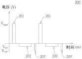
请参照图2A和图2B,图2A为根据本说明书的一实施例所绘示的非易失性存储器元件100的操作方法流程图。图2B为根据本说明书的另一实施例采用图2A的方法对非易失性存储器元件100进行写入操作200所绘示的操作时序图(timing diagram)。在本说明书的一些实施例中,非易失性存储器元件100的写入操作200方包括下述步骤:首先提供如图1所绘示的非易失性存储器元件100(如步骤S21所绘示)。Please refer to FIG. 2A and FIG. 2B . FIG. 2A is a flowchart illustrating an operation method of the
接着,对非易失性存储器元件100的至少一个可变电阻式存储单元101施加具有第一电性的写入脉冲201(如步骤S22所绘示)。例如,在本实施例中,写入脉冲201可以具有实质为1.6V的正向写入电压Vpgm;且具有实质介于500纳秒(nanosecond,ns)至3000纳秒之间的脉冲宽度。Next, a
然后,对可变电阻式存储单元101施加设定脉冲202(如步骤S23所绘示)。其中,设定脉冲202具有与第一电性相反的第二电性。例如,在本说明书的一些实施例中,设定脉冲202可以具有值实质介于-0.3V至-1.0V之间的设定电压Vset;具有实质介于1微秒(microsecond,μs)至3微秒之间的脉冲宽度。且设定脉冲202的设定电压Vset绝对值实质小于写入脉冲201的写入电压Vpgm绝对值(|Vset|<|Vpgm|)。在本实施例中,设定脉冲202可以具有实质为-0.5V的设定电压Vset,脉冲宽度优选约为1微秒。Then, the setting
后续,对可变电阻式存储单元101施加一个具有验证电压Vver的验证脉冲203(如步骤S24所绘示),以验证可变电阻式存储单元101的电阻值是否到达一个预设门限值(predetermined criteria)。在本说明书的一些实施例中,验证脉冲203的验证电压Vver绝对值实质大于或等于设定脉冲202的设定电压Vset绝对值(|Vset|≤|Vver|);且验证脉冲203的脉冲宽度远小于设定脉冲202的脉冲宽度。例如,在本实施例中,验证脉冲203可以具有正向的验证电压Vver。其中验证电压Vver实质为0.5V,验证电压Vver的脉冲宽度实质介于50纳秒(nanosecond,ns)至100纳秒之间,在一实施例中,优选为80纳秒。Subsequently, a
在验证过程中,当可变电阻式存储单元101的电阻值到达预设门限值(是)时,即结束写入操作200。当可变电阻式存储单元101的电阻值未能大于预设门限值(否)时,则回到步骤S22;再重复实施一次步骤S22、S23及S24。意即,对可变电阻式存储单元101再施加一次写入脉冲201(步骤S22)、设定脉冲202(步骤S23)和验证脉冲203(步骤S24),直到可变电阻式存储单元101的电阻值到达预设门限值。在本实施例之中,写入操作200在对可变电阻式存储单元101施加第一次的验证脉冲203之后,可变电阻式存储单元101的电阻值即已到达预设门限值,而结束写入操作200。因此,写入操作200总共仅对可变电阻式存储单元101施加一次写入脉201、一次设定脉冲202和一次验证脉冲203。In the verification process, when the resistance value of the variable
经过写入操作200之后,可变电阻式存储单元101的电阻值会大于预设电阻值,且经过一段时间之后,可变电阻式存储单元101的电阻分布状态不会再度恢复到先前较宽的电阻分布状态,而使部分可变电阻式存储单元101的电阻值小于此预设电阻值。进而可以解决写入操作不稳定的问题。After the
而值得注意的是,在本说明书的另一些实施例中,验证脉冲203以可以具有与写入脉冲201相反的电性。例如请参照图2C,图2C为根据本说明书的另一实施例采用图2A的方法对非易失性存储器元件进行写入操作200′所绘示的操作时序图。其中,图2C所绘示的操作时序图大致与图2B所绘示者相似,差别仅在于图2C的写入操作200′所采用的验证脉冲203′具有与写入脉冲201电性相反的负向电压。在本实施例中,验证脉冲203′的验证电压Vver′实质为-0.5V。虽然,验证脉冲203′和设定脉冲202都具有与写入脉冲201相反的电性,且二者的电压绝对值也都小于写入脉冲201的写入电压Vpgm绝对值。不过,由于验证脉冲203′的脉冲宽度远小于设定脉冲202的脉冲宽度。因此,仍可通过脉冲宽度和电压大小来区别验证脉冲203′和设定脉冲202。It is worth noting that, in other embodiments of the present specification, the verifying
请参照图3A和图3B,图3A为根据本说明书的一实施例所绘示的非易失性存储器元件100的操作方法流程图。图3B为绘示采用图3A所述的方法对非易失性存储器元件100进行写入操作300的操作时序图。在本说明书的一些实施例中,非易失性存储器元件100的写入操作300方包括下述步骤:首先提供如图1所绘示的非易失性存储器元件100(如步骤S31所绘示)。Please refer to FIG. 3A and FIG. 3B . FIG. 3A is a flowchart illustrating an operation method of the
接着,对非易失性存储器元件100的至少一个可变电阻式存储单元101施加具有第一电性的写入脉冲301(如步骤S32所绘示)。例如,在本实施例中,写入脉冲301可以具有实质为16V的正向写入电压Vpgm;以及实质介于500纳秒至3000纳秒之间的脉冲宽度。Next, a
然后,对可变电阻式存储单元101施加一个具有验证电压Vver的验证脉冲303(如步骤S33所绘示),以验证可变电阻式存储单元101的电阻值是否到达一个预设门限值。在本实施例中,验证脉冲303可以具有实质小于写入脉冲301的写入电压Vpgm的正向验证电压Vver(例如0.5V);且具有实质介于50纳秒至100纳秒之间的脉冲宽度。在一实施例中,验证脉冲303的脉冲宽度优选为80纳秒。Then, a
在验证过程中,当可变电阻式存储单元101的电阻值到达预设门限值(是)时,则进入步骤S34,对可变电阻式存储单元101施加设定脉冲302,然后结束写入操作300。相反的,当可变电阻式存储单元101的电阻值未能到达预设门限值(否)时,回到步骤S33,再次对可变电阻式存储单元101施加写入脉冲301(步骤S32)和验证脉冲303(步骤S33)。重复实施步骤S32和S33,直到可变电阻式存储单元101的电阻值到达预设门限值。之后,再对可变电阻式存储单元101施加设定脉冲302,随即结束写入操作300。其中,设定脉冲302具有与写入脉冲301电性相反的负向设定电压Vset;设定脉冲302的设定电压Vset绝对值实质小于或等于验证脉冲303的验证电压绝对值(|Vset|≤|Vver|);且验证脉冲303的脉冲宽度远小于设定脉冲302的脉冲宽度。In the verification process, when the resistance value of the variable
在本实施例之中,写入操作300在对可变电阻式存储单元101施加第一次的验证脉冲303之后,还重复实施了一次步骤S32和S33。因此,写入操作300总共对可变电阻式存储单元101施加二次写入脉冲301、二次设定脉冲302和一次设定脉冲302。经过写入操作300之后,可变电阻式存储单元101的电阻值会大于预设电阻值,且经过一段时间之后,可变电阻式存储单元101的电阻分布状态不会再度恢复到先前较宽的电阻分布状态,而使部分可变电阻式存储单元101的电阻值小于此预设电阻值。进而可以解决写入操作不稳定的问题。In this embodiment, after the
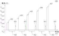
请参照图4A和图4B,图4A为根据本说明书的一实施例所绘示的非易失性存储器元件100的操作方法流程图。图4B为根据本说明书的另一实施例采用图4A的方法对非易失性存储器元件100进行写入操作400所绘示的操作时序图。在本说明书的一些实施例中,非易失性存储器元件100的写入操作400方包括下述步骤:首先提供如图1所绘示的非易失性存储器元件100(如步骤S41所绘示)。Please refer to FIG. 4A and FIG. 4B . FIG. 4A is a flowchart illustrating an operation method of the
接着,对非易失性存储器元件100的至少一个可变电阻式存储单元101施加具有第一电性的写入脉冲401(如步骤S42所绘示)。例如,在本实施例中,写入脉冲401可以具有实质为16V的正向写入电压Vpgm1;写入脉冲401的脉冲宽度实质介于500纳秒至3000纳秒之间。Next, a
然后,对可变电阻式存储单元101施加设定脉冲402(如步骤S43所绘示)。例如,在本说明书的一些实施例中,设定脉冲402可以具有值实质介于-0.3V至-1.0V之间的负向设定电压Vset,以及实质介于1微秒至3微秒之间的脉冲宽度。且设定脉冲402的设定电压Vset绝对值实质小于写入脉冲401的写入电压Vpgm1绝对值(|Vset|<|Vpgm1|)。在本实施例中,设定脉冲402可以具有实质0.5V的负向设定电压Vset,以及优选约为1微秒的脉冲宽度。Then, the setting
后续,对可变电阻式存储单元101施加一个具有验证电压Vver的验证脉冲403(如步骤S44所绘示),以验证可变电阻式存储单元101的电阻值是否到达一个预设门限值。当可变电阻式存储单元101的电阻值到达预设门限值(是)时,即结束写入操作400。在本说明书的实施例中,验证脉冲403的验证电压Vver的绝对值实质大于设定脉冲402的设定电压Vset的绝对值(|Vver|>|Vset|);且验证脉冲403的脉冲宽度远小于设定脉冲402的脉冲宽度。例如,在本实施例中,验证脉冲403是具有实质为0.5V的正向验证电压Vver,以及实质介于50纳秒至100纳秒之间的脉冲宽度。Subsequently, a
在步骤S44的验证过程中,若可变电阻式存储单元101的电阻值仍未到达此预设门限值(否),则进入步骤S45。对可变电阻式存储单元101施加具有第一电性的另一个写入脉冲(例如写入脉冲404)。在本实施例中,写入脉冲404的写入电压Vpgm2可以实质大于写入脉冲401的写入电压Vpgm1。之后,再实施一次步骤S43和步骤S44,对可变电阻式存储单元101施加设定脉冲402和验证脉冲403。重复步骤S45、S43和S44,直到可变电阻式存储单元101的电阻值到达预设门限值(是)时,再结束写入操作400。In the verification process of step S44, if the resistance value of the variable-
在本实施例之中,写入操作400在对可变电阻式存储单元101施加第一次的验证脉冲403之后,还重复实施了四次的步骤S45、步骤S43和步骤S44。因此,写入操作400总共对可变电阻式存储单元101施加四次写入脉冲404、405、406和407、五次设定脉冲402以及五次验证脉冲403(如图4B所绘示)。步骤S45所提供的写入脉冲404、405、406和407的写入电压Vpgm2、Vpgm3、Vpgm4和Vpgm5,实质大于写入脉冲401的写入电压Vpgm1。且写入电压值Vpgm1、Vpgm2、Vpgm3、Vpgm4和Vpgm5是逐次增加。In this embodiment, after the
而值得注意的是,当验证脉冲403′可以具有与设定脉冲402′相同电性时(即皆具有负向电性)时,验证脉冲403′和设定脉冲402′可以结合形成一个复合脉冲408。例如请参照图4C,图4C为根据本说明书的另一实施例采用图4A的方法对非易失性存储器元件进行写入操作400′所绘示的操作时序图。其中,图4C所绘示的写入操作400′的操作时序图大致与图4B所绘示的写入操作400的操作时序图相似,差别仅在于的写入操作400′所采用的验证脉冲403′具有实质为与写入脉冲401电性相反的负向验证电压Vver′,且负向验证电压Vver′实质低于设定脉冲402′的负向设定电压Vset。另外,验证脉冲403′和设定脉冲402′二者之间并无时间间隔,可以结合形成一个如图4C所绘示的锯齿状连续复合脉冲408。It is worth noting that when the verification pulse 403' can have the same electrical property as the setting pulse 402' (ie, both have negative electrical properties), the verification pulse 403' and the setting pulse 402' can be combined to form a composite pulse 408. For example, please refer to FIG. 4C . FIG. 4C is an operation timing diagram illustrating a
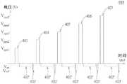
请参照图5A和图5B,图5A为根据本说明书的一实施例所绘示的非易失性存储器元件100的操作方法流程图。图5B为根据本说明书的一实施例采用图5A的方法对非易失性存储器元件100进行写入操作500所绘示的写入操作时序图。在本说明书的一些实施例中,非易失性存储器元件100的写入操作500方包括下述步骤:首先提供如图1所绘示的非易失性存储器元件100(如步骤S51所绘示)。Please refer to FIG. 5A and FIG. 5B . FIG. 5A is a flowchart illustrating an operation method of the
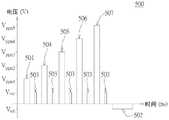
接着,对非易失性存储器元件100的至少一个可变电阻式存储单元101施加具有第一电性的写入脉冲501(如步骤S52所绘示)。例如,在本实施例中,写入脉冲501可以具有实质为16V的正向写入电压Vpgm1;写入脉冲501的脉冲宽度实质介于500纳秒至3000纳秒之间。Next, a
之后,对可变电阻式存储单元101施加一个具有验证电压Vver的验证脉冲503(如步骤S53所绘示),以验证可变电阻式存储单元101的电阻值是否到达一个预设门限值。在本实施例中,验证脉冲503可以具有实质小于写入脉冲501的正向验证电压Vver(例如0.5V);且具有实质介于50纳秒至100纳秒之间的脉冲宽度。After that, a
在步骤S53的验证过程,当可变电阻式存储单元101的电阻值到达预设门限值(是)时,写入操作500进入步骤S54:对可变电阻式存储单元101施加设定脉冲502,之后即结束写入操作500。在本实施例中,设定脉冲502可以具有实质为-0.5V的负向设定电压Vset,脉冲宽度约为1微秒。In the verification process of step S53 , when the resistance value of the variable
相反的,当可变电阻式存储单元101的电阻值仍未到达此预设门限值(否)时,则写入操作500进入步骤S55:对可变电阻式存储单元101施加具有第一电性的另一个写入脉冲(例如,写入脉冲504)。在本说明书的一些实施例中,写入脉冲504的写入电压Vpgm2可以实质大于写入脉冲501的写入电压Vpgm1。之后,再对可变电阻式存储单元101施加一次验证脉冲503(步骤S53)。重复实施步骤S55和S53,直到可变电阻式存储单元101的电阻值到达预设门限值。当可变电阻式存储单元101的电阻值到达预设门限值时,对可变电阻式存储单元101施加设定脉冲502(步骤S54),即结束写入操作500。On the contrary, when the resistance value of the variable
在本实施例之中,写入操作500在对可变电阻式存储单元101施加第一次的验证脉冲503之后,还重复实施了四次的步骤S55、S53和S54。因此,写入操作500总共对可变电阻式存储单元101施加五次写入脉冲501、504、505、506和507五次验证脉冲503以及一次设定脉冲502(如图5B所绘示)。步骤S55所提供的写入脉冲504、505、506和507的写入电压Vpgm2、Vpgm3、Vpgm4和Vpgm5,实质大于写入脉冲501的写入电压Vpgm1。且写入电压值Vpgm1、Vpgm2、Vpgm3、Vpgm4和Vpgm5逐次增加。In the present embodiment, after the
请参照图6A和图6B,图6A为根据本说明书的一实施例所绘示的非易失性存储器元件100的操作方法流程图。图6B为根据本说明书的另一实施例采用图6A的方法对非易失性存储器元件100进行写入操作600所绘示的操作时序图。在本说明书的一些实施例中,非易失性存储器元件100的写入操作600方包括下述步骤:首先提供如图1所绘示的非易失性存储器元件100(如步骤S61所绘示)。接着,对非易失性存储器元件100的至少一个可变电阻式存储单元101进行一前段写入操作S60A。之后,对可变电阻式存储单元101施加一设定脉冲602(如步骤S65所绘示)。后续,再进行一后段写入操作S60B。Please refer to FIG. 6A and FIG. 6B . FIG. 6A is a flowchart illustrating an operation method of the
前段写入操作S60A包括下述步骤:先对可变电阻式存储单元101施加具有第一电性的写入脉冲601(如步骤S62所绘示)。之后,对可变电阻式存储单元101施加一个具有验证电压Vver的验证脉冲603(如步骤S63所绘示),以验证可变电阻式存储单元101的电阻值是否到达一个预设门限值。The previous writing operation S60A includes the following steps: firstly applying a
在本实施例中,写入脉冲601可以具有实质为16V的正向写入电压Vpgm1;写入脉冲601的脉冲宽度实质介于500纳秒至3000纳秒之间。验证脉冲603可以具有实质小于写入脉冲601的正向验证电压Vver(例如0.5V);且具有实质介于50纳秒至100纳秒之间的脉冲宽度。In this embodiment, the
若经步骤S63验证,可变电阻式存储单元101的电阻值仍未到达此预设门限值(否),则进入步骤S64。对可变电阻式存储单元101施加具有第一电性的另一个写入脉冲(例如写入脉冲604)。写入脉冲604的写入电压Vpgm2可以实质大于写入脉冲401的写入电压Vpgm1。之后,再实施一次步骤S63,对可变电阻式存储单元101施加验证脉冲603。重复步骤S64和S63,直到可变电阻式存储单元101的电阻值到达预设门限值(是)时,完成前段写入操作S60A。If it is verified in step S63 that the resistance value of the variable
在本实施例中,前段写入操作S60A重复了二次步骤S64和S63。因此,前段写入操作S60A总共对可变电阻式存储单元101施加三次写入脉冲601、604和605以及三次验证脉冲603(如图6B所绘示)。步骤S64所提供的写入脉冲604和605的写入电压Vpgm2和Vpgm3实质大于写入脉冲601的写入电压Vpgm1,且逐次增加。In this embodiment, the previous-stage write operation S60A repeats steps S64 and S63 twice. Therefore, the previous writing operation S60A applies three writing
然后,进入步骤S65,对可变电阻式存储单元101施加设定脉冲602对可变电阻式存储单元101施加设定脉冲602。其中,设定脉冲602具有与第一电性相反的第二电性。设定脉冲602的设定电压Vset绝对值实质小于或等于验证脉冲603的验证电压Vver绝对值(|Vset|≤|Vver|)。且设定脉冲602的脉冲宽度远大于验证脉冲603的脉冲宽度。在本实施例中,设定脉冲602具有值实质为-0.5V的负向设定电压Vset,以及约为1微秒的脉冲宽度。Then, proceeding to step S65 , the setting
后续,再进行后段写入操作S60B,然后结束写入操作600。在本实施例中,后段写入操作S60B包括对可变电阻式存储单元101施加二次写入脉冲606和607以及二次验证脉冲608(如图6B所绘示)。其中,写入脉冲606和607的写入电压与写入脉冲601和604的写入电压Vpgm2和Vpgm3实质相同;且验证脉冲608的验证电压与验证脉冲603的验证电压Vver实质相同。由于后段写入操作S60B的实施内容,实质上与前段写入操作S60A相同。故不在此赘述。Subsequently, the next-stage write operation S60B is performed again, and then the
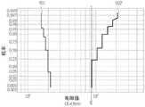
请参照图7A和图7B,图7A为绘示采用图5A所述的方法对非易失性存储器元件100进行如5B图所绘示的写入操作500并经过一段特定时间间隔后,可变电阻式存储单元101的电阻值累积分布函数图。图7B为绘示采用一比较例所提供的方法对非易失性存储器元件100进行写入操作并经过一段特定时间间隔后,可变电阻式存储单元101的电阻值累积分布函图。其中,本实施例所采用的写入操作500和比较例所采用的写入操作步骤程序与操作参数大致相同,差别仅在于比较例所采用的写入操方法省略了步骤S54,并未对可变电阻式存储单元101施加设定脉冲502。Please refer to FIG. 7A and FIG. 7B . FIG. 7A is a diagram illustrating that the
由图7A和图7B的结果可知,本实施例和比较例在进行写入操作之后,可变电阻式存储单元101的电阻值分布状态,可分别由第一电阻值分布状态(以电阻值累积分布函曲线701表示)偏移到第二电阻值分布状态(分别以电阻值累积分布函曲线702和702′表示),且可变电阻式存储单元101的电阻值会超过预设门限值K(例如87K-ohm)。经过一段特定时间间隔之后(例如,经过约为1秒时间间隔之后),大部分可变电阻式存储单元101的电阻值仍会维持超过预设门限值K的状态。但少部分可变电阻式存储单元101的电阻值会再度恢复到先前小于预设门限值K的状态。It can be seen from the results in FIGS. 7A and 7B that after the writing operation in the present embodiment and the comparative example, the distribution state of the resistance value of the variable
在本实施例中,采用图5A和图5B所述的方法进行写入操作500再经过一段特定时间间隔之后,可变电阻式存储单元101的电阻值低于预设门限值K的机率,实质小于百分之1(例如约为0.6%)(如图7A所绘示);而采用比较例的方法进行写入操作500′再经过一段特定时间间隔之后,可变电阻式存储单元101的电阻值低于预设门限值K的机率约为2%(如图7B所绘示)。显示采用图5A和图5B所述的方法来操作非易失性存储器元件100,可有效消除写入操作不稳定的现象,大幅增进非易失性存储器元件100的效能。In this embodiment, after a specific time interval has passed for the
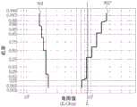
请参照图8A和图8B,图8A为绘示采用图6A所述的方法对非易失性存储器元件100进行如6B图所绘示的写入操作600,再经过一段特定时间间隔后,可变电阻式存储单元101的电阻值累积分布函数图。图8B为绘示采用一比较例所提供的方法对非易失性存储器元件100进行写入操作,再经过一段特定时间间隔后,可变电阻式存储单元101的电阻值累积分布函图。本实施例所采用的写入操作600和比较例所采用的写入操作步骤程序与操作参数大致相同,差别仅在于比较例所采用的写入操方法省略了步骤S65,并未对可变电阻式存储单元101施加设定脉冲602。Please refer to FIG. 8A and FIG. 8B . FIG. 8A is a diagram illustrating the
由图8A和图8B的结果可知,本实施例和比较例在进行写入操作之后,可变电阻式存储单元101的电阻值分布状态,可分别由第一电阻值分布状态(以电阻值累积分布函曲线801表示)偏移到第二电阻值分布状态(分别以电阻值累积分布函曲线802和802′表示),且可变电阻式存储单元101的电阻值会超过预设门限值K(例如87K-ohm)。再经过一段特定时间间隔之后(例如,经过约为1秒时间间隔之后),大部分可变电阻式存储单元101的电阻值仍会维持超过预设门限值K的状态。但少部分可变电阻式存储单元101的电阻值会再度恢复到先前小于预设门限值K的状态。8A and 8B, it can be seen that after the writing operation is performed in the present embodiment and the comparative example, the resistance value distribution state of the variable
在本实施例中,采用图6A和图6B所述的方法进行写入操作600,再经过一段特定时间间隔之后,全部的可变电阻式存储单元101中电阻值仍低于预设门限值K(如图8A所绘示);而采用比较例的方法进行写入操作,再经过一段特定时间间隔之后,可变电阻式存储单元101的电阻值低于预设门限值K的机率约为2%(如图8B所绘示)。显示采用图6A和图6B所述的方法来操作非易失性存储器元件100,可有效消除写入操作不稳定的现象,大幅增进非易失性存储器元件100的效能。In this embodiment, the method described in FIGS. 6A and 6B is used to perform the
另外值得注意的是,在本说明书的前述实施例中,设定脉冲的设定电压Vset大小是消除写入操作不稳定现象的重要因素之一。例如请参照图9A至图9D,图9A至图9D为采用图5A和图5B所述的方法,分别以-0.3V、-0.5V、-0.7V和-1.0V的设定电压Vset对非易失性存储器元件100进行写入操作500,再经过一段特定时间间隔后,可变电阻式存储单元101的电阻值累积分布图。It is also worth noting that, in the aforementioned embodiments of the present specification, the magnitude of the set voltage Vset of the set pulse is one of the important factors to eliminate the unstable phenomenon of the writing operation. For example, please refer to FIG. 9A to FIG. 9D. FIG. 9A to FIG. 9D use the method described in FIG. 5A and FIG. 5B, respectively, with the set voltage Vset of -0.3V, -0.5V, -0.7V and -1.0V. The
由图9A至图9D可观察到,采用-0.3V、-0.5V、-0.7V和-1.0V的设定电压Vset对非易失性存储器元件100进行写入操作500之后,可变电阻式存储单元101的电阻值分布状态,可分别由第一电阻值分布状态(以电阻值累积分布函曲线901表示)偏移到第二电阻值分布状态(分别以电阻值累积分布函曲线902、902′、902″和902″′表示),且可变电阻式存储单元101的电阻值会超过预设门限值K(例如87K-ohm)。再经过一段特定时间间隔之后,可变电阻式存储单元101的电阻值低于预设门限值K的机率,分别为0.7%、0、1%和2%。显示采用-0.5V的设定电压Vset来对非易失性存储器元件100进行写入操作500,藉以消除写入操作不稳定现象的效果(如图9B所绘示),优于采用-0.3V的设定电压Vset来对非易失性存储器元件100进行写入操作500来消除写入操作不稳定现象的效果(如图9A所绘示)。更优于采用-0.7V和-1.0V的设定电压Vset对非易失性存储器元件100进行写入操作500来消除写入操作不稳定现象的效果(如图9C和图9D所绘示)。It can be observed from FIGS. 9A to 9D that, after the
根据上述,本说明书的实施例是提供一种非易失性存储器元件的操作方法及其应用装置,其是在非易失性存储器元件的写入操作期间,对非易失性存储器元件的至少一个可变电阻式存储单元施加至少一个写入脉冲和一个验证脉冲。并在验证脉冲之前或之后,对此可变电阻式存储单元施加至少一个设定脉冲。其中设定脉冲具有一个与写入脉冲电性相反的设定电压,且设定电压绝对值实质小于或等于验证脉冲的验证电压绝的对值。可变电阻式存储单元在写入操作之后电阻值会大于一个预设电阻值。且经过一段时间之后,电阻分布状态不会再度恢复到先前较宽的电阻分布状态,而使部分小于此预设电阻值。进而可以解决可变电阻式存储单元写入操作不稳定的问题。Based on the above, the embodiments of the present specification provide a method of operating a nonvolatile memory element and an application device thereof, which perform at least an operation on the nonvolatile memory element during a write operation of the nonvolatile memory element. A variable resistance memory cell applies at least one write pulse and one verify pulse. And before or after the verification pulse, at least one setting pulse is applied to the variable resistance memory cell. The setting pulse has a setting voltage that is electrically opposite to the writing pulse, and the absolute value of the setting voltage is substantially less than or equal to the absolute value of the verification voltage of the verification pulse. The resistance value of the variable resistance memory cell after the writing operation is greater than a predetermined resistance value. And after a period of time, the resistance distribution state will not be restored to the previous wider resistance distribution state, and the part will be smaller than the preset resistance value. Further, the problem of unstable writing operation of the variable resistance memory cell can be solved.
虽然本说明书已以优选实施例揭露如上,然其并非用以限定本发明,任何该技术领域中普通技术人员,在不脱离本发明的精神和范围内,当可作部分的更改与修饰,因此本发明的保护范围当视权利要求所界定者为准。Although the present specification has disclosed the above with preferred embodiments, it is not intended to limit the present invention. Any person of ordinary skill in the technical field may make some changes and modifications without departing from the spirit and scope of the present invention. Therefore, The protection scope of the present invention shall be determined by the claims defined.
Claims (11)
Applications Claiming Priority (3)
| Application Number | Priority Date | Filing Date | Title |
|---|---|---|---|
| US201662416281P | 2016-11-02 | 2016-11-02 | |
| US15/649,672 | 2017-03-27 | ||
| US15/649,672US10401806B2 (en) | 2016-11-02 | 2017-07-14 | Adaptive control systems for buildings |
Publications (2)
| Publication Number | Publication Date |
|---|---|
| CN108665933A CN108665933A (en) | 2018-10-16 |
| CN108665933Btrue CN108665933B (en) | 2020-10-16 |
Family
ID=62021253
Family Applications (1)
| Application Number | Title | Priority Date | Filing Date |
|---|---|---|---|
| CN201710368406.9AActiveCN108665933B (en) | 2016-11-02 | 2017-05-22 | Operating method of non-volatile memory element and its application |
Country Status (2)
| Country | Link |
|---|---|
| US (3) | US10401806B2 (en) |
| CN (1) | CN108665933B (en) |
Families Citing this family (20)
| Publication number | Priority date | Publication date | Assignee | Title |
|---|---|---|---|---|
| US8600556B2 (en) | 2009-06-22 | 2013-12-03 | Johnson Controls Technology Company | Smart building manager |
| US10496048B2 (en)* | 2016-11-02 | 2019-12-03 | Edison Labs, Inc. | Switch terminal methods with wiring components secured to circuitry wiring without external live points of contact |
| US10394194B2 (en)* | 2016-11-02 | 2019-08-27 | Edison Labs, Inc. | Adaptive control methods for buildings with security |
| US10496047B2 (en)* | 2016-11-02 | 2019-12-03 | Edison Labs, Inc. | Adaptive control systems methods for buildings with security |
| US10067484B2 (en)* | 2016-11-02 | 2018-09-04 | Edison Labs, Inc. | Adaptive control systems for buildings with redundant circuitry |
| US11025563B2 (en) | 2017-04-13 | 2021-06-01 | Johnson Controls Technology Company | Space-aware network switch |
| US10599115B2 (en) | 2017-04-13 | 2020-03-24 | Johnson Controls Technology Company | Unified building management system with space use case profiles |
| US10742441B2 (en) | 2017-04-13 | 2020-08-11 | Johnson Controls Technology Company | Unified building management system |
| CN113485133A (en) | 2017-04-13 | 2021-10-08 | 江森自控科技公司 | Building management system with spatial profiles |
| US10852023B2 (en)* | 2018-05-15 | 2020-12-01 | Johnson Controls Technology Company | Building management autonomous HVAC control using reinforcement learning with occupant feedback |
| US10845081B2 (en)* | 2018-05-16 | 2020-11-24 | Johnson Controls Technology Company | Building management HVAC control using user voice feedback |
| KR102669026B1 (en)* | 2018-10-26 | 2024-05-27 | 삼성전자주식회사 | Electronic device and Method for controlling the electronic device thereof |
| KR102809926B1 (en)* | 2019-04-11 | 2025-05-22 | 삼성전자주식회사 | Home applicance and control method for the same |
| EP3767402B1 (en)* | 2019-07-19 | 2023-08-23 | Siemens Schweiz AG | System for heating, ventilation, air-conditioning |
| US10917740B1 (en) | 2019-07-30 | 2021-02-09 | Johnson Controls Technology Company | Laboratory utilization monitoring and analytics |
| US11151229B1 (en) | 2020-04-10 | 2021-10-19 | Avila Technology, LLC | Secure messaging service with digital rights management using blockchain technology |
| US10873852B1 (en) | 2020-04-10 | 2020-12-22 | Avila Technology, LLC | POOFster: a secure mobile text message and object sharing application, system, and method for same |
| US11536476B2 (en) | 2020-05-12 | 2022-12-27 | Johnson Controls Tyco IP Holdings LLP | Building system with flexible facility operation |
| US20210407690A1 (en) | 2020-06-25 | 2021-12-30 | Johnson Controls Technology Company | Systems and methods for a trusted consumer service |
| US11553618B2 (en)* | 2020-08-26 | 2023-01-10 | PassiveLogic, Inc. | Methods and systems of building automation state load and user preference via network systems activity |
Citations (3)
| Publication number | Priority date | Publication date | Assignee | Title |
|---|---|---|---|---|
| US20130094276A1 (en)* | 2011-10-18 | 2013-04-18 | Micron Technology, Inc. | Apparatuses and methods for determining stability of a memory cell |
| CN103594114A (en)* | 2012-08-15 | 2014-02-19 | 索尼公司 | Storage unit and driving method |
| CN104412326A (en)* | 2011-10-18 | 2015-03-11 | 美光科技公司 | Stabilization of resistive memory |
Family Cites Families (28)
| Publication number | Priority date | Publication date | Assignee | Title |
|---|---|---|---|---|
| KR0128169B1 (en) | 1993-12-31 | 1998-04-15 | 김광호 | Home automation system with user defined control |
| US6137869A (en) | 1997-09-16 | 2000-10-24 | Bell Atlantic Network Services, Inc. | Network session management |
| WO1999021977A1 (en)* | 1997-10-24 | 1999-05-06 | Life Technologies, Inc. | Recombinational cloning using nucleic acids having recombination sites |
| US20010010032A1 (en) | 1998-10-27 | 2001-07-26 | Ehlers Gregory A. | Energy management and building automation system |
| JP2005522164A (en) | 2002-03-28 | 2005-07-21 | ロバートショー コントロールズ カンパニー | Energy management system and method |
| US20050090915A1 (en)* | 2002-10-22 | 2005-04-28 | Smart Systems Technologies, Inc. | Programmable and expandable building automation and control system |
| US8214061B2 (en) | 2006-05-26 | 2012-07-03 | Abl Ip Holding Llc | Distributed intelligence automated lighting systems and methods |
| US8035320B2 (en) | 2007-04-20 | 2011-10-11 | Sibert W Olin | Illumination control network |
| US8086352B1 (en) | 2007-10-04 | 2011-12-27 | Scott Elliott | Predictive efficient residential energy controls |
| US8368321B2 (en) | 2008-04-14 | 2013-02-05 | Digital Lumens Incorporated | Power management unit with rules-based power consumption management |
| US8610376B2 (en) | 2008-04-14 | 2013-12-17 | Digital Lumens Incorporated | LED lighting methods, apparatus, and systems including historic sensor data logging |
| US10539311B2 (en) | 2008-04-14 | 2020-01-21 | Digital Lumens Incorporated | Sensor-based lighting methods, apparatus, and systems |
| GB0816721D0 (en) | 2008-09-13 | 2008-10-22 | Daniel Simon R | Systems,devices and methods for electricity provision,usage monitoring,analysis and enabling improvements in efficiency |
| US8487634B2 (en)* | 2008-09-25 | 2013-07-16 | Enmetric Systems, Inc. | Smart electrical wire-devices and premises power management system |
| WO2012065078A2 (en) | 2010-11-11 | 2012-05-18 | Rutgers, The State University Of New Jersey | System and method to measure and control power consumption in a residential or commercial building via a wall socket to ensure optimum energy usage therein |
| WO2015134789A1 (en) | 2014-03-05 | 2015-09-11 | View, Inc. | Monitoring sites containing switchable optical devices and controllers |
| WO2012123844A1 (en) | 2011-03-17 | 2012-09-20 | Koninklijke Philips Electronics N.V. | Reliable profiling for monitoring systems |
| US20130173926A1 (en) | 2011-08-03 | 2013-07-04 | Olea Systems, Inc. | Method, Apparatus and Applications for Biometric Identification, Authentication, Man-to-Machine Communications and Sensor Data Processing |
| US9448651B2 (en)* | 2012-01-09 | 2016-09-20 | Google Inc. | Intelligent touchscreen keyboard with finger differentiation |
| US20130201316A1 (en)* | 2012-01-09 | 2013-08-08 | May Patents Ltd. | System and method for server based control |
| US20140310075A1 (en)* | 2013-04-15 | 2014-10-16 | Flextronics Ap, Llc | Automatic Payment of Fees Based on Vehicle Location and User Detection |
| US9378601B2 (en)* | 2012-03-14 | 2016-06-28 | Autoconnect Holdings Llc | Providing home automation information via communication with a vehicle |
| US9529345B2 (en)* | 2013-12-05 | 2016-12-27 | Smartlabs, Inc. | Systems and methods to automatically adjust window coverings |
| US20150168002A1 (en) | 2013-12-18 | 2015-06-18 | Google Inc. | Systems and methods for determining or modifying a temperature program based on occupant activity |
| US20170084143A1 (en) | 2014-01-27 | 2017-03-23 | Nortek Security & Control Llc | Building security and automation system |
| US9578443B2 (en) | 2014-12-19 | 2017-02-21 | Smartlabs, Inc. | Smart home device adaptive configuration systems and methods |
| EP3332612B1 (en)* | 2015-08-05 | 2019-12-11 | Lutron Technology Company LLC | Load control system responsive to the location of an occupant and/or mobile device |
| US10119712B2 (en)* | 2015-10-21 | 2018-11-06 | Setra Systems | Room condition monitoring system |
- 2017
- 2017-05-22CNCN201710368406.9Apatent/CN108665933B/enactiveActive
- 2017-07-14USUS15/649,672patent/US10401806B2/ennot_activeExpired - Fee Related
- 2017-07-14USUS15/649,683patent/US10429801B2/ennot_activeExpired - Fee Related
- 2017-07-14USUS15/649,669patent/US10268168B2/ennot_activeExpired - Fee Related
Patent Citations (3)
| Publication number | Priority date | Publication date | Assignee | Title |
|---|---|---|---|---|
| US20130094276A1 (en)* | 2011-10-18 | 2013-04-18 | Micron Technology, Inc. | Apparatuses and methods for determining stability of a memory cell |
| CN104412326A (en)* | 2011-10-18 | 2015-03-11 | 美光科技公司 | Stabilization of resistive memory |
| CN103594114A (en)* | 2012-08-15 | 2014-02-19 | 索尼公司 | Storage unit and driving method |
Also Published As
| Publication number | Publication date |
|---|---|
| US10401806B2 (en) | 2019-09-03 |
| US20180120776A1 (en) | 2018-05-03 |
| US20180120801A1 (en) | 2018-05-03 |
| US20180120788A1 (en) | 2018-05-03 |
| US10429801B2 (en) | 2019-10-01 |
| CN108665933A (en) | 2018-10-16 |
| US10268168B2 (en) | 2019-04-23 |
Similar Documents
| Publication | Publication Date | Title |
|---|---|---|
| CN108665933B (en) | Operating method of non-volatile memory element and its application | |
| JP4838399B2 (en) | Nonvolatile memory device and method of writing to nonvolatile memory device | |
| US9378817B2 (en) | Variable resistance nonvolatile memory element writing method and variable resistance nonvolatile memory device | |
| US7359236B2 (en) | Read, write and erase circuit for programmable memory devices | |
| US7960224B2 (en) | Operation method for multi-level switching of metal-oxide based RRAM | |
| CN102800360B (en) | Method of forming process for variable resistive element and non-volatile semiconductor memory device | |
| CN102067234B (en) | Writing method of variable resistance nonvolatile memory element and variable resistance nonvolatile memory device | |
| JP6391014B2 (en) | Variable resistance nonvolatile memory device | |
| KR101193395B1 (en) | Non volatile memory cell and semiconductor memory device | |
| JP2014225316A (en) | Resistance change type nonvolatile storage and writing method thereon | |
| JPWO2010070895A1 (en) | Nonvolatile storage device and writing method thereof | |
| US9224470B1 (en) | Memory circuit and method of programming memory circuit | |
| JPWO2013140754A1 (en) | Resistance change nonvolatile memory element writing method and resistance change nonvolatile memory device | |
| CN114944181B (en) | A phase change memory operation method, phase change memory and memory system | |
| CN106611615B (en) | Operation method of resistance type memory cell and resistance type memory | |
| Lu et al. | ReRAM device and circuit co-design challenges in nano-scale CMOS technology | |
| US9947403B1 (en) | Method for operating non-volatile memory device and applications thereof | |
| TWI642057B (en) | Method for operating non-volatile memory device and applications thereof | |
| US10355207B2 (en) | Method for forming a non-volatile memory cell, non-volatile memory cell formed according to said method and microelectronic device comprising such memory cells | |
| CN113853654B (en) | Memory device and control method thereof | |
| CN109658963B (en) | Operation method of resistive memory storage device | |
| US11972799B2 (en) | Filament forming method for resistive memory unit | |
| JP2004355713A (en) | Multi-valued memory circuit | |
| An et al. | A 1Mb RRAM Macro with Bipolar Forming for Improved Programming Yield and Cell-by-cell Write Verification Scheme | |
| Grossi | Emerging non volatile memories reliability |
Legal Events
| Date | Code | Title | Description |
|---|---|---|---|
| PB01 | Publication | ||
| PB01 | Publication | ||
| SE01 | Entry into force of request for substantive examination | ||
| SE01 | Entry into force of request for substantive examination | ||
| GR01 | Patent grant | ||
| GR01 | Patent grant |