CN108630722B - Memory cell and method of forming the same, memory array structure and method of forming the same - Google Patents
Memory cell and method of forming the same, memory array structure and method of forming the sameDownload PDFInfo
- Publication number
- CN108630722B CN108630722BCN201710176063.6ACN201710176063ACN108630722BCN 108630722 BCN108630722 BCN 108630722BCN 201710176063 ACN201710176063 ACN 201710176063ACN 108630722 BCN108630722 BCN 108630722B
- Authority
- CN
- China
- Prior art keywords
- region
- diode
- well region
- well
- forming
- Prior art date
- Legal status (The legal status is an assumption and is not a legal conclusion. Google has not performed a legal analysis and makes no representation as to the accuracy of the status listed.)
- Active
Links
- 238000000034methodMethods0.000titleclaimsabstractdescription106
- 239000000758substrateSubstances0.000claimsabstractdescription125
- 238000002955isolationMethods0.000claimsabstractdescription77
- 238000003860storageMethods0.000claimsabstractdescription28
- 229910052751metalInorganic materials0.000claimsdescription53
- 239000002184metalSubstances0.000claimsdescription53
- 239000000463materialSubstances0.000claimsdescription15
- XUIMIQQOPSSXEZ-UHFFFAOYSA-NSiliconChemical compound[Si]XUIMIQQOPSSXEZ-UHFFFAOYSA-N0.000claimsdescription6
- 229910052710siliconInorganic materials0.000claimsdescription6
- 239000010703siliconSubstances0.000claimsdescription6
- 229910052581Si3N4Inorganic materials0.000claimsdescription4
- VYPSYNLAJGMNEJ-UHFFFAOYSA-NSilicium dioxideChemical groupO=[Si]=OVYPSYNLAJGMNEJ-UHFFFAOYSA-N0.000claimsdescription4
- HQVNEWCFYHHQES-UHFFFAOYSA-Nsilicon nitrideChemical compoundN12[Si]34N5[Si]62N3[Si]51N64HQVNEWCFYHHQES-UHFFFAOYSA-N0.000claimsdescription4
- 229910052814silicon oxideInorganic materials0.000claimsdescription4
- 238000000206photolithographyMethods0.000abstractdescription21
- 239000010410layerSubstances0.000description79
- 238000010586diagramMethods0.000description10
- 229920002120photoresistant polymerPolymers0.000description8
- 239000004065semiconductorSubstances0.000description4
- 239000012790adhesive layerSubstances0.000description3
- 230000015572biosynthetic processEffects0.000description3
- 150000002500ionsChemical class0.000description3
- RYGMFSIKBFXOCR-UHFFFAOYSA-NCopperChemical compound[Cu]RYGMFSIKBFXOCR-UHFFFAOYSA-N0.000description2
- GWEVSGVZZGPLCZ-UHFFFAOYSA-NTitan oxideChemical compoundO=[Ti]=OGWEVSGVZZGPLCZ-UHFFFAOYSA-N0.000description2
- MCMNRKCIXSYSNV-UHFFFAOYSA-NZirconium dioxideChemical compoundO=[Zr]=OMCMNRKCIXSYSNV-UHFFFAOYSA-N0.000description2
- 229910052782aluminiumInorganic materials0.000description2
- XAGFODPZIPBFFR-UHFFFAOYSA-NaluminiumChemical compound[Al]XAGFODPZIPBFFR-UHFFFAOYSA-N0.000description2
- 229910052802copperInorganic materials0.000description2
- 239000010949copperSubstances0.000description2
- 238000009792diffusion processMethods0.000description2
- 229910052733galliumInorganic materials0.000description2
- 229910052738indiumInorganic materials0.000description2
- 239000012212insulatorSubstances0.000description2
- WFKWXMTUELFFGS-UHFFFAOYSA-NtungstenChemical compound[W]WFKWXMTUELFFGS-UHFFFAOYSA-N0.000description2
- 229910052721tungstenInorganic materials0.000description2
- 239000010937tungstenSubstances0.000description2
- JBRZTFJDHDCESZ-UHFFFAOYSA-NAsGaChemical compound[As]#[Ga]JBRZTFJDHDCESZ-UHFFFAOYSA-N0.000description1
- GYHNNYVSQQEPJS-UHFFFAOYSA-NGalliumChemical compound[Ga]GYHNNYVSQQEPJS-UHFFFAOYSA-N0.000description1
- 229910001218Gallium arsenideInorganic materials0.000description1
- 229910000577Silicon-germaniumInorganic materials0.000description1
- LEVVHYCKPQWKOP-UHFFFAOYSA-N[Si].[Ge]Chemical compound[Si].[Ge]LEVVHYCKPQWKOP-UHFFFAOYSA-N0.000description1
- PNEYBMLMFCGWSK-UHFFFAOYSA-Naluminium oxideInorganic materials[O-2].[O-2].[O-2].[Al+3].[Al+3]PNEYBMLMFCGWSK-UHFFFAOYSA-N0.000description1
- 238000004458analytical methodMethods0.000description1
- 229910052787antimonyInorganic materials0.000description1
- 229910052785arsenicInorganic materials0.000description1
- 230000009286beneficial effectEffects0.000description1
- 230000000903blocking effectEffects0.000description1
- 229910052796boronInorganic materials0.000description1
- 239000003990capacitorSubstances0.000description1
- 230000000694effectsEffects0.000description1
- 238000005516engineering processMethods0.000description1
- 238000005530etchingMethods0.000description1
- 229910052732germaniumInorganic materials0.000description1
- GNPVGFCGXDBREM-UHFFFAOYSA-Ngermanium atomChemical compound[Ge]GNPVGFCGXDBREM-UHFFFAOYSA-N0.000description1
- APFVFJFRJDLVQX-UHFFFAOYSA-Nindium atomChemical compound[In]APFVFJFRJDLVQX-UHFFFAOYSA-N0.000description1
- 238000001459lithographyMethods0.000description1
- 238000004519manufacturing processMethods0.000description1
- 238000012986modificationMethods0.000description1
- 230000004048modificationEffects0.000description1
- 229910052698phosphorusInorganic materials0.000description1
- 238000002360preparation methodMethods0.000description1
- HBMJWWWQQXIZIP-UHFFFAOYSA-Nsilicon carbideChemical compound[Si+]#[C-]HBMJWWWQQXIZIP-UHFFFAOYSA-N0.000description1
- 229910010271silicon carbideInorganic materials0.000description1
Images


Classifications
- H—ELECTRICITY
- H10—SEMICONDUCTOR DEVICES; ELECTRIC SOLID-STATE DEVICES NOT OTHERWISE PROVIDED FOR
- H10B—ELECTRONIC MEMORY DEVICES
- H10B63/00—Resistance change memory devices, e.g. resistive RAM [ReRAM] devices
- H10B63/20—Resistance change memory devices, e.g. resistive RAM [ReRAM] devices comprising selection components having two electrodes, e.g. diodes
- H10B63/22—Resistance change memory devices, e.g. resistive RAM [ReRAM] devices comprising selection components having two electrodes, e.g. diodes of the metal-insulator-metal type
- H—ELECTRICITY
- H01—ELECTRIC ELEMENTS
- H01L—SEMICONDUCTOR DEVICES NOT COVERED BY CLASS H10
- H01L21/00—Processes or apparatus adapted for the manufacture or treatment of semiconductor or solid state devices or of parts thereof
- H01L21/02—Manufacture or treatment of semiconductor devices or of parts thereof
- H01L21/04—Manufacture or treatment of semiconductor devices or of parts thereof the devices having potential barriers, e.g. a PN junction, depletion layer or carrier concentration layer
- H01L21/18—Manufacture or treatment of semiconductor devices or of parts thereof the devices having potential barriers, e.g. a PN junction, depletion layer or carrier concentration layer the devices having semiconductor bodies comprising elements of Group IV of the Periodic Table or AIIIBV compounds with or without impurities, e.g. doping materials
- H01L21/26—Bombardment with radiation
- H01L21/263—Bombardment with radiation with high-energy radiation
- H01L21/265—Bombardment with radiation with high-energy radiation producing ion implantation
- H—ELECTRICITY
- H01—ELECTRIC ELEMENTS
- H01L—SEMICONDUCTOR DEVICES NOT COVERED BY CLASS H10
- H01L21/00—Processes or apparatus adapted for the manufacture or treatment of semiconductor or solid state devices or of parts thereof
- H01L21/70—Manufacture or treatment of devices consisting of a plurality of solid state components formed in or on a common substrate or of parts thereof; Manufacture of integrated circuit devices or of parts thereof
- H01L21/71—Manufacture of specific parts of devices defined in group H01L21/70
- H01L21/76—Making of isolation regions between components
- H01L21/762—Dielectric regions, e.g. EPIC dielectric isolation, LOCOS; Trench refilling techniques, SOI technology, use of channel stoppers
- H01L21/76224—Dielectric regions, e.g. EPIC dielectric isolation, LOCOS; Trench refilling techniques, SOI technology, use of channel stoppers using trench refilling with dielectric materials
- H—ELECTRICITY
- H10—SEMICONDUCTOR DEVICES; ELECTRIC SOLID-STATE DEVICES NOT OTHERWISE PROVIDED FOR
- H10B—ELECTRONIC MEMORY DEVICES
- H10B63/00—Resistance change memory devices, e.g. resistive RAM [ReRAM] devices
- H10B63/20—Resistance change memory devices, e.g. resistive RAM [ReRAM] devices comprising selection components having two electrodes, e.g. diodes
- H—ELECTRICITY
- H10—SEMICONDUCTOR DEVICES; ELECTRIC SOLID-STATE DEVICES NOT OTHERWISE PROVIDED FOR
- H10B—ELECTRONIC MEMORY DEVICES
- H10B63/00—Resistance change memory devices, e.g. resistive RAM [ReRAM] devices
- H10B63/80—Arrangements comprising multiple bistable or multi-stable switching components of the same type on a plane parallel to the substrate, e.g. cross-point arrays
- H—ELECTRICITY
- H10—SEMICONDUCTOR DEVICES; ELECTRIC SOLID-STATE DEVICES NOT OTHERWISE PROVIDED FOR
- H10D—INORGANIC ELECTRIC SEMICONDUCTOR DEVICES
- H10D62/00—Semiconductor bodies, or regions thereof, of devices having potential barriers
- H10D62/10—Shapes, relative sizes or dispositions of the regions of the semiconductor bodies; Shapes of the semiconductor bodies
- H10D62/113—Isolations within a component, i.e. internal isolations
- H10D62/115—Dielectric isolations, e.g. air gaps
- H—ELECTRICITY
- H10—SEMICONDUCTOR DEVICES; ELECTRIC SOLID-STATE DEVICES NOT OTHERWISE PROVIDED FOR
- H10N—ELECTRIC SOLID-STATE DEVICES NOT OTHERWISE PROVIDED FOR
- H10N70/00—Solid-state devices having no potential barriers, and specially adapted for rectifying, amplifying, oscillating or switching
- H10N70/011—Manufacture or treatment of multistable switching devices
- H—ELECTRICITY
- H10—SEMICONDUCTOR DEVICES; ELECTRIC SOLID-STATE DEVICES NOT OTHERWISE PROVIDED FOR
- H10N—ELECTRIC SOLID-STATE DEVICES NOT OTHERWISE PROVIDED FOR
- H10N70/00—Solid-state devices having no potential barriers, and specially adapted for rectifying, amplifying, oscillating or switching
- H10N70/801—Constructional details of multistable switching devices
- H10N70/821—Device geometry
- H10N70/826—Device geometry adapted for essentially vertical current flow, e.g. sandwich or pillar type devices
Landscapes
- Engineering & Computer Science (AREA)
- Physics & Mathematics (AREA)
- Manufacturing & Machinery (AREA)
- Condensed Matter Physics & Semiconductors (AREA)
- General Physics & Mathematics (AREA)
- Computer Hardware Design (AREA)
- Microelectronics & Electronic Packaging (AREA)
- Power Engineering (AREA)
- High Energy & Nuclear Physics (AREA)
- Health & Medical Sciences (AREA)
- Toxicology (AREA)
- Semiconductor Memories (AREA)
Abstract
Translated fromChinese
Description
Translated fromChinese技术领域technical field
本发明涉及半导体制造技术领域,特别涉及一种存储单元及其形成方法、存储阵列结构及其形成方法。The present invention relates to the technical field of semiconductor manufacturing, and in particular, to a memory cell and a method for forming the same, a memory array structure and a method for forming the same.
背景技术Background technique
半导体存储器是各种电子设备系统不可缺少的组成部分,而非易失半导体存储器具有能在断电情况下仍然保存数据的特性,因而被广泛运用于各种移动、便携设备上,如手机、笔记本、掌上电脑等。阻变式非易失存储器(RRAM,Resistance Random Access Memory)具有制备工艺简单、读写速度快、存储密度高、非易失以及与传统硅集成电路工艺兼容性好等优势,因此在半导体存储器领域具有巨大的应用潜力。Semiconductor memory is an indispensable part of various electronic equipment systems, and non-volatile semiconductor memory has the characteristics of being able to save data even in the event of a power failure, so it is widely used in various mobile and portable devices, such as mobile phones and notebooks. , Pocket PC, etc. Resistive non-volatile memory (RRAM, Resistance Random Access Memory) has the advantages of simple preparation process, fast read and write speed, high storage density, non-volatile and good compatibility with traditional silicon integrated circuit technology, so it is widely used in the field of semiconductor memory. Has huge application potential.
RRAM是基于一些材料的电诱导阻变效应发展起来的非易失存储器。它以简单的MIM(金属-绝缘体-金属,Metal-Insulator-Metal)电容结构为功能器件,其中绝缘层材料具有电诱导阻变特性,其电阻会在特定外加信号下发生可逆变化。RRAM根据施加在绝缘体上的电压的不同,使绝缘体的电阻在高阻态和低阻态间发生相应变化,从而开启或阻断电流流动通道。具体地,电阻由高阻态(off-state)向低阻态(on-state)转变,此编程过程为编程(set)操作;电阻由低阻态向高阻态转变,此编程过程称为擦除(reset)操作。RRAM is a non-volatile memory developed based on the electrically induced resistive switching effect of some materials. It uses a simple MIM (metal-insulator-metal, Metal-Insulator-Metal) capacitor structure as a functional device, in which the insulating layer material has an electrically induced resistance change characteristic, and its resistance changes reversibly under a specific external signal. Depending on the voltage applied to the insulator, the RRAM changes the resistance of the insulator between a high-resistance state and a low-resistance state, thereby opening or blocking the current flow path. Specifically, the resistance changes from a high resistance state (off-state) to a low resistance state (on-state), and this programming process is a programming (set) operation; the resistance changes from a low resistance state to a high resistance state, and this programming process is called Erase (reset) operation.
在每个RRAM器件上集成两个具有整流特性的二极管(diode),可以构成2D1R存储阵列结构,将所述2D1R存储阵列结构应用于存储结构中时,可以使存储结构具有高工作电流以及低漏电流的优势。Two diodes with rectification characteristics are integrated on each RRAM device to form a 2D1R memory array structure. When the 2D1R memory array structure is applied to the memory structure, the memory structure can have high operating current and low leakage. current advantage.
然而,现有技术形成的存储结构的性能仍有待提高。However, the performance of the memory structures formed by the prior art still needs to be improved.
发明内容SUMMARY OF THE INVENTION
本发明解决的问题是提供一种存储单元及其形成方法、存储阵列结构及其形成方法,使得形成存储单元中二极管所需的阱区的光刻工艺窗口增加,减小形成的存储单元以及存储阵列结构的尺寸。The problem solved by the present invention is to provide a memory cell and its formation method, a memory array structure and its formation method, so that the photolithography process window of the well region required for forming the diode in the memory cell is increased, and the formed memory cell and the memory cell are reduced. The size of the array structure.
为解决上述问题,本发明提供一种存储单元,包括:基底,所述基底包括沿行方向依次排列的第一二极管区、第二二极管区、第三二极管区以及第四二极管区;位于所述第一二极管区以及第二二极管区的基底内的第一阱区;位于所述第三二极管区以及第四二极管区的基底内的第二阱区,且所述第二阱区的掺杂类型与所述第一阱区的掺杂类型不同;分别位于所述第一阱区以及第二阱区上的掺杂导电区;位于所述基底内的深沟槽隔离结构,其中,所述深沟槽隔离结构电隔离所述第一二极管区的第一阱区与所述第二二极管区的第一阱区,电隔离所述第三二极管区的第二阱区与所述第四二极管区的第二阱区,电隔离所述第一二极管区的掺杂导电区与所述第二二极管区的掺杂导电区,电隔离所述第三二极管区与所述第四二极管区的掺杂导电区;位于所述基底上方的RRAM器件,所述RRAM器件电连接所述第二二极管区的掺杂导电区以及第三二极管区的掺杂导电区。In order to solve the above problems, the present invention provides a memory cell, comprising: a substrate, the substrate includes a first diode region, a second diode region, a third diode region and a fourth diode region arranged in sequence along a row direction a diode region; a first well region located in the substrate of the first diode region and the second diode region; located in the substrate of the third diode region and the fourth diode region a second well region, and the doping type of the second well region is different from the doping type of the first well region; the doped conductive regions respectively located on the first well region and the second well region; located in a deep trench isolation structure in the substrate, wherein the deep trench isolation structure electrically isolates the first well region of the first diode region and the first well region of the second diode region, electrically isolating the second well region of the third diode region from the second well region of the fourth diode region, electrically isolating the doped conductive region of the first diode region and the second well region a doped conductive region of the diode region, electrically isolating the third diode region from the doped conductive region of the fourth diode region; an RRAM device located above the substrate, the RRAM device being electrically connected The doped conductive region of the second diode region and the doped conductive region of the third diode region.
可选的,所述存储单元还包括:导电插塞,所述导电插塞分别位于所述第二二极管区以及第三二极管区的掺杂导电区上;电连接所述导电插塞的金属层,且所述金属层位于所述导电插塞与所述RRAM器件之间。Optionally, the storage unit further includes: conductive plugs, the conductive plugs are respectively located on the doped conductive regions of the second diode region and the third diode region; electrically connected to the conductive plugs A metal layer of the plug, and the metal layer is located between the conductive plug and the RRAM device.
可选的,所述深沟槽隔离结构还电隔离所述第二二极管区的第一阱区与所述第三二极管区的第二阱区,且还电隔离所述第二二极管区的掺杂导电区与所述第三二极管区的掺杂导电区。Optionally, the deep trench isolation structure further electrically isolates the first well region of the second diode region and the second well region of the third diode region, and also electrically isolates the second well region. The doped conductive region of the diode region and the doped conductive region of the third diode region.
可选的,所述深沟槽隔离结构的材料为氧化硅、氮化硅或氮氧化硅。Optionally, the material of the deep trench isolation structure is silicon oxide, silicon nitride or silicon oxynitride.
可选的,所述存储单元还包括:位于基底内的N型深阱区,且所述N型深阱区位于所述第一阱区以及第二阱区下方,其中,所述深沟槽隔离结构底部低于所述N型深阱区底部。Optionally, the memory unit further includes: an N-type deep well region located in the substrate, and the N-type deep well region is located under the first well region and the second well region, wherein the deep trench is The bottom of the isolation structure is lower than the bottom of the N-type deep well region.
可选的,所述第一阱区的掺杂类型为N型或者P型;所述第二阱区的掺杂类型为N型或者P型;所述掺杂导电区的掺杂类型为N型或者P型。Optionally, the doping type of the first well region is N-type or P-type; the doping type of the second well region is N-type or P-type; the doping type of the doped conductive region is N type or P type.
可选的,所述第一阱区的掺杂类型与位于所述第一阱区上方的掺杂导电区的掺杂类型不同;所述第二阱区的掺杂类型与位于所述第二阱区上方的掺杂导电区的掺杂类型不同。Optionally, the doping type of the first well region is different from the doping type of the doped conductive region located above the first well region; the doping type of the second well region is different from the doping type of the doped conductive region located above the first well region; The doping types of the doped conductive regions above the well regions are different.
本发明还提供一种存储单元的形成方法,包括:提供基底,所述基底包括沿行方向依次排列的第一二极管区、第二二极管区、第三二极管区以及第四二极管区;在所述第一二极管区以及第二二极管区的基底内形成第一阱区;在所述第三二极管区以及第四二极管区的基底内形成第二阱区,且所述第二阱区的掺杂类型与所述第一阱区的掺杂类型不同;在所述第一阱区以及第二阱区上形成掺杂导电区;在所述基底内形成深沟槽隔离结构,且所述深沟槽隔离结构电隔离所述第一二极管区的第一阱区与所述第二二极管区的第一阱区,电隔离所述第三二极管区的第二阱区与所述第四二极管区的第二阱区,电隔离所述第一二极管区的掺杂导电区与所述第二二极管区的掺杂导电区,电隔离所述第三二极管区与所述第四二极管区的掺杂导电区;在所述基底上方形成RRAM器件,所述RRAM器件电连接所述第二二极管区的掺杂导电区以及第三二极管区的掺杂导电区。The present invention also provides a method for forming a memory cell, comprising: providing a substrate, the substrate including a first diode region, a second diode region, a third diode region and a fourth diode region sequentially arranged along a row direction a diode region; a first well region is formed in the substrate of the first diode region and the second diode region; formed in the substrate of the third diode region and the fourth diode region a second well region, and the doping type of the second well region is different from the doping type of the first well region; a doped conductive region is formed on the first well region and the second well region; A deep trench isolation structure is formed in the substrate, and the deep trench isolation structure electrically isolates the first well region of the first diode region and the first well region of the second diode region, and electrically isolates The second well region of the third diode region and the second well region of the fourth diode region electrically isolate the doped conductive region of the first diode region from the second diode A doped conductive region of the tube region electrically isolates the third diode region from the doped conductive region of the fourth diode region; an RRAM device is formed above the substrate, and the RRAM device is electrically connected to the The doped conductive region of the second diode region and the doped conductive region of the third diode region.
可选的,先形成所述第一阱区以及第二阱区,后形成所述深沟槽隔离结构;或者,先形成所述深沟槽隔离结构,后形成所述第一阱区以及第二阱区。Optionally, the first well region and the second well region are formed first, and then the deep trench isolation structure is formed; or, the deep trench isolation structure is formed first, and then the first well region and the first well region are formed. Two well region.
可选的,所述存储单元还包括:位于基底内的N型深阱区,且所述N型深阱区位于所述第一阱区以及第二阱区下方;在形成所述第一阱区以及第二阱区之前,还包括:在所述基底内形成N型深阱区。Optionally, the memory unit further includes: an N-type deep well region located in the substrate, and the N-type deep well region is located under the first well region and the second well region; after forming the first well region Before the second well region and the second well region, the method further includes: forming an N-type deep well region in the substrate.
可选的,在形成所述RRAM器件之前,还包括:分别在所述第二二极管区以及第三二极管区的掺杂导电区上形成导电插塞;形成电连接所述导电插塞的金属层,且所述金属层位于所述导电插塞与所述RRAM器件之间。Optionally, before forming the RRAM device, the method further includes: forming conductive plugs on the doped conductive regions of the second diode region and the third diode region respectively; forming electrically connecting the conductive plugs A metal layer of the plug, and the metal layer is located between the conductive plug and the RRAM device.
本发明还提供一种存储阵列结构,包括:若干个沿行方向和列方向分布的前述存储单元,所述行方向与列方向相互垂直,其中,处于同一列存储单元的第一二极管区的第一阱区相连通,处于同一列存储单元的第二二极管区的第一阱区相连通,处于同一列存储单元的第三二极管区的第二阱区相连通,处于同一列存储单元的第四二极管区的第二阱区相连通;字线,同一字线对应电连接处于同一行的存储单元的RRAM器件;复位线,同一复位线对应电连接处于同一列存储单元的第一二极管区或者第二二极管区的第一阱区;位线,同一位线对应电连接处于同一列存储单元的第三二极管区或者第四二极管区的第二阱区。The present invention also provides a memory array structure, comprising: a plurality of the aforementioned memory cells distributed along a row direction and a column direction, wherein the row direction and the column direction are perpendicular to each other, wherein the first diode region of the memory cells in the same column The first well regions of the memory cells are connected to each other, the first well regions of the second diode regions of the memory cells in the same column are connected to each other, and the second well regions of the third diode regions of the memory cells of the same column are connected to each other. The second well regions of the fourth diode regions of the column memory cells are connected; word lines, the same word line is correspondingly electrically connected to the RRAM devices of the memory cells in the same row; reset lines, the same reset line is correspondingly electrically connected to the same column of memory cells The first diode region of the unit or the first well region of the second diode region; the bit line, the same bit line is correspondingly electrically connected to the third diode region or the fourth diode region of the same column of memory cells. the second well region.
可选的,所述存储阵列结构还包括:位于所述基底内与所述复位线电连接的复位线选通二极管,以及与所述位线电连接的位线选通二极管,且所述复位选通二极管以及位线选通二极管沿行方向分布;其中,所述复位线选通二极管包括:位于所述基底内的复位线选通阱区,与处于同一列的存储单元的第一阱区相连通;位于所述复位线选通阱区上的复位线掺杂导电区,且所述复位线掺杂导电区的掺杂类型与所述复位线选通阱区的掺杂类型相同,所述复位线掺杂导电区与所述复位线电连接;所述位线选通二极管包括:位于所述基底内的位线选通阱区,与处于同一列的存储单元的第二阱区相连通;位于所述位线选通阱区上的位线掺杂导电区,且所述位线掺杂导电区的掺杂类型与所述位线选通阱区的掺杂类型相同,所述位线掺杂导电区与所述位线电连接。Optionally, the memory array structure further includes: a reset line gate diode located in the substrate and electrically connected to the reset line, and a bit line gate diode electrically connected to the bit line, and the reset line The gate diodes and the bit line gate diodes are distributed along the row direction; wherein, the reset line gate diodes include: a reset line gate well region located in the substrate, and a first well region of the memory cells in the same column The reset line doped conductive region located on the reset line gate well region, and the doping type of the reset line doped conductive region is the same as the doping type of the reset line gate well region, so The reset line doped conductive region is electrically connected to the reset line; the bit line gate diode includes: a bit line gate well region located in the substrate and connected to the second well region of the memory cells in the same column The bit line doped conductive region located on the bit line gate well region, and the doping type of the bit line doped conductive region is the same as the doping type of the bit line gate well region, the A bit line doped conductive region is electrically connected to the bit line.
可选的,所述存储单元还包括:所述导电插塞,所述导电插塞分别位于所述第二二极管区以及第三二极管区的掺杂导电区上;电连接所述导电插塞的金属层,其中,所述RRAM器件位于所述金属层上;其中,所述复位线与所述金属层处于同层,且所述位线与所述金属层处于同层。Optionally, the storage unit further includes: the conductive plugs, the conductive plugs are respectively located on the doped conductive regions of the second diode region and the third diode region; electrically connected to the A metal layer of a conductive plug, wherein the RRAM device is located on the metal layer; wherein, the reset line is in the same layer as the metal layer, and the bit line is in the same layer as the metal layer.
可选的,相邻列的存储单元通过所述深沟槽隔离结构电隔离;所述存储阵列结构还包括:位于所述基底内的浅沟槽隔离结构,所述浅沟槽隔离结构电隔离相邻行的存储单元的掺杂导电区。Optionally, memory cells in adjacent columns are electrically isolated by the deep trench isolation structure; the memory array structure further includes: a shallow trench isolation structure located in the substrate, and the shallow trench isolation structure is electrically isolated Doped conductive regions of adjacent rows of memory cells.
本发明还提供一种存储阵列结构的形成方法,包括:形成若干个沿行方向和列方向分布的存储单元,其中,处于同一列存储单元的第一二极管区的第一阱区相连通,处于同一列存储单元的第二二极管区的第一阱区相连通,处于同一列存储单元的第三二极管区的第二阱区相连通,处于同一列存储单元的第四二极管区的第二阱区相连通;其中,形成所述存储单元的步骤包括:提供基底,所述基底包括沿行方向依次排列的第一二极管区、第二二极管区、第三二极管区以及第四二极管区;在所述第一二极管区以及第二二极管区的基底内形成第一阱区;在所述第三二极管区以及第四二极管区的基底内形成第二阱区,且所述第二阱区的掺杂类型与所述第一阱区的掺杂类型不同;在所述第一阱区以及第二阱区上形成掺杂导电区;在所述基底内形成深沟槽隔离结构,且所述深沟槽隔离结构电隔离所述第一二极管区的第一阱区与所述第二二极管区的第一阱区,电隔离所述第三二极管区的第二阱区与所述第四二极管区的第二阱区,电隔离所述第一二极管区的掺杂导电区与所述第二二极管区的掺杂导电区,电隔离所述第三二极管区与所述第四二极管区的掺杂导电区;形成RRAM器件,所述RRAM器件电连接所述第二二极管区的掺杂导电区以及第三二极管区的掺杂导电区;形成字线,且同一字线对应电连接处于同一行的存储单元的RRAM器件;形成复位线,同一复位线对应电连接处于同一列存储单元的第一二极管区或者第二二极管区的第一阱区;形成位线,同一位线对应电连接处于同一列存储单元的第三二极管区或者第四二极管区的第二阱区。The present invention also provides a method for forming a memory array structure, comprising: forming a plurality of memory cells distributed along the row direction and the column direction, wherein the first well regions of the first diode regions of the memory cells in the same column are connected to each other. , the first well region of the second diode region in the same column of memory cells is connected, the second well region of the third diode region of the same column of memory cells is connected, the fourth and second well regions of the same column of memory cells are connected The second well region of the electrode tube region is connected to each other; wherein, the step of forming the storage unit includes: providing a substrate, and the substrate includes a first diode region, a second diode region, a first diode region, a second diode region, and a Three diode regions and a fourth diode region; a first well region is formed in the substrate of the first diode region and the second diode region; the third diode region and the fourth diode region are formed A second well region is formed in the substrate of the diode region, and the doping type of the second well region is different from the doping type of the first well region; on the first well region and the second well region forming a doped conductive region; forming a deep trench isolation structure in the substrate, and the deep trench isolation structure electrically isolates the first well region of the first diode region and the second diode region the first well region, electrically isolating the second well region of the third diode region and the second well region of the fourth diode region, electrically isolating the doped conductive region of the first diode region The doped conductive region of the second diode region and the second diode region are electrically isolated from the doped conductive region of the third diode region and the fourth diode region; an RRAM device is formed, and the RRAM device is electrically connecting the doped conductive region of the second diode region and the doped conductive region of the third diode region; forming a word line, and the same word line is correspondingly electrically connected to the RRAM devices of the memory cells in the same row; forming a reset The same reset line is correspondingly electrically connected to the first diode region or the first well region of the second diode region in the same column of memory cells; a bit line is formed, and the same bit line is correspondingly electrically connected to the first well region of the same column of memory cells. The third diode region or the second well region of the fourth diode region.
可选的,先形成所述第一阱区以及第二阱区,后形成所述深沟槽隔离结构;或者,先形成所述深沟槽隔离结构,后形成所述第一阱区以及第二阱区。Optionally, the first well region and the second well region are formed first, and then the deep trench isolation structure is formed; or, the deep trench isolation structure is formed first, and then the first well region and the first well region are formed. Two well region.
可选的,在所述基底内形成浅沟槽隔离结构,所述浅沟槽隔离结构电隔离相邻行的存储单元的掺杂导电区。Optionally, a shallow trench isolation structure is formed in the substrate, and the shallow trench isolation structure electrically isolates doped conductive regions of memory cells in adjacent rows.
可选的,所述形成方法还包括:在所述基底内形成与所述复位线电连接的复位线选通二极管,形成与所述位线电连接的位线选通二极管,且所述复位线选通二极管以及位线选通二极管沿行向分布;形成所述复位线选通二极管的工艺步骤包括:在形成所述第一阱区的工艺步骤中,在所述基底内形成复位线选通阱区,且所述复位线选通阱区与处于同一列的存储单元的第一阱区相连通;在形成所述掺杂导电区的工艺步骤中,在所述复位线选通阱区上形成复位线掺杂导电区,且所述复位线掺杂导电区的掺杂类型与所述复位线选通阱区的掺杂类型相同,所述复位线掺杂导电区与所述复位线电连接;形成所述位线选通二极管的工艺步骤包括:在形成所述第二阱区的工艺步骤中,在所述基底内形成位线选通阱区,且所述位线选通阱区与处于同一列的存储单元的第二阱区相连通;在形成所述掺杂导电区的工艺步骤中,在所述位线选通阱区上形成位线掺杂导电区,且所述位线掺杂导电区的掺杂类型与所述位线选通阱区的掺杂类型相同,所述位线掺杂导电区与所述位线电连接。Optionally, the forming method further includes: forming a reset line gate diode electrically connected to the reset line in the substrate, forming a bit line gate diode electrically connected to the bit line, and the reset line Line gate diodes and bit line gate diodes are distributed along the row direction; the process step of forming the reset line gate diode includes: in the process step of forming the first well region, forming a reset line gate diode in the substrate well region, and the reset line gate well region is connected with the first well region of the memory cells in the same column; in the process step of forming the doped conductive region, the reset line gate well region is A reset line doped conductive region is formed thereon, and the doping type of the reset line doped conductive region is the same as that of the reset line gate well region, and the reset line doped conductive region is the same as that of the reset line. Electrical connection; the process step of forming the bit line gate diode includes: in the process step of forming the second well region, forming a bit line gate well region in the substrate, and the bit line gate well region In the process step of forming the doped conductive region, a bit line doped conductive region is formed on the bit line gate well region, and the The doping type of the bit line doped conductive region is the same as that of the bit line gate well region, and the bit line doped conductive region is electrically connected to the bit line.
可选的,在形成所述RRAM器件之前,还包括:分别在所述第二二极管区以及第三二极管区的掺杂导电区上形成导电插塞;形成电连接所述导电插塞的金属层,且所述金属层位于所述导电插塞与所述RRAM器件之间;在形成所述金属层的工艺步骤中,还形成所述复位线以及位线。Optionally, before forming the RRAM device, the method further includes: forming conductive plugs on the doped conductive regions of the second diode region and the third diode region respectively; forming electrically connecting the conductive plugs The metal layer of the plug, and the metal layer is located between the conductive plug and the RRAM device; in the process step of forming the metal layer, the reset line and the bit line are also formed.
与现有技术相比,本发明的技术方案具有以下优点:Compared with the prior art, the technical solution of the present invention has the following advantages:
本发明提供的存储单元的形成方法的技术方案中,在第一二极管区以及第二二极管区的基底内形成第一阱区,在第三二极管区以及第四二极管区的基底内形成第二阱区,使得形成所述第一阱区的光刻工艺窗口较在单个二极管区的基底内形成第一阱区的光刻工艺窗口大,且形成所述第二阱区的光刻工艺窗口较在单个二极管区的基底内形成第二阱区的光刻工艺窗口大,因此本发明中形成第一阱区以及第二阱区的光刻工艺窗口均增加,从而可以改善形成的第一阱区以及第二阱区的位置精确度;此外,由于第一阱区以及第二阱区的光刻工艺窗口增加,相应使得形成的存储单元的面积可以做的更小。在第一阱区以及第二阱区上形成掺杂导电区,所述掺杂导电区与位于其下方的第一阱区构成二极管,所述掺杂导电区域位于其下方的第二阱区构成二极管;在基底内形成深沟槽隔离结构,用于电隔离第一二极管区和第二二极管区的第一阱区,且电隔离第三二极管区和第四二极管区的第二阱区,且电各类相邻二极管区的掺杂导电区,从而形成相互电绝缘的二极管;还形成电连接第二二极管区的掺杂导电区以及第三二极管区的掺杂导电区的RRAM器件,以构成2D1R结构。因此,本发明形成的存储单元中2D1R结构占据的面积小。In the technical solution of the method for forming a memory cell provided by the present invention, the first well region is formed in the substrate of the first diode region and the second diode region, and the third diode region and the fourth diode are formed in the substrate. A second well region is formed in the substrate of the single diode region, so that the photolithography process window for forming the first well region is larger than the photolithography process window for forming the first well region in the substrate of a single diode region, and the second well region is formed The photolithography process window of the diode region is larger than the photolithography process window for forming the second well region in the substrate of a single diode region. Therefore, in the present invention, the photolithography process windows for forming the first well region and the second well region are increased, so that the The positional accuracy of the formed first well region and the second well region is improved; in addition, since the photolithography process windows of the first well region and the second well region are increased, the area of the formed memory cell can be made smaller accordingly. A doped conductive region is formed on the first well region and the second well region, the doped conductive region and the first well region below the doped conductive region form a diode, and the doped conductive region below the second well region forms a diode A diode; a deep trench isolation structure is formed in a substrate for electrically isolating a first diode region and a first well region of the second diode region, and electrically isolating a third diode region and a fourth diode The second well region of the diode region, and the doped conductive regions of the various adjacent diode regions, thereby forming diodes that are electrically isolated from each other; also form the doped conductive regions that electrically connect the second diode region and the third diode The doped conductive region of the RRAM device to form a 2D1R structure. Therefore, the area occupied by the 2D1R structure in the memory cell formed by the present invention is small.
本发明提供的存储阵列结构的形成方法的技术方案中,包括上述提到的存储单元,因此,本发明形成的存储阵列结构面积也可以做的很小。The technical solution of the method for forming a memory array structure provided by the present invention includes the above-mentioned memory cells. Therefore, the area of the memory array structure formed by the present invention can also be made small.
附图说明Description of drawings
图1至图5为本发明实施例提供的存储单元形成方法各步骤对应的结构示意图;1 to 5 are schematic structural diagrams corresponding to each step of a method for forming a memory cell according to an embodiment of the present invention;
图6至图14为本发明实施例提供的存储阵列结构形成方法各步骤对应的结构示意图;6 to 14 are schematic structural diagrams corresponding to each step of a method for forming a memory array structure according to an embodiment of the present invention;
图15为本发明实施例提供的存储阵列结构等效电路图。FIG. 15 is an equivalent circuit diagram of a memory array structure provided by an embodiment of the present invention.
具体实施方式Detailed ways
由背景技术可知,现有技术形成的存储结构的性能有待提高。It can be known from the background art that the performance of the storage structure formed in the prior art needs to be improved.
经分析发现,随着器件朝向小型化微型化方向发展,形成存储结构中的二极管所需的阱区的光刻工艺窗口越来越小,使得形成的存储结构的性能有待提高。Through analysis, it is found that with the development of the device towards miniaturization, the photolithography process window of the well region required to form the diode in the memory structure is getting smaller and smaller, so that the performance of the formed memory structure needs to be improved.
为解决上述问题,本发明提供一种存储单元的形成方法,使得二极管中的阱区的光刻工艺窗口增加,从而改善形成的存储单元的性能。In order to solve the above problems, the present invention provides a method for forming a memory cell, so that the photolithography process window of the well region in the diode is increased, thereby improving the performance of the formed memory cell.
为使本发明的上述目的、特征和优点能够更为明显易懂,下面结合附图对本发明的具体实施例做详细的说明。In order to make the above objects, features and advantages of the present invention more clearly understood, the specific embodiments of the present invention will be described in detail below with reference to the accompanying drawings.
图1至图5为本发明一实施例提供的存储单元形成方法各步骤对应的结构示意图。1 to 5 are schematic structural diagrams corresponding to each step of a method for forming a memory cell according to an embodiment of the present invention.
参考图1及图2,图1为俯视结构示意图,图2为图1中沿AA1方向的剖面结构示意图,提供基底10,所述基底10包括沿行方向依次排列的第一二极管区1、第二二极管区2、第三二极管区3以及第四二极管区4。Referring to FIGS. 1 and 2 , FIG. 1 is a schematic top view of the structure, and FIG. 2 is a schematic cross-sectional structure of FIG. 1 along the AA1 direction, a
所述基底10为后续形成二极管提供工艺平台。The
本实施例中,所述基底10的材料为硅。在其他实施例中,所述基底的材料还可以为锗、锗化硅、碳化硅、砷化镓或者镓化铟。In this embodiment, the material of the
其中,后续在第一二极管区1以及第二二极管区2形成的二极管极性相同;后续在第三二极管区3以及第四二极管区4形成的二极管极性相同;并且,在所述第一二极管区1以及第三二极管区3形成的二极管极性相反。Wherein, the diodes subsequently formed in the
继续参考图1及图2,在所述第一二极管区1以及第二二极管区2的基底10内形成第一阱区11;在所述第三二极管区3以及第四二极管区4的基底内形成第二阱区12,且所述第二阱区12的掺杂类型与所述第一阱区11的掺杂类型不同。1 and 2, a
所述第一阱区11的的掺杂类型为N型或者P型;所述第二阱区12的掺杂类型为N型或者P型。其中,N型掺杂的掺杂离子为P、As或者Sb,P型掺杂的掺杂离子为B、Ga或者In。The doping type of the
本实施例中,以所述第一阱区11的掺杂类型为P型,所述第二阱区12 的掺杂类型为N型为例。In this embodiment, the doping type of the
形成所述第一阱区11的工艺步骤包括:在所述第三二极管区3以及第四二极管区4的基底10上形成第一光刻胶层;以所述第一光刻胶层为掩膜,对所述第一二极管区1以及第二二极管区2的基底10进行掺杂处理,形成所述第一阱区11;去除所述第一光刻胶层。The process steps of forming the
形成所述第二阱区12的工艺步骤包括:在所述第一二极管区1以及第二二极管区2的基底10上形成第二光刻胶层;以所述第二光刻胶层为掩膜,对所述第三二极管区3以及第四二极管区4的基底10进行掺杂处理,形成所述第二阱区12;去除所述第二光刻胶层。The process steps of forming the
本实施例中,先形成所述第一阱区11后形成第二阱区12。在其他实施例中,还可以先形成所述第二阱区后形成所述第一阱区。In this embodiment, the
由于形成第一阱区11的光刻工艺窗口包括第一二极管区1以及第二二极管区2,使得形成所述第一阱区11的光刻工艺窗口较单独形成第一二极管区的第一阱区的光刻工艺窗口而言增加了一倍,且较单独形成第二二极管区的第一阱区的光刻工艺窗口而言增加了一倍;同样的,形成第二阱区12的光刻工艺窗口较单独形成第三二极管区的第二阱区的光刻工艺窗口而言增加了一倍,且较单独形成第四二极管区的第二阱区的光刻工艺窗口而言增加了一倍。因此,可以降低形成第一阱区11以及第二阱区12的工艺难度,且提高第一阱区11以及第二阱区12的位置精确性。Since the photolithography process window for forming the
本实施例中,形成的存储单元还包括:位于所述基底10内的N型深阱区13,且所述N型深阱区13位于所述第一阱区11以及第二阱区12下方。为此,在形成所述第一阱区11以及第二阱区12之前,还包括:对所述基底10进行掺杂处理,在所述基底10内形成N型深阱区13。In this embodiment, the formed memory cell further includes: an N-type
所述N型深阱区13有利于抑制第一阱区11中的P型离子向基底10内扩散。The N-type
继续参考图1及图2,在所述第一阱区11以及第二阱区12上形成掺杂导电区14。为了便于图示和说明,图1中未示出掺杂导电区14。Continuing to refer to FIG. 1 and FIG. 2 , doped
所述掺杂导电区14位于所述基底10内。其中,位于所述第一二极管区1 的第一阱区11与所述掺杂导电区14构成二极管,位于所述第二二极管区2的第一阱区11与所述掺杂导电区14构成二极管,位于所述第三二极管区3的第二阱区12与所述掺杂导电区14构成二极管,位于所述第四二极管区4的第二阱区12与所述掺杂导电区14构成二极管。The doped
所述掺杂导电区14的掺杂类型为N型或者P型。并且,所述第一阱区11的掺杂类型与位于所述第一阱区11上方的掺杂导电区14的掺杂类型不同;所述第二阱区12的掺杂类型与位于所述第二阱区12上方的掺杂导电区14的掺杂类型不同。The doping type of the doped
具体地,本实施例中,所述第一阱区11的掺杂类型为P型,位于所述第一阱区11上方的掺杂导电区14的掺杂类型为N型;所述第二阱区12的掺杂类型为N型,位于所述第二阱区12上方的掺杂导电区14的掺杂类型为P型。Specifically, in this embodiment, the doping type of the
形成所述掺杂导电区14的工艺步骤包括:在所述第一阱区11上方形成第三光刻胶层;以所述第三光刻胶层为掩膜,对部分厚度的所述第二阱区12进行掺杂处理,形成位于所述第二阱区12上的掺杂导电区14;去除所述第三光刻胶层;在所述第二阱区12上方形成第四光刻胶层;以所述第四光刻胶层为掩膜,对部分厚度的第一阱区11进行掺杂处理,形成位于所述第一阱区11上的掺杂导电区14;去除所述第四光刻胶层。The process steps of forming the doped
参考图3及图4,在所述基底10内形成深沟槽隔离结构15,且所述深沟槽隔离结构105电隔离所述第一二极管区1的第一阱区11与所述第二二极管区2的第一阱区11,电隔离所述第三二极管区3的第二阱区12与所述第四二极管区4的第二阱区12,电隔离所述第一二极管区1的掺杂导电区14与所述第二二极管区2的掺杂导电区14,电隔离所述第三二极管区3与所述第四二极管区4的掺杂导电区14。Referring to FIGS. 3 and 4 , a deep
本实施例中,所述深沟槽隔离结构15底部低于所述第一阱区11底部,且低于所述第二阱区12底部。在其他实施例中,所述深沟槽隔离结构底部还可以与所述第一阱区底部以及第二阱区底部齐平。In this embodiment, the bottom of the deep
本实施例中,形成的所述深沟槽隔离结构15还电隔离所述第二二极管区2的第一阱区11以及第三二极管区3的第二阱区12,且还电隔离所述第二二极管区2的掺杂导电区14与所述第三二极管区3的掺杂导电区14。In this embodiment, the formed deep
此外,本实施例中,所述深沟槽隔离结构15底部低于所述N型深阱区13底部,从而实现相邻二极管区的N型深阱区13之间的电隔离。In addition, in this embodiment, the bottom of the deep
形成所述深沟槽隔离结构15的工艺步骤包括:刻蚀去除部分厚度的基底11,在所述基底11内形成深沟槽;形成填充满所述深沟槽的深沟槽隔离结构15。The process steps of forming the deep
所述深沟槽隔离结构15的材料为氧化硅、氮化硅或者氮氧化硅。The material of the deep
本实施例中,先形成所述第一阱区11以及第二阱区12,后形成所述深沟槽隔离结构15。在其他实施例中,还可以先形成所述深沟槽隔离结构,后形成所述第一阱区以及第二阱区。In this embodiment, the
还需要说明的是,在其他实施例中,还可以先形成所述深沟槽隔离结构,后形成所述掺杂导电区。It should also be noted that, in other embodiments, the deep trench isolation structure may be formed first, and then the doped conductive region may be formed.
参考图5,在所述基底10上方形成RRAM器件16,所述RRAM器件16电连接所述第二二极管区2的掺杂导电区14以及第三二极管区3的掺杂导电区14。Referring to FIG. 5 , an
所述RRAM器件16包括下电极层、位于所述下电极层上的阻变介电层、以及位于所述阻变介电层上的上电极层,其中,所述阻变介电层的材料包括氧化铝、氧化钛或者氧化锆。The
本实施例中,在形成所述RRAM器件16之前,还包括:分别在所述第二二极管区2以及第三二极管区3的掺杂导电区14上形成导电插塞17;形成电连接所述第二二极管区2以及第三二极管区3的导电插塞17的金属层18。In this embodiment, before forming the
在所述金属层18上形成所述RRAM器件16,所述金属层18位于所述导电插塞17与所述RRAM器件16之间。The
其中,所述第二二极管区2的二极管、第三二极管区3的二极管以及所述RRAM器件16构成2D1R单元。The diodes in the
所述存储单元的形成方法还包括:在形成所述导电插塞17以及金属层18之前,或者,在形成所述导电插塞17以及金属层18的工艺步骤中,在所述基底10上形成第一介质层(未图示),使得形成的所述导电插塞17以及金属层18位于所述第一介质层内,所述第一介质层顶部与所述金属层18顶部齐平。所述存储单元的形成方法还包括:在形成所述RRAM器件10之前,或者在形成所述RRAM器件10之后,在所述第一介质层上以及所述金属层18上形成第二介质层(未图示),使得形成的所述RRAM器件10顶部与所述第二介质层顶部齐平。The method for forming the memory cell further includes: before forming the
本实施例提供的存储单元的形成方法中,增加了形成第一阱区11以及第二阱区12的光刻工艺窗口,满足器件小型化微型化的发展趋势,同时提高第一阱区11以及第二阱区12的位置精确度;并且,由于第一阱区11以及第二阱区12的光刻工艺窗口增加,使得存储单元的面积可以做的更小。In the method for forming a memory cell provided in this embodiment, a photolithography process window for forming the
相应的,本发明还提供一种存储单元,参考图5,所述存储单元包括:Correspondingly, the present invention also provides a storage unit, with reference to FIG. 5 , the storage unit includes:
基底10,所述基底10包括沿行方向依次排列的第一二极管区1、第二二极管区2、第三二极管区3以及第四二极管区4;a
位于所述第一二极管区1以及第二二极管区2的基底10内的第一阱区11;a
位于所述第三二极管区3以及第四二极管区4的基底10内的第二阱区12,且所述第二阱区12的掺杂类型与所述第一阱区11的掺杂类型不同;The
分别位于所述第一阱区11以及第二阱区12上的掺杂导电区14;Doping
位于所述基底10内的深沟槽隔离结构15,其中,所述深沟槽隔离结构15电隔离所述第一二极管区1的第一阱区11与所述第二二极管区2的第一阱区11,电隔离所述第三二极管区3的第二阱区12与所述第四二极管区4的第二阱区12,电隔离所述第一二极管区1的掺杂导电区14与所述第二二极管区2的掺杂导电区14,电隔离所述第三二极管区3与所述第四二极管区4的掺杂导电区14;A deep
位于所述基底10上方的RRAM器件16,所述RRAM器件16电连接所述第二二极管区2的掺杂导电区14以及第三二极管区3的掺杂导电区14。The
以下将结合附图对本实施例提供的存储单元进行详细说明。The storage unit provided in this embodiment will be described in detail below with reference to the accompanying drawings.
所述第一阱区11的掺杂类型为N型或者P型;所述第二阱区12的掺杂类型为N型或者P型;所述掺杂导电区14的掺杂类型为N型或者P型。本实施例中,所述第一阱区11的掺杂类型为P型,所述第二阱区12的掺杂类型为N型。The doping type of the
并且,所述第一阱区11的掺杂类型与位于所述第一阱区11上方的掺杂导电区14的掺杂类型不同,所述第二阱区12的掺杂类型与位于所述第二阱区12上方的掺杂导电区14的掺杂类型不同。In addition, the doping type of the
所述深沟槽隔离结构15还电隔离所述第二二极管区2的第一阱区11与所述第三二极管区3的第二阱区12,且还电隔离所述第二二极管区2的掺杂导电区14与所述第三二极管区3的掺杂导电区14。The deep
本实施例中,所述深沟槽隔离结构15的材料为氧化硅。在其他实施例中,所述深沟槽隔离结构的材料还可以为氮化硅或氮氧化硅。In this embodiment, the material of the deep
本实施例中,所述存储单元还包括:位于基底10内的N型深阱区13,且所述N型深阱区13位于所述第一阱区11以及第二阱区12下方,其中,所述深沟槽隔离结构15底部低于所述N型深阱区13底部。In this embodiment, the memory cell further includes: an N-type
所述存储单元还包括:导电插塞17,所述导电插塞17分别位于所述第二二极管区2以及第三二极管区3的掺杂导电区14上;电连接所述导电插塞17的金属层18,且所述金属层18位于所述导电插塞17与所述RRAM器件16之间。The storage unit further includes:
所述存储单元还包括:位于所述基底10上的第一介质层,其中,所述导电插塞17以及金属层18位于所述第一介质层内,且所述金属层18顶部与所述第一介质层顶部齐平;位于所述第一介质层以及金属层18上的第二介质层,所述RRAM器件10位于所述第二介质层内,且所述RRAM器件10顶部与所述第二介质层顶部齐平。The storage unit further includes: a first dielectric layer on the
相应的,本发明还提供一种存储阵列结构的形成方法,包括:形成若干个沿行方向和列方向分布的存储单元,其中,处于同一列存储单元的第一二极管区的第一阱区相连通,处于同一列存储单元的第二二极管区的第一阱区相连通,处于同一列存储单元的第三二极管区的第二阱区相连通,处于同一列存储单元的第四二极管区的第二阱区相连通;其中,形成所述存储单元的步骤包括:提供基底,所述基底包括沿行方向依次排列的第一二极管区、第二二极管区、第三二极管区以及第四二极管区;在所述第一二极管区以及第二二极管区的基底内形成第一阱区;在所述第三二极管区以及第四二极管区的基底内形成第二阱区,且所述第二阱区的掺杂类型与所述第一阱区的掺杂类型不同;在所述第一阱区以及第二阱区上形成掺杂导电区;在所述基底内形成深沟槽结构深沟槽隔离结构,且所述深沟槽结构深沟槽隔离结构电隔离所述第一二极管区的第一阱区与所述第二二极管区的第一阱区,电隔离所述第三二极管区的第二阱区与所述第四二极管区的第二阱区,电隔离所述第一二极管区的掺杂导电区与所述第二二极管区的掺杂导电区,电隔离所述第三二极管区与所述第四二极管区的掺杂导电区;形成RRAM器件,所述RRAM器件电连接所述第二二极管区的掺杂导电区以及第三二极管区的掺杂导电区;形成字线,且同一字线对应电连接处于同一行的存储单元的RRAM器件;形成复位线,同一复位线对应电连接处于同一列存储单元的第一二极管区或者第二二极管区的第一阱区;形成位线,同一位线对应电连接处于同一列存储单元的第三二极管区或者第四二极管区的第二阱区。Correspondingly, the present invention also provides a method for forming a memory array structure, comprising: forming a plurality of memory cells distributed along the row direction and the column direction, wherein the first well in the first diode region of the memory cells in the same column The first well region of the second diode region of the same column of memory cells is connected to each other, the second well region of the third diode region of the same column of memory cells is connected to each other, and the second well region of the third diode region of the same column of memory cells is connected to each other. The second well region of the fourth diode region is connected to each other; wherein, the step of forming the memory cell includes: providing a substrate, and the substrate includes a first diode region and a second diode arranged in sequence along the row direction region, a third diode region and a fourth diode region; a first well region is formed in the substrate of the first diode region and the second diode region; in the third diode region and a second well region is formed in the substrate of the fourth diode region, and the doping type of the second well region is different from the doping type of the first well region; in the first well region and the second well region A doped conductive region is formed on the well region; a deep trench structure deep trench isolation structure is formed in the substrate, and the deep trench structure deep trench isolation structure electrically isolates the first part of the first diode region The well region and the first well region of the second diode region are electrically isolated from the second well region of the third diode region and the second well region of the fourth diode region, and the second well region of the fourth diode region is electrically isolated. The doped conductive region of the first diode region and the doped conductive region of the second diode region are electrically isolated from the doped conductive region of the third diode region and the fourth diode region. forming an RRAM device, the RRAM device is electrically connected to the doped conductive region of the second diode region and the doped conductive region of the third diode region; a word line is formed, and the corresponding electrical connection of the same word line is in RRAM devices of memory cells in the same row; form a reset line, and the same reset line is electrically connected to the first well region of the first diode region or the second diode region of the memory cell in the same column; form a bit line, the same bit The lines are correspondingly electrically connected to the second well regions of the third diode region or the fourth diode region in the same column of memory cells.
以下将结合附图对本发明实施例提供的存储阵列结构的形成方法进行详细说明。The method for forming the memory array structure provided by the embodiments of the present invention will be described in detail below with reference to the accompanying drawings.
参考图6至图10,图6为俯视结构示意图,图7为图6中沿XX1方向的剖面结构示意图,图8为图6中沿XX2方向的剖面结构示意图,图9为图6中沿YY1方向的剖面结构示意图,图10为图6沿YY2方向的剖面结构示意图,形成若干个沿行方向和列方向分布的存储单元,其中,处于同一列存储单元的第一二极管区(未标识)的第一阱区104相连通,处于同一列存储单元的第二二极管区(未标识)的第一阱区104相连通,处于同一列存储单元的第三二极管区(未标识)的第二阱区105相连通,处于同一列存储单元的第四二极管区(未标识)(未标识)的第二阱区105相连通;6 to 10, FIG. 6 is a schematic top view structure, FIG. 7 is a schematic cross-sectional structure along the XX1 direction in FIG. 6, FIG. 8 is a schematic cross-sectional structure along the XX2 direction in FIG. 6, and FIG. 10 is a schematic diagram of a cross-sectional structure along the YY2 direction of FIG. 6, forming a number of memory cells distributed along the row direction and the column direction, wherein, the first diode region (not marked) in the same column of memory cells ) connected to the
其中,形成所述存储单元的步骤包括:提供基底101,所述基底101包括沿行方向依次排列的第一二极管区、第二二极管区、第三二极管区以及第四二极管区;在所述第一二极管区以及第二二极管区的基底101内形成第一阱区104;在所述第三二极管区以及第四二极管区的基底101内形成第二阱区105,且所述第二阱区105的掺杂类型与所述第一阱区104的掺杂类型不同;在所述第一阱区104以及第二阱区105上形成掺杂导电区106;在所述基底101内形成深沟槽隔离结构103,且所述深沟槽隔离结构103电隔离所述第一二极管区的第一阱区104与所述第二二极管区的第一阱区104,电隔离所述第三二极管区的第二阱区105与所述第四二极管区的第二阱区105,电隔离所述第一二极管区与所述第二二极管区的掺杂导电区106,电隔离所述第三二极管区与所述第四二极管区的掺杂导电区106。The step of forming the memory cell includes: providing a
其中,有关形成所述存储单元的方法可参考前述实施例的相应描述,在此不再赘述。为了便于图示,图6至图10在同一行上仅示出了一个存储单元以及与另一存储单元的第一二极管区以及第二二极管区。For the method for forming the storage unit, reference may be made to the corresponding descriptions in the foregoing embodiments, and details are not described herein again. For convenience of illustration, FIGS. 6 to 10 show only one memory cell and the first diode region and the second diode region with another memory cell on the same row.
其中,所述深沟槽隔离结构103还电隔离相邻存储单元的第一阱区104以及第二阱区105。多个所述深沟槽隔离结构103沿行方向排列,且单个深沟槽隔离结构103的延伸方向与列方向平行。The deep
本实施例中,在同一工艺步骤中,形成同一列的存储单元的第一阱区104;在同一工艺步骤中,形成同一列的存储单元的第二阱区105。且为了进一步的缩短工艺步骤,在同一工艺步骤中,形成不同列的存储单元的第一阱区104;在同一工艺步骤中,形成不同列的存储单元的第二阱区105。In this embodiment, in the same process step, the first
本实施例中,先形成所述第一阱区104以及第二阱区105,后形成所述深沟槽隔离结构103。在其他实施例中,还可以先形成所述深沟槽隔离结构,后形成所述第一阱区以及第二阱区。In this embodiment, the
有关所述第一阱区104以及第二阱区105的掺杂类型可参考前述实施例的相应说明,在此不再赘述。本实施例中,所述第一阱区104的掺杂类型为P型,所述第二阱区105的掺杂类型为N型;为了避免所述第一阱区104中的P型离子向基底101内扩散,在形成所述第一阱区104以及第二阱区105之前,还在所述基底101内形成N型深阱区102,使得所述N型深阱区102位于所述第一阱区104与所述基底101之间,还位于所述第二阱区105与所述基底101之间。其中,所述N型深阱区102的掺杂类型为N型。本实施例中,还在所述基底101内形成浅沟槽隔离结构100,所述浅沟槽隔离结构100电隔离相邻行的存储单元的掺杂导电区106。所述浅沟槽隔离结构100底部高于所述第一阱区104底部,且还高于所述第二阱区105底部。For the doping types of the
多个所述浅沟槽隔离结构100沿列方向排列,且同一个所述浅沟槽隔离结构100的延伸方向与行方向相同。A plurality of the shallow
本实施例中,为了节约工艺步骤,在形成所述深沟槽隔离结构103的工艺步骤中,形成所述浅沟槽隔离结构100。本实施例中,处于同一列存储单元的第一二极管区或者第二二极管区的第一阱区104与后续形成的复位线电连接,为了将所述复位线引出,还在所述基底101上形成复位线选通二极管。同样的,处于同一列存储单元的第三二极管区或者第四二极管区的第二阱区10与后续形成的位线电连接,为了将所述位线引出,还在所述基底101上形成位线选通二极管。In this embodiment, in order to save process steps, the shallow
为此,本实施例中,所述形成方法还包括:在所述基底101上形成与所述复位线电连接的复位线选通二极管,形成与所述位线电连接的位线选通二极管,所述复位线选通二极管与所述位线选通二极管处于同一行,且所述复位线选通二极管以及位线二极管沿行方向分布。To this end, in this embodiment, the forming method further includes: forming a reset line gate diode electrically connected to the reset line on the
具体地,形成所述复位线选通二极管的工艺步骤包括:在形成所述第一阱区104的工艺步骤中,在所述基底101内形成复位线选通阱区114,且所述复位线选通阱区114与处于同一列的存储单元的第一阱区104相连通;在形成所述掺杂导电区106的工艺步骤中,在所述复位选通阱区114上形成复位线掺杂导电区124,且所述复位线掺杂导电区124的掺杂类型与所述复位线选通阱区104的掺杂类型相同,所述复位线掺杂导电区124与后续形成的复位线电连接。Specifically, the process step of forming the reset line gate diode includes: in the process step of forming the
形成所述位线选通二极管的工艺步骤包括:在形成所述第二阱区105的工艺步骤中,在所述基底101内形成位线选通阱区115,且所述位线选通阱区115与处于同一列的存储单元的第二阱区105相连通;在形成所述掺杂导电区106的工艺步骤中,在所述位线选通阱区115上形成位线掺杂导电区125,且所述位线掺杂导电区125的掺杂类型与所述位线选通阱区115的掺杂类型相同,所述位线掺杂导电区125与后续形成的位线电连接。The process step of forming the bit line gate diode includes: in the process step of forming the
参考图11至图14,图11为图7基础上的结构示意图,图12为在图8基础上的结构示意图,图13为在图9基础上的结构示意图,图14为在图10基础上的结构示意图,在形成RRAM器件110,所述RRAM器件110电连接所述第二二极管区的掺杂导电区106以及第三二极管区的掺杂导电区106;形成字线111,且同一字线111对应电连接处于同一行的存储单元的RRAM器件110;形成复位线134,同一复位线134对应电连接处于同一列存储单元的第一二极管区或者第二二极管区的第一阱区104;形成位线135,同一位线135对应电连接处于同一列存储单元的第三二极管区或者第四二极管区的第二阱区105。11 to 14, FIG. 11 is a schematic structural diagram based on FIG. 7, FIG. 12 is a structural schematic diagram based on FIG. 8, FIG. 13 is a structural schematic diagram based on FIG. 9, and FIG. 14 is based on FIG. 10. Schematic diagram of the structure, when the
本实施例中,在形成所述RRAM器件110之前,还包括:分别在所述第二二极管区以及第三二极管区的掺杂导电区106上形成导电插塞108;形成电连接所述导电插塞108的金属层109,且所述金属层109位于所述导电插塞108与所述RRAM器件110之间。In this embodiment, before forming the
具体地,通过所述导电插塞108以及所述金属层109,实现所述RRAM器件与所述第二二极管区的掺杂导电区106以及第三二极管区的掺杂导电区106之间的电连接。Specifically, through the
本实施例中,还在所述复位线掺杂导电区124以及位线掺杂导电区125上形成导电插塞108,从而使得后续形成的复位线134与同一列存储单元的第一阱区104电连接,使得后续形成的位线135与同一列存储单元的第二阱区105电连接。In this embodiment,
在形成所述金属层109的工艺步骤中,形成与所述复位线掺杂导电区124电连接的复位线134,所述复位线134通过导电插塞108与所述复位线掺杂导电区124电连接;在形成所述金属层109的工艺步骤中,形成与所述位线掺杂导电区125电连接的位线135,所述位线135通过导电插塞108与所述位线掺杂导电区125电连接。也就是说,所述金属层109、所述复位线134以及所述位线135处于同层。In the process step of forming the
所述金属层109、复位线134以及位线135的材料相同。本实施例中,所述金属层109的材料为铜,在其他实施例中,所述金属层的材料还可以为铝或者钨。The materials of the
在形成所述导电插塞108以及金属层109之前,或者,在形成所述导电插塞108以及金属层109的工艺步骤中,在所述基底101上形成第一介质层(未图示),使得形成的所述导电插塞108以及金属层109位于所述第一介质层内,所述第一介质层顶部与所述金属层109顶部齐平。Before forming the
在形成所述金属层109之后,在所述金属层109上形成RRAM器件110。After the
在形成所述RRAM器件110之前,或者,在形成所述RRAM器件110之后,在所述第一介质层以及金属层109上形成第二介质层(未图示),使得形成的所述RRAM器件110顶部与所述第二介质层顶部齐平。Before forming the
接着,形成与处于同一行的存储单元的RRAM器件电连接的字线111。本实施例中,所述字线111的材料为铜。在其他实施例中,所述字线的材料还可以为铝或者钨。Next,
多个所述字线111的排列方向与列方向一致,且同一条字线111的延伸方向与行方向一致。The arrangement direction of the plurality of
本实施例提供的存储阵列结构的形成方法中,由于在同一工艺步骤中形成第一二极管区以及第二二极管区的第一阱区104,使得形成第一阱区104的光刻工艺窗口较大,从而提高形成的第一阱区104的位置精确度;在同一工艺步骤中形成第三二极管区以及第四二极管区的第二阱区105,使得形成第二阱区105的光刻工艺窗口较大,从而提高形成的第二阱区105的位置精确度。并且,本实施例形成的存储阵列结构占据的面积小,满足器件小型化微型化的发展趋势。本实施例中,为了便于图示和说明,在图11至图14中,以WLn+2、WLn+1、WLn、WLn-1、WLn-2、WL标示出了字线111;以Reset Ln-2、Reset Ln-1、Reset Ln、Reset Ln+1、Reset L标示出了复位线134;以BLn-1、BLn、BL标示出了位线135。In the method for forming a memory array structure provided in this embodiment, since the first diode region and the
本实施例提供的存储阵列结构的形成方法的技术方案中,形成的存储阵列结构的存储单元面积小至8F2,其中,F为最小特征尺寸。这是由于,存储单元沿字线延伸方向最小尺寸为4F,沿位线延伸方向最小尺寸为2F,因此,形成的存储阵列结构中存储单元面积为8F2。In the technical solution of the method for forming a memory array structure provided in this embodiment, the memory cell area of the formed memory array structure is as small as 8F2 , where F is the minimum feature size. This is because the minimum size of the memory cell along the extension direction of the word line is 4F, and the minimum size along the extension direction of the bit line is 2F. Therefore, the memory cell area in the formed memory array structure is 8F2 .
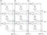
相应的,本发明还提供一种存储阵列结构,参考图6、图11至图14,所述存储阵列结构包括:若干个沿行方向和列方向分布的前述的存储单元,所述行方向与列方向相互垂直,其中,处于同一列存储单元的第一二极管区的第一阱区104相连通,处于同一列存储单元的第二二极管区的第一阱区104相连通,处于同一列存储单元的第三二极管区的第二阱区105相连通,处于同一列存储单元的第四二极管区的第二阱区105相连通;字线111,同一字线111对应电连接处于同一行的存储单元的RRAM器件;复位线134,同一复位线134对应电连接处于同一列存储单元的第一二极管区或者第二二极管区的第一阱区104;位线135,同一位线135对应电连接处于同一列存储单元的第三二极管区或者第四二极管区的第二阱区105。Correspondingly, the present invention also provides a memory array structure. Referring to FIG. 6 and FIG. 11 to FIG. 14 , the memory array structure includes: a plurality of the aforementioned memory cells distributed along the row direction and the column direction. The column directions are perpendicular to each other, wherein the first
其中,所述存储单元包括:基底101,所述基底101包括沿行方向依次排列的第一二极管区、第二二极管区、第三二极管区以及第四二极管区;位于所述第一二极管区以及第二二极管区的基底101内的第一阱区104;位于所述第三二极管区以及第四二极管区的基底101内的第二阱区105,且所述第二阱区105的掺杂类型与所述第一阱区104的掺杂类型不同;分别位于所述第一阱区104以及第二阱区105上的掺杂导电区106;位于所述基底101内的深沟槽隔离结构103,其中,所述深沟槽隔离结构106电隔离所述第一二极管区的第一阱区104与所述第二二极管区的第一阱区104,电隔离所述第三二极管区的第二阱区105与所述第四二极管区的第二阱区105,电隔离所述第一二极管区的掺杂导电区106与所述第二二极管区的掺杂导电区106,电隔离所述第三二极管区与所述第四二极管区的掺杂导电区106;RRAM器件110,所述RRAM器件110电连接所述第二二极管区的掺杂导电区106以及第三二极管区的掺杂导电区106。Wherein, the storage unit includes: a substrate 101, the substrate 101 includes a first diode region, a second diode region, a third diode region and a fourth diode region arranged in sequence along the row direction; The first well region 104 located in the substrate 101 of the first diode region and the second diode region; the second well region 104 located in the substrate 101 of the third diode region and the fourth diode region Well region 105, and the doping type of the second well region 105 is different from the doping type of the first well region 104; the doping types located on the first well region 104 and the second well region 105 respectively are conductive region 106; deep trench isolation structure 103 in the substrate 101, wherein the deep trench isolation structure 106 electrically isolates the first well region 104 of the first diode region from the second diode The first well region 104 of the tube region electrically isolates the second well region 105 of the third diode region and the second well region 105 of the fourth diode region, and electrically isolates the first diode The doped conductive region 106 of the second diode region and the doped conductive region 106 of the second diode region are electrically isolated from the doped conductive region 106 of the third diode region and the fourth diode region; RRAM Device 110, the RRAM device 110 is electrically connected to the doped conductive region 106 of the second diode region and the doped conductive region 106 of the third diode region.
以下将结合附图对本发明实施例提供的存储阵列结构进行详细说明。The memory array structure provided by the embodiments of the present invention will be described in detail below with reference to the accompanying drawings.
有关所述存储单元的详细描述可参考前述实施例的说明,在此不再赘述。For the detailed description of the storage unit, reference may be made to the description of the foregoing embodiments, and details are not repeated here.
本实施例中,所述存储阵列结构还包括:位于所述基底101内与所述复位线134电连接的复位线选通二极管,以及与所述位线135电连接的位线选通二极管,且所述复位选通二极管以及位线选通二极管沿行方向分布;In this embodiment, the memory array structure further includes: a reset line gate diode located in the
其中,所述复位线选通二极管包括:位于所述基底101内的复位线选通阱区114,与处于同一列的存储单元的第一阱区104相连通;位于所述复位线选通阱区114上的复位线掺杂导电区124,且所述复位线掺杂导电区124的掺杂类型与所述复位线选通阱区114的掺杂类型相同,所述复位线掺杂导电区124与所述复位线134电连接;Wherein, the reset line gate diode includes: a reset line
所述位线选通二极管包括:位于所述基底101内的位线选通阱区115,与处于同一列的存储单元的第二阱区105相连通;位于所述位线选通阱区115上的位线掺杂导电区125,且所述位线掺杂导电区125的掺杂类型与所述位线选通阱区115的掺杂类型相同,所述位线掺杂导电区125与所述位线135电连接The bit line gate diode includes: a bit line
所述存储单元还包括:所述导电插塞108,所述导电插塞108分别位于所述第二二极管区以及第三二极管区的掺杂导电区106上;电连接所述导电插塞108的金属层109,其中,所述RRAM器件110位于所述金属层109上;其中,所述复位线134与所述金属层109处于同层,且所述位线135与所述金属层109处于同层。The storage unit further includes: the
相邻列的存储单元通过所述深沟槽隔离结构103电隔离;所述存储阵列结构还包括:位于所述基底101内的浅沟槽隔离结构100,所述浅沟槽隔离结构100电隔离相邻行的存储单元的掺杂导电区106。Memory cells in adjacent columns are electrically isolated by the deep
图15示出了本实施例提供的存储阵列结构的等效电路结构示意图,其中,第二二极管区的二极管、第三二极管区的二极管、以及RRAM器件等效电阻构成2D1R结构;字线WLn-1、WLn以及WLn+1与RRAM器件等效电阻电连接;位线BLn-1、BLn、BLn+1与2D1R结构中的一个二极管电连接;复位线Reset Ln-1、Reset Ln、Reset Ln+1与2D1R结构中的另一个二极管电连接。15 shows a schematic diagram of an equivalent circuit structure of the memory array structure provided in this embodiment, wherein the diodes in the second diode region, the diodes in the third diode region, and the equivalent resistance of the RRAM device form a 2D1R structure; The word lines WLn-1, WLn and WLn+1 are electrically connected to the equivalent resistance of the RRAM device; the bit lines BLn-1, BLn, BLn+1 are electrically connected to a diode in the 2D1R structure; the reset lines Reset Ln-1, Reset Ln , Reset Ln+1 is electrically connected to another diode in the 2D1R structure.
下表示出了本实施例提供的存储阵列结构的工作原理。所述存储阵列结构具有选择状态以及非选择状态两种工作状态。The following table shows the working principle of the storage array structure provided in this embodiment. The storage array structure has two working states: a selection state and a non-selection state.
在选择状态下,进行设置操作时,字线WL接设置电压Vset,位线BL接地(0V),复位线Reset L悬置;进行重置操作时,字线WL接地,位线BL悬置,复位线Reset L接复位电压Vreset;进行读取操作时,字线WL接读取电压Vread,位线BL接地,复位线Reset L悬置。In the selection state, during the setting operation, the word line WL is connected to the set voltage Vset, the bit line BL is grounded (0V), and the reset line Reset L is suspended; when the reset operation is performed, the word line WL is grounded, and the bit line BL is suspended, The reset line Reset L is connected to the reset voltage Vreset; during the read operation, the word line WL is connected to the read voltage Vread, the bit line BL is grounded, and the reset line Reset L is suspended.
在非选择状态下,进行设置操作时,字线WL、位线BL以及复位线Reset L均悬置;进行重置操作时,字线WL以及位线BL悬置,复位线Reset L接地;进行读取操作时,字线WL、位线BL以及复位线Beset L均悬置。In the non-selected state, when the setting operation is performed, the word line WL, the bit line BL and the reset line Reset L are all suspended; when the reset operation is performed, the word line WL and the bit line BL are suspended, and the reset line Reset L is grounded; During a read operation, the word line WL, the bit line BL and the reset line Beset L are all suspended.

虽然本发明披露如上,但本发明并非限定于此。任何本领域技术人员,在不脱离本发明的精神和范围内,均可作各种更动与修改,因此本发明的保护范围应当以权利要求所限定的范围为准。Although the present invention is disclosed above, the present invention is not limited thereto. Any person skilled in the art can make various changes and modifications without departing from the spirit and scope of the present invention. Therefore, the protection scope of the present invention should be based on the scope defined by the claims.
Claims (20)
Priority Applications (2)
| Application Number | Priority Date | Filing Date | Title |
|---|---|---|---|
| CN201710176063.6ACN108630722B (en) | 2017-03-22 | 2017-03-22 | Memory cell and method of forming the same, memory array structure and method of forming the same |
| US15/927,665US10741610B2 (en) | 2017-03-22 | 2018-03-21 | Memory cells and memory array structures including RRAM, and fabrication methods thereof |
Applications Claiming Priority (1)
| Application Number | Priority Date | Filing Date | Title |
|---|---|---|---|
| CN201710176063.6ACN108630722B (en) | 2017-03-22 | 2017-03-22 | Memory cell and method of forming the same, memory array structure and method of forming the same |
Publications (2)
| Publication Number | Publication Date |
|---|---|
| CN108630722A CN108630722A (en) | 2018-10-09 |
| CN108630722Btrue CN108630722B (en) | 2020-10-30 |
Family
ID=63582900
Family Applications (1)
| Application Number | Title | Priority Date | Filing Date |
|---|---|---|---|
| CN201710176063.6AActiveCN108630722B (en) | 2017-03-22 | 2017-03-22 | Memory cell and method of forming the same, memory array structure and method of forming the same |
Country Status (2)
| Country | Link |
|---|---|
| US (1) | US10741610B2 (en) |
| CN (1) | CN108630722B (en) |
Citations (3)
| Publication number | Priority date | Publication date | Assignee | Title |
|---|---|---|---|---|
| CN1505043A (en)* | 2002-12-05 | 2004-06-16 | ������������ʽ���� | Nonvolatile memory cell and nonvolatile semiconductor memory device |
| CN101419940A (en)* | 2007-10-22 | 2009-04-29 | 旺宏电子股份有限公司 | Method for producing a memory cell combination and memory cell combination |
| CN102376359A (en)* | 2010-08-20 | 2012-03-14 | 庄建祥 | One-time programmable, electric fuse, programmable resistive memory and method |
Family Cites Families (9)
| Publication number | Priority date | Publication date | Assignee | Title |
|---|---|---|---|---|
| US5559368A (en)* | 1994-08-30 | 1996-09-24 | The Regents Of The University Of California | Dynamic threshold voltage mosfet having gate to body connection for ultra-low voltage operation |
| AU2003201760A1 (en)* | 2002-04-04 | 2003-10-20 | Kabushiki Kaisha Toshiba | Phase-change memory device |
| US20090185410A1 (en)* | 2008-01-22 | 2009-07-23 | Grandis, Inc. | Method and system for providing spin transfer tunneling magnetic memories utilizing unidirectional polarity selection devices |
| US8134137B2 (en)* | 2008-06-18 | 2012-03-13 | Micron Technology, Inc. | Memory device constructions, memory cell forming methods, and semiconductor construction forming methods |
| US20100118602A1 (en)* | 2008-11-13 | 2010-05-13 | Seagate Technology Llc | Double source line-based memory array and memory cells thereof |
| US7911833B2 (en)* | 2009-07-13 | 2011-03-22 | Seagate Technology Llc | Anti-parallel diode structure and method of fabrication |
| US8488364B2 (en)* | 2010-08-20 | 2013-07-16 | Shine C. Chung | Circuit and system of using a polysilicon diode as program selector for resistive devices in CMOS logic processes |
| WO2013044612A1 (en)* | 2011-09-29 | 2013-04-04 | Tsinghua University | Vertical selection transistor, memory cell, and three-dimensional memory array structure and method for fabricating the same |
| US9583536B2 (en)* | 2015-07-23 | 2017-02-28 | Macronix International Co., Ltd. | Memory device and method for manufacturing the same |
- 2017
- 2017-03-22CNCN201710176063.6Apatent/CN108630722B/enactiveActive
- 2018
- 2018-03-21USUS15/927,665patent/US10741610B2/enactiveActive
Patent Citations (3)
| Publication number | Priority date | Publication date | Assignee | Title |
|---|---|---|---|---|
| CN1505043A (en)* | 2002-12-05 | 2004-06-16 | ������������ʽ���� | Nonvolatile memory cell and nonvolatile semiconductor memory device |
| CN101419940A (en)* | 2007-10-22 | 2009-04-29 | 旺宏电子股份有限公司 | Method for producing a memory cell combination and memory cell combination |
| CN102376359A (en)* | 2010-08-20 | 2012-03-14 | 庄建祥 | One-time programmable, electric fuse, programmable resistive memory and method |
Also Published As
| Publication number | Publication date |
|---|---|
| US10741610B2 (en) | 2020-08-11 |
| US20180277600A1 (en) | 2018-09-27 |
| CN108630722A (en) | 2018-10-09 |
Similar Documents
| Publication | Publication Date | Title |
|---|---|---|
| CN113257850B (en) | Resistive memory cell and related array structure thereof | |
| US9530824B2 (en) | Monolithic three dimensional memory arrays with staggered vertical bit line select transistors and methods therfor | |
| US10026747B2 (en) | Non-volatile memory device with first gate structure in memory cell region and second gate structure in peripheral circuit region and non-volatile memory system including the same | |
| CN104752456B (en) | Metal wire connection for improved RRAM reliability, semiconductor arrangement including same and manufacturing method thereof | |
| US9595530B1 (en) | Methods and apparatus for vertical bit line structures in three-dimensional nonvolatile memory | |
| CN104900804B (en) | RRAM cell structure with conductive etch stop layer | |
| CN111564449B (en) | Memory element and manufacturing method thereof | |
| US7382646B2 (en) | Memory architecture containing a high density memory array of semi-volatile or non-volatile memory elements | |
| CN101625893B (en) | Strap-contact scheme for compact array of memory cells | |
| TWI587448B (en) | Integrated circuit device and method of manufacturing same | |
| US10355129B2 (en) | Vertical transistors with sidewall gate air gaps and methods therefor | |
| CN102637686A (en) | Nonvolatile semiconductor memory device and method of manufacturing the same | |
| US10128313B2 (en) | Non-volatile memory device and structure thereof | |
| KR102320645B1 (en) | A memory cell comprising a transistor having a GaP channel material | |
| TWI624933B (en) | Nonvolatile semiconductor memory | |
| CN115000045A (en) | Vertical contacts for semiconductor devices | |
| US10541273B2 (en) | Vertical thin film transistors with isolation | |
| CN108431978A (en) | Monolithic 3D memory array formed using sacrificial polysilicon pillars | |
| KR20230086451A (en) | Memory device and manufacturing method of the memory device | |
| CN108630722B (en) | Memory cell and method of forming the same, memory array structure and method of forming the same | |
| CN105321563B (en) | Nonvolatile semiconductor memory | |
| US20170133063A1 (en) | Memory device with reduced-resistance interconnect | |
| US11380387B1 (en) | Multiplexor for a semiconductor device | |
| CN117016049A (en) | Three-dimensional memory device and method of forming the same | |
| TWI538109B (en) | Integrated circuit and method for fabricating and operating the same |
Legal Events
| Date | Code | Title | Description |
|---|---|---|---|
| PB01 | Publication | ||
| PB01 | Publication | ||
| SE01 | Entry into force of request for substantive examination | ||
| SE01 | Entry into force of request for substantive examination | ||
| GR01 | Patent grant | ||
| GR01 | Patent grant |