CN108572142B - Optical computing optical coherent imaging system with high signal-to-noise ratio - Google Patents
Optical computing optical coherent imaging system with high signal-to-noise ratioDownload PDFInfo
- Publication number
- CN108572142B CN108572142BCN201710138075.XACN201710138075ACN108572142BCN 108572142 BCN108572142 BCN 108572142BCN 201710138075 ACN201710138075 ACN 201710138075ACN 108572142 BCN108572142 BCN 108572142B
- Authority
- CN
- China
- Prior art keywords
- optical
- light
- emitted
- circulator
- signal
- Prior art date
- Legal status (The legal status is an assumption and is not a legal conclusion. Google has not performed a legal analysis and makes no representation as to the accuracy of the status listed.)
- Active
Links
Images


Classifications
- G—PHYSICS
- G01—MEASURING; TESTING
- G01N—INVESTIGATING OR ANALYSING MATERIALS BY DETERMINING THEIR CHEMICAL OR PHYSICAL PROPERTIES
- G01N21/00—Investigating or analysing materials by the use of optical means, i.e. using sub-millimetre waves, infrared, visible or ultraviolet light
- G01N21/17—Systems in which incident light is modified in accordance with the properties of the material investigated
- G—PHYSICS
- G01—MEASURING; TESTING
- G01N—INVESTIGATING OR ANALYSING MATERIALS BY DETERMINING THEIR CHEMICAL OR PHYSICAL PROPERTIES
- G01N21/00—Investigating or analysing materials by the use of optical means, i.e. using sub-millimetre waves, infrared, visible or ultraviolet light
- G01N21/01—Arrangements or apparatus for facilitating the optical investigation
Landscapes
- Physics & Mathematics (AREA)
- Health & Medical Sciences (AREA)
- Life Sciences & Earth Sciences (AREA)
- Chemical & Material Sciences (AREA)
- Analytical Chemistry (AREA)
- Biochemistry (AREA)
- General Health & Medical Sciences (AREA)
- General Physics & Mathematics (AREA)
- Immunology (AREA)
- Pathology (AREA)
- Investigating Or Analysing Materials By Optical Means (AREA)
Abstract
Translated fromChinese
Description
Translated fromChinese技术领域technical field
本发明涉及一种光学相干成像系统(Optical Coherence Tomograpgy,简称OCT),特别是关于一种高信噪比的光计算光学相干成像系统,属于生物医学光子学技术领域。The invention relates to an optical coherence imaging system (Optical Coherence Tomography, OCT for short), in particular to an optical computing optical coherence imaging system with high signal-to-noise ratio, which belongs to the technical field of biomedical photonics.
背景技术Background technique
光学相干成像技术已经由传统的时域光学相干成像(Time Domain-OCT,简称TD-OCT)发展为频域光学相干成像(Fourier Domain-OCT,简称FD-OCT)。随后出现了基于光计算的光学相干成像系统,该光学相干成像系统最大的优势就是速度快。但是,现有技术中基于光计算的光学相干成像系统信噪比略低(<50dB)。对于生物样品的成像,信噪比是至关重要的指标。无论成像速度多快,如果图像信号淹没在噪声里,那么实际使用中就会受到很多限制。Optical coherence imaging technology has been developed from traditional time domain optical coherence imaging (Time Domain-OCT, TD-OCT for short) to frequency domain optical coherence imaging (Fourier Domain-OCT, FD-OCT for short). Then an optical coherent imaging system based on light calculation appeared, and the biggest advantage of this optical coherent imaging system is its speed. However, the signal-to-noise ratio of optical coherent imaging systems based on optical computing in the prior art is slightly lower (<50 dB). For the imaging of biological samples, the signal-to-noise ratio is a crucial metric. No matter how fast the imaging speed is, if the image signal is drowned in noise, there will be many limitations in practical use.
发明内容SUMMARY OF THE INVENTION
针对上述问题,本发明的目的是提供一种高信噪比的光计算光学相干成像系统。In view of the above problems, the purpose of the present invention is to provide an optical computational optical coherence imaging system with high signal-to-noise ratio.
为实现上述目的,本发明采取以下技术方案:一种高信噪比的光计算光学相干成像系统,其特征在于,包括宽带光源、两耦合器、信号发生装置、两光相位调制器、色散器件、四环形器、二维扫描系统、平衡探测器、滤波器、解调器和计算机;其中,第一光相位调制器经所述信号发生装置产生形状为cos(at2)信号进行驱动,第二光相位调制器经所述信号产生装置产生形状为cos(at2+2πf0t)信号进行驱动,其中,t为时间,a和f0为常数;所述宽带光源发出的直流宽带光经第一耦合器分为参考光和测量光;所述参考光经所述第一光相位调制器进行调制后通过第一环形器发射到所述色散器件,经所述色散器件出射的光经第二环形器发射到所述第二光相位调制器再次进行调制后发射到第三环形器,经所述第三环形器出射的光经一聚焦透镜发射到一反射镜后沿着原光路返回并经所述第三环形器发射到第二耦合器;测量光经所述第二环形器进入所述色散器件,所述色散器件出射的光经所述第一环形器发射到第四环形器,经所述第四环形器出射的光经一聚焦透镜进入所述二维扫描系统,所述二维扫描系统用于将测量光反射到待测样品,经所述待测样品反射的光沿着原光路返回经所述第四环形器进入所述第二耦合器与参考光发生干涉;经所述第二耦合器出射的干涉光依次经所述平衡探测器、滤波器和解调器发送到所述计算机得到待测样品的结构图像。In order to achieve the above object, the present invention adopts the following technical solutions: a high signal-to-noise ratio optical computing optical coherent imaging system, characterized in that it includes a broadband light source, two couplers, a signal generating device, two optical phase modulators, and a dispersion device. , four circulators, two-dimensional scanning systems, balanced detectors, filters, demodulators and computers; wherein, the first optical phase modulator is driven by the signal generating device to generate a cos(at2 ) signal, and the first optical phase modulator is driven by The two-optical phase modulator is driven by a signal with a shape of cos(at2 +2πf0 t) generated by the signal generating device, where t is time, and a and f0 are constants; the DC broadband light emitted by the broadband light source is The first coupler is divided into reference light and measurement light; the reference light is modulated by the first optical phase modulator and then emitted to the dispersion device through the first circulator, and the light emitted through the dispersion device is transmitted through the first circulator. The second circulator emits to the second optical phase modulator, modulates it again, and then emits it to the third circulator. The light emitted by the third circulator is emitted to a reflector through a focusing lens, and then returns along the original optical path. It is emitted to the second coupler through the third circulator; the measurement light enters the dispersion device through the second circulator, and the light emitted from the dispersion device is emitted to the fourth circulator through the first circulator, The light emitted by the fourth circulator enters the two-dimensional scanning system through a focusing lens, and the two-dimensional scanning system is used to reflect the measurement light to the sample to be tested, and the light reflected by the sample to be tested goes along the The original optical path returns through the fourth circulator and enters the second coupler to interfere with the reference light; the interference light exiting through the second coupler is sequentially sent to the balanced detector, filter and demodulator. The computer obtains a structural image of the sample to be tested.
优选地,所述色散器件采用色散光纤。Preferably, the dispersion device adopts a dispersion fiber.
为实现上述目的,本发明还可以采取以下技术方案:一种高信噪比的光计算光学相干成像系统,其特征在于,包括宽带光源、两耦合器、信号发生装置、两光相位调制器、两色散器件、两环形器、二维扫描系统、平衡探测器、滤波器、解调器和计算机;其中,第一光相位调制器经所述信号发生装置产生形状为cos(at2)信号进行驱动,第二光相位调制器经所述信号产生装置产生形状为cos(at2+2πf0t)信号进行驱动,其中,t为时间,a和f0为常数;所述宽带光源发出的直流宽带光经第一耦合器分为参考光和测量光;参考光发射到所述第一光相位调制器进行调制后发射到第一色散器件,经所述第一色散器件出射的光发射到所述第二光相位调制器再次调制后发射到第一环形器,经所述第一环形器出射的光经一聚焦透镜会聚后发射到一反射镜后沿着原光路返回经所述第一环形器发射到第二耦合器;测量光经第二色散器件发射到第二环形器,经所述第二环形器出射的光经一聚焦透镜进入所述二维扫描系统,所述二维扫描系统用于将测量光反射到待测样品,经所述待测样品反射的光沿着原光路返回经所述第二环形器进入所述第二耦合器与参考光发生干涉;经所述第二耦合器出射的干涉光依次经所述平衡探测器、滤波器和解调器发送到所述计算机得到待测样品的结构图像。In order to achieve the above object, the present invention can also adopt the following technical solutions: a high signal-to-noise ratio optical computing optical coherent imaging system, characterized in that it includes a broadband light source, two couplers, a signal generating device, two optical phase modulators, Two dispersive devices, two circulators, two-dimensional scanning systems, balanced detectors, filters, demodulators and computers; wherein, the first optical phase modulator generates a cos(at2 ) signal through the signal generating device for processing drive, the second optical phase modulator is driven by the signal generating device to generate a signal with a shape of cos(at2 +2πf0 t), where t is time, and a and f0 are constants; the direct current emitted by the broadband light source The broadband light is divided into reference light and measurement light through the first coupler; the reference light is emitted to the first optical phase modulator for modulation and then emitted to the first dispersion device, and the light emitted by the first dispersion device is emitted to the first dispersion device. The second optical phase modulator is modulated again and then emitted to the first circulator. The light emitted by the first circulator is condensed by a focusing lens and then emitted to a reflector, and then returns to the first ring along the original optical path. The measurement light is emitted to the second circulator through the second dispersion device, and the light emitted through the second circulator enters the two-dimensional scanning system through a focusing lens, and the two-dimensional scanning system It is used to reflect the measurement light to the sample to be tested, and the light reflected by the sample to be tested returns along the original optical path and enters the second coupler through the second circulator to interfere with the reference light; The interference light emitted by the coupler is sequentially sent to the computer through the balanced detector, the filter and the demodulator to obtain a structural image of the sample to be tested.
优选地,所述第一色散器件和第二色散器件结构完全相同,均包括环形器和光纤布拉格光栅。Preferably, the structures of the first dispersion device and the second dispersion device are completely the same, and both include a circulator and a fiber Bragg grating.
优选地,所述第一光相位调制器和第二光相位调制器采用电光相位调制器。Preferably, the first optical phase modulator and the second optical phase modulator are electro-optical phase modulators.
优选地,所述信号发生装置包括波形发生器,所述波形发生器与所述第一光相位调制器之间设置第一射频放大器,所述波形发生器与所述第二光相位调制器之间设置第二射频放大器。Preferably, the signal generating device includes a waveform generator, a first radio frequency amplifier is arranged between the waveform generator and the first optical phase modulator, and a first radio frequency amplifier is arranged between the waveform generator and the second optical phase modulator. A second radio frequency amplifier is arranged between.
优选地,所述宽带光源的工作波段采用850nm、1064nm、1310nm和1550nm中的一种。Preferably, the working wavelength band of the broadband light source adopts one of 850 nm, 1064 nm, 1310 nm and 1550 nm.
本发明由于采取以上技术方案,具有以下优点:1、本发明在马赫-曾德耳干涉仪的参考臂上设置光相位调制器,相对于现有基于光计算的光学相干成像系统采用的光强度调制器,具有以下优势:1)光相位调制器不需要光强度调制器所必需的偏置电压,同时也避免了温漂的问题;2)光相位调制器的插损通常比光强度调制器的插损低3dB,降低了光的损耗;3)马赫-曾德耳干涉仪的参考臂上设置光相位调制器的插损只会影响到此臂上的光功率而不是总的光功率,大大节约了总的光功率,因此能够直接增强系统的光功率,提高整个系统信噪比。2、本发明由于设置有第二个光相位调制器和滤波器,因此可以将光计算信号的变频率载波转换成固定频率载波,降低了光信号的探测带宽,提高信噪比。3、本发明的整个光路不但结构简单,而且均可以采用全光纤器件,使系统的能量利用率、稳定性、集成度更高。4、本发明由于设置有第二耦合器,经第二耦合器出射的同比例的光经平衡探测器接收,其中的直流信号以及共模噪声均被平衡探测器去除,有效提高信噪比。综上所述,本发明从两方面极大地提高了系统信噪比,一方面是改变了光调制器的类型以及位置,提高了光功率;另一方面是将随时间变化的载波频率固定在了某一特定频率,减小了探测带宽,这样可将信噪比提高至少30dB,达到整个系统应有的散粒噪声极限。本发明具有结构简单、全光纤化、工作稳定的特点,可以广泛应用于光学相干成像中。The present invention has the following advantages due to the adoption of the above technical solutions: 1. The present invention sets an optical phase modulator on the reference arm of the Mach-Zehnder interferometer, compared with the light intensity adopted by the existing optical coherence imaging system based on optical calculation. The modulator has the following advantages: 1) the optical phase modulator does not require the necessary bias voltage of the optical intensity modulator, and also avoids the problem of temperature drift; 2) the insertion loss of the optical phase modulator is usually higher than that of the optical intensity modulator The insertion loss is 3dB lower, which reduces the loss of light; 3) The insertion loss of the optical phase modulator set on the reference arm of the Mach-Zehnder interferometer will only affect the optical power on this arm instead of the total optical power, The total optical power is greatly saved, so it can directly enhance the optical power of the system and improve the signal-to-noise ratio of the entire system. 2. Since the present invention is provided with a second optical phase modulator and filter, the variable frequency carrier of the optical computing signal can be converted into a fixed frequency carrier, which reduces the detection bandwidth of the optical signal and improves the signal-to-noise ratio. 3. The entire optical path of the present invention is not only simple in structure, but also can use all-fiber devices, so that the energy utilization rate, stability and integration of the system are higher. 4. Since the present invention is provided with a second coupler, the same proportion of light emitted by the second coupler is received by the balanced detector, and the DC signal and common mode noise in it are removed by the balanced detector, which effectively improves the signal-to-noise ratio. To sum up, the present invention greatly improves the signal-to-noise ratio of the system from two aspects: on the one hand, the type and position of the optical modulator are changed to improve the optical power; on the other hand, the carrier frequency that changes with time is fixed at A certain frequency is selected, and the detection bandwidth is reduced, which can increase the signal-to-noise ratio by at least 30dB, and reach the due shot noise limit of the whole system. The invention has the characteristics of simple structure, all-fiberization and stable operation, and can be widely used in optical coherent imaging.
附图说明Description of drawings
图1为本发明的光计算光学相干成像系统实施例1的结构示意图;FIG. 1 is a schematic structural diagram of
图2为本发明的光计算光学相干成像系统实施例2的结构示意图;2 is a schematic structural diagram of
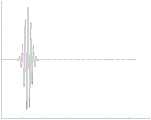
图3为本发明采用镜面作为样品时,理论计算得到的平衡探测器输出信号示意图;3 is a schematic diagram of the output signal of a balanced detector obtained by theoretical calculation when a mirror surface is used as a sample in the present invention;
图4为本发明采用镜面作为样品时,实验测得的平衡探测器输出信号示意图。FIG. 4 is a schematic diagram of an output signal of a balanced detector measured experimentally when a mirror surface is used as a sample in the present invention.
具体实施方式Detailed ways
以下结合附图来对本发明进行详细的描绘。然而应当理解,附图的提供仅为了更好地理解本发明,它们不应该理解成对本发明的限制。在本发明的描述中,需要理解的是,术语“第一”、“第二”等仅仅是用于描述的目的,而不能理解为指示或暗示相对重要性。The present invention will be described in detail below with reference to the accompanying drawings. It should be understood, however, that the accompanying drawings are provided only for a better understanding of the present invention, and they should not be construed to limit the present invention. In the description of the present invention, it should be understood that the terms "first", "second", etc. are only used for the purpose of description, and should not be construed as indicating or implying relative importance.
在现有技术公开的专利文件中记载的基于光计算的光学相干成像系统所输出的信号是cos(at2)*S(ω=t/D0),该信号的包络就是待测样品的一线空间结构信息,其中,“*”为卷积运算符号,a为一常数,t为时间,S(ω)为OCT干涉光谱形状,D0为色散量,具体详见申请号为201510107496.7的具体实施方式记载,在此不作赘述。The signal output by the optical coherence imaging system based on light calculation described in the patent documents disclosed in the prior art is cos(at2 )*S(ω=t/D0 ), and the envelope of the signal is the sample to be tested. One-line spatial structure information, where "*" is the convolution operation symbol, a is a constant, t is time, S(ω) is the shape of the OCT interference spectrum, and D0 is the amount of dispersion. For details, please refer to the application number 201510107496.7 for details. Embodiments are described, and are not repeated here.
卷积cos(at2)*S(ω=t/D0)当中有意义的是卷积结果的包络(代表所测样品的一线空间结构信息),该信号的载波是无意义的。而且这个载波的频率是随时间变化的,导致增加了光信号的探测带宽,进而引起信噪比降低(散粒噪声极限情况下,信噪比反比于探测带宽)。因此,要减小带宽,提高信噪比,还需要将代表卷积cos(at2)*S(ω=t/D0)的光信号输入到另一个光调制器中,用一个与信号载波存在固定频率差f0的信号对其调制,最后就得到cos(at2+2πf0t)[cos(at2)*S(ω=t/D0)]。根据积化和差公式,调制后的信号分成和频与差频两部分,选取合适的参数可以保证和频部分与差频部分在频谱上无交集,采用滤波器将和频部分移除,留下的差频部分的载波频率即是f0,这样就大大减小了探测带宽,显著提高了信噪比,该差频信号的包络就是所测样品的一线空间结构信息,下面通过两个具体实施例详细说明可以明显提高信噪比的光计算光学相干成像系统的光路结构。What is meaningful in the convolution cos(at2 )*S(ω=t/D0 ) is the envelope of the convolution result (representing the one-line spatial structure information of the measured sample), and the carrier of the signal is meaningless. Moreover, the frequency of this carrier varies with time, resulting in an increase in the detection bandwidth of the optical signal, which in turn causes a decrease in the signal-to-noise ratio (in the case of the shot noise limit, the signal-to-noise ratio is inversely proportional to the detection bandwidth). Therefore, in order to reduce the bandwidth and improve the signal-to-noise ratio, it is also necessary to input the optical signal representing the convolution cos(at2 )*S(ω=t/D0 ) into another optical modulator, and use an optical signal with the signal carrier A signal with a fixed frequency difference f0 modulates it, and finally cos(at2 +2πf0 t)[cos(at2 )*S(ω=t/D0 )] is obtained. According to the integral sum-difference formula, the modulated signal is divided into two parts, the sum-frequency part and the difference-frequency part. Selecting appropriate parameters can ensure that the sum-frequency part and the difference-frequency part have no overlap in the spectrum. The filter is used to remove the sum-frequency part and leave the The carrier frequency of the beat frequency part below is f0 , which greatly reduces the detection bandwidth and significantly improves the signal-to-noise ratio. The envelope of the beat frequency signal is the one-line spatial structure information of the measured sample. The specific embodiments describe in detail the optical path structure of the optical computational optical coherence imaging system that can significantly improve the signal-to-noise ratio.
实施例1:Example 1:
如图1所示,本实施例提供的光计算光学相干成像系统,包括一光计算系统和一图像显示系统。光计算系统包括宽带光源1、第一耦合器2、信号发生装置3、第一光相位调制器4、第二光相位调制器5、第一~第四环形器6~9、色散器件10、第一聚焦透镜11、第二聚焦透镜12、第二耦合器13、二维扫描系统14和反射镜19,图像显示系统包括平衡探测器15、滤波器16、解调器17和计算机18。其中,第一光相位调制器4经信号发生装置3产生形状为cos(at2)信号进行驱动,第二光相位调制器5经信号产生装置3产生形状为cos(at2+2πf0t)信号进行驱动,本实施例的色散器件10可以采用色散光纤。As shown in FIG. 1 , the optical computing optical coherence imaging system provided in this embodiment includes an optical computing system and an image display system. The optical computing system includes a
工作波段为1550nm的宽带光源1发出的直流宽带光经第一耦合器2分为参考光和测量光;The DC broadband light emitted by the
参考光发射到第一光相位调制器4进行调制后经第一环形器6发射到色散器件10,经色散器件10出射的光经第二环形器7发射到第二光相位调制器5再次进行调制,调制后的光经第三环形器8发射到第一聚焦透镜11,经第一聚焦透镜11会聚后的光信号发射到反射镜19后沿着原光路返回经第三环形器8发射到第二耦合器13;The reference light is emitted to the first optical phase modulator 4 for modulation, and then emitted to the
测量光经第二环形器7进入色散器件10,色散器件10出射的光经第一环形器6发射到第四环形器9,经第四环形器9出射的光通过第二聚焦透镜12进入二维扫描系统14,二维扫描系统14将测量光反射到待测样品20的不同位置,经待测样品20不同位置、不同深度反射的光沿着原光路返回进入第四环形器9,经第四环形器9出射的光发射到第二耦合器13与参考光发生干涉;The measurement light enters the
经第二耦合器13出射的干涉光发射到平衡探测器15,平衡探测器15将光信号转换为电信号后发送到滤波器16,滤波器16将和频部分移除,仅保留差频部分。经滤波器16滤波后的信号进入解调器17得到包络信号,包络信号发送到计算机18得到样品的结构图像。The interference light emitted by the second coupler 13 is emitted to the
实施例2:Example 2:
如图2所示,本实施例与实施例1的光路结构和光路器件基本相同,不同的是实施例1是参考光和测量光同时使用一个色散器件10,本实施例中参考光和测量光单独使用各自的色散器件,两个色散器件结构和功能完全相同,第一色散器件21采用一环形器211和一光纤布拉格光栅212,第二色散器件22采用一环形器221和一光纤布拉格光栅222。本实施例的光路传播具体过程为:As shown in FIG. 2 , the optical path structure and optical path device of this embodiment are basically the same as those of
宽带光源1发出的直流宽带光经第一耦合器2分为参考光和测量光;The DC broadband light emitted by the
参考光发射到第一光相位调制器4进行调制后发射到环形器211,经环形器211出射的光信号经光纤布拉格光栅212反射返回环形器211,将环形器211出射的光发射到第二光相位调制器5进行调制后发射到第三环形器8,经第三环形器8出射的光经第一聚焦透镜11会聚后发射到反射镜19后沿着原光路返回经第三环形器8发射到第二耦合器13;The reference light is transmitted to the first optical phase modulator 4 for modulation and then transmitted to the
测量光发射到环形器221,经环形器221出射的光发射到光纤布拉格光栅222反射进入环形器221,经环形器221出射的光发射到第四环形器9,经第四环形器9出射的光经第二聚焦透镜12进入二维扫描系统14,二维扫描系统14将测量光反射到待测样品20的不同位置,经待测样品20不同位置、不同深度反射的光沿着原光路返回进入第四环形器9,经第四环形器9出射的光发射到第二耦合器13与参考光发生干涉;The measurement light is emitted to the
经第二耦合器13出射的干涉光经平衡探测器15接收,平衡探测器15将光信号转换为电信号后发送到滤波器16,滤波器16将和频部分移除,仅保留差频部分。经滤波器16滤波后的信号进入解调器17得到包络信号,包络信号发送到计算机18得到样品的结构图像。The interference light emitted by the second coupler 13 is received by the
如图3和图4所示,当将镜面作为待测样品20时,采用本发明系统经试验证明,平衡探测器15输出信号的实验结果与理论计算结果一致,因此证明本发明的光计算光学相干成像系统的原理正确可行。As shown in FIGS. 3 and 4 , when the mirror surface is used as the sample to be tested 20, the system of the present invention is used to prove that the experimental result of the output signal of the
上述各实施例中,第一光相位调制器4和第二光相位调制器5均可以采用电光相位调制器。In the above embodiments, both the first optical phase modulator 4 and the second
上述各实施例中,第一耦合器2和第二耦合器13的耦合比根据实际试验需要进行设置,在此不做限定,本发明实施例中的第一耦合器2的耦合比参数为10/90,第二耦合器13的耦合比例参数为50/50。In the above-mentioned embodiments, the coupling ratio of the
上述各实施例中,信号发生装置3可以采用波形发生器31,由于现有的光相位调制器的半波电压显著大于波形发生器31输出电压的幅度,因此波形发生器31与第一光相位调制器4、第二光相位调制器5之间可以设置第一射频放大器32、第二射频放大器33用于提高调制深度;波形发生器31分别与第一射频放大器32和第二射频放大器33用于驱动第一光相位调制器4、第二光相位调制器5以便将输入的光分别调制为波形cos(at2)、cos(at2+2πf0t)的形状,其中,t为时间,a和f0均为常数。In the above embodiments, the
上述各实施例中,宽带光源1的工作波段不局限于1550nm,还可以根据实际需要采用850nm、1064nm和1310nm中的一种;相应地,光路中的相应光学器件的工作波长与宽带光源1所选择的输出波长相适应。In the above embodiments, the working wavelength of the
上述实施例中,为了提高输出信号的功率,在宽带光源1和第二耦合器13之间的任一位置可以设置助推光学放大器或掺杂光纤放大器。In the above embodiment, in order to increase the power of the output signal, a booster optical amplifier or a doped fiber amplifier can be set at any position between the
上述实施例中,二维扫描系统14为现有系统,包括X方向和Y方向的两个扫描振镜,具体工作原理在此不再赘述。In the above-mentioned embodiment, the two-
上述各实施例仅用于说明本发明,其中各部件的结构、连接方式和制作工艺等都是可以有所变化的,凡是在本发明技术方案的基础上进行的等同变换和改进,均不应排除在本发明的保护范围之外。The above-mentioned embodiments are only used to illustrate the present invention, and the structure, connection method and manufacturing process of each component can be changed to some extent. Any equivalent transformation and improvement based on the technical solution of the present invention should not be used. Excluded from the scope of protection of the present invention.
Claims (7)
Translated fromChinesePriority Applications (1)
| Application Number | Priority Date | Filing Date | Title |
|---|---|---|---|
| CN201710138075.XACN108572142B (en) | 2017-03-09 | 2017-03-09 | Optical computing optical coherent imaging system with high signal-to-noise ratio |
Applications Claiming Priority (1)
| Application Number | Priority Date | Filing Date | Title |
|---|---|---|---|
| CN201710138075.XACN108572142B (en) | 2017-03-09 | 2017-03-09 | Optical computing optical coherent imaging system with high signal-to-noise ratio |
Publications (2)
| Publication Number | Publication Date |
|---|---|
| CN108572142A CN108572142A (en) | 2018-09-25 |
| CN108572142Btrue CN108572142B (en) | 2020-09-22 |
Family
ID=63577796
Family Applications (1)
| Application Number | Title | Priority Date | Filing Date |
|---|---|---|---|
| CN201710138075.XAActiveCN108572142B (en) | 2017-03-09 | 2017-03-09 | Optical computing optical coherent imaging system with high signal-to-noise ratio |
Country Status (1)
| Country | Link |
|---|---|
| CN (1) | CN108572142B (en) |
Families Citing this family (3)
| Publication number | Priority date | Publication date | Assignee | Title |
|---|---|---|---|---|
| CN110367931A (en)* | 2019-07-09 | 2019-10-25 | 中国人民解放军军事科学院军事医学研究院 | A kind of light tomography transillumination imaging system based on femtosecond laser |
| CN110736708B (en)* | 2019-09-23 | 2022-04-08 | 天津大学 | FBG high-precision demodulation method based on recovery in variable temperature environment |
| CN116849626B (en)* | 2023-09-04 | 2024-01-16 | 北京理工大学 | A phase-modulated optical coherence tomography system based on optical computing |
Citations (5)
| Publication number | Priority date | Publication date | Assignee | Title |
|---|---|---|---|---|
| US7733497B2 (en)* | 2003-10-27 | 2010-06-08 | The General Hospital Corporation | Method and apparatus for performing optical imaging using frequency-domain interferometry |
| CN202267808U (en)* | 2011-06-20 | 2012-06-06 | 深圳职业技术学院 | Digital demodulation device for interferometric fiber optic sensor |
| CN203414195U (en)* | 2013-06-04 | 2014-01-29 | 燕山大学 | A BOTDR sensor using CCPONS pulse codes |
| CN104434028A (en)* | 2014-11-15 | 2015-03-25 | 中国科学院光电技术研究所 | System and method for combining corneal elastography with anterior segment structure imaging |
| CN105842952A (en)* | 2016-03-11 | 2016-08-10 | 成都卓力致远科技有限公司 | Method and device improving microwave signal time stretching linearity |
- 2017
- 2017-03-09CNCN201710138075.XApatent/CN108572142B/enactiveActive
Patent Citations (5)
| Publication number | Priority date | Publication date | Assignee | Title |
|---|---|---|---|---|
| US7733497B2 (en)* | 2003-10-27 | 2010-06-08 | The General Hospital Corporation | Method and apparatus for performing optical imaging using frequency-domain interferometry |
| CN202267808U (en)* | 2011-06-20 | 2012-06-06 | 深圳职业技术学院 | Digital demodulation device for interferometric fiber optic sensor |
| CN203414195U (en)* | 2013-06-04 | 2014-01-29 | 燕山大学 | A BOTDR sensor using CCPONS pulse codes |
| CN104434028A (en)* | 2014-11-15 | 2015-03-25 | 中国科学院光电技术研究所 | System and method for combining corneal elastography with anterior segment structure imaging |
| CN105842952A (en)* | 2016-03-11 | 2016-08-10 | 成都卓力致远科技有限公司 | Method and device improving microwave signal time stretching linearity |
Non-Patent Citations (2)
| Title |
|---|
| Fuyin Wang 等.Interrogation of Extrinsic Fabry–Perot Sensors Using Path-Matched Differential Interferometry and Phase Generated Carrier Technique.《JOURNAL OF LIGHTWAVE TECHNOLOGY》.2015,第33卷(第12期),第2392-2397页.* |
| Xiao Zhang 等.Optical computing for optical coherence tomography.《SCIENTIFIC REPORTS》.2016,第6卷第37286-1页至第37286-7页.* |
Also Published As
| Publication number | Publication date |
|---|---|
| CN108572142A (en) | 2018-09-25 |
Similar Documents
| Publication | Publication Date | Title |
|---|---|---|
| CN104706322B (en) | A kind of frequency sweep optical coherence imaging systems based on optical oomputing | |
| JP6698164B2 (en) | Optical frequency domain reflection method and system based on frequency synthesis | |
| JP4543180B2 (en) | Shape measuring method, shape measuring device, and frequency comb light generator | |
| CN110220470B (en) | Single-ended chaotic Brillouin dynamic strain measurement device and method based on Rayleigh scattering | |
| CN103837166B (en) | The remote fiber interference system phase noise inhibition method of optical path difference coupling and device | |
| CN104688188B (en) | Spectral optical coherence imaging system based on optic computation | |
| WO2015176362A1 (en) | Light pulse compression reflector apparatus | |
| CN110187177A (en) | A kind of the opto-electronic device frequency response test device and method of All-in-One | |
| CN105141365B (en) | A kind of device and method for obtaining fiber link delay variation | |
| CN101634571B (en) | Optical pulse raster distributed fiber sensing device | |
| CN108981767A (en) | Optical fiber distributed type monitors system and method | |
| CN101713701B (en) | Heterodyne technology based device and method for testing half-wave voltage of phase modulator | |
| CN111609918A (en) | Optical Fiber Distributed Vibration Sensing System Based on Envelope Detection Circuit | |
| CN102564564A (en) | Non-contact micro-vibration measuring system based on non-equilibrium Michelson fiber-optic interferometer | |
| CN113447110A (en) | Distributed optical fiber vibration sensing system and phase carrier demodulation method thereof | |
| CN108572142B (en) | Optical computing optical coherent imaging system with high signal-to-noise ratio | |
| CN102519574A (en) | Heterodyne modulation method for vibration detection | |
| CN103414513A (en) | Device and method for measuring dynamic extinction ratio of pulsed light with high dynamic range | |
| CN113049014B (en) | A time-frequency multiplexing BOTDA system and sensing method based on pump light sweep frequency | |
| CN106443126B (en) | A kind of method and apparatus measuring electro-optic crystal half-wave voltage | |
| CN114353685A (en) | High-frequency dynamic strain measurement device and method based on chaotic Brillouin phase spectrum | |
| CN108663194A (en) | A kind of high-precision optical vector network analysis device and method | |
| JP2018059789A (en) | Distance measuring device and distance measuring method | |
| CN107941353B (en) | Two-photon correlation-based coherent vortex topology charge measurement method | |
| CN106772415B (en) | A phase distance measuring device and a distance measuring method thereof |
Legal Events
| Date | Code | Title | Description |
|---|---|---|---|
| PB01 | Publication | ||
| PB01 | Publication | ||
| SE01 | Entry into force of request for substantive examination | ||
| SE01 | Entry into force of request for substantive examination | ||
| GR01 | Patent grant | ||
| GR01 | Patent grant | ||
| EE01 | Entry into force of recordation of patent licensing contract | Application publication date:20180925 Assignee:Huaqing Shuying (Shanghai) Technology Co.,Ltd. Assignor:TSINGHUA University Contract record no.:X2025980012884 Denomination of invention:A high signal-to-noise ratio optical computing optical coherence imaging system Granted publication date:20200922 License type:Common License Record date:20250707 | |
| EE01 | Entry into force of recordation of patent licensing contract |