CN108515694B - A flexible pressure sensor chip based on 3D printing technology and its manufacturing method - Google Patents
A flexible pressure sensor chip based on 3D printing technology and its manufacturing methodDownload PDFInfo
- Publication number
- CN108515694B CN108515694BCN201810349909.6ACN201810349909ACN108515694BCN 108515694 BCN108515694 BCN 108515694BCN 201810349909 ACN201810349909 ACN 201810349909ACN 108515694 BCN108515694 BCN 108515694B
- Authority
- CN
- China
- Prior art keywords
- flexible
- plate
- electrode plate
- flexible upper
- polar plate
- Prior art date
- Legal status (The legal status is an assumption and is not a legal conclusion. Google has not performed a legal analysis and makes no representation as to the accuracy of the status listed.)
- Active
Links
- 238000004519manufacturing processMethods0.000titleclaimsabstractdescription20
- 2380000101463D printingMethods0.000titleclaimsabstractdescription15
- 238000005516engineering processMethods0.000titleclaimsabstractdescription15
- 239000000463materialSubstances0.000claimsabstractdescription13
- QVGXLLKOCUKJST-UHFFFAOYSA-Natomic oxygenChemical compound[O]QVGXLLKOCUKJST-UHFFFAOYSA-N0.000claimsabstractdescription7
- 229910052760oxygenInorganic materials0.000claimsabstractdescription7
- 239000001301oxygenSubstances0.000claimsabstractdescription7
- 238000009832plasma treatmentMethods0.000claimsabstractdescription5
- 239000004642PolyimideSubstances0.000claimsabstractdescription4
- 239000000853adhesiveSubstances0.000claimsabstractdescription4
- 230000001070adhesive effectEffects0.000claimsabstractdescription4
- 238000004140cleaningMethods0.000claimsabstractdescription4
- 229920001721polyimidePolymers0.000claimsabstractdescription4
- 229920000144PEDOT:PSSPolymers0.000claimsdescription12
- 239000007788liquidSubstances0.000claimsdescription8
- 229920001940conductive polymerPolymers0.000claimsdescription5
- 229920005749polyurethane resinPolymers0.000claimsdescription5
- LFQSCWFLJHTTHZ-UHFFFAOYSA-NEthanolChemical compoundCCOLFQSCWFLJHTTHZ-UHFFFAOYSA-N0.000claimsdescription3
- 238000003491arrayMethods0.000claimsdescription3
- 239000003292glueSubstances0.000claimsdescription3
- 238000004506ultrasonic cleaningMethods0.000claimsdescription3
- 239000012528membraneSubstances0.000claims2
- 229920001609Poly(3,4-ethylenedioxythiophene)Polymers0.000abstract1
- 238000002791soakingMethods0.000abstract1
- 239000010409thin filmSubstances0.000description10
- 239000010408filmSubstances0.000description9
- -1poly(3,4-ethylenedioxythiophene)Polymers0.000description8
- 238000000034methodMethods0.000description5
- 239000004020conductorSubstances0.000description3
- 238000010586diagramMethods0.000description3
- 239000000654additiveSubstances0.000description2
- 230000000996additive effectEffects0.000description2
- 238000009530blood pressure measurementMethods0.000description2
- 239000002131composite materialSubstances0.000description2
- 238000010276constructionMethods0.000description2
- 239000003814drugSubstances0.000description2
- 238000005259measurementMethods0.000description2
- 229920000172poly(styrenesulfonic acid)Polymers0.000description2
- 230000009286beneficial effectEffects0.000description1
- 239000000919ceramicSubstances0.000description1
- 238000006243chemical reactionMethods0.000description1
- 239000000356contaminantSubstances0.000description1
- 238000001723curingMethods0.000description1
- 230000007547defectEffects0.000description1
- 239000007772electrode materialSubstances0.000description1
- 239000012535impuritySubstances0.000description1
- 230000008595infiltrationEffects0.000description1
- 238000001764infiltrationMethods0.000description1
- 230000010354integrationEffects0.000description1
- 230000001788irregularEffects0.000description1
- 239000008204material by functionSubstances0.000description1
- 239000002184metalSubstances0.000description1
- 229910052751metalInorganic materials0.000description1
- 150000002739metalsChemical class0.000description1
- 238000000465mouldingMethods0.000description1
- 239000002245particleSubstances0.000description1
- 238000000016photochemical curingMethods0.000description1
- 239000002861polymer materialSubstances0.000description1
- 239000000843powderSubstances0.000description1
- 229920005989resinPolymers0.000description1
- 239000011347resinSubstances0.000description1
Images

Classifications
- B—PERFORMING OPERATIONS; TRANSPORTING
- B29—WORKING OF PLASTICS; WORKING OF SUBSTANCES IN A PLASTIC STATE IN GENERAL
- B29C—SHAPING OR JOINING OF PLASTICS; SHAPING OF MATERIAL IN A PLASTIC STATE, NOT OTHERWISE PROVIDED FOR; AFTER-TREATMENT OF THE SHAPED PRODUCTS, e.g. REPAIRING
- B29C64/00—Additive manufacturing, i.e. manufacturing of three-dimensional [3D] objects by additive deposition, additive agglomeration or additive layering, e.g. by 3D printing, stereolithography or selective laser sintering
- B29C64/10—Processes of additive manufacturing
- B29C64/106—Processes of additive manufacturing using only liquids or viscous materials, e.g. depositing a continuous bead of viscous material
- B29C64/124—Processes of additive manufacturing using only liquids or viscous materials, e.g. depositing a continuous bead of viscous material using layers of liquid which are selectively solidified
- B29C64/129—Processes of additive manufacturing using only liquids or viscous materials, e.g. depositing a continuous bead of viscous material using layers of liquid which are selectively solidified characterised by the energy source therefor, e.g. by global irradiation combined with a mask
- B—PERFORMING OPERATIONS; TRANSPORTING
- B29—WORKING OF PLASTICS; WORKING OF SUBSTANCES IN A PLASTIC STATE IN GENERAL
- B29C—SHAPING OR JOINING OF PLASTICS; SHAPING OF MATERIAL IN A PLASTIC STATE, NOT OTHERWISE PROVIDED FOR; AFTER-TREATMENT OF THE SHAPED PRODUCTS, e.g. REPAIRING
- B29C64/00—Additive manufacturing, i.e. manufacturing of three-dimensional [3D] objects by additive deposition, additive agglomeration or additive layering, e.g. by 3D printing, stereolithography or selective laser sintering
- B29C64/30—Auxiliary operations or equipment
- B29C64/379—Handling of additively manufactured objects, e.g. using robots
- B—PERFORMING OPERATIONS; TRANSPORTING
- B33—ADDITIVE MANUFACTURING TECHNOLOGY
- B33Y—ADDITIVE MANUFACTURING, i.e. MANUFACTURING OF THREE-DIMENSIONAL [3-D] OBJECTS BY ADDITIVE DEPOSITION, ADDITIVE AGGLOMERATION OR ADDITIVE LAYERING, e.g. BY 3-D PRINTING, STEREOLITHOGRAPHY OR SELECTIVE LASER SINTERING
- B33Y10/00—Processes of additive manufacturing
- B—PERFORMING OPERATIONS; TRANSPORTING
- B33—ADDITIVE MANUFACTURING TECHNOLOGY
- B33Y—ADDITIVE MANUFACTURING, i.e. MANUFACTURING OF THREE-DIMENSIONAL [3-D] OBJECTS BY ADDITIVE DEPOSITION, ADDITIVE AGGLOMERATION OR ADDITIVE LAYERING, e.g. BY 3-D PRINTING, STEREOLITHOGRAPHY OR SELECTIVE LASER SINTERING
- B33Y40/00—Auxiliary operations or equipment, e.g. for material handling
- B—PERFORMING OPERATIONS; TRANSPORTING
- B33—ADDITIVE MANUFACTURING TECHNOLOGY
- B33Y—ADDITIVE MANUFACTURING, i.e. MANUFACTURING OF THREE-DIMENSIONAL [3-D] OBJECTS BY ADDITIVE DEPOSITION, ADDITIVE AGGLOMERATION OR ADDITIVE LAYERING, e.g. BY 3-D PRINTING, STEREOLITHOGRAPHY OR SELECTIVE LASER SINTERING
- B33Y80/00—Products made by additive manufacturing
Landscapes
- Engineering & Computer Science (AREA)
- Chemical & Material Sciences (AREA)
- Materials Engineering (AREA)
- Manufacturing & Machinery (AREA)
- Physics & Mathematics (AREA)
- Mechanical Engineering (AREA)
- Optics & Photonics (AREA)
- Robotics (AREA)
- Pressure Sensors (AREA)
Abstract
Description
Translated fromChinese技术领域technical field
本发明属于增材制造以及传感器技术领域,具体涉及一种基于3D打印技术的柔性压力传感器芯片及其制作方法。The invention belongs to the field of additive manufacturing and sensor technology, and particularly relates to a flexible pressure sensor chip based on 3D printing technology and a manufacturing method thereof.
背景技术Background technique
3D打印属于增材制造技术,是一种在计算机控制下逐层将液体固化或粉末颗粒熔合在一起,实现构造三维物体的技术。近几年,其在建筑、汽车、航空航天、医学等领域零部件的制作上得到了越来越广泛地商业化应用。3D打印应用的材料主要有金属、陶瓷、复合材料、高分子材料等等。传统的传感器制造技术,以MEMS工艺为例,存在难以加工真三维自由形状的结构、难以利用性能优异的复合功能材料、加工工艺复杂,加工效率低下,成本高等缺点。3D printing belongs to additive manufacturing technology, which is a technology that solidifies liquid or powder particles together layer by layer under computer control to realize the construction of three-dimensional objects. In recent years, it has been more and more widely commercialized in the production of parts and components in the fields of construction, automobiles, aerospace, and medicine. The materials used in 3D printing mainly include metals, ceramics, composite materials, polymer materials and so on. The traditional sensor manufacturing technology, taking the MEMS process as an example, has the disadvantages of difficult to process true three-dimensional free-form structures, difficult to use composite functional materials with excellent performance, complex processing technology, low processing efficiency, and high cost.
发明内容SUMMARY OF THE INVENTION
为了克服上述现有技术的缺陷,本发明的目的在于提供一种基于3D打印技术的柔性压力传感器芯片及其制作方法,具有加工成本低、加工周期短、制作简便、材料选择多样化、结构一体化等优点,可用于不规则物体表面如机器人,医学等领域的压力测量。In order to overcome the above-mentioned defects of the prior art, the purpose of the present invention is to provide a flexible pressure sensor chip based on 3D printing technology and a manufacturing method thereof, which has the advantages of low processing cost, short processing cycle, simple manufacturing, diversified material selection, and integrated structure. It can be used for pressure measurement on irregular surfaces such as robotics, medicine and other fields.
为了实现上述目的,本发明采用的技术方案为:In order to achieve the above object, the technical scheme adopted in the present invention is:
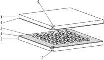
一种基于3D打印技术的柔性压力传感器芯片,包括柔性上极板1,柔性上极板1和均匀分布微型金字塔阵列3的柔性下极板2相接触,在柔性上极板1和柔性下极板2接触表面制作柔性薄膜电极4,柔性上极板1上的柔性薄膜电极4和柔性下极板2上的柔性薄膜电极4通过导线与外部电路相连接,导线位于柔性上极板1和柔性下极板2对应的角上设有的通孔5内。A flexible pressure sensor chip based on 3D printing technology, including a flexible
所述的柔性上极板1和柔性下极板2由光敏柔性聚氨酯树脂材料制成。The flexible
所述的柔性薄膜电极4由柔性导电聚合物PEDOT:PSS[聚(3,4-亚乙二氧基噻吩)-聚(苯乙烯磺酸)]制成。The flexible
一种基于3D打印技术的柔性压力传感器芯片的制作方法,包括以下步骤:A manufacturing method of a flexible pressure sensor chip based on 3D printing technology, comprising the following steps:
1)运用DLP 3D打印机固化处于液态的光敏柔性聚氨酯树脂材料形成预定尺寸的柔性上极板1和均匀分布微型金字塔阵列3的柔性下极板2,柔性上极板1、柔性下极板2对应的角上预留通孔5;1) Use a DLP 3D printer to cure the photosensitive flexible polyurethane resin material in liquid state to form a flexible
2)加工好的柔性上极板1和柔性下极板2依次置于清洗液、酒精中各超声清洗处理5min;取出柔性上极板1和柔性下极板2后置于紫外灯箱中20min使其完全固化;2) The processed flexible
3)将两根导线分别穿过柔性上极板1和柔性下极板2上预留的通孔5,并采用导电胶将导线紧密的黏附在柔性上极板1、柔性下极板2上,置于强制对流烘箱中,100℃烘烤10分钟使导电胶完全固化,取出后自然冷却至室温;3) Pass the two wires through the through
4)将与导线相连接的柔性上极板1、柔性下极板2置于等离子处理机中进行氧等离子体处理,处理时间90s;4) Place the flexible
5)将经过氧等离子体处理的柔性上极板1、柔性下极板2置于液态导电聚合物溶液PEDOT:PSS中,使柔性上极板1、柔性下极板2表面完全浸润一层PEDOT:PSS溶液;5) Place the flexible
6)取出表面浸润了PEDOT:PSS溶液的柔性上极板1、柔性下极板2,置于强制对流烘箱中,100℃烘烤15min,取出后自然冷却至室温,完成柔性薄膜电极4的制作;6) Take out the flexible
7)使用聚酰亚胺绝缘胶带将柔性上极板1、柔性下极板2粘贴在一起,同时封闭柔性上极板1、柔性下极板2侧面间隙。7) Use polyimide insulating tape to stick the flexible
本发明的有益效果为:The beneficial effects of the present invention are:
采用3D打印工艺(光固化成型)为制作方法,将柔性压阻材料PEDOT:PSS和柔性树脂相结合,拓展了传统传感器的材料选择范围。采用的光固化成型的3D打印工艺,具有较高的精度,可以制作复杂形状的微型结构,具有加工成本低、加工周期短、制作简便、材料选择多样化、结构一体化等优点。本发明的力传感器可应用在压力测量领域。Using 3D printing process (light curing molding) as the manufacturing method, the flexible piezoresistive material PEDOT:PSS and flexible resin are combined to expand the material selection range of traditional sensors. The photo-curing 3D printing process adopted has high precision and can produce micro-structures with complex shapes. It has the advantages of low processing cost, short processing cycle, simple production, diversified material selection, and structural integration. The force sensor of the present invention can be applied in the field of pressure measurement.
附图说明Description of drawings
图1为本发明柔性压力传感器芯片的结构示意图。FIG. 1 is a schematic structural diagram of a flexible pressure sensor chip of the present invention.
图2为本发明柔性压力传感器芯片的截面电阻模型示意图。FIG. 2 is a schematic diagram of a cross-sectional resistance model of the flexible pressure sensor chip of the present invention.
图3为本发明柔性压力传感器芯片的一种惠斯通测量电桥示意图。FIG. 3 is a schematic diagram of a Wheatstone measurement bridge of the flexible pressure sensor chip of the present invention.
具体实施方式Detailed ways
下面结合附图对本发明做详细描述。The present invention will be described in detail below with reference to the accompanying drawings.
如图1和图2所示,一种基于3D打印技术的柔性压力传感器芯片,包括柔性上极板1,柔性上极板1和均匀分布微型金字塔阵列3的柔性下极板2相接触,在柔性上极板1和柔性下极板2接触表面制作柔性薄膜电极4,柔性上极板1上的柔性薄膜电极4和柔性下极板2上的柔性薄膜电极4通过导线与外部电路连接,导线位于柔性上极板1和柔性下极板2对应的角上设有的通孔5内。As shown in Figures 1 and 2, a flexible pressure sensor chip based on 3D printing technology includes a flexible
所述的柔性上极板1和柔性下极板2由光敏柔性聚氨酯树脂材料制成。The flexible
所述的柔性薄膜电极4由柔性导电聚合物PEDOT:PSS[聚(3,4-亚乙二氧基噻吩)-聚(苯乙烯磺酸)]制成。The flexible
一种基于3D打印技术的柔性压力传感器芯片的制作方法,包括以下步骤:A manufacturing method of a flexible pressure sensor chip based on 3D printing technology, comprising the following steps:
1)运用DLP 3D打印机固化处于液态的光敏柔性聚氨酯树脂材料形成预定尺寸的柔性上极板1和均匀分布微型金字塔阵列3的柔性下极板2,柔性上极板1、柔性下极板2对应的角上预留通孔5;1) Use a DLP 3D printer to cure the photosensitive flexible polyurethane resin material in liquid state to form a flexible
2)加工好的柔性上极板1和柔性下极板2依次置于清洗液、酒精中各超声清洗处理5min以去除表面杂质及污染物;取出柔性上极板1和柔性下极板2后置于紫外灯箱中20min使其完全固化;2) The processed flexible
3)将两根导线分别穿过柔性上极板1和柔性下极板2上预留的通孔5,并采用导电胶将导线紧密的黏附在柔性上极板1、柔性下极板2上,置于强制对流烘箱中,100℃烘烤10分钟使导电胶完全固化,取出后自然冷却至室温;3) Pass the two wires through the through
4)将与导线相连接的柔性上极板1、柔性下极板2置于等离子处理机中进行氧等离子体处理,处理时间90s,增加柔性上极板1、柔性下极板2的亲水性,更加容易浸润液体;4) Place the flexible
5)将经过氧等离子体处理的柔性上极板1、柔性下极板2置于液态导电聚合物溶液PEDOT:PSS中30s,使柔性上极板1、柔性下极板2表面完全浸润一层PEDOT:PSS溶液,尽量保证浸润的均匀度与一致性;5) Place the flexible
6)取出表面浸润了PEDOT:PSS溶液的柔性上极板1、柔性下极板2,置于强制对流烘箱中,100℃烘烤15min,取出后自然冷却至室温,完成柔性薄膜电极4的制作;6) Take out the flexible
7)使用聚酰亚胺绝缘胶带将柔性上极板1、柔性下极板2粘贴在一起,同时封闭柔性上极板1、柔性下极板2侧面间隙,避免柔性薄膜电极4受空气湿度影响其压阻特性稳定性。7) Use polyimide insulating tape to stick the flexible
本发明柔性力传感器芯片的工作原理为:The working principle of the flexible force sensor chip of the present invention is as follows:
如图2所示,一个微型金字塔处的电阻模型,当某一均布载荷F作用于传感器柔性上极板1上表面时,微型金字塔阵列3受压力作用产生形变,从而改变柔性上极板1、柔性下极板2表面的柔性薄膜电极4的接触面积,即柔性上极板1、柔性下极板2间的总电阻R发生变化,总电阻R由上极板电阻Rt,上下极板接触电阻Rc,以及下极板电阻Rb组成,即As shown in Figure 2, a resistance model at a micro pyramid, when a uniform load F acts on the upper surface of the flexible
R=Rt+Rc+RbR=Rt +Rc +Rb
当柔性上极板1、柔性下极板2间距发生变化时,When the distance between the flexible
ΔR=R-R0=(Rt+Rc+Rb)-(Rt0+Rc0+Rb0)ΔR=RR0 =(Rt +Rc +Rb )-(Rt0 +Rc0 +Rb0 )
由于柔性上极板1、柔性下极板2的电阻几乎不变,上式可近似为Since the resistances of the flexible
ΔR≈(Rc-Rc0)+(Rb-Rb0)ΔR≈(Rc -Rc0 )+(Rb -Rb0 )
根据电阻定律According to the law of resistance

其中ρ:导体材料的电阻率,L:导体的长度,S:导体的横截面积,where ρ: the resistivity of the conductor material, L: the length of the conductor, S: the cross-sectional area of the conductor,
电阻值的变化表达式如下:The expression for the change of resistance value is as follows:

其中ρc为柔性薄膜电极材料的电阻率,Ac为上下极板表面的柔性薄膜电极的接触面积,Lc为上下极板接触位置柔性薄膜电极的厚度,Db为柔性薄膜电极在微型金字塔侧面的厚度,Cb为上下极板表面的柔性薄膜电极接触面的周长,Lb为薄膜电极在微型金字塔侧面的长度。where ρc is the resistivity of the flexible thin film electrode material, Ac is the contact area of the flexible thin film electrode on the surface of the upper and lower electrode plates, Lc is the thickness of the flexible thin film electrode at the contact position of the upper and lower electrode plates, Db is the flexible thin film electrode in the micro pyramid The thickness of the side, Cb is the perimeter of the contact surface of the flexible thin film electrode on the surface of the upper and lower plates, and Lb is the length of the thin film electrode on the side of the micro pyramid.
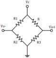
通过外接惠斯通电桥电路,如图3所示,其中R为待测压阻材料薄膜电阻,Vc为恒压源,R1,R2,R3为电桥电阻,Vo为输出电压,将这一阻值变化转变为电信号输出,从而实现传感器芯片的作用力—电信号转换,完成对作用力的测量。Through an external Wheatstone bridge circuit, as shown in Figure 3, where R is the film resistance of the piezoresistive material to be measured, Vc is a constant voltage source, R1, R2, and R3 are bridge resistances, and Vo is the output voltage. The value change is converted into an electrical signal output, so as to realize the force-electrical signal conversion of the sensor chip, and complete the measurement of the force.
Claims (1)
Translated fromChinesePriority Applications (1)
| Application Number | Priority Date | Filing Date | Title |
|---|---|---|---|
| CN201810349909.6ACN108515694B (en) | 2018-04-18 | 2018-04-18 | A flexible pressure sensor chip based on 3D printing technology and its manufacturing method |
Applications Claiming Priority (1)
| Application Number | Priority Date | Filing Date | Title |
|---|---|---|---|
| CN201810349909.6ACN108515694B (en) | 2018-04-18 | 2018-04-18 | A flexible pressure sensor chip based on 3D printing technology and its manufacturing method |
Publications (2)
| Publication Number | Publication Date |
|---|---|
| CN108515694A CN108515694A (en) | 2018-09-11 |
| CN108515694Btrue CN108515694B (en) | 2020-07-24 |
Family
ID=63429541
Family Applications (1)
| Application Number | Title | Priority Date | Filing Date |
|---|---|---|---|
| CN201810349909.6AActiveCN108515694B (en) | 2018-04-18 | 2018-04-18 | A flexible pressure sensor chip based on 3D printing technology and its manufacturing method |
Country Status (1)
| Country | Link |
|---|---|
| CN (1) | CN108515694B (en) |
Families Citing this family (10)
| Publication number | Priority date | Publication date | Assignee | Title |
|---|---|---|---|---|
| US20220034116A1 (en)* | 2018-09-28 | 2022-02-03 | General Electric Company | Method for manufacturing wind turbine tower structure with embedded reinforcement sensing elements |
| CN110440961B (en)* | 2019-08-16 | 2020-11-03 | 新昌县玮康电子科技有限公司 | Wearable piezoresistive sensor system and preparation process thereof |
| CN110608825B (en)* | 2019-09-12 | 2021-08-20 | 复旦大学 | Flexible pressure sensor based on polyimide substrate microstructure and preparation method thereof |
| CN111829697B (en)* | 2020-06-17 | 2022-07-05 | 华中科技大学 | A kind of flexible pressure sensor with convex hemispheric structure and preparation method thereof |
| CN112729628A (en)* | 2020-12-25 | 2021-04-30 | 吉林大学 | Hypersensitive flexible sensor and preparation method thereof |
| CN112895433B (en)* | 2021-01-14 | 2022-04-12 | 河北工业大学 | 3D printing-based flexible sensor device and preparation method thereof |
| CN112924060B (en)* | 2021-01-22 | 2022-09-30 | 宁波诺丁汉新材料研究院有限公司 | Flexible pressure sensor and preparation method thereof |
| CN215641015U (en)* | 2021-04-27 | 2022-01-25 | 杭州电子科技大学 | Magnetic sensing eddy current nondestructive flaw detection system |
| CN115742284B (en)* | 2022-11-01 | 2025-08-26 | 福建星海通信科技有限公司 | A method for preparing a flexible pressure sensor based on FDM 3D printing |
| CN118906460A (en)* | 2024-08-27 | 2024-11-08 | 上海爱特一信生物科技有限公司 | Post-curing method of 3D thin-wall shell-shaped product |
Citations (2)
| Publication number | Priority date | Publication date | Assignee | Title |
|---|---|---|---|---|
| CN104359597A (en)* | 2014-11-13 | 2015-02-18 | 中国科学院重庆绿色智能技术研究院 | Electronic skin based on three-dimensional flexible substrate graphene and preparing method thereof |
| CN104409172A (en)* | 2014-05-31 | 2015-03-11 | 福州大学 | 3D manufacturing method of latticed conducting array |
Family Cites Families (1)
| Publication number | Priority date | Publication date | Assignee | Title |
|---|---|---|---|---|
| CN105865667B (en)* | 2016-05-19 | 2018-06-01 | 北京印刷学院 | Capacitive flexible pressure sensor based on microstructured dielectric layer and its preparation method |
- 2018
- 2018-04-18CNCN201810349909.6Apatent/CN108515694B/enactiveActive
Patent Citations (2)
| Publication number | Priority date | Publication date | Assignee | Title |
|---|---|---|---|---|
| CN104409172A (en)* | 2014-05-31 | 2015-03-11 | 福州大学 | 3D manufacturing method of latticed conducting array |
| CN104359597A (en)* | 2014-11-13 | 2015-02-18 | 中国科学院重庆绿色智能技术研究院 | Electronic skin based on three-dimensional flexible substrate graphene and preparing method thereof |
Also Published As
| Publication number | Publication date |
|---|---|
| CN108515694A (en) | 2018-09-11 |
Similar Documents
| Publication | Publication Date | Title |
|---|---|---|
| CN108515694B (en) | A flexible pressure sensor chip based on 3D printing technology and its manufacturing method | |
| CN108731851B (en) | Flexible capacitive pressure sensor and preparation method thereof | |
| CN112556895B (en) | Flexible pressure sensor, preparation method, sensing system and flexible electronic skin | |
| CN110398259B (en) | Flexible sensor device with multi-sensing function and preparation method | |
| CN110375895B (en) | Multifunctional fully flexible fingerprint-shaped touch sensor | |
| CN108007617A (en) | Pressure resistance type flexible touch sensation sensor and its manufacture method with micro- frustum of a cone substrate | |
| CN113218542B (en) | High-sensitivity flexible three-dimensional force touch sensor and preparation method thereof | |
| CN110793701A (en) | A high-sensitivity capacitive flexible three-dimensional force tactile sensor and preparation method thereof | |
| CN105606270A (en) | Composite capacitor-resistor type full-flexibility touch and pressure sensor | |
| CN111829697B (en) | A kind of flexible pressure sensor with convex hemispheric structure and preparation method thereof | |
| CN108063183A (en) | A kind of method that closing porous piezoelectric electret energy accumulator is prepared based on nano impression | |
| CN113138042B (en) | A capacitive flexible pressure sensor with PDMS-PS polymer dielectric and its manufacturing process | |
| CN110426063A (en) | A kind of double mode sensor and its application in detection pressure and strain path | |
| CN114705334A (en) | Linear piezoresistive touch sensor and preparation method thereof | |
| CN112229546A (en) | A method for fabricating a flexible piezoelectric three-dimensional sensing array | |
| CN111786590A (en) | Triboelectric nanogenerator and flexible sensor that can simultaneously detect temperature and pressure | |
| CN107244070A (en) | A kind of sensor chip and its 3D printing preparation method based on electrically conductive ink | |
| CN113551811A (en) | A design method for a 4D printed multifunctional tactile sensor | |
| CN103759866B (en) | Coplanar small electrode type soft pressure sensitive probe and method of production thereof | |
| CN116715879A (en) | Microstructured elastomer film, preparation method and wearable flexible sensor | |
| CN115014596B (en) | A piezoresistive flexible tactile sensor and its manufacturing method | |
| CN211042262U (en) | Dual-mode sensor | |
| CN112729626B (en) | Linear capacitive touch sensor and preparation method thereof | |
| CN114993523B (en) | Variable-area capacitive pressure sensor with circular-convex structure and preparation method thereof | |
| CN112477112B (en) | A neural-like tactile sensor based on 4D printing |
Legal Events
| Date | Code | Title | Description |
|---|---|---|---|
| PB01 | Publication | ||
| PB01 | Publication | ||
| SE01 | Entry into force of request for substantive examination | ||
| SE01 | Entry into force of request for substantive examination | ||
| GR01 | Patent grant | ||
| GR01 | Patent grant | ||
| TR01 | Transfer of patent right | ||
| TR01 | Transfer of patent right | Effective date of registration:20201009 Address after:Room 10101, floor 1, building 1, East Industrial Building, modern enterprise center, No. 2, zhangbawu Road, hi tech Zone, Xi'an City, Shaanxi Province 710000 Patentee after:XI'AN WINWAY MACHINERY Co.,Ltd. Address before:Beilin District Xianning West Road 710049, Shaanxi city of Xi'an province No. 28 Patentee before:XI'AN JIAOTONG University |