CN108511440B - Semiconductor structure with capacitor connection pad and method of making capacitor connection pad - Google Patents
Semiconductor structure with capacitor connection pad and method of making capacitor connection padDownload PDFInfo
- Publication number
- CN108511440B CN108511440BCN201710102423.8ACN201710102423ACN108511440BCN 108511440 BCN108511440 BCN 108511440BCN 201710102423 ACN201710102423 ACN 201710102423ACN 108511440 BCN108511440 BCN 108511440B
- Authority
- CN
- China
- Prior art keywords
- top surface
- substrate
- capacitor
- bit line
- dielectric layer
- Prior art date
- Legal status (The legal status is an assumption and is not a legal conclusion. Google has not performed a legal analysis and makes no representation as to the accuracy of the status listed.)
- Active
Links
Images


Classifications
- H—ELECTRICITY
- H10—SEMICONDUCTOR DEVICES; ELECTRIC SOLID-STATE DEVICES NOT OTHERWISE PROVIDED FOR
- H10B—ELECTRONIC MEMORY DEVICES
- H10B12/00—Dynamic random access memory [DRAM] devices
- H10B12/30—DRAM devices comprising one-transistor - one-capacitor [1T-1C] memory cells
- H10B12/31—DRAM devices comprising one-transistor - one-capacitor [1T-1C] memory cells having a storage electrode stacked over the transistor
- H10B12/315—DRAM devices comprising one-transistor - one-capacitor [1T-1C] memory cells having a storage electrode stacked over the transistor with the capacitor higher than a bit line
- H—ELECTRICITY
- H01—ELECTRIC ELEMENTS
- H01L—SEMICONDUCTOR DEVICES NOT COVERED BY CLASS H10
- H01L21/00—Processes or apparatus adapted for the manufacture or treatment of semiconductor or solid state devices or of parts thereof
- H01L21/70—Manufacture or treatment of devices consisting of a plurality of solid state components formed in or on a common substrate or of parts thereof; Manufacture of integrated circuit devices or of parts thereof
- H01L21/71—Manufacture of specific parts of devices defined in group H01L21/70
- H01L21/768—Applying interconnections to be used for carrying current between separate components within a device comprising conductors and dielectrics
- H01L21/76801—Applying interconnections to be used for carrying current between separate components within a device comprising conductors and dielectrics characterised by the formation and the after-treatment of the dielectrics, e.g. smoothing
- H01L21/76802—Applying interconnections to be used for carrying current between separate components within a device comprising conductors and dielectrics characterised by the formation and the after-treatment of the dielectrics, e.g. smoothing by forming openings in dielectrics
- H01L21/76816—Aspects relating to the layout of the pattern or to the size of vias or trenches
- H—ELECTRICITY
- H10—SEMICONDUCTOR DEVICES; ELECTRIC SOLID-STATE DEVICES NOT OTHERWISE PROVIDED FOR
- H10B—ELECTRONIC MEMORY DEVICES
- H10B12/00—Dynamic random access memory [DRAM] devices
- H10B12/01—Manufacture or treatment
- H—ELECTRICITY
- H10—SEMICONDUCTOR DEVICES; ELECTRIC SOLID-STATE DEVICES NOT OTHERWISE PROVIDED FOR
- H10B—ELECTRONIC MEMORY DEVICES
- H10B12/00—Dynamic random access memory [DRAM] devices
- H10B12/01—Manufacture or treatment
- H10B12/02—Manufacture or treatment for one transistor one-capacitor [1T-1C] memory cells
- H10B12/03—Making the capacitor or connections thereto
- H10B12/033—Making the capacitor or connections thereto the capacitor extending over the transistor
- H10B12/0335—Making a connection between the transistor and the capacitor, e.g. plug
- H—ELECTRICITY
- H10—SEMICONDUCTOR DEVICES; ELECTRIC SOLID-STATE DEVICES NOT OTHERWISE PROVIDED FOR
- H10B—ELECTRONIC MEMORY DEVICES
- H10B12/00—Dynamic random access memory [DRAM] devices
- H10B12/30—DRAM devices comprising one-transistor - one-capacitor [1T-1C] memory cells
- H10B12/34—DRAM devices comprising one-transistor - one-capacitor [1T-1C] memory cells the transistor being at least partially in a trench in the substrate
Landscapes
- Engineering & Computer Science (AREA)
- Manufacturing & Machinery (AREA)
- Physics & Mathematics (AREA)
- Condensed Matter Physics & Semiconductors (AREA)
- General Physics & Mathematics (AREA)
- Computer Hardware Design (AREA)
- Microelectronics & Electronic Packaging (AREA)
- Power Engineering (AREA)
- Internal Circuitry In Semiconductor Integrated Circuit Devices (AREA)
- Semiconductor Memories (AREA)
Abstract
Translated fromChinese
Description
Translated fromChinese技术领域technical field
本发明涉及一种电容连接垫的制作方法,特别是涉及一种围绕电容连接垫的介电层其底面低于位线的顶面的制作方法。The present invention relates to a method for manufacturing a capacitor connection pad, in particular to a method for manufacturing a dielectric layer surrounding the capacitor connection pad whose bottom surface is lower than the top surface of a bit line.
背景技术Background technique
动态随机存取存储器(dynamic random access memory,DRAM)是由数目庞大的存储单元(memory cell)所聚集而成的。DRAM中的每一个存储单元包含有一个晶体管作为一开关晶体管以及一个电容用来存储电荷。电容是通过下电极与电容连接垫(landing pad)电连接,电容连接垫与电容接触插塞电连接,并与晶体管的漏极形成存取的通路。Dynamic random access memory (dynamic random access memory, DRAM) is composed of a large number of memory cells (memory cells). Each memory cell in DRAM includes a transistor as a switching transistor and a capacitor for storing charge. The capacitor is electrically connected to a capacitor connecting pad (landing pad) through the lower electrode, and the capacitor connecting pad is electrically connected to the capacitor contact plug, and forms an access path with the drain of the transistor.
随着DRAM上的集成度快速增加,电容连接垫的尺寸也越来越小,因此利用曝光步骤定义电容连接垫的位置时,常会发生对不准的情况,导致之后在形成电容连接垫时,发生相邻的电容连接垫依然彼此连接的情况,如此会造成电路短路的现象。With the rapid increase of the integration level on DRAM, the size of the capacitor connection pad is getting smaller and smaller. Therefore, when using the exposure step to define the position of the capacitor connection pad, misalignment often occurs, resulting in the subsequent formation of the capacitor connection pad. It occurs that the adjacent capacitor connection pads are still connected to each other, which may cause a short circuit phenomenon.
发明内容SUMMARY OF THE INVENTION
有鉴于此,本发明提供一种电容连接垫的制作方法,以解决上述问题。In view of this, the present invention provides a manufacturing method of a capacitor connection pad to solve the above problems.
根据本发明的第一优选实施例,一种具有电容连接垫的半导体结构,包含一基底,一电容接触插塞设置于基底上,一电容连接垫接触并连结电容接触插塞,一位线设置于基底上以及一介电层围绕电容连接垫,介电层具有一底面低于位线的一顶面。According to a first preferred embodiment of the present invention, a semiconductor structure having a capacitor connection pad includes a substrate, a capacitor contact plug is disposed on the substrate, a capacitor connection pad contacts and is connected to the capacitor contact plug, and a bit line is disposed The capacitor connection pad is surrounded by a dielectric layer on the substrate, and the dielectric layer has a bottom surface lower than a top surface of the bit line.
根据本发明的第二优选实施例,一种电容连接垫的制作方法,一种电容连接垫的制作方法,包含:提供一基底,多个字符线埋入于基底中,各个字符线正上方各自设置有一绝缘层,相邻的各个绝缘层之间定义出一开口,然后形成一金属层填入开口,并且使得各个绝缘层完全埋入于金属层中,接着形成一第一硬掩模覆盖金属层,之后进行一第一图案化制作工艺,图案化第一硬掩模,使得第一硬掩模转变为多个第二硬掩模,接续进行一第二图案化制作工艺,图案化各个第二硬掩模,使得第二硬掩模转变为多个第三硬掩模,其中各个第三硬掩模不相连并且各个第三硬掩模分别部分重叠绝缘层的其中之一,然后以全部的第三硬掩模为掩模移除金属层以在金属层上形成一沟槽,沟槽延伸至开口中并且沟槽的一底面低于绝缘层的一顶面,其中沟槽于金属层上定义出多个电容连接垫,最后形成一介电层填满沟槽。According to a second preferred embodiment of the present invention, a method for fabricating a capacitor connection pad, and a method for fabricating a capacitor connection pad, include: providing a substrate, a plurality of character lines are embedded in the substrate, and each character line is directly above the An insulating layer is provided, an opening is defined between adjacent insulating layers, and then a metal layer is formed to fill the opening, and each insulating layer is completely buried in the metal layer, and then a first hard mask is formed to cover the metal layer, and then perform a first patterning process to pattern the first hard mask so that the first hard mask is transformed into a plurality of second hard masks, and then perform a second patterning process to pattern each of the first hard masks. Two hard masks, so that the second hard mask is transformed into a plurality of third hard masks, wherein the third hard masks are not connected and the third hard masks respectively partially overlap one of the insulating layers, and then all the third hard masks are The third hard mask is a mask to remove the metal layer to form a trench in the metal layer, the trench extends into the opening and a bottom surface of the trench is lower than a top surface of the insulating layer, wherein the trench is in the metal layer A plurality of capacitor connection pads are defined above, and finally a dielectric layer is formed to fill the trenches.
根据本发明的第三优选实施例一种接触结构,用于电连接动态随机存取存储器单元中的电容与晶体管,包含:一电容连接垫和电容接触插塞。电容连接垫包含一第一部件和一第二部件。According to a third preferred embodiment of the present invention, a contact structure for electrically connecting a capacitor and a transistor in a dynamic random access memory cell includes: a capacitor connection pad and a capacitor contact plug. The capacitive connection pad includes a first part and a second part.
第一部件包含一第一底面,第二部件包含一第一顶面和一第二底面,其中第一底面接触第一顶面,第一底面的面积小于第一顶面的面积,此外第二部件位于第一部件和电容接触插塞之间,电容接触插塞包含一第二顶面,第二顶面接触第二底面,第二顶面的面积小于第二底面的面积。The first part includes a first bottom surface, the second part includes a first top surface and a second bottom surface, wherein the first bottom surface contacts the first top surface, the area of the first bottom surface is smaller than that of the first top surface, and the second The component is located between the first component and the capacitive contact plug, the capacitive contact plug includes a second top surface, the second top surface contacts the second bottom surface, and the area of the second top surface is smaller than that of the second bottom surface.
附图说明Description of drawings
图1至图12为本发明的一优选实施例所绘示的电容连接垫的制作方法的示意图,其中:1 to 12 are schematic diagrams illustrating a method for fabricating a capacitor connection pad according to a preferred embodiment of the present invention, wherein:
图1为提供基底和形成金属层的制作工艺示意图;1 is a schematic diagram of a fabrication process for providing a substrate and forming a metal layer;
图2为接续图1的制作工艺示意图;Fig. 2 is the production process schematic diagram of continuation of Fig. 1;
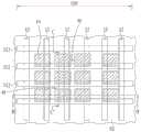
图3为图2的存储器区的上视图;Fig. 3 is the top view of the memory area of Fig. 2;
图4为接续图2的制作工艺示意图;Fig. 4 is the production process schematic diagram of continuation of Fig. 2;
图5为接续图4的制作工艺示意图;FIG. 5 is a schematic diagram of the manufacturing process following FIG. 4;
图6为图5中存储器区的上视图;Fig. 6 is the top view of the memory area in Fig. 5;
图7为接续图5的制作工艺示意图;FIG. 7 is a schematic diagram of the manufacturing process following FIG. 5;
图8为接续图7中存储器区的制作工艺步骤的上视图;FIG. 8 is a top view of the manufacturing process steps of the memory area in succession in FIG. 7;
图9为图8中沿着AA’切线所绘示的侧示图;Figure 9 is a side view drawn along the AA' tangent in Figure 8;
图10为接续图8的制作工艺步骤的上视图;FIG. 10 is a top view of the manufacturing process step following FIG. 8;
图11为图10中沿着BB’切线所绘示的侧示图;Figure 11 is a side view drawn along the BB' tangent in Figure 10;
图12为图10中沿着CC’切线所绘示的侧示图;Figure 12 is a side view drawn along the tangent line CC' in Figure 10;
图13至图18为本发明的一优选实施例所绘示的用于电连接动态随机存取存储器单元中的电容与晶体管的接触结构的制作方法的示意图,其中:13 to 18 are schematic diagrams of a method for fabricating a contact structure for electrically connecting a capacitor and a transistor in a DRAM cell according to a preferred embodiment of the present invention, wherein:
图13为提供基底、形成接触插塞的制作工艺示意图;13 is a schematic diagram of a manufacturing process for providing a substrate and forming a contact plug;
图14为接续图13的制作工艺示意图;FIG. 14 is a schematic diagram of the manufacturing process following FIG. 13;
图15为接续图14的制作工艺示意图;FIG. 15 is a schematic diagram of the manufacturing process following FIG. 14;
图16为接续图15的制作工艺示意图;FIG. 16 is a schematic diagram of the manufacturing process following FIG. 15;
图17为接续图16的制作工艺示意图;FIG. 17 is a schematic diagram of the manufacturing process following FIG. 16;
图18为接续图17的制作工艺示意图;FIG. 18 is a schematic diagram of the manufacturing process following FIG. 17;
图19A为图18中的接触结构的立体图;FIG. 19A is a perspective view of the contact structure in FIG. 18;
图19B为接触结构的立体图的变化型;19B is a modification of the perspective view of the contact structure;
图20为图19A的立体分解图。Fig. 20 is an exploded perspective view of Fig. 19A.
主要元件符号说明Description of main component symbols
10 基底 11 浅沟槽绝缘10
12 字符线 16 绝缘层12
18 字符线掩模 20 层间介电层18 Wordline
22 沟槽 24 导电层22
26 外延层 28 晶体管26
30 介电层 32 源极漏极掺杂区30
34 沟槽 35 沟槽34 Groove 35 Groove
36 金属层 38 第一硬掩模36
40 第一光致抗蚀剂 42 有机介电层40
43 第一矩形图案 44 含硅底部抗反射层43 first
46 第二矩形图案 48 沟槽46 Second
50 底面 52 顶面50 Bottom 52 Top
54 电容连接垫 56 电容接触插塞54
58 源极漏极导电垫 60 栅极连接垫58 Source-drain
62 介电层 64 底面62
66 顶面 68 顶面66 Top 68 Top
70 上表面 72 位线掩模70
100 存储器区 112 位线100 memory banks 112-bit lines
138 第二硬掩模 142 有机介电层138 Second
144 含硅底部抗反射层 200 周边电路区144 Silicon-containing bottom
238 第三硬掩模 240 第二光致抗蚀剂238 Third
300 基底 311 浅沟槽绝缘300
312 字符线 313 源极漏极掺杂区312
314 晶体管 316 第一层间介电层314
318 接触洞 320 电容接触插塞318
322 上表面 324 上表面322
326 第二介电层材料 328 光掩模326 Second
330 预定图案 332 图案化光致抗蚀剂330
334 侧壁 336 侧壁334
338 开口 340 孔洞338
342 初步的电容连接垫 344 上表面342 Preliminary
346 上表面 348 侧壁346
350 图案化光致抗蚀剂 352 开口350
354 孔洞 356 电容连接垫354
358 接触结构 360 介电层358
362 上表面 366 电容362
368 第一部件 370 第二部件368
372 第一底面 374 第一顶面372 First
376 第二底面 378 第二顶面376
具体实施方式Detailed ways
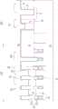
如图1所示,首先提供一基底10,基底10中设置有一存储器区100,在存储器区100中,设置有多个主动区域(图未示)和多个浅沟槽隔离11,多个字符线12埋入于基底10中,并且其中几条字符线12会通过浅沟槽隔离11,多个位线(图未示)设置于基底10上,并且各个位线和各个字符线12交错,此外,在各个字符线12的正上方设置有绝缘层16,绝缘层16可以包含字符线掩模18和层间介电层20,绝缘层16可以为单层或多层材料,绝缘层16的材料可以选自氧化硅、氮化硅或氮氧化硅等,在相邻的各个绝缘层16之间定义出一开口22,在各个绝缘层16上和开口22内可以顺应地形成一导电层24。在各个相邻的字符线12之间的基底10上可以选择性地设置有一外延层26,在外延层26下方的基底10中可以设置有掺杂区(图未示),在本实施例中,开口22会在外延层26的正上方。基底10可以另外包含一周边电路区200,周边电路区200内可以设置有一晶体管28,例如一平面式晶体管,晶体管28的栅极上方设置有一开口35,在周边电路区200设置有一介电层30覆盖基底10,在源极漏极掺杂区32上方另设置有一开口34位于介电层30中,导电层24亦覆盖开口34内侧。As shown in FIG. 1 , a
接着形成一金属层36填入各个开口22、开口34和开口35,并且使得所有的绝缘层16完全埋入于金属层36中,并且金属层36的上表面较绝缘层16的顶面52高,之后形成一第一硬掩模38覆盖金属层36。Next, a
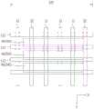
如图2所示,接着进行一第一图案化制作工艺,先全面形成一第一光致抗蚀剂40覆盖第一硬掩模38,第一光致抗蚀剂40和第一硬掩模38之间可以另外由下至上依序形成一有机介电层(organic dielectric layer,ODL)42和一含硅底部抗反射层(silicon-containing hard mask bottom anti-reflection coating,SHB)44。然后图案化第一光致抗蚀剂40,请同时参阅图2和图3,图3为图2中的存储器区100的上视图,为了图示简单明了,在图3只绘示出字符线、位线和图案化后的第一光致抗蚀剂。如图2和图3所示,多条字符线12和多条位线112交错,图案化后的第一光致抗蚀剂40包含至少一第一矩形图案43,在本实例中以多个第一矩形图案43为例,各第一矩形图案43和各字符线12平行,值得注意的是由于在曝光的过程光掩模发生偏移,在本实施例中光掩模朝向水平方向X偏移,水平方向X和位线112平行,因此在存储器区100中,各个第一矩形图案43同时覆盖一个相对应的开口22以及与此开口22相邻的绝缘层16。视光掩模的偏移程度,第一矩形图案43可能会覆盖部分的开口22以及完全覆盖与开口22相邻的绝缘层16,但在不同的实施例中,当在第一矩形图案43的大小不变的情况下发生偏移时,第一矩形图案43也有可能只部分覆盖绝缘层16,但覆盖较多的开口22。此外,由于光掩模的偏移方向是随机的,所以光掩模也有可能朝向垂直方向Y偏移,垂直方向Y和字符线12平行,又或者光掩模也可能正确的对准没有偏移发生。As shown in FIG. 2 , a first patterning process is then performed, and a
如图4所示,先将各个第一矩形图案43转印至含硅底部抗反射层44和有机介电层42上,然后移除第一光致抗蚀剂40,接着将含硅底部抗反射层44和有机介电层42的图案转印至第一硬掩模38,使第一硬掩模38变成多个第二硬掩模138,接着移除含硅底部抗反射层44和有机介电层42,各个第二硬掩模138为矩形图案,各第二硬掩模138各自对应一个第一矩形图案43的位置,因此在存储器区100中各个第二硬掩模138各自同时覆盖一个开口22以及与开口22相邻的绝缘层16,在本实施中,各个第二硬掩模138同时覆盖部分的开口22以及完全覆盖与开口22相邻的绝缘层16。As shown in FIG. 4 , each first
如图5所示,接着进行一第二图案化制作工艺,全面形成一第二光致抗蚀剂240覆盖第二硬掩模138,第二光致抗蚀剂240和第二硬掩模138之间可以另外由下至上依序形成一有机介电层142和一含硅底部抗反射层144。请同时参阅图5和图6,图6为图5中存储器区的上视图,为了图示简单明了,在图6只绘示出字符线、位线和图案化后的第二光致抗蚀剂。如图5所示,图案化后的第二光致抗蚀剂240包含至少一第二矩形图案46,在本实例中以多个第二矩形图案46为例,各第二矩形图案46和各位线112平行,同样地,由于在曝光的过程中光掩模可能发生偏移,并且光掩模的偏移方向是随机的,所以光掩模有可能朝向垂直方向Y偏移,或是朝向水平方向X偏移,又或者光掩模可能正确的对准没有偏移发生。在本实施例中光掩模向垂直方向Y偏移。此外请同时参阅图3和图6,各第二矩形图案46和各第一矩形图案43交错,在每一第二矩形图案46和每一第一矩形图案43重叠的位置所对应的金属层36即是之后各电容连接垫所在的位置。As shown in FIG. 5 , a second patterning process is then performed to form a
如图7所示,先将各个第二矩形图案46转印至含硅底部抗反射层144和有机介电层142上,然后移除第二光致抗蚀剂240,接着将含硅底部抗反射层144和有机介电层142上的图案转印至第二硬掩模138,使每一个第二硬掩模138与各个第二矩形图案46重叠的位置分别被保留下来,而变成多个第三硬掩模238。接着移除含硅底部抗反射层144和有机介电层142,此时在存储器区100内,该些第三硬掩模238即定义出之后各电容连接垫所在的位置,各个第三硬掩模238不相连,并且各个第三硬掩模238分别各自重叠一个绝缘层16,在本实施例中一个第三硬掩模238部分重叠一个开口22并且完全重叠一个绝缘层16。As shown in FIG. 7 , each second
图8为接续图7的制作工艺步骤的上视图,图9为图8中沿着AA’切线所绘示的侧示图,其中为了图示简单明了,在图8只绘示存储器区中字符线、位线和电容连接垫。请同时参阅图8和图9,以第三硬掩模238为掩模移除金属层36以在金属层36上形成至少一沟槽48,沟槽48延伸至开口22中并且沟槽48的一底面50低于绝缘层16的顶面52。之后移除第三硬掩模238。FIG. 8 is a top view following the manufacturing process steps of FIG. 7 , and FIG. 9 is a side view taken along the tangent line AA′ in FIG. 8 . For the sake of simplicity and clarity, only characters in the memory area are shown in FIG. 8 . lines, bit lines and capacitor connection pads. Referring to FIGS. 8 and 9 at the same time, the
在另一实施例中,若是在第三硬掩模238只部分重叠一个绝缘层16的情况下,部分的绝缘层16也会被移除,移除的绝缘层16所形成的空间则成为沟槽48的一部分。在本实施例中以在第三硬掩模238完全重叠一个绝缘层16为例。在移除部分的金属层36后,在绝缘层16的顶面52之上的剩余的金属层36就作为电容连接垫54,换而言之沟槽48在金属层36上定义出电容连接垫54的位置,电容连接垫54在图示中以右上至左下的斜线标示,而在开口22中并且位于绝缘层16的顶面52之下的金属层36则作为电容接触插塞56。如上文所述,由于在光掩模对准时常会发生偏移的现象,因此本发明特意使得沟槽48的底面50低于绝缘层16的顶面52,以确保相邻的电容连接垫54彼此不接触。另外,沟槽48在存储器区100内交错形成一棋盘图案,并且沟槽48平行于位线112和字符线12,沟槽48亦垂直于位线112和字符线12。另外,在周边电路区200中,剩余的金属层36作为一源极漏极导电垫58以及一栅极连接垫60。In another embodiment, if the third
图10为接续图8的制作工艺步骤的上视图,图11为图10中沿着BB’切线所绘示的侧示图,图12为图10中沿着CC’切线所绘示的侧示图,其中为了图示简单明了,在图10只绘示出存储器区内的字符线、位线、电容连接垫以及介电层。请同时参阅图10和图11,全面形成一介电层62在基底10上,在存储器区100内的介电层62构成一棋盘图案,并且介电层62填入电容连接垫54之间的沟槽48,之后可以在电容连接垫54上形成一电容(图未示),此时字符线12所构成的晶体管和电容就可形成一动态随机存取存储器单元。值得注意的是介电层62的底面64会比绝缘层16的顶面52低。此外,如图12所示,本发明的介电层62的底面64低于位线112的一顶面66,如此可以降低寄生电容。FIG. 10 is a top view following the manufacturing process steps in FIG. 8 , FIG. 11 is a side view along the tangent line BB′ in FIG. 10 , and FIG. 12 is a side view along the tangent line CC′ in FIG. 10 . In the drawings, for the sake of simplicity and clarity, only word lines, bit lines, capacitor connection pads and dielectric layers in the memory region are shown in FIG. 10 . Please refer to FIG. 10 and FIG. 11 at the same time, a
请同时参阅图10和图12,根据本发明的一优选实施例,一种具有电容连接垫的半导体结构,包含一基底10,至少一电容接触插塞56设置于基底10上,在图12中以多个电容接触插塞56为例,一电容连接垫54各别接触并连结一个电容接触插塞56,电容连接垫54和电容接触插塞56形成一阶梯结构,一位线112设置于基底10上,一介电层62围绕各电容连接垫54,介电层62具有一底面64低于位线112的一顶面66,此外,电容连接垫54的一顶面68和基底10的一上表面70之间设置有一第一距离D1,位线112的顶面66和基底10的上表面70之间设置有一第二距离D2,第一距离D1大于第二距离D2。一位线掩模72覆盖位线112,位线112的顶面66接触位线掩模72,并且位线掩模72位于电容连接垫54和位线112之间,位线112的顶面66接触位线掩模72。另外电容连接垫54是位于位线掩模72之上,而电容接触插塞56是位于位线掩模72之下。Please refer to FIG. 10 and FIG. 12 at the same time. According to a preferred embodiment of the present invention, a semiconductor structure with capacitive connection pads includes a
本发明特别让围绕电容连接垫的介电层的底面低于位线的顶面,以降低寄生电容,并且确保各个电容连接垫能够彼此绝缘。The present invention specifically makes the bottom surface of the dielectric layer surrounding the capacitive connection pads lower than the top surface of the bit line to reduce parasitic capacitance and ensure that the individual capacitive connection pads can be insulated from each other.
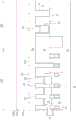
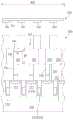
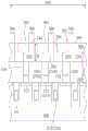
图13至图18为依据本发明的另一较佳实施例所绘示的用于电连接动态随机存取存储器单元中的电容与晶体管的接触结构的制作方法。图13所示,首先提供一基底300,基底300中设置有一存储器区400,在存储器区400中,设置有多个主动区域(图未示)和多个浅沟槽隔离311,多个字符线312埋入于基底300中,并且其中几条字符线312会通过浅沟槽隔离311,多个位线(图未示)设置于基底300上,并且各个位线和各个字符线312交错。此外在相邻字符线312之间各别设置有一源极漏极掺杂区313,源极漏极掺杂区313和其相邻的字符线312构成一晶体管314,接着在基底300上形成一第一层间介电层316覆盖基底300,然后在第一层间介电层316中形成多个接触洞318,由各个接触洞318曝露出源极漏极掺杂区313,之后再形成导电材料填入各个接触洞318,填入接触洞318的导电材料则作为电容接触插塞320,电容接触插塞320经由源极漏极掺杂区313电连结晶体管314,再者电容接触插塞320的上表面322和第一介电层316的上表面324切齐,导电材料可以为单层或是多层材料,导电材料可以包含掺杂多晶硅、钴硅化物、钨、铜或铝等导电材料,在本发明中,导电材料包含掺杂多晶硅、钴硅化物和钨由下至上堆叠。13 to 18 illustrate a method for fabricating a contact structure for electrically connecting a capacitor and a transistor in a dynamic random access memory cell according to another preferred embodiment of the present invention. As shown in FIG. 13 , a
如图14所示,形成一第二介电层材料326覆盖第一介电层316。然后在第二介电层326上形成一光致抗蚀剂,之后提供一光掩模328,光掩模328上包含多个预定图案330,预定图案330是用于定义初步的电容连接垫的位置,配合曝光显影制作工艺后此预定图案330将会转印到光致抗蚀剂上,使光致抗蚀剂形成一图案化光致抗蚀剂332,图案化光致抗蚀剂332在第二介电层326上定义出初步的电容连接垫的位置,在此步骤中,会特意调整光掩模328的位置,使得预定图案330的一侧壁334对齐电容接触插塞320的一侧壁336。此外以本实施例来说,图案化光致抗蚀剂332上包含多个开口338,开口338曝露出来的第二介电层326在后续将会被初步的电容连接垫取代,而初步的电容连接垫在之后经过修整后会成为本发明的电容连接垫。As shown in FIG. 14 , a second
请同时参阅图14和图15,以图案化光致抗蚀剂332为掩模蚀刻第二介电层326,在第二介电层326中形成多个孔洞340,然后移除图案化光致抗蚀剂332,接续形成一导电材料填入各个孔洞340,填入各孔洞340的导电材料作为初步的电容连接垫342,导电材料优选为钨,当然其它适合的导电材料也都可以作为初步的电容连接垫342。此外初步的电容连接垫342的上表面344和第二介电层326的上表面346切齐。值得注意的是初步的电容连接垫342的一侧壁348和电容接触插塞320的侧壁336切齐。各个初步的电容连接垫342包含一高度H,此高度H也就等于侧壁348的长度。14 and 15, the
根据本发明的另一优选实施例,电容接触插塞320和初步的电容连接垫342可以同时形成,举例而言,如图13中所描述的先在第一介电层316中形成多个接触洞318,但接续先不填入导电材料,反而先进行图14和图15中形成图案化光致抗蚀剂332以及形成多个孔洞340的步骤,然后形成导电材料同时填入各个接触洞336和各个孔洞340,同步形成电容接触插塞320和初步的电容连接垫342。如图16所示,在完成电容接触插塞320和初步的电容连接垫342之后,形成另一光致抗蚀剂覆盖第二介电层326,利用光掩模328配合曝光显影制作工艺,图案化光致抗蚀剂以形成一图案化光致抗蚀剂350,值得注意的是在本步骤使用的光掩模328和在图14中所用的光掩模328是同一个,其不同之处在于在本步骤中的预定图案330其目的在于定义出初步的电容连接垫342欲修整的位置,因此预定图案330会部分重叠初步的电容连接垫342并且预定图案330的侧壁334不会和电容接触插塞320的侧壁336对齐,而在图14中的预定图案330其目的在于定义出初步的电容连接垫342本身的位置。图案化光致抗蚀剂350包含多个开口352,一个开口352对应一个初步的电容连接垫342,每个初步电容连接垫342有部分由其所对应的开口352曝露出来,详细来说,各个初步的电容连接垫342的截面包含一宽度W,由侧壁348起算至少三分之一至三分之二的宽度W由开口352曝露出来,此外部分的第二介电层326也从各个开口352曝露出来。在本实施例中以由侧壁348起算二分一的宽度W由开口352曝露出来为例。According to another preferred embodiment of the present invention, the capacitive contact plugs 320 and the preliminary
请同时参阅图16和图17,以图案化光致抗蚀剂350为掩模移除曝露出来的初步的电容连接垫342和第二介电层326,以形成多个孔洞354,此时各个初步的电容连接垫342由上表面344起算被移除至少三分之一至三分之二的高度H,在本实施例中以移除二分之一的高度H为例,此时各个初步的电容连接垫342已被修整成电容连接垫356,电容连接垫356和电容接触插塞320组成本发明的接触结构358。Please refer to FIG. 16 and FIG. 17 at the same time, using the patterned
如图18所示,移除图案化光致抗蚀剂350,之后形成介电层360填入各个孔洞354,介电层360的上表面362和第二介电层326的上表面346切齐。然后在各个电容连接垫356上各别形成一电容366接触并电连结相对应的电容连接垫356。As shown in FIG. 18 , the patterned
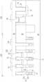
图19A所绘示的为图18中的接触结构的立体图,图19B所绘示的为接触结构的立体图的变化型,图20所绘示的是图19A的立体分解图。虽然图20中只显示了图19A的立体分解图,但是图19B的立体分解图和图19A类似,差别只在于第一部件面积的大小,其余的元件相对位置都相同,因此图19B的立体分解图请参酌图19A的立体分解图。FIG. 19A is a perspective view of the contact structure in FIG. 18 , FIG. 19B is a modified version of the contact structure, and FIG. 20 is an exploded perspective view of FIG. 19A . Although only the exploded perspective view of FIG. 19A is shown in FIG. 20 , the exploded perspective view of FIG. 19B is similar to that of FIG. 19A , the only difference being the size of the area of the first component, and the relative positions of the rest of the components are the same, so the perspective exploded view of FIG. 19B Please refer to the exploded perspective view of FIG. 19A.
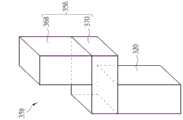
如图19A和图20所示,一个接触结构358包含一电容连接垫356和一电容接触插塞320。电容连接垫356包含一第一部件368和一第二部件370,第二部件370位于第一部件368和电容接触插塞320之间,第一部件368包含一第一底面372,第二部件370包含一第一顶面374和一第二底面376,其中第一底面372接触第一顶面374,第一底面372的面积小于第一顶面374的面积,电容接触插塞320包含第二顶面378,第二顶面378接触第二底面376,第二顶面378的面积小于第二底面376的面积。第一部件368和电容接触插塞320交错,第一底面372完全不重叠第二顶面378,其中第一顶面374和第二底面376相对并且具有相同形状和面积。As shown in FIGS. 19A and 20 , a
如图19B和图19A的不同之处在于,图19B的第二顶面378仅部分重叠第一底面372,而图19A中的第一底面372完全不重叠第二顶面378,此不同之处主要是由于图16中光掩模328的位置不同所造成。The difference between FIG. 19B and FIG. 19A is that the second
相较于传统的电容连接垫,本发明的电容连接垫的制作过程经过修整以将部分的导电材料移除,使得电容连接垫的第一部件的第一底面小于第二部件的第一顶面,如此可以让电容和其相邻的第一部件之间的距离增加,降低短路的机会。Compared with the traditional capacitor connection pad, the manufacturing process of the capacitor connection pad of the present invention is trimmed to remove part of the conductive material, so that the first bottom surface of the first part of the capacitor connection pad is smaller than the first top surface of the second part , so that the distance between the capacitor and its adjacent first component can be increased, reducing the chance of short circuit.
以上所述仅为本发明的优选实施例,凡依本发明权利要求所做的均等变化与修饰,都应属本发明的涵盖范围。The above descriptions are only preferred embodiments of the present invention, and all equivalent changes and modifications made according to the claims of the present invention shall fall within the scope of the present invention.
Claims (11)
Priority Applications (5)
| Application Number | Priority Date | Filing Date | Title |
|---|---|---|---|
| CN202010673242.2ACN111799261B (en) | 2017-02-24 | 2017-02-24 | Semiconductor structure with capacitive connection pads and method for making capacitive connection pads |
| CN201710102423.8ACN108511440B (en) | 2017-02-24 | 2017-02-24 | Semiconductor structure with capacitor connection pad and method of making capacitor connection pad |
| US15/889,182US11049863B2 (en) | 2017-02-24 | 2018-02-05 | Semiconductor structure with capacitor landing pad and method of making the same |
| US17/324,114US11563012B2 (en) | 2017-02-24 | 2021-05-19 | Semiconductor structure with capacitor landing pad and method of making the same |
| US18/076,419US11765881B2 (en) | 2017-02-24 | 2022-12-07 | Semiconductor structure with capacitor landing pad and method of making the same |
Applications Claiming Priority (1)
| Application Number | Priority Date | Filing Date | Title |
|---|---|---|---|
| CN201710102423.8ACN108511440B (en) | 2017-02-24 | 2017-02-24 | Semiconductor structure with capacitor connection pad and method of making capacitor connection pad |
Related Child Applications (1)
| Application Number | Title | Priority Date | Filing Date |
|---|---|---|---|
| CN202010673242.2ADivisionCN111799261B (en) | 2017-02-24 | 2017-02-24 | Semiconductor structure with capacitive connection pads and method for making capacitive connection pads |
Publications (2)
| Publication Number | Publication Date |
|---|---|
| CN108511440A CN108511440A (en) | 2018-09-07 |
| CN108511440Btrue CN108511440B (en) | 2020-12-01 |
Family
ID=63246957
Family Applications (2)
| Application Number | Title | Priority Date | Filing Date |
|---|---|---|---|
| CN202010673242.2AActiveCN111799261B (en) | 2017-02-24 | 2017-02-24 | Semiconductor structure with capacitive connection pads and method for making capacitive connection pads |
| CN201710102423.8AActiveCN108511440B (en) | 2017-02-24 | 2017-02-24 | Semiconductor structure with capacitor connection pad and method of making capacitor connection pad |
Family Applications Before (1)
| Application Number | Title | Priority Date | Filing Date |
|---|---|---|---|
| CN202010673242.2AActiveCN111799261B (en) | 2017-02-24 | 2017-02-24 | Semiconductor structure with capacitive connection pads and method for making capacitive connection pads |
Country Status (2)
| Country | Link |
|---|---|
| US (3) | US11049863B2 (en) |
| CN (2) | CN111799261B (en) |
Cited By (2)
| Publication number | Priority date | Publication date | Assignee | Title |
|---|---|---|---|---|
| US11935785B2 (en) | 2021-07-19 | 2024-03-19 | Changxin Memory Technologies, Inc. | Method of manufacturing a semiconductor structure, and a semiconductor structure |
| US12336161B2 (en) | 2021-09-17 | 2025-06-17 | Changxin Memory Technologies, Inc. | Semiconductor structure and manufacturing method thereof |
Families Citing this family (12)
| Publication number | Priority date | Publication date | Assignee | Title |
|---|---|---|---|---|
| CN110707085B (en)* | 2018-09-07 | 2022-05-03 | 联华电子股份有限公司 | Semiconductor device and method of forming the same |
| US11011522B2 (en)* | 2019-09-25 | 2021-05-18 | Nanya Technologies Corporation | Semiconductor device with nanowire capacitor plugs and method for fabricating the same |
| CN114496926B (en) | 2020-10-23 | 2024-12-10 | 长鑫存储技术有限公司 | Semiconductor structure manufacturing method and semiconductor structure |
| CN114420641B (en)* | 2020-10-28 | 2024-06-07 | 长鑫存储技术有限公司 | Method for forming semiconductor structure and semiconductor structure |
| US11869931B2 (en) | 2021-01-27 | 2024-01-09 | Changxin Memory Technologies, Inc. | Semiconductor structure and method of forming the same |
| CN113035872B (en)* | 2021-03-05 | 2023-04-07 | 长鑫存储技术有限公司 | Semiconductor structure and manufacturing method thereof |
| EP4287256A4 (en) | 2021-03-05 | 2024-08-28 | Changxin Memory Technologies, Inc. | SEMICONDUCTOR STRUCTURE AND ITS MANUFACTURING METHOD |
| KR20230006736A (en) | 2021-07-02 | 2023-01-11 | 삼성전자주식회사 | Semiconductor memory device and method of morming the same |
| TWI798920B (en)* | 2021-11-05 | 2023-04-11 | 力晶積成電子製造股份有限公司 | Manufacturing method of pad |
| TWI824387B (en)* | 2022-01-19 | 2023-12-01 | 華邦電子股份有限公司 | Method for forming semiconductor memory structure |
| US11830812B2 (en)* | 2022-04-08 | 2023-11-28 | Nanya Technology Corporation | Semiconductor device with T-shaped landing pad structure |
| CN114628504A (en)* | 2022-04-29 | 2022-06-14 | 长鑫存储技术有限公司 | Semiconductor structure and manufacturing method thereof |
Citations (1)
| Publication number | Priority date | Publication date | Assignee | Title |
|---|---|---|---|---|
| CN102479803A (en)* | 2010-11-30 | 2012-05-30 | 尔必达存储器株式会社 | Semiconductor device and method of forming the same |
Family Cites Families (11)
| Publication number | Priority date | Publication date | Assignee | Title |
|---|---|---|---|---|
| JP3577195B2 (en)* | 1997-05-15 | 2004-10-13 | 株式会社ルネサステクノロジ | Semiconductor device and manufacturing method thereof |
| JP4249765B2 (en)* | 2006-07-05 | 2009-04-08 | エルピーダメモリ株式会社 | Semiconductor device and manufacturing method thereof |
| US7864561B2 (en)* | 2006-07-28 | 2011-01-04 | Taiwan Semiconductor Manufacturing Co., Ltd. | Cell structure with buried capacitor for soft error rate improvement |
| KR101406225B1 (en)* | 2008-04-11 | 2014-06-13 | 삼성전자주식회사 | Method of fabricating a semiconductor device |
| KR101006531B1 (en)* | 2009-05-11 | 2011-01-07 | 주식회사 하이닉스반도체 | Semiconductor device and manufacturing method |
| US8884308B2 (en)* | 2011-11-29 | 2014-11-11 | Taiwan Semiconductor Manufacturing Company, Ltd. | High electron mobility transistor structure with improved breakdown voltage performance |
| KR20130089120A (en)* | 2012-02-01 | 2013-08-09 | 에스케이하이닉스 주식회사 | Methods for fabricating semiconductor device with fine pattenrs |
| KR101926027B1 (en)* | 2012-08-31 | 2018-12-06 | 에스케이하이닉스 주식회사 | Semiconductor device having asymmetry bit line contact and method for manufacturing the same |
| US9425200B2 (en)* | 2013-11-07 | 2016-08-23 | SK Hynix Inc. | Semiconductor device including air gaps and method for fabricating the same |
| KR102198857B1 (en)* | 2014-01-24 | 2021-01-05 | 삼성전자 주식회사 | Semiconductor device having landing pad |
| KR102171267B1 (en)* | 2014-01-28 | 2020-10-28 | 삼성전자 주식회사 | Semiconductor device having landing pad |
- 2017
- 2017-02-24CNCN202010673242.2Apatent/CN111799261B/enactiveActive
- 2017-02-24CNCN201710102423.8Apatent/CN108511440B/enactiveActive
- 2018
- 2018-02-05USUS15/889,182patent/US11049863B2/enactiveActive
- 2021
- 2021-05-19USUS17/324,114patent/US11563012B2/enactiveActive
- 2022
- 2022-12-07USUS18/076,419patent/US11765881B2/enactiveActive
Patent Citations (1)
| Publication number | Priority date | Publication date | Assignee | Title |
|---|---|---|---|---|
| CN102479803A (en)* | 2010-11-30 | 2012-05-30 | 尔必达存储器株式会社 | Semiconductor device and method of forming the same |
Cited By (2)
| Publication number | Priority date | Publication date | Assignee | Title |
|---|---|---|---|---|
| US11935785B2 (en) | 2021-07-19 | 2024-03-19 | Changxin Memory Technologies, Inc. | Method of manufacturing a semiconductor structure, and a semiconductor structure |
| US12336161B2 (en) | 2021-09-17 | 2025-06-17 | Changxin Memory Technologies, Inc. | Semiconductor structure and manufacturing method thereof |
Also Published As
| Publication number | Publication date |
|---|---|
| CN108511440A (en) | 2018-09-07 |
| CN111799261A (en) | 2020-10-20 |
| US11765881B2 (en) | 2023-09-19 |
| CN111799261B (en) | 2023-07-18 |
| US20210272962A1 (en) | 2021-09-02 |
| US11563012B2 (en) | 2023-01-24 |
| US11049863B2 (en) | 2021-06-29 |
| US20180247943A1 (en) | 2018-08-30 |
| US20230097175A1 (en) | 2023-03-30 |
Similar Documents
| Publication | Publication Date | Title |
|---|---|---|
| CN108511440B (en) | Semiconductor structure with capacitor connection pad and method of making capacitor connection pad | |
| CN110707085B (en) | Semiconductor device and method of forming the same | |
| CN110581103B (en) | Semiconductor element and manufacturing method thereof | |
| US8372724B2 (en) | Device and manufacturing method thereof | |
| US11653491B2 (en) | Contacts and method of manufacturing the same | |
| US10593677B2 (en) | Semiconductor structure with capacitor landing pad and method of make the same | |
| JP5073157B2 (en) | Semiconductor device | |
| US9299827B2 (en) | Semiconductor integrated circuit devices including gates having connection lines thereon | |
| CN108573971B (en) | Semiconductor memory structure | |
| CN108231769B (en) | Semiconductor element and manufacturing method thereof | |
| US8592978B2 (en) | Method of fabricating semiconductor device and the semiconductor device | |
| TWI781559B (en) | Semiconductor devices | |
| US7250335B2 (en) | Methods of fabricating integrated circuit devices including self-aligned contacts with increased alignment margin | |
| US11665888B2 (en) | Semiconductor device and method for fabricating the same | |
| US20090258488A1 (en) | Methods of fabricating semiconductor devices including storage node landing pads separated from bit line contact plugs | |
| US9349813B2 (en) | Method for fabricating semiconductor device | |
| US20240244822A1 (en) | Semiconductor structure and manufacturing method thereof | |
| KR20070013072A (en) | DRAM device having capacitors and manufacturing method thereof | |
| KR20060091599A (en) | Semiconductor device having landing pad and manufacturing method thereof | |
| KR20040043955A (en) | DRAM device and fabrication method thereof |
Legal Events
| Date | Code | Title | Description |
|---|---|---|---|
| PB01 | Publication | ||
| PB01 | Publication | ||
| SE01 | Entry into force of request for substantive examination | ||
| SE01 | Entry into force of request for substantive examination | ||
| CB02 | Change of applicant information | ||
| CB02 | Change of applicant information | Address after:Hsinchu City, Taiwan, China Applicant after:UNITED MICROELECTRONICS Corp. Applicant after:Fujian Jinhua Integrated Circuit Co.,Ltd. Address before:Hsinchu Science Industrial Park, Hsinchu City, Taiwan, China Applicant before:UNITED MICROELECTRONICS Corp. Applicant before:Fujian Jinhua Integrated Circuit Co.,Ltd. | |
| GR01 | Patent grant | ||
| GR01 | Patent grant |