CN108495957B - SiC single crystal substrate - Google Patents
SiC single crystal substrateDownload PDFInfo
- Publication number
- CN108495957B CN108495957BCN201780007967.4ACN201780007967ACN108495957BCN 108495957 BCN108495957 BCN 108495957BCN 201780007967 ACN201780007967 ACN 201780007967ACN 108495957 BCN108495957 BCN 108495957B
- Authority
- CN
- China
- Prior art keywords
- intensity distribution
- rays
- detector
- energy
- intensity
- Prior art date
- Legal status (The legal status is an assumption and is not a legal conclusion. Google has not performed a legal analysis and makes no representation as to the accuracy of the status listed.)
- Active
Links
- 239000013078crystalSubstances0.000titleclaimsdescription137
- 239000000758substrateSubstances0.000titleclaimsdescription33
- 238000009826distributionMethods0.000claimsabstractdescription152
- 238000005259measurementMethods0.000claimsabstractdescription53
- 229910010271silicon carbideInorganic materials0.000claimsdescription122
- HBMJWWWQQXIZIP-UHFFFAOYSA-Nsilicon carbideChemical compound[Si+]#[C-]HBMJWWWQQXIZIP-UHFFFAOYSA-N0.000claimsdescription121
- 238000000034methodMethods0.000claimsdescription22
- 238000004519manufacturing processMethods0.000claimsdescription10
- 238000005092sublimation methodMethods0.000claimsdescription2
- 230000005855radiationEffects0.000description24
- 239000000463materialSubstances0.000description22
- 239000012212insulatorSubstances0.000description6
- 239000012530fluidSubstances0.000description5
- 238000004088simulationMethods0.000description5
- IJGRMHOSHXDMSA-UHFFFAOYSA-NAtomic nitrogenChemical compoundN#NIJGRMHOSHXDMSA-UHFFFAOYSA-N0.000description4
- 239000007789gasSubstances0.000description3
- XKRFYHLGVUSROY-UHFFFAOYSA-NArgonChemical compound[Ar]XKRFYHLGVUSROY-UHFFFAOYSA-N0.000description2
- XUIMIQQOPSSXEZ-UHFFFAOYSA-NSiliconChemical group[Si]XUIMIQQOPSSXEZ-UHFFFAOYSA-N0.000description2
- 125000004432carbon atomChemical groupC*0.000description2
- 238000010438heat treatmentMethods0.000description2
- 229910052757nitrogenInorganic materials0.000description2
- 230000004308accommodationEffects0.000description1
- 239000000853adhesiveSubstances0.000description1
- 230000001070adhesive effectEffects0.000description1
- 229910052786argonInorganic materials0.000description1
- 230000009286beneficial effectEffects0.000description1
- 238000005520cutting processMethods0.000description1
- 230000003247decreasing effectEffects0.000description1
- 239000001307heliumSubstances0.000description1
- 229910052734heliumInorganic materials0.000description1
- SWQJXJOGLNCZEY-UHFFFAOYSA-Nhelium atomChemical compound[He]SWQJXJOGLNCZEY-UHFFFAOYSA-N0.000description1
- 239000012535impuritySubstances0.000description1
- 230000006698inductionEffects0.000description1
- 239000011261inert gasSubstances0.000description1
- 238000012986modificationMethods0.000description1
- 230000004048modificationEffects0.000description1
- 229910021420polycrystalline siliconInorganic materials0.000description1
- 239000002994raw materialSubstances0.000description1
- 229910052703rhodiumInorganic materials0.000description1
- 239000010948rhodiumSubstances0.000description1
- MHOVAHRLVXNVSD-UHFFFAOYSA-Nrhodium atomChemical compound[Rh]MHOVAHRLVXNVSD-UHFFFAOYSA-N0.000description1
- 238000000859sublimationMethods0.000description1
- 230000008022sublimationEffects0.000description1
Images


Classifications
- C—CHEMISTRY; METALLURGY
- C30—CRYSTAL GROWTH
- C30B—SINGLE-CRYSTAL GROWTH; UNIDIRECTIONAL SOLIDIFICATION OF EUTECTIC MATERIAL OR UNIDIRECTIONAL DEMIXING OF EUTECTOID MATERIAL; REFINING BY ZONE-MELTING OF MATERIAL; PRODUCTION OF A HOMOGENEOUS POLYCRYSTALLINE MATERIAL WITH DEFINED STRUCTURE; SINGLE CRYSTALS OR HOMOGENEOUS POLYCRYSTALLINE MATERIAL WITH DEFINED STRUCTURE; AFTER-TREATMENT OF SINGLE CRYSTALS OR A HOMOGENEOUS POLYCRYSTALLINE MATERIAL WITH DEFINED STRUCTURE; APPARATUS THEREFOR
- C30B29/00—Single crystals or homogeneous polycrystalline material with defined structure characterised by the material or by their shape
- C30B29/10—Inorganic compounds or compositions
- C30B29/36—Carbides
- G—PHYSICS
- G01—MEASURING; TESTING
- G01N—INVESTIGATING OR ANALYSING MATERIALS BY DETERMINING THEIR CHEMICAL OR PHYSICAL PROPERTIES
- G01N23/00—Investigating or analysing materials by the use of wave or particle radiation, e.g. X-rays or neutrons, not covered by groups G01N3/00 – G01N17/00, G01N21/00 or G01N22/00
- G01N23/20—Investigating or analysing materials by the use of wave or particle radiation, e.g. X-rays or neutrons, not covered by groups G01N3/00 – G01N17/00, G01N21/00 or G01N22/00 by using diffraction of the radiation by the materials, e.g. for investigating crystal structure; by using scattering of the radiation by the materials, e.g. for investigating non-crystalline materials; by using reflection of the radiation by the materials
- G01N23/207—Diffractometry using detectors, e.g. using a probe in a central position and one or more displaceable detectors in circumferential positions
- H—ELECTRICITY
- H01—ELECTRIC ELEMENTS
- H01L—SEMICONDUCTOR DEVICES NOT COVERED BY CLASS H10
- H01L21/00—Processes or apparatus adapted for the manufacture or treatment of semiconductor or solid state devices or of parts thereof
- H01L21/02—Manufacture or treatment of semiconductor devices or of parts thereof
- H01L21/02002—Preparing wafers
- C—CHEMISTRY; METALLURGY
- C01—INORGANIC CHEMISTRY
- C01B—NON-METALLIC ELEMENTS; COMPOUNDS THEREOF; METALLOIDS OR COMPOUNDS THEREOF NOT COVERED BY SUBCLASS C01C
- C01B32/00—Carbon; Compounds thereof
- C01B32/90—Carbides
- C01B32/914—Carbides of single elements
- C01B32/956—Silicon carbide
- C—CHEMISTRY; METALLURGY
- C01—INORGANIC CHEMISTRY
- C01P—INDEXING SCHEME RELATING TO STRUCTURAL AND PHYSICAL ASPECTS OF SOLID INORGANIC COMPOUNDS
- C01P2002/00—Crystal-structural characteristics
- C01P2002/70—Crystal-structural characteristics defined by measured X-ray, neutron or electron diffraction data
- C01P2002/72—Crystal-structural characteristics defined by measured X-ray, neutron or electron diffraction data by d-values or two theta-values, e.g. as X-ray diagram
- C—CHEMISTRY; METALLURGY
- C30—CRYSTAL GROWTH
- C30B—SINGLE-CRYSTAL GROWTH; UNIDIRECTIONAL SOLIDIFICATION OF EUTECTIC MATERIAL OR UNIDIRECTIONAL DEMIXING OF EUTECTOID MATERIAL; REFINING BY ZONE-MELTING OF MATERIAL; PRODUCTION OF A HOMOGENEOUS POLYCRYSTALLINE MATERIAL WITH DEFINED STRUCTURE; SINGLE CRYSTALS OR HOMOGENEOUS POLYCRYSTALLINE MATERIAL WITH DEFINED STRUCTURE; AFTER-TREATMENT OF SINGLE CRYSTALS OR A HOMOGENEOUS POLYCRYSTALLINE MATERIAL WITH DEFINED STRUCTURE; APPARATUS THEREFOR
- C30B29/00—Single crystals or homogeneous polycrystalline material with defined structure characterised by the material or by their shape
- C30B29/60—Single crystals or homogeneous polycrystalline material with defined structure characterised by the material or by their shape characterised by shape
- C30B29/64—Flat crystals, e.g. plates, strips or discs
Landscapes
- Chemical & Material Sciences (AREA)
- Engineering & Computer Science (AREA)
- Crystallography & Structural Chemistry (AREA)
- Inorganic Chemistry (AREA)
- Materials Engineering (AREA)
- Metallurgy (AREA)
- Organic Chemistry (AREA)
- Physics & Mathematics (AREA)
- General Physics & Mathematics (AREA)
- General Health & Medical Sciences (AREA)
- Analytical Chemistry (AREA)
- Biochemistry (AREA)
- Life Sciences & Earth Sciences (AREA)
- Health & Medical Sciences (AREA)
- Immunology (AREA)
- Pathology (AREA)
- Condensed Matter Physics & Semiconductors (AREA)
- Manufacturing & Machinery (AREA)
- Computer Hardware Design (AREA)
- Microelectronics & Electronic Packaging (AREA)
- Power Engineering (AREA)
- Analysing Materials By The Use Of Radiation (AREA)
- Crystals, And After-Treatments Of Crystals (AREA)
- Length-Measuring Devices Using Wave Or Particle Radiation (AREA)
Abstract
Description
Translated fromChinese技术领域technical field
本发明涉及一种碳化硅单晶衬底。本申请主张基于2016年2月9日提交的日本专利申请2016-022388号的优先权,其全部内容以引用的形式并入本文中。The invention relates to a silicon carbide single crystal substrate. This application claims priority based on Japanese Patent Application No. 2016-022388 filed on February 9, 2016, the entire contents of which are incorporated herein by reference.
背景技术Background technique
例如,日本专利特许公开2009-120419号公报(专利文献1)描述了一种使用升华法制造碳化硅单晶的方法。For example, Japanese Patent Laid-Open Publication No. 2009-120419 (Patent Document 1) describes a method of producing a silicon carbide single crystal using a sublimation method.
现有技术文献prior art literature
专利文献patent documents
专利文献1:日本专利特许公开2009-120419号公报Patent Document 1: Japanese Patent Laid-Open Publication No. 2009-120419
发明内容Contents of the invention
根据本发明的碳化硅单晶衬底包含相对于(0001)面在<11-20>方向上倾斜的主面。在沿与主面垂直的方向观察时检测器配置于[11-20]方向上、在相对于[-1-120]方向在±15°以内的方向上用X射线照射包括主面的中心的第一测量区域、且使用所述检测器测量来自所述第一测量区域的衍射X射线的情况下,在6.9keV~11.7keV范围内所述衍射X射线的第一强度分布的最大强度对所述第一强度分布的背景强度之比大于或等于1500。在沿与主面垂直的方向观察时检测器配置于平行于[-1100]方向的方向、在相对于[1-100]方向在±6°以内的方向上用X射线照射第一测量区域、且使用所述检测器测量来自所述第一测量区域的衍射X射线的情况下,在8.0keV~9.5keV范围内所述衍射X射线的第二强度分布的最大强度对所述第二强度分布的背景强度之比大于或等于1500。在沿与主面垂直的方向观察时检测器配置于[11-20]方向上并且要用X射线照射的位置在相对于[-1-120]方向在±15°以内的范围内变化的情况下,在所述第一强度分布指示在6.9keV~11.7keV范围内的最大值时的能量的最大值与最小值之差的绝对值小于或等于0.06keV。The silicon carbide single crystal substrate according to the present invention includes a main surface inclined in the <11-20> direction with respect to the (0001) plane. The detector is arranged in the [11-20] direction when viewed in a direction perpendicular to the main surface, and the center of the main surface is irradiated with X-rays in a direction within ±15° relative to the [-1-120] direction In the case of the first measurement area and using the detector to measure the diffracted X-rays from the first measurement area, the maximum intensity of the first intensity distribution of the diffracted X-rays in the range of 6.9keV to 11.7keV is The background intensity ratio of the first intensity distribution is greater than or equal to 1500. The detector is arranged in a direction parallel to the [-1100] direction when viewed in a direction perpendicular to the main surface, and the first measurement region is irradiated with X-rays in a direction within ±6° relative to the [1-100] direction, And when the detector is used to measure the diffracted X-rays from the first measurement area, the maximum intensity of the second intensity distribution of the diffracted X-rays in the range of 8.0keV to 9.5keV is relatively large to the second intensity distribution The background intensity ratio is greater than or equal to 1500. The case where the detector is arranged in the [11-20] direction and the position to be irradiated with X-rays changes within ±15° with respect to the [-1-120] direction when viewed in a direction perpendicular to the main surface Here, an absolute value of a difference between a maximum value and a minimum value of energy when the first intensity distribution indicates a maximum value within a range of 6.9 keV to 11.7 keV is less than or equal to 0.06 keV.
附图说明Description of drawings
图1是显示根据本实施方案的碳化硅单晶衬底的构造的示意性平面图。FIG. 1 is a schematic plan view showing the configuration of a silicon carbide single crystal substrate according to the present embodiment.
图2是显示根据本实施方案的碳化硅单晶衬底的构造的示意性横截面图。Fig. 2 is a schematic cross-sectional view showing the configuration of a silicon carbide single crystal substrate according to the present embodiment.
图3是显示用于测量第一强度分布的方法的示意性正视图。Fig. 3 is a schematic front view showing a method for measuring a first intensity distribution.
图4是显示用于测量第一强度分布的方法的示意性平面图。Fig. 4 is a schematic plan view showing a method for measuring a first intensity distribution.
图5显示了示例性的第一强度分布。Figure 5 shows an exemplary first intensity distribution.
图6是显示用于测量第一强度分布的方法的示意性平面图。Fig. 6 is a schematic plan view showing a method for measuring a first intensity distribution.
图7是显示用于测量第一强度分布的方法的示意性平面图。Fig. 7 is a schematic plan view showing a method for measuring a first intensity distribution.
图8显示了示例性的第一强度分布。Figure 8 shows an exemplary first intensity distribution.
图9显示了检测器的角度与指示第一强度分布的最大值时的能量之间的关系。Figure 9 shows the relationship between the angle of the detector and the energy at which the maximum value of the first intensity distribution is indicated.
图10是显示用于测量第二强度分布的方法的示意性正视图。Fig. 10 is a schematic front view showing a method for measuring the second intensity distribution.
图11是显示用于测量第二强度分布的方法的示意性平面图。Fig. 11 is a schematic plan view showing a method for measuring the second intensity distribution.
图12显示了示例性的第二强度分布。Figure 12 shows an exemplary second intensity distribution.
图13是显示用于测量第二强度分布的方法的示意性平面图。Fig. 13 is a schematic plan view showing a method for measuring the second intensity distribution.
图14是显示用于测量第二强度分布的方法的示意性平面图。Fig. 14 is a schematic plan view showing a method for measuring the second intensity distribution.
图15显示了示例性的第二强度分布。Figure 15 shows an exemplary second intensity distribution.
图16显示了检测器的角度与指示第二强度分布的最大值时的能量之间的关系。Figure 16 shows the relationship between the angle of the detector and the energy at which the maximum value of the second intensity distribution is indicated.
图17是显示用于测量第三强度分布的方法的示意性平面图。Fig. 17 is a schematic plan view showing a method for measuring the third intensity distribution.
图18显示了示例性的第三强度分布。Figure 18 shows an exemplary third intensity distribution.
图19是显示用于测量第四强度分布的方法的示意性平面图。Fig. 19 is a schematic plan view showing a method for measuring the fourth intensity distribution.
图20显示了示例性的第四强度分布。Figure 20 shows an exemplary fourth intensity distribution.
图21是显示用于碳化硅单晶锭(ingot)的制造设备的构造的示意性横截面图。Fig. 21 is a schematic cross-sectional view showing the configuration of a manufacturing apparatus for a silicon carbide single crystal ingot.
图22是显示用于制造碳化硅单晶衬底的方法的示意性横截面图。Fig. 22 is a schematic cross-sectional view showing a method for manufacturing a silicon carbide single crystal substrate.
图23显示了在生长碳化硅单晶的步骤中加热器功率与碳化硅单晶长度之间的关系。Fig. 23 shows the relationship between the heater power and the length of the silicon carbide single crystal in the step of growing the silicon carbide single crystal.
具体实施方式Detailed ways
[本发明要解决的问题][Problems to be Solved by the Invention]
本发明的目的是提供一种应变减小的碳化硅单晶衬底。An object of the present invention is to provide a silicon carbide single crystal substrate with reduced strain.
[本发明的有益效果][Beneficial effects of the present invention]
根据本发明,能够提供应变减小的碳化硅单晶衬底。According to the present invention, a strain-reduced silicon carbide single crystal substrate can be provided.
[本发明实施方案的概要][Summary of Embodiments of the Present Invention]
首先,下文对本发明实施方案的概要进行说明。关于本说明书中的结晶学指示,单个取向由[]表示,组的取向由<>表示,并且单个面由()表示,且组的面由{}表示。负指数应该通过将“-”(横号(bar))置于数字之上来进行晶体学指示,但是在本说明书中通过将负号放在数字之前来指示。First, an outline of an embodiment of the present invention will be described below. Regarding crystallographic indications in this specification, a single orientation is represented by [], a group of orientations is represented by <>, and a single plane is represented by (), and a group of planes is represented by {}. Negative indices should be indicated crystallographically by placing a "-" (bar) above the number, but are indicated in this specification by placing a minus sign before the number.
(1)根据本发明的碳化硅单晶衬底包含相对于(0001)面在<11-20>方向上倾斜的主面11。在沿与主面11垂直的方向观察时检测器6配置于[11-20]方向上、在相对于[-1-120]方向在±15°以内的方向上用X射线照射包括主面11的中心的第一测量区域31、且使用所述检测器6测量源自所述第一测量区域31的衍射X射线的情况下,在6.9keV~11.7keV范围内所述衍射X射线的第一强度分布1的最大强度对第一强度分布1的背景强度之比大于或等于1500。在沿与主面11垂直的方向观察时检测器6配置于平行于[-1100]方向的方向上、在相对于[1-100]方向在±6°以内的方向上用X射线照射第一测量区域31、且使用检测器6测量源自第一测量区域31的衍射X射线的情况下,在8.0keV~9.5keV范围内所述衍射X射线的第二强度分布2的最大强度对第二强度分布2的背景强度之比大于或等于1500。在沿与主面11垂直的方向观察时检测器6配置于[11-20]方向上并且要用X射线照射的位置在相对于[-1-120]方向在±15°以内的范围内变化的情况下,在所述第一强度分布1指示在6.9keV~11.7keV范围内的最大值时能量的最大值EH1与最小值EL1之差的绝对值小于或等于0.06keV。(1) The silicon carbide single crystal substrate according to the present invention includes
通常,通过以使得碳化硅单晶衬底具有对应于期望面(例如相对于(0001)面倾斜4°的面)的主面的方式切割碳化硅单晶锭,得到碳化硅单晶衬底。在对实际碳化硅单晶衬底的晶格排列的详细分析中,将晶格对准以在碳化硅单晶衬底的主面中形成期望的面;然而,在高指数晶面中,晶格可能未对准以形成六方晶系碳化硅的理论晶格面。具体地,例如在理想的六方晶系碳化硅的情况下,硅原子或碳原子排列在由下述晶面(1)表示的特定的高指数晶面中。然而,在实际的六方晶系碳化硅的情况下,硅原子或碳原子可能不排列在上述特定的高指数晶面中,且可以排列在相对于上述特定的高指数晶面倾斜的平面中。这大概是由于如下原因:碳化硅单晶衬底内部的晶格排列是三维应变的(strained),因此偏离了六方晶系碳化硅的理论晶格排列。应注意,高指数晶面例如是指(1-10X)面(X=3、5、7、10等)。Usually, a silicon carbide single crystal ingot is obtained by cutting a silicon carbide single crystal ingot in such a manner that the silicon carbide single crystal substrate has a main surface corresponding to a desired plane (for example, a plane inclined at 4° with respect to the (0001) plane). In a detailed analysis of the lattice arrangement of an actual SiC single-crystal substrate, the lattices are aligned to form the desired facets in the main face of the SiC single-crystal substrate; however, in high-index crystallographic planes, the crystallographic The lattice may be misaligned to form the theoretical lattice planes of hexagonal silicon carbide. Specifically, for example, in the case of ideal hexagonal silicon carbide, silicon atoms or carbon atoms are arranged in a specific high-index crystal plane represented by crystal plane (1) described below. However, in the case of actual hexagonal silicon carbide, silicon atoms or carbon atoms may not be arranged in the above-mentioned specific high-index crystal plane, and may be arranged in a plane inclined with respect to the above-mentioned specific high-index crystal plane. This is presumably due to the following reason: the lattice arrangement inside the silicon carbide single crystal substrate is three-dimensionally strained (strained), thus deviating from the theoretical lattice arrangement of hexagonal silicon carbide. It should be noted that a high-index crystal plane refers to, for example, a (1-10X) plane (X=3, 5, 7, 10, etc.).
[式1][Formula 1]
(1-1010)……晶面(1)(1-1010)……Crystal surface(1)
为了获得具有小三维应变的高质量碳化硅单晶衬底,期望的是,在生长碳化硅单晶锭的过程中在晶体表面的热环境的变化小的条件下进行碳化硅单晶锭的生长,同时保持其生长表面尽可能平坦。为了实现这种晶体生长环境,例如考虑:使用具有5区结构的加热器的碳化硅单晶制造设备;并单独控制加热器各自的加热器功率以降低碳化硅单晶锭的生长表面的温度分布并减少生长表面的温度变化。具体地,例如在其中碳化硅单晶锭的长度为0~25mm的范围内,每1mm进行热流体模拟,由此计算在锭的生长表面内和在源材料中的温度分布并计算坩埚周围的温度分布。然后,确定施加到加热器的各个加热器功率,以降低碳化硅单晶锭的生长表面和源材料中的温度分布并降低生长表面和源材料表面的温度变化。热流体模拟是例如使用构件如坩埚和隔热体、籽晶和碳化硅源材料的导热率和辐射率来计算炉内的温度分布。通过如下所述基于热流体模拟的结果来控制加热器各自的加热器功率,能够得到具有小应变的碳化硅单晶锭。结果,能够得到应变减小的碳化硅单晶衬底。In order to obtain a high-quality silicon carbide single crystal substrate with small three-dimensional strain, it is desirable that the growth of the silicon carbide single crystal ingot is carried out under the condition that the change in the thermal environment of the crystal surface is small during the growth of the silicon carbide single crystal ingot , while keeping its growth surface as flat as possible. In order to realize such a crystal growth environment, it is considered, for example: a silicon carbide single crystal manufacturing facility using heaters having a 5-zone structure; and individually controlling the respective heater powers of the heaters to reduce the temperature distribution of the growth surface of the silicon carbide single crystal ingot And reduce the temperature variation of the growth surface. Specifically, for example, in the range in which the length of the silicon carbide single crystal ingot is 0 to 25 mm, thermal fluid simulation is performed every 1 mm, thereby calculating the temperature distribution in the growth surface of the ingot and in the source material and calculating the temperature distribution around the crucible. Temperature Distribution. Then, the respective heater powers applied to the heaters are determined to reduce the temperature distribution in the growth surface and the source material of the silicon carbide single crystal ingot and to reduce the temperature variation of the growth surface and the source material surface. The thermal fluid simulation is to calculate the temperature distribution inside the furnace using, for example, the thermal conductivity and emissivity of components such as crucibles and insulators, seeds and silicon carbide source materials. By controlling the respective heater powers of the heaters based on the results of the thermal fluid simulation as described below, a silicon carbide single crystal ingot with a small strain can be obtained. As a result, a silicon carbide single crystal substrate with reduced strain can be obtained.
(2)在根据(1)所述的碳化硅单晶衬底10中,在沿与主面11垂直的方向观察时检测器6配置于与[-1100]方向平行的方向上并且要用X射线照射的位置在相对于[1-100]方向在±6°以内的范围内变化的情况下,在第二强度分布2指示在8.0keV~9.5keV的范围内的最大值时的能量的最大值EH2与最小值EL2之差的绝对值可以小于或等于0.08keV。(2) In the silicon carbide
(3)在根据(1)或(2)所述的碳化硅单晶衬底10中,主面11可以具有大于或等于100mm的最大直径。在沿与主面11垂直的方向观察时检测器6配置于[11-20]方向上、在相对于[-1-120]方向在±15°以内的方向上用X射线照射包括距主面11的外边缘10mm的位置的第二测量区域32、以及使用检测器6测量源自第二测量区域32的衍射X射线的情况下,在6.9keV~11.7keV范围内衍射X射线的第三强度分布3的最大强度对第三强度分布3的背景强度之比可以大于或等于1500。在沿与主面11垂直的方向观察时检测器6配置于[-1100]方向上、在相对于[1-100]方向在±6°以内的方向上用X射线照射第二测量区域32、且使用检测器6测量源自第二测量区域32的衍射X射线的情况下,在8.0keV~9.5keV范围内所述衍射X射线的第四强度分布4的最大强度对第四强度分布4的背景强度之比大于或等于1500。在沿与主面11垂直的方向观察时检测器6配置于[11-20]方向上并且要用X射线照射的位置在相对于[-1-120]方向在±15°以内的范围内变化的情况下,在第三强度分布3指示在6.9keV~11.7keV范围内的最大值时的能量的最大值与最小值之差的绝对值可以小于或等于0.06keV。(3) In silicon carbide
在制造具有最大直径大于或等于100mm的主面11的碳化硅单晶衬底10的情况下,与主面11的最大直径小于100mm的情况相比,更难以减少碳化硅单晶锭的生长表面的温度分布和减少生长表面的温度变化。根据下述方法,在具有最大直径大于或等于100mm的主面11的这种碳化硅单晶衬底中,应变也能够减小。In the case of manufacturing silicon carbide
(4)在根据(3)所述的碳化硅单晶衬底10中,在沿与主面11垂直的方向观察时检测器6配置于与[-1100]方向平行的方向上且要用X射线照射的位置相对于[1-100]方向在±6°以内的范围内变化的情况下,在第四强度分布4指示在8.0keV~9.5keV的范围内的最大值时的能量的最大值与最小值之差的绝对值可以小于或等于0.08keV。(4) In the silicon carbide
[本发明实施方案的细节][Details of Embodiments of the Invention]
下面将参考附图对本发明实施方案的细节进行描述。首先,将描述根据实施方案的碳化硅单晶衬底10的构造。应注意,在下述附图中,相同或相应的部分被赋予相同的附图标记,并且不再重复描述。Details of embodiments of the present invention will be described below with reference to the accompanying drawings. First, the configuration of silicon carbide
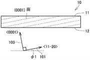
如图1和图2所示,根据本实施方案的碳化硅单晶衬底10主要包括:第一主面11;与第一主面11相反的第二主面12;和外边缘15。碳化硅单晶衬底10的外边缘15例如具有第一平坦部13和弯曲部14。例如,第一平坦部13沿着第一方向101延伸。外边缘15可以具有第二平坦部(未示出)。例如,第二平坦部沿与第一方向101垂直的第二方向102延伸。第一方向101例如是<11-20>方向。第二方向102例如是<1-100>方向。As shown in FIGS. 1 and 2 , silicon carbide
第一主面11对应于相对于(0001)面在偏离方向上倾斜的面。例如,第一主面11对应于相对于(0001)面倾斜大于或等于0.5°并且小于或等于8°的面。例如,偏离方向是<11-20>方向。例如,偏离方向可以是相对于(0001)面中的<11-20>方向倾斜±5°的角度的方向。偏离角φ1(参见图2)可以大于或等于1°或者可以大于或等于2°。偏离角φ1可以小于或等于7°或可能小于或等于6°。The first
碳化硅单晶衬底10由碳化硅单晶构成。例如,碳化硅单晶具有4H-SiC的多型。在电子迁移率、介电强度等方面,4H-SiC优于其他多型。碳化硅单晶衬底10例如包括诸如氮的n型杂质。碳化硅单晶衬底10的导电类型例如是n型。Silicon carbide
如图1所示,第一主面11具有大于或等于100mm的最大直径16(直径)。最大直径16可以大于或等于150mm,可以大于或等于200mm,或者可以大于或等于250mm。最大直径16的上限没有特别限制。例如,最大直径16的上限可以是300mm。As shown in FIG. 1 , the first
接着,下面对用于评价碳化硅单晶衬底10的三维应变的方法进行描述。Next, a method for evaluating the three-dimensional strain of silicon carbide
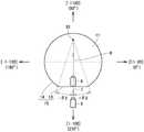
例如,通过使用由布鲁克公司(Bruker)提供的能量弥散型X射线衍射仪(型号:D2CRYSO),能够定量评价碳化硅单晶衬底10的三维应变。如图3所示,X射线发射器5和检测器6以面对第一主面11的方式配置。X射线发射器5以向第一主面11发射X射线的方式构造。X射线发射器5包括例如X射线管(铑)。例如,X射线发射器5以发射白色X射线的方式构造。检测器6以检测源自第一主面11的衍射X射线的方式构造。检测器6例如是能量弥散型检测器。For example, by using an energy dispersive X-ray diffractometer (model: D2CRYSO) provided by Bruker, the three-dimensional strain of silicon carbide
首先,下面将对用于测量平行于(0001)面的(0008)面的方法进行描述。First, a method for measuring the (0008) plane parallel to the (0001) plane will be described below.
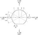
如图4所示,当从包括第一主面11的中心O的第一测量区域31观察时,X射线发射器5配置于[-1-120]方向上。假定当沿与第一主面11垂直的方向观察时,[11-20]方向、[-1100]方向、[-1-120]方向和[1-100]方向分别对应于0°、90°、180°和270°。当沿与第一主面11垂直的方向观察时,X射线发射器5配置于180°的位置处。入射的X射线7从X射线发射器5发射到第一测量区域31。当从包括第一主面11的中心O的第一测量区域31观察时,检测器6配置于[11-20]方向上。换言之,当沿与第一主面11垂直的方向观察时,检测器6配置于0°的位置处。通过检测器6测量由第一测量区域31衍射的衍射X射线8。As shown in FIG. 4 , when viewed from the
在第一主面11对应于相对于(0001)面在<11-20>方向上偏离4°角度的面的情况下,例如X射线发射器5相对于第一主面11的仰角φ3(换言之,入射的X射线7与第一主面11之间的角度φ3:参见图3)是29.889°。例如,检测器6相对于第一主面11的仰角φ2(换言之,衍射X射线8与第一主面11之间的角度φ2:参见图3)为67.765°。In the case where the first
在第一主面11对应于相对于(0001)面在<11-20>方向上偏离8°角度的面的情况下,例如X射线发射器5相对于第一主面11的仰角φ3(换言之,入射的X射线7与第一主面11之间的角度φ3:参见图3)是29.91°。例如,检测器6相对于第一主面11的仰角φ2(换言之,衍射X射线8与第一主面11之间的角度φ2:参见图3)为75.756°。In the case where the first
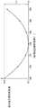
图5显示了利用如图4中所示配置的X射线发射器5和检测器6测量的衍射X射线的示例性强度分布(第一强度分布)。横轴代表衍射X射线的能量。纵轴代表衍射X射线的强度。如图5所示,第一强度分布1在第一能量E1与第二能量E2之间的能量处具有最大值。例如,第一能量E1是6.9keV。例如,第二能量E2是11.7keV。第一能量E1可以是7.7keV。第二能量E2可以是10.4keV。第一能量E1与第二能量E2之间的区域中的第一强度分布1的最大值由(0008)面产生。当第一主面11的偏离角改变时,指示强度分布的最大值时的能量发生改变。例如,在第一主面11对应于相对于(0001)面在<11-20>方向上偏离4°角度的面的情况下,对应于(0008)面的能量为8.84keV,而在第一主面11对应于相对于(0001)面在<11-20>方向上偏离8°角度的面的情况下,对应于(0008)面的能量为8.03keV。FIG. 5 shows an exemplary intensity distribution (first intensity distribution) of diffracted X-rays measured with the
基于第一强度分布1,测量在第一能量E1与第二能量E2之间的区域中强度分布的最大值的强度IP1及其背景强度IN1。背景强度IN1是例如在第二能量E2处强度分布的强度。类似地,在第一能量E1与第二能量E2之间,测量第一强度分布1指示最大值时的能量E(180°)。应注意,如图5所示,在第一能量E1与第二能量E2之间的区域中第一强度分布1的最大值的强度(约1.6)可以与整个测量范围内第一强度分布1的最大值的强度(约2.1)不同。Based on the
接着,X射线发射器5的位置在与第一主面11平行的面内变化。如图6所示,当沿与第一主面11垂直的方向观察时,X射线发射器5配置于(180-θ1)°的位置。例如,角度θ1是15°。即,当沿与第一主面11垂直的方向观察时,X射线发射器5配置于165°的位置。X射线发射器5相对于第一主面11的仰角φ3(参见图3)与其中X射线发射器5配置于180°位置的情况的相同。检测器6以与其中X射线发射器5配置于180°的位置的情况相同的方式配置。利用上述配置,利用源自X射线发射器5的入射X射线7对第一测量区域31进行照射,并通过检测器6测量由第一测量区域31衍射的衍射X射线8。Next, the position of the
因此,得到在其中X射线发射器5配置于165°位置的情况下的衍射X射线的第一强度分布。基于第一强度分布1,测量在第一能量E1与第二能量E2之间的区域中第一强度分布的最大值的强度IP1及其背景强度IN1。类似地,测量第一强度分布1指示最大值时的能量E(165°)。Thus, a first intensity distribution of diffracted X-rays is obtained in the case where the
接着,X射线发射器5的位置在与第一主面11平行的面内变化。如图7所示,当沿与第一主面11垂直的方向观察时,X射线发射器5位于(180+θ1)°的位置。例如,角度θ1是15°。即,当沿与第一主面11垂直的方向观察时,X射线发射器5配置于195°的位置。X射线发射器5相对于第一主面11的仰角φ3(参见图3)与其中X射线发射器5配置于180°位置的情况的相同。检测器6以与其中X射线发射器5配置于180°的位置的情况相同的方式配置。利用上述配置,利用源自X射线发射器5的入射X射线7对第一测量区域31进行照射,并通过检测器6测量由第一测量区域31衍射的衍射X射线8。Next, the position of the
因此,得到在其中X射线发射器5配置于195°位置的情况下的衍射X射线的第一强度分布。基于第一强度分布1,测量在第一能量E1与第二能量E2之间的区域中第一强度分布的最大值的强度IP1及其背景强度IN1。类似地,测量第一强度分布1指示最大值时的能量E(195°)。Thus, a first intensity distribution of diffracted X-rays is obtained in the case where the
如图8所示,在X射线发射器5配置于195°的位置的情况下第一强度分布1指示最大值时的能量E(195°)可以与在X射线发射器5配置于180°位置的情况下第一强度分布1指示最大值时的能量E(180°)不同。例如,当沿195°的方向观察时碳化硅的晶格的排列与当沿180°的方向观察时碳化硅的晶格的排列不同时,第一强度分布1指示最大值时的能量E(195°)与第一强度分布1指示最大值时的能量E(180°)不同。换言之,随着碳化硅单晶的三维应变越小,第一强度分布1指示最大值时的能量E(195°)与第一强度分布1指示最大值时的能量E(180°)之差越小。As shown in FIG. 8, the energy E(195°) when the
如上所述,通过在180°±15°以内的范围内以5°的间隔改变X射线发射器5的位置,测量七个第一强度分布。基于所述七个第一强度分布中的每一个,测量第一能量E1与第二能量E2之间的区域中第一强度分布的最大值的强度IP1及其背景强度IN1。在所有第一强度分布中的每一个中,第一强度分布1在6.9keV~11.7keV范围内的最大强度对第一强度分布1的背景强度之比(即IP1/IN1)大于或等于至1500,优选大于或等于2000,更优选大于或等于2500。As described above, seven first intensity distributions were measured by changing the position of the
换言之,在沿与主面11垂直的方向观察时检测器6配置于[11-20]方向上、在相对于[-1-120]方向在±15°以内的方向上用X射线照射包括主面11的中心O的第一测量区域31、以及使用检测器6测量源自第一测量区域31的衍射X射线的情况下,衍射X射线在6.9keV~11.7keV范围内的第一强度分布1的最大强度对第一强度分布1的背景强度之比大于或等于1500。In other words, the
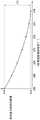
图9显示了在其中X射线发射器5的位置在第一主面11内改变的情况下指示第一强度分布的最大值时的能量。图9的纵轴代表在第一能量与第二能量之间指示第一强度分布的最大值时的能量。图9的横轴代表X射线发射器5的位置。当在180°±15°以内的范围内以5°的间隔改变X射线发射器5的位置时,对指示在6.9keV~11.7keV范围内衍射X射线的第一强度分布的最大值时的能量进行了测量。FIG. 9 shows the energy at which the maximum value of the first intensity distribution is indicated in the case where the position of the
如图9所示,当X射线发射器5的位置改变时,指示最大强度时的能量改变。当X射线发射器5相对于[-1-120]方向(即180°)在±15°以内的范围内以5°的间隔改变时,确定了在指示第一强度分布的最大值时的能量的最大值EH1和最小值EL1。当X射线发射器5相对于[-1-120]方向在±15°以内的范围内变化时,在第一强度分布1指示在6.9keV~11.7keV范围内的最大值时的能量的最大值EH1与最小值EL1之差的绝对值例如小于或等于0.06keV,优选小于或等于0.05keV,更优选小于或等于0.04keV。随着碳化硅单晶的三维应变越小,第一强度分布1指示最大值时的能量的最大值EH1与最小值EL1之差111的绝对值越小。As shown in FIG. 9, when the position of the
接着,下面将对用于测量由上述晶面(1)指示的特定高指数晶面的方法进行描述。换言之,上述特定高指数晶面是相对于(1-100)面在(0001)面方向上倾斜66°角度的面。Next, a method for measuring a specific high-index crystal plane indicated by the above crystal plane (1) will be described below. In other words, the above-mentioned specific high-index crystal plane is a plane inclined at an angle of 66° in the direction of the (0001) plane with respect to the (1-100) plane.
如图10所示,X射线发射器5和检测器6以面对第一主面11的方式配置。如图11所示,当从第一主面11的中心O观察时,X射线发射器5配置于[1-100]方向上。换言之,当沿与第一主面11垂直的方向观察时,X射线发射器5配置于270°的位置处。利用源自X射线发射器5的入射X射线7照射第一测量区域31。当从第一主面11的中心O观察时,检测器6配置于与[-1100]方向平行的方向上。换言之,当沿与第一主面11垂直的方向观察时,检测器6配置于90°或270°的位置处。由检测器6测量由第一测量区域31衍射的衍射X射线8。As shown in FIG. 10 ,
在第一主面11对应于相对于(0001)面在<11-20>方向上偏离4°角度的面的情况下,X射线发射器5相对于第一主面11的仰角φ3(换言之,入射的X射线7与第一主面11之间的角度φ3:参见图10)例如为29.907°。例如,检测器6相对于第一主面11的仰角φ2(换言之,衍射X射线8与第一主面11之间的角度φ2:参见图10)例如为101.810°。仰角φ2是在从[-1100]方向侧观察时的角度。在其中仰角φ2超过90°的情况下,当从中心O观察时,检测器6配置于与[-1100]方向相反的一侧。即,检测器6配置于270°的位置。In the case where the first
在第一主面11对应于相对于(0001)面在<11-20>方向上偏离8°角度的面的情况下,X射线发射器5相对于第一主面11的仰角φ3(换言之,入射的X射线7与第一主面11之间的角度φ3:参见图10)例如是29.91°。例如,检测器6相对于第一主面11的仰角φ2(换言之,衍射X射线8与第一主面11之间的角度φ2:参见图10)例如为103.939°。由于仰角φ2大于90°,所以检测器6配置于270°的位置。In the case where the first
图12显示了利用如图11中所示配置的X射线发射器5和检测器6测量的衍射X射线的示例性强度分布(第二强度分布)。横轴代表衍射X射线的能量。纵轴代表衍射X射线的强度。如图12所示,第二强度分布2在第三能量E3与第四能量E4之间的能量处具有最大值。例如,第三能量E3是8.0keV。例如,第四能量E4是9.5keV。第四能量E4可以是9.3keV。第三能量E3与第四能量E4之间的区域中的第二强度分布2的最大值由上述晶面(1)所示的晶面产生。当第一主面11的偏离角改变时,指示强度分布的最大值时的能量发生改变。例如,在第一主面11对应于相对于(0001)面在<11-20>方向上偏离4°角度的面的情况下,对应于由上述晶面(1)所示的晶面的能量为8.48keV,而在第一主面11对应于相对于(0001)面在<11-20>方向上偏离8°角度的面的情况下,对应于由上述晶面(1)所示的晶面的能量为8.36keV。FIG. 12 shows an exemplary intensity distribution (second intensity distribution) of diffracted X-rays measured with
基于第二强度分布2,测量在第三能量E3与第四能量E4之间的区域中强度分布的最大强度IP2及其背景强度IN2。背景强度IN2是例如在第四能量E4处强度分布的强度。类似地,在第三能量E3与第四能量E4之间,测量第二强度分布2指示最大值时的能量E(270°)。Based on the
接着,X射线发射器5的位置在与第一主面11平行的面内变化。如图13所示,当沿与第一主面11垂直的方向观察时,X射线发射器5配置于(270+θ2)°的位置。例如,角度θ2是6°。即,当沿与第一主面11垂直的方向观察时,X射线发射器5配置于276°的位置。X射线发射器5相对于第一主面11的仰角φ3(参见图3)与其中X射线发射器5配置于270°位置的情况的相同。检测器6以与其中X射线发射器5配置于270°的位置的情况相同的方式配置。利用上述配置,利用源自X射线发射器5的入射X射线7对第一测量区域31进行照射,并通过检测器6测量由第一测量区域31衍射的衍射X射线8。Next, the position of the
因此,得到在其中X射线发射器5配置于276°位置的情况下的衍射X射线的第二强度分布。基于第二强度分布,测量在第三能量E3与第四能量E4之间的区域中强度分布的最大强度IP2及其背景强度IN2。类似地,测量第二强度分布2指示最大值时的能量E(276°)。Thus, the second intensity distribution of diffracted X-rays in the case where the
接着,X射线发射器5的位置在与第一主面11平行的面内变化。如图14所示,当沿与第一主面11垂直的方向观察时,X射线发射器5配置于(270-θ2)°的位置。例如,角度θ2是6°。即,当沿与第一主面11垂直的方向观察时,X射线发射器5配置于264°的位置。X射线发射器5相对于第一主面11的仰角φ3(参见图3)与其中X射线发射器5配置于270°位置的情况的相同。检测器6以与其中X射线发射器5配置于270°的位置的情况相同的方式配置。利用上述配置,利用源自X射线发射器5的入射X射线7对第一测量区域31进行照射,并通过检测器6测量由第一测量区域31衍射的衍射X射线8。Next, the position of the
因此,得到在其中X射线发射器5配置于264°位置的情况下的衍射X射线的第二强度分布。基于第二强度分布,测量在第三能量E3与第四能量E4之间的区域中强度分布的最大强度IP2及其背景强度IN2。类似地,测量第二强度分布2指示最大值时的能量E(264°)。Thus, the second intensity distribution of diffracted X-rays in the case where the
如图15所示,在X射线发射器5配置于276°的位置的情况下第二强度分布2指示最大值时的能量E(276°)可以与在X射线发射器5配置于270°位置的情况下第二强度分布2指示最大值时的能量E(270°)不同。例如,当沿276°的方向观察时碳化硅的晶格的排列与当沿270°的方向观察时碳化硅的晶格的排列不同时,第二强度分布2指示最大值时的能量E(276°)与第一强度分布1指示最大值时的能量E(270°)不同。换言之,随着碳化硅单晶的三维应变越小,第二强度分布2指示最大值时的能量E(276°)与第二强度分布2指示最大值时的能量E(270°)之差越小。As shown in FIG. 15 , the energy E (276°) when the
如上所述,通过在270°±6°以内的范围内以2°的间隔改变X射线发射器5的位置,测量七个第二强度分布。基于所述七个第二强度分布中的每一个,测量第三能量E3与第四能量E4之间的区域中第二强度分布的最大强度IP2及其背景强度IN2。在所有第二强度分布中的每一个中,第二强度分布2在8.0keV~9.5keV范围内的最大强度对第二强度分布2的背景强度之比(即IP2/IN2)例如大于或等于至1500,优选大于或等于2000,更优选大于或等于2500。As described above, seven second intensity distributions were measured by changing the position of the
换言之,在沿与第一主面11垂直的方向观察时检测器6配置于与[-1100]方向平行的方向上、在相对于[1-100]方向在±6°以内的方向上用X射线照射第一测量区域31、以及使用检测器6测量源自第一测量区域31的衍射X射线的情况下,衍射X射线在8.0keV~9.5keV范围内的第二强度分布2的最大强度对第二强度分布2的背景强度之比大于或等于1500。In other words, the
图16显示了在其中X射线发射器5的位置在第一主面11内改变的情况下指示第二强度分布的最大值时的能量。图16的纵轴代表在第三能量与第四能量之间指示第二强度分布的最大值时的能量。图16的横轴代表X射线发射器5的位置。当在270°±6°以内的范围内以2°的间隔改变X射线发射器5的位置时,对指示第二强度分布的最大值时的能量进行了测量。FIG. 16 shows the energy at which the maximum value of the second intensity distribution is indicated in the case where the position of the
如图16所示,当X射线发射器5的位置改变时,指示最大强度时的能量改变。当X射线发射器5相对于[1-100]方向(即270°)在±6°以内的范围内以2°的间隔改变时,确定了在指示第二强度分布的最大值处的能量的最大值EH2和最小值EL2。当X射线发射器5相对于[1-100]方向在±6°以内的范围内变化时,在第二强度分布2指示在8.0keV~9.5keV范围内的最大值时的能量的最大值EH2与最小值EL2之差112的绝对值例如小于或等于0.08keV,优选小于或等于0.07keV,更优选小于或等于0.06keV。随着碳化硅单晶的三维应变越小,第二强度分布2指示最大值处的能量的最大值EH2与最小值EL2之差112的绝对值越小。As shown in FIG. 16, when the position of the
接着,可以测量源自第二测量区域32的衍射X射线的强度分布。第二测量区域32包括距第一主面11的外边缘15为10mm远的位置。通过与用于测量源自第一测量区域31的衍射X射线的强度分布的方法相同的方法,对源自第二测量区域32的衍射X射线的强度分布进行了测量。Next, the intensity distribution of the diffracted X-rays originating from the
如图17所示,当沿与第一主面11垂直的方向观察时,检测器6配置于[11-20]方向上,在相对于[-1-120]方向在±15°以内的方向上用X射线照射包括距主面11的外边缘15为10mm的位置的第二测量区域32,并且使用检测器6测量源自第二测量区域32的衍射X射线。因此,获得了衍射X射线的强度分布(第三强度分布3)(参见图18)。As shown in Figure 17, when viewed along the direction perpendicular to the first
如图18所示,衍射X射线的第三强度分布3在第一能量E1~第二能量E2的范围内的最大强度IP3对第三强度分布3的背景强度IN3之比(即IP3/IN3)例如为大于或等于1500,优选大于或等于2000,更优选大于或等于2500。第一能量E1例如为6.9keV。例如,第二能量E2是11.7keV。第一能量E1可以是7.7keV。第二能量E2可以是10.4keV。第一能量E1与第二能量E2之间的区域中的第三强度分布3的最大值来自于(0008)面。As shown in Figure 18, the ratio of the maximum intensity IP3 of the
如图19所示,在从与第一主面11垂直的方向观察时,检测器6配置于与[-1100]方向平行的方向上,在相对于[1-100]方向在±6°以内的方向上用X射线照射第二测量区域32,并且使用检测器6测量源自第二测量区域32的衍射X射线。因此,得到衍射X射线的强度分布(第四强度分布4)(参见图20)。As shown in FIG. 19, when viewed from a direction perpendicular to the first
如图20所示,衍射X射线的第四强度分布4在第三能量E3~第四能量E4的范围内的最大强度IP4对第四强度分布4的背景强度IN4之比(即IP4/IN4)例如大于或等于1500,优选大于或等于2000,更优选大于或等于2500。第三能量E3例如为8.0keV。例如,第四能量E4是9.5keV。第四能量E4可以是9.3keV。第三能量E3与第四能量E4之间的区域中的第四强度分布4的最大值来自于上述晶面(1)所示的晶面。As shown in Figure 20, the ratio of the maximum intensity IP4 of the fourth intensity distribution 4 of diffracted X-rays in the range of the third energy E3 to the fourth energy E4 to the background intensity IN4 of the fourth intensity distribution 4 (ie IP4/IN4) For example, it is greater than or equal to 1500, preferably greater than or equal to 2000, more preferably greater than or equal to 2500. The third energy E3 is, for example, 8.0keV. For example, the fourth energy E4 is 9.5keV. The fourth energy E4 may be 9.3keV. The maximum value of the fourth intensity distribution 4 in the region between the third energy E3 and the fourth energy E4 comes from the crystal plane indicated by the above-mentioned crystal plane (1).
在沿与第一主面11垂直的方向观察时检测器6配置于[11-20]方向上并且X射线照射的位置相对于[11-20]方向在±15°以内的范围内变化的情况下,在第三强度分布3指示在6.9keV~11.7keV范围内的最大值处的能量的最大值与最小值之差111的绝对值例如小于或等于0.06keV,优选小于或等于0.05keV,更优选小于或等于0.04keV(参见图9)。When the
在沿与主面11垂直的方向观察时检测器6配置于与[-1100]方向平行的方向上并且要用X射线照射的位置相对于[1-100]方向在±6°以内的范围内变化的情况下,在第四强度分布4指示在8.0keV~9.5keV范围内的最大值处的能量的最大值与最小值之差112的绝对值例如小于或等于0.08keV,优选小于或等于0.07keV,且更优选小于或等于0.06keV(参见图16)。The
接着,下面对制造碳化硅单晶锭的设备的构造进行说明。Next, the configuration of an apparatus for manufacturing a silicon carbide single crystal ingot will be described below.
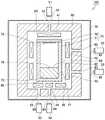
如图21所示,碳化硅单晶锭的制造设备100主要包含:坩埚74、隔热体60、炉体76、第一加热器41、第二加热器42、第三加热器43、第四加热器44、第五加热器45、第一辐射温度计51、第二辐射温度计52、第三辐射温度计53、第四辐射温度计54和第五辐射温度计55。坩埚74具有晶种保持部70和源材料容纳部71。将第一加热器41、第二加热器42、第三加热器43、第四加热器44和第五加热器45设置在隔热体60的内部。隔热体60设置在炉体76的内部。第一辐射温度计51、第二辐射温度计52、第三辐射温度计53、第四辐射温度计54和第五辐射温度计55设置在炉体76的外部。As shown in FIG. 21 , the silicon carbide single crystal
隔热体60具有第一通孔61、第二通孔62、第三通孔63,第四通孔64和第五通孔65。第一辐射温度计51设置在面对坩埚74的顶面83的位置处,并且以经由第一窗口91测量顶面83的中心附近的温度的方式构造。第二辐射温度计52设置在面对坩埚74的侧面84的上部的位置处,并且以经由第二窗口92测量侧面84上部的温度的方式构造。第三辐射温度计53设置在面对坩埚74的侧面84的下部的位置处,并且以经由第三窗口93测量侧面84下部的温度的方式构造。第四辐射温度计54设置在面对坩埚74的底面85的位置处,并且以经由第四窗口94测量底面85的中心附近的温度的方式构造。第五辐射温度计55设置在面对坩埚74的底面85的位置处,并且以经由第五窗口95测量底面85外部的温度的方式构造。The
例如,由第三辐射温度计53测量的控制点77是坩埚74的侧面84的一部分。控制点77的温度由第三辐射温度计53测量,且第三加热器43受到反馈控制。控制点77可以不是坩埚74。控制点77例如可以是加热器的一部分。类似地,对于各个其他加热器,控制点的温度由相应的辐射温度计测量并被反馈回加热器。可以提供与加热器的数量相同的控制点数量,并且加热器可以根据相应的控制点单独进行反馈控制。可以通过主-从控制来控制加热器,其中确定主加热器并且部分加热器以相对于主加热器的输出提供特定比例的输出。多个主加热器可以设置在主-从控制器中。在时间轴上,反馈控制和主-从控制可以组合。For example, the
源材料容纳部71以容纳碳化硅原料73的方式构造。籽晶保持部70以保持由碳化硅单晶构成的籽晶72的方式构造。例如,第一~第五加热器41~45中的每一个是电阻加热型加热器。例如,第一~第五加热器41~45中的每一个可以是高频感应加热型线圈。The source
接着,下面对用于制造碳化硅单晶衬底的方法进行说明。Next, a method for manufacturing a silicon carbide single crystal substrate will be described below.
如图21所示,碳化硅源材料73设置在源材料容纳部71内。碳化硅源材料73例如是多晶碳化硅粉末。例如,使用胶粘剂将籽晶72固定到籽晶保持部70。籽晶72例如由多型4H的六方晶系碳化硅单晶构成。籽晶72的表面直径例如大于或等于100mm,优选大于或等于150mm。例如,籽晶72的表面对应于相对于(0001)面倾斜大于或等于0.5°并且小于或等于8°的面。籽晶72以面对碳化硅源材料73的表面82的方式设置。如上所述,籽晶72和碳化硅源材料73设置在坩埚74中。As shown in FIG. 21 , silicon
接着,例如,将坩埚74加热直至约大于或等于2000℃且小于或等于2400℃的温度。例如,在提高坩埚74的温度的同时,将炉体76内的气氛气体的压力保持在约80kPa下。例如,所述气氛气体包括惰性气体如氩气、氦气或氮气。接着,将炉体76内的气氛气体的压力例如降低至1.7kPa。由此,碳化硅源材料73开始升华,并且在设置在面对碳化硅源材料73表面的位置处的籽晶72的表面上重结晶。结果,碳化硅单晶开始在籽晶72的表面上生长。在碳化硅单晶生长期间,炉体76中的压力例如保持在约大于或等于0.5kPa并且小于或等于5kPa下并持续约100小时。通过如上所述使碳化硅源材料73升华,在籽晶72上生长碳化硅单晶80(参考图22)。Next, for example, the
在生长碳化硅单晶的步骤中,碳化硅单晶80的表面81(参见图22)的温度保持为低于碳化硅源材料73的表面82(参见图22)的温度。具体地,在从碳化硅源材料73朝向籽晶72的方向上,提供温度梯度,使得碳化硅单晶体80的表面81的温度变得低于碳化硅源材料73的表面82的温度。In the step of growing the silicon carbide single crystal, the temperature of the surface 81 (see FIG. 22 ) of the silicon carbide
如上所述,为了得到具有小应变的高质量碳化硅单晶,期望的是,在生长碳化硅单晶过程中在晶体表面的热环境变化小的条件下实施碳化硅单晶80的生长,同时保持碳化硅单晶80的生长表面81尽可能平坦。具体地,在生长碳化硅单晶的步骤中,碳化硅单晶80的生长表面81的温度分布(即,生长表面81中的最高温度与最低温度之差)保持为始终小于或等于5℃。在生长碳化硅单晶的步骤中,生长表面81的中心79的温度(即在从开始生长碳化硅单晶80到停止生长碳化硅单晶80的时间段期间生长表面81的中心79的最高温度与最低温度之差)保持为始终小于或等于3℃。As described above, in order to obtain a high-quality silicon carbide single crystal with a small strain, it is desirable to carry out the growth of the silicon carbide
在生长碳化硅单晶的步骤中,碳化硅源材料73的温度分布(即整个碳化硅源材料中的最高温度与最低温度之差)保持为始终小于或等于20℃。在生长碳化硅单晶的步骤中,碳化硅源材料73的表面82的中心78的温度(即在从开始生长碳化硅单晶80到停止生长碳化硅单晶80的时间段期间表面82的中心78的最高温度与最低温度之差)保持为始终小于或等于5℃。In the step of growing the silicon carbide single crystal, the temperature distribution of the silicon carbide source material 73 (ie, the difference between the highest temperature and the lowest temperature in the entire silicon carbide source material) is kept to be less than or equal to 20° C. at all times. In the step of growing the silicon carbide single crystal, the temperature of the
在生长碳化硅单晶的步骤中,为了实现上述条件,通过热流体模拟来计算第一加热器41~第五加热器45的加热器功率的最佳值。具体地,在其中碳化硅单晶的长度为0~25mm的范围内,每1mm实施热流体模拟,由此计算第一加热器41~第五加热器45的加热器功率的最佳值。In the step of growing a silicon carbide single crystal, in order to realize the above-mentioned conditions, the optimum values of the heater powers of the
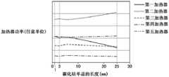
接着,对在生长碳化硅单晶的步骤中第一加热器~第五加热器的加热器功率的示例性最佳值进行说明。在图23中,纵轴代表第一加热器41~第五加热器45的每个加热器的功率,而横轴代表在籽晶72上生长的碳化硅单晶80的长度113(参见图22)。换言之,横轴对应于生长时间。Next, an exemplary optimum value of the heater powers of the first heater to the fifth heater in the step of growing a silicon carbide single crystal will be described. In FIG. 23, the vertical axis represents the power of each heater of the
如图23所示,当碳化硅单晶的长度为1mm(在开始生长碳化硅单晶之后即刻)时,在五个加热器中,第二加热器42的加热器功率最大且第四加热器44的加热器功率最小。第一加热器41和第五加热器45的加热器功率大于第三加热器43的加热器功率。第一加热器41的加热器功率与第五加热器45的加热器功率基本相同。As shown in FIG. 23, when the length of the silicon carbide single crystal is 1 mm (immediately after the start of growth of the silicon carbide single crystal), among the five heaters, the heater power of the
在碳化硅单晶的长度为1mm~3mm时,第二加热器42的加热器功率升高。第一加热器41、第三加热器43和第四加热器44的加热器功率减小。在碳化硅单晶的长度变为约3mm之后,第二加热器42和第五加热器45的加热器功率减小。然后,第二加热器42的加热器功率升高。在碳化硅单晶的长度变为约3mm之后,第一加热器41、第三加热器43和第四加热器44的加热器功率暂时升高。然后,第一加热器41、第三加热器43和第四加热器44的加热器功率减小。When the length of the silicon carbide single crystal is 1 mm to 3 mm, the heater power of the
如图23所示,当碳化硅单晶的长度由于碳化硅单晶的生长而变为约3mm时,第一加热器41的加热器功率暂时增加,但是然后逐渐减小。另一方面,当碳化硅单晶的长度由于碳化硅单晶的生长而变为约3mm时,第二加热器42的加热器功率暂时降低,但是然后逐渐增加。当碳化硅单晶的长度为25mm时(在碳化硅单晶生长结束时),在五个加热器中,第二加热器42的加热器功率最大,且第四加热器44的加热器功率最小。第五加热器45的加热器功率大于第三加热器43的加热器功率。第一加热器41的加热器功率小于第三加热器43的加热器功率。As shown in FIG. 23 , when the length of the silicon carbide single crystal became about 3 mm due to the growth of the silicon carbide single crystal, the heater power of the
在碳化硅单晶80的结晶生长结束之后,将碳化硅单晶80冷却。在碳化硅单晶80的温度变为约室温之后,将碳化硅单晶80从制造设备100移出。使用例如线锯将碳化硅单晶80切片,从而得到碳化硅单晶衬底10(参见图1)。After the crystal growth of silicon carbide
在上述实施方案中,已经显示,能够单独控制加热器功率的加热器的区域的数量是5;然而,所述区域的数量不限于5。例如,通过进一步划分顶面侧加热器、侧面侧加热器和底面侧加热器,所述加热器的区域的数量可以是6、7或8。通过增加加热器的区域的数量,能够精确控制碳化硅单晶的温度。因此,能够得到应变进一步降低的碳化硅单晶衬底。In the above-described embodiment, it has been shown that the number of zones of the heater capable of individually controlling heater power is five; however, the number of zones is not limited to five. For example, the number of regions of the heater may be 6, 7, or 8 by further dividing the top surface side heater, the side surface side heater, and the bottom surface side heater. By increasing the number of regions of the heater, the temperature of the silicon carbide single crystal can be precisely controlled. Therefore, a silicon carbide single crystal substrate with further reduced strain can be obtained.
本文中公开的实施方案在任何方面都是示例性的而非限制性的。本发明的范围由权利要求书的条款限定,而不是由上述实施方案限定,并且旨在包括与权利要求书的条款等同的范围和含义内的任何修改。The embodiments disclosed herein are illustrative and not restrictive in any respect. The scope of the present invention is defined by the terms of the claims, rather than the above-described embodiments, and is intended to include any modifications within the scope and meaning equivalent to the terms of the claims.
附图标记说明Explanation of reference signs
1:第一强度分布;2:第二强度分布;3:第三强度分布;4:第四强度分布;5:X射线发射器;6:检测器;7:入射X射线(X射线);8:衍射X射线;10:碳化硅单晶衬底;11:第一主面(主面);12:第二主面;13:第一平坦部;14:弯曲部;15:外边缘;16:最大直径;31:第一测量区域;32:第二测量区域;41:第一加热器;42:第二加热器;43:第三加热器;44:第四加热器;45:第五加热器;51:第一辐射温度计;52:第二辐射温度计;53:第三辐射温度计;54:第四辐射温度计;55:第五辐射温度计;60:隔热体;61:第一通孔;62:第二通孔;63:第三通孔;64:第四通孔;65:第五通孔;70:籽晶保持部;71:源材料容纳部;72:籽晶;73:碳化硅源材料;74:坩埚;76:炉体;77:控制点;78、79、O:中心;80:碳化硅单晶;81:生长表面(表面);82:表面;83:顶面;84:侧面;85:底面;91:第一窗口;92:第二窗口;93:第三窗口;94:第四窗口;95:第五个窗口;100:制造设备;101:第一方向(偏离方向);102:第二方向;111、112:差异;113:长度;E1:第一能量;E2:第二能量;E3:第三能源;E4:第四能量;EH1、EH2:最大值;EL1、EL2:最小值;IN1、IN2、IN3、IN4:背景强度;IP1、IP2、IP3、IP4:最大强度。1: first intensity distribution; 2: second intensity distribution; 3: third intensity distribution; 4: fourth intensity distribution; 5: X-ray emitter; 6: detector; 7: incident X-ray (X-ray); 8: diffracted X-ray; 10: silicon carbide single crystal substrate; 11: first main surface (main surface); 12: second main surface; 13: first flat part; 14: curved part; 15: outer edge; 16: maximum diameter; 31: first measurement area; 32: second measurement area; 41: first heater; 42: second heater; 43: third heater; 44: fourth heater; 45: first Five heaters; 51: first radiation thermometer; 52: second radiation thermometer; 53: third radiation thermometer; 54: fourth radiation thermometer; 55: fifth radiation thermometer; 60: heat insulator; 61: first pass Hole; 62: second through hole; 63: third through hole; 64: fourth through hole; 65: fifth through hole; 70: seed crystal holding portion; 71: source material accommodation portion; 72: seed crystal; 73 : SiC source material; 74: crucible; 76: furnace body; 77: control point; 78, 79, O: center; 80: SiC single crystal; 81: growth surface (surface); 82: surface; 83: top surface; 84: side; 85: bottom; 91: first window; 92: second window; 93: third window; 94: fourth window; 95: fifth window; 100: manufacturing equipment; 101: first Direction (deviation direction); 102: second direction; 111, 112: difference; 113: length; E1: first energy; E2: second energy; E3: third energy; E4: fourth energy; EH1, EH2: Maximum value; EL1, EL2: minimum value; IN1, IN2, IN3, IN4: background intensity; IP1, IP2, IP3, IP4: maximum intensity.
Claims (4)
Applications Claiming Priority (3)
| Application Number | Priority Date | Filing Date | Title |
|---|---|---|---|
| JP2016-022388 | 2016-02-09 | ||
| JP2016022388 | 2016-02-09 | ||
| PCT/JP2017/003139WO2017138383A1 (en) | 2016-02-09 | 2017-01-30 | Silicon carbide single crystal substrate |
Publications (2)
| Publication Number | Publication Date |
|---|---|
| CN108495957A CN108495957A (en) | 2018-09-04 |
| CN108495957Btrue CN108495957B (en) | 2022-11-25 |
Family
ID=59563258
Family Applications (1)
| Application Number | Title | Priority Date | Filing Date |
|---|---|---|---|
| CN201780007967.4AActiveCN108495957B (en) | 2016-02-09 | 2017-01-30 | SiC single crystal substrate |
Country Status (5)
| Country | Link |
|---|---|
| US (2) | US11535953B2 (en) |
| JP (2) | JP6729605B2 (en) |
| CN (1) | CN108495957B (en) |
| DE (1) | DE112017000725T5 (en) |
| WO (1) | WO2017138383A1 (en) |
Families Citing this family (6)
| Publication number | Priority date | Publication date | Assignee | Title |
|---|---|---|---|---|
| CN108495957B (en)* | 2016-02-09 | 2022-11-25 | 住友电气工业株式会社 | SiC single crystal substrate |
| CN108493292B (en)* | 2018-04-12 | 2020-06-09 | 大连理工大学 | Silicon carbide single crystal-based X-ray detector and preparation method thereof |
| CN112176396A (en)* | 2020-09-22 | 2021-01-05 | 南京晶升能源设备有限公司 | Axial temperature multi-gradient controllable thermal field and crystal growth furnace |
| JP7643708B2 (en)* | 2020-09-28 | 2025-03-11 | Secカーボン株式会社 | SiC single crystal growth equipment |
| CN114481324A (en)* | 2022-01-25 | 2022-05-13 | 北京北方华创微电子装备有限公司 | Semiconductor processing apparatus and heating method for target growth |
| WO2024225767A1 (en)* | 2023-04-26 | 2024-10-31 | 에스케이실트론 주식회사 | Wafer and shape analysis method therefor |
Citations (3)
| Publication number | Priority date | Publication date | Assignee | Title |
|---|---|---|---|---|
| JP2008290898A (en)* | 2007-05-23 | 2008-12-04 | Nippon Steel Corp | Low resistivity silicon carbide single crystal substrate |
| JP2013089937A (en)* | 2011-10-24 | 2013-05-13 | Sumitomo Electric Ind Ltd | Method of manufacturing silicon carbide substrate, and silicon carbide substrate |
| CN103476975A (en)* | 2011-05-20 | 2013-12-25 | 住友电气工业株式会社 | Silicon carbide substrate, silicon carbide ingot and manufacturing methods therefor |
Family Cites Families (10)
| Publication number | Priority date | Publication date | Assignee | Title |
|---|---|---|---|---|
| DE10247017B4 (en)* | 2001-10-12 | 2009-06-10 | Denso Corp., Kariya-shi | SiC single crystal, a method of producing a SiC single crystal, SiC wafers with an epitaxial film, and a method of producing a SiC wafer having an epitaxial film |
| US7422634B2 (en) | 2005-04-07 | 2008-09-09 | Cree, Inc. | Three inch silicon carbide wafer with low warp, bow, and TTV |
| JP4877204B2 (en) | 2007-11-13 | 2012-02-15 | 株式会社デンソー | Silicon carbide single crystal manufacturing equipment |
| JP2011219322A (en)* | 2010-04-12 | 2011-11-04 | Sumitomo Electric Ind Ltd | Silicon carbide substrate |
| JP5189156B2 (en)* | 2010-11-29 | 2013-04-24 | 株式会社豊田中央研究所 | Method for producing SiC single crystal |
| JP6025306B2 (en)* | 2011-05-16 | 2016-11-16 | 株式会社豊田中央研究所 | SiC single crystal, SiC wafer and semiconductor device |
| WO2013031856A1 (en)* | 2011-08-29 | 2013-03-07 | 新日鐵住金株式会社 | Silicon carbide single crystal wafer and manufacturing method for same |
| JP6124287B2 (en) | 2013-03-04 | 2017-05-10 | 一般財団法人電力中央研究所 | Method for inspecting silicon carbide substrate or silicon carbide semiconductor element, and method for manufacturing silicon carbide substrate or silicon carbide semiconductor element |
| CN108495957B (en)* | 2016-02-09 | 2022-11-25 | 住友电气工业株式会社 | SiC single crystal substrate |
| JP6762484B2 (en)* | 2017-01-10 | 2020-09-30 | 昭和電工株式会社 | SiC epitaxial wafer and its manufacturing method |
- 2017
- 2017-01-30CNCN201780007967.4Apatent/CN108495957B/enactiveActive
- 2017-01-30USUS16/074,143patent/US11535953B2/enactiveActive
- 2017-01-30DEDE112017000725.9Tpatent/DE112017000725T5/enactivePending
- 2017-01-30JPJP2017566583Apatent/JP6729605B2/enactiveActive
- 2017-01-30WOPCT/JP2017/003139patent/WO2017138383A1/ennot_activeCeased
- 2020
- 2020-06-30JPJP2020112619Apatent/JP6969635B2/enactiveActive
- 2022
- 2022-11-23USUS17/993,200patent/US11781246B2/enactiveActive
Patent Citations (3)
| Publication number | Priority date | Publication date | Assignee | Title |
|---|---|---|---|---|
| JP2008290898A (en)* | 2007-05-23 | 2008-12-04 | Nippon Steel Corp | Low resistivity silicon carbide single crystal substrate |
| CN103476975A (en)* | 2011-05-20 | 2013-12-25 | 住友电气工业株式会社 | Silicon carbide substrate, silicon carbide ingot and manufacturing methods therefor |
| JP2013089937A (en)* | 2011-10-24 | 2013-05-13 | Sumitomo Electric Ind Ltd | Method of manufacturing silicon carbide substrate, and silicon carbide substrate |
Also Published As
| Publication number | Publication date |
|---|---|
| US11781246B2 (en) | 2023-10-10 |
| US20230081506A1 (en) | 2023-03-16 |
| JPWO2017138383A1 (en) | 2018-11-29 |
| CN108495957A (en) | 2018-09-04 |
| WO2017138383A1 (en) | 2017-08-17 |
| US11535953B2 (en) | 2022-12-27 |
| DE112017000725T5 (en) | 2018-10-31 |
| US20210054529A1 (en) | 2021-02-25 |
| JP6729605B2 (en) | 2020-07-22 |
| JP6969635B2 (en) | 2021-11-24 |
| JP2020172433A (en) | 2020-10-22 |
Similar Documents
| Publication | Publication Date | Title |
|---|---|---|
| CN108495957B (en) | SiC single crystal substrate | |
| JP4388538B2 (en) | Silicon carbide single crystal manufacturing equipment | |
| KR101823216B1 (en) | Silicon carbide single crystal wafer and method of manufacturing a silicon carbide single crystal ingot | |
| EP3396029B1 (en) | Sic single crystal production method and production apparatus | |
| CN107223168B (en) | Furnace for seed sublimation of wide bandgap crystals | |
| CN106637411B (en) | A kind of aluminum-nitride single crystal growing method | |
| WO2016152813A1 (en) | Method for producing silicon carbide single crystal | |
| TWI677602B (en) | β-GaZO single crystal substrate | |
| JP2021066650A (en) | Silicon carbide ingot, method for manufacturing the same and method for manufacturing silicon carbide wafer | |
| US20230160103A1 (en) | Silicon carbide single crystal and method of manufacturing silicon carbide single crystal | |
| CN114423889B (en) | Method for producing SiC single crystal, apparatus for producing SiC single crystal, and SiC single crystal wafer | |
| JP6869077B2 (en) | Method for manufacturing silicon carbide single crystal ingot | |
| US20160155808A1 (en) | Method of manufacturing silicon carbide single crystal and silicon carbide single crystal substrate | |
| JP2017095319A (en) | Method for producing SiC single crystal ingot, SiC single crystal ingot, and SiC single crystal wafer | |
| KR20100130939A (en) | Manufacturing apparatus and manufacturing method of compound semiconductor single crystal | |
| US12325934B2 (en) | Single-crystal silicon carbide wafer, and single-crystal silicon carbide ingot | |
| Shengurov et al. | A silicon sublimation source for molecular-beam epitaxy | |
| JP2017206408A (en) | Production of silicon carbide monocrystal | |
| JP2016088805A (en) | Silicon carbide single crystal manufacturing apparatus and silicon carbide single crystal manufacturing method | |
| Lee et al. | The role of air-pocket in crucible structure for high quality SiC crystal growth | |
| EP3243935A1 (en) | Sic single crystal and method for producing same | |
| Kravtsov | Ingots pulled with electron beam heating from skull-a new feedstock for fz crystals applicable for solar cells | |
| JP6860054B2 (en) | Method for producing silicon carbide single crystal | |
| Safronov et al. | Manufacture of sapphire ribbons with low dislocation density | |
| Dhanaraj et al. | PVT growth of 6H SiC crystals and defect characterization |
Legal Events
| Date | Code | Title | Description |
|---|---|---|---|
| PB01 | Publication | ||
| PB01 | Publication | ||
| SE01 | Entry into force of request for substantive examination | ||
| SE01 | Entry into force of request for substantive examination | ||
| GR01 | Patent grant | ||
| GR01 | Patent grant |