CN108493201B - A display panel, its manufacturing method and display device - Google Patents
A display panel, its manufacturing method and display deviceDownload PDFInfo
- Publication number
- CN108493201B CN108493201BCN201810201260.3ACN201810201260ACN108493201BCN 108493201 BCN108493201 BCN 108493201BCN 201810201260 ACN201810201260 ACN 201810201260ACN 108493201 BCN108493201 BCN 108493201B
- Authority
- CN
- China
- Prior art keywords
- type semiconductor
- semiconductor layer
- light
- fingerprint identification
- layer
- Prior art date
- Legal status (The legal status is an assumption and is not a legal conclusion. Google has not performed a legal analysis and makes no representation as to the accuracy of the status listed.)
- Active
Links
Images


Classifications
- H—ELECTRICITY
- H10—SEMICONDUCTOR DEVICES; ELECTRIC SOLID-STATE DEVICES NOT OTHERWISE PROVIDED FOR
- H10F—INORGANIC SEMICONDUCTOR DEVICES SENSITIVE TO INFRARED RADIATION, LIGHT, ELECTROMAGNETIC RADIATION OF SHORTER WAVELENGTH OR CORPUSCULAR RADIATION
- H10F39/00—Integrated devices, or assemblies of multiple devices, comprising at least one element covered by group H10F30/00, e.g. radiation detectors comprising photodiode arrays
- H10F39/10—Integrated devices
- H10F39/12—Image sensors
- H10F39/198—Contact-type image sensors [CIS]
- H—ELECTRICITY
- H10—SEMICONDUCTOR DEVICES; ELECTRIC SOLID-STATE DEVICES NOT OTHERWISE PROVIDED FOR
- H10F—INORGANIC SEMICONDUCTOR DEVICES SENSITIVE TO INFRARED RADIATION, LIGHT, ELECTROMAGNETIC RADIATION OF SHORTER WAVELENGTH OR CORPUSCULAR RADIATION
- H10F39/00—Integrated devices, or assemblies of multiple devices, comprising at least one element covered by group H10F30/00, e.g. radiation detectors comprising photodiode arrays
- H10F39/10—Integrated devices
- H10F39/103—Integrated devices the at least one element covered by H10F30/00 having potential barriers, e.g. integrated devices comprising photodiodes or phototransistors
- G—PHYSICS
- G06—COMPUTING OR CALCULATING; COUNTING
- G06F—ELECTRIC DIGITAL DATA PROCESSING
- G06F3/00—Input arrangements for transferring data to be processed into a form capable of being handled by the computer; Output arrangements for transferring data from processing unit to output unit, e.g. interface arrangements
- G06F3/01—Input arrangements or combined input and output arrangements for interaction between user and computer
- G06F3/03—Arrangements for converting the position or the displacement of a member into a coded form
- G06F3/041—Digitisers, e.g. for touch screens or touch pads, characterised by the transducing means
- G06F3/0412—Digitisers structurally integrated in a display
- G—PHYSICS
- G06—COMPUTING OR CALCULATING; COUNTING
- G06V—IMAGE OR VIDEO RECOGNITION OR UNDERSTANDING
- G06V40/00—Recognition of biometric, human-related or animal-related patterns in image or video data
- G06V40/10—Human or animal bodies, e.g. vehicle occupants or pedestrians; Body parts, e.g. hands
- G06V40/12—Fingerprints or palmprints
- G06V40/13—Sensors therefor
- G06V40/1318—Sensors therefor using electro-optical elements or layers, e.g. electroluminescent sensing
- H—ELECTRICITY
- H01—ELECTRIC ELEMENTS
- H01L—SEMICONDUCTOR DEVICES NOT COVERED BY CLASS H10
- H01L25/00—Assemblies consisting of a plurality of semiconductor or other solid state devices
- H01L25/16—Assemblies consisting of a plurality of semiconductor or other solid state devices the devices being of types provided for in two or more different subclasses of H10B, H10D, H10F, H10H, H10K or H10N, e.g. forming hybrid circuits
- H01L25/167—Assemblies consisting of a plurality of semiconductor or other solid state devices the devices being of types provided for in two or more different subclasses of H10B, H10D, H10F, H10H, H10K or H10N, e.g. forming hybrid circuits comprising optoelectronic devices, e.g. LED, photodiodes
- H—ELECTRICITY
- H10—SEMICONDUCTOR DEVICES; ELECTRIC SOLID-STATE DEVICES NOT OTHERWISE PROVIDED FOR
- H10F—INORGANIC SEMICONDUCTOR DEVICES SENSITIVE TO INFRARED RADIATION, LIGHT, ELECTROMAGNETIC RADIATION OF SHORTER WAVELENGTH OR CORPUSCULAR RADIATION
- H10F39/00—Integrated devices, or assemblies of multiple devices, comprising at least one element covered by group H10F30/00, e.g. radiation detectors comprising photodiode arrays
- H10F39/011—Manufacture or treatment of image sensors covered by group H10F39/12
- H10F39/024—Manufacture or treatment of image sensors covered by group H10F39/12 of coatings or optical elements
- H—ELECTRICITY
- H10—SEMICONDUCTOR DEVICES; ELECTRIC SOLID-STATE DEVICES NOT OTHERWISE PROVIDED FOR
- H10F—INORGANIC SEMICONDUCTOR DEVICES SENSITIVE TO INFRARED RADIATION, LIGHT, ELECTROMAGNETIC RADIATION OF SHORTER WAVELENGTH OR CORPUSCULAR RADIATION
- H10F39/00—Integrated devices, or assemblies of multiple devices, comprising at least one element covered by group H10F30/00, e.g. radiation detectors comprising photodiode arrays
- H10F39/10—Integrated devices
- H10F39/107—Integrated devices having multiple elements covered by H10F30/00 in a repetitive configuration, e.g. radiation detectors comprising photodiode arrays
- H—ELECTRICITY
- H10—SEMICONDUCTOR DEVICES; ELECTRIC SOLID-STATE DEVICES NOT OTHERWISE PROVIDED FOR
- H10F—INORGANIC SEMICONDUCTOR DEVICES SENSITIVE TO INFRARED RADIATION, LIGHT, ELECTROMAGNETIC RADIATION OF SHORTER WAVELENGTH OR CORPUSCULAR RADIATION
- H10F39/00—Integrated devices, or assemblies of multiple devices, comprising at least one element covered by group H10F30/00, e.g. radiation detectors comprising photodiode arrays
- H10F39/80—Constructional details of image sensors
- H10F39/805—Coatings
- H10F39/8057—Optical shielding
- H—ELECTRICITY
- H10—SEMICONDUCTOR DEVICES; ELECTRIC SOLID-STATE DEVICES NOT OTHERWISE PROVIDED FOR
- H10H—INORGANIC LIGHT-EMITTING SEMICONDUCTOR DEVICES HAVING POTENTIAL BARRIERS
- H10H20/00—Individual inorganic light-emitting semiconductor devices having potential barriers, e.g. light-emitting diodes [LED]
- H10H20/01—Manufacture or treatment
- H—ELECTRICITY
- H10—SEMICONDUCTOR DEVICES; ELECTRIC SOLID-STATE DEVICES NOT OTHERWISE PROVIDED FOR
- H10H—INORGANIC LIGHT-EMITTING SEMICONDUCTOR DEVICES HAVING POTENTIAL BARRIERS
- H10H29/00—Integrated devices, or assemblies of multiple devices, comprising at least one light-emitting semiconductor element covered by group H10H20/00
- H10H29/10—Integrated devices comprising at least one light-emitting semiconductor component covered by group H10H20/00
- H10H29/14—Integrated devices comprising at least one light-emitting semiconductor component covered by group H10H20/00 comprising multiple light-emitting semiconductor components
- H10H29/142—Two-dimensional arrangements, e.g. asymmetric LED layout
- G—PHYSICS
- G06—COMPUTING OR CALCULATING; COUNTING
- G06F—ELECTRIC DIGITAL DATA PROCESSING
- G06F2203/00—Indexing scheme relating to G06F3/00 - G06F3/048
- G06F2203/041—Indexing scheme relating to G06F3/041 - G06F3/045
- G06F2203/04103—Manufacturing, i.e. details related to manufacturing processes specially suited for touch sensitive devices
- H—ELECTRICITY
- H01—ELECTRIC ELEMENTS
- H01L—SEMICONDUCTOR DEVICES NOT COVERED BY CLASS H10
- H01L25/00—Assemblies consisting of a plurality of semiconductor or other solid state devices
- H01L25/03—Assemblies consisting of a plurality of semiconductor or other solid state devices all the devices being of a type provided for in a single subclass of subclasses H10B, H10D, H10F, H10H, H10K or H10N, e.g. assemblies of rectifier diodes
- H01L25/04—Assemblies consisting of a plurality of semiconductor or other solid state devices all the devices being of a type provided for in a single subclass of subclasses H10B, H10D, H10F, H10H, H10K or H10N, e.g. assemblies of rectifier diodes the devices not having separate containers
- H01L25/075—Assemblies consisting of a plurality of semiconductor or other solid state devices all the devices being of a type provided for in a single subclass of subclasses H10B, H10D, H10F, H10H, H10K or H10N, e.g. assemblies of rectifier diodes the devices not having separate containers the devices being of a type provided for in group H10H20/00
- H01L25/0753—Assemblies consisting of a plurality of semiconductor or other solid state devices all the devices being of a type provided for in a single subclass of subclasses H10B, H10D, H10F, H10H, H10K or H10N, e.g. assemblies of rectifier diodes the devices not having separate containers the devices being of a type provided for in group H10H20/00 the devices being arranged next to each other
- H—ELECTRICITY
- H10—SEMICONDUCTOR DEVICES; ELECTRIC SOLID-STATE DEVICES NOT OTHERWISE PROVIDED FOR
- H10F—INORGANIC SEMICONDUCTOR DEVICES SENSITIVE TO INFRARED RADIATION, LIGHT, ELECTROMAGNETIC RADIATION OF SHORTER WAVELENGTH OR CORPUSCULAR RADIATION
- H10F55/00—Radiation-sensitive semiconductor devices covered by groups H10F10/00, H10F19/00 or H10F30/00 being structurally associated with electric light sources and electrically or optically coupled thereto
- H10F55/18—Radiation-sensitive semiconductor devices covered by groups H10F10/00, H10F19/00 or H10F30/00 being structurally associated with electric light sources and electrically or optically coupled thereto wherein the radiation-sensitive semiconductor devices and the electric light source share a common body having dual-functionality of light emission and light detection
- H—ELECTRICITY
- H10—SEMICONDUCTOR DEVICES; ELECTRIC SOLID-STATE DEVICES NOT OTHERWISE PROVIDED FOR
- H10F—INORGANIC SEMICONDUCTOR DEVICES SENSITIVE TO INFRARED RADIATION, LIGHT, ELECTROMAGNETIC RADIATION OF SHORTER WAVELENGTH OR CORPUSCULAR RADIATION
- H10F77/00—Constructional details of devices covered by this subclass
- H10F77/20—Electrodes
- H10F77/206—Electrodes for devices having potential barriers
- H—ELECTRICITY
- H10—SEMICONDUCTOR DEVICES; ELECTRIC SOLID-STATE DEVICES NOT OTHERWISE PROVIDED FOR
- H10H—INORGANIC LIGHT-EMITTING SEMICONDUCTOR DEVICES HAVING POTENTIAL BARRIERS
- H10H20/00—Individual inorganic light-emitting semiconductor devices having potential barriers, e.g. light-emitting diodes [LED]
- H10H20/01—Manufacture or treatment
- H10H20/011—Manufacture or treatment of bodies, e.g. forming semiconductor layers
- H10H20/018—Bonding of wafers
- H—ELECTRICITY
- H10—SEMICONDUCTOR DEVICES; ELECTRIC SOLID-STATE DEVICES NOT OTHERWISE PROVIDED FOR
- H10H—INORGANIC LIGHT-EMITTING SEMICONDUCTOR DEVICES HAVING POTENTIAL BARRIERS
- H10H20/00—Individual inorganic light-emitting semiconductor devices having potential barriers, e.g. light-emitting diodes [LED]
- H10H20/01—Manufacture or treatment
- H10H20/032—Manufacture or treatment of electrodes
- H—ELECTRICITY
- H10—SEMICONDUCTOR DEVICES; ELECTRIC SOLID-STATE DEVICES NOT OTHERWISE PROVIDED FOR
- H10H—INORGANIC LIGHT-EMITTING SEMICONDUCTOR DEVICES HAVING POTENTIAL BARRIERS
- H10H20/00—Individual inorganic light-emitting semiconductor devices having potential barriers, e.g. light-emitting diodes [LED]
- H10H20/80—Constructional details
- H10H20/81—Bodies
- H10H20/814—Bodies having reflecting means, e.g. semiconductor Bragg reflectors
- H10H20/8142—Bodies having reflecting means, e.g. semiconductor Bragg reflectors forming resonant cavity structures
- H—ELECTRICITY
- H10—SEMICONDUCTOR DEVICES; ELECTRIC SOLID-STATE DEVICES NOT OTHERWISE PROVIDED FOR
- H10H—INORGANIC LIGHT-EMITTING SEMICONDUCTOR DEVICES HAVING POTENTIAL BARRIERS
- H10H20/00—Individual inorganic light-emitting semiconductor devices having potential barriers, e.g. light-emitting diodes [LED]
- H10H20/80—Constructional details
- H10H20/83—Electrodes
- H—ELECTRICITY
- H10—SEMICONDUCTOR DEVICES; ELECTRIC SOLID-STATE DEVICES NOT OTHERWISE PROVIDED FOR
- H10H—INORGANIC LIGHT-EMITTING SEMICONDUCTOR DEVICES HAVING POTENTIAL BARRIERS
- H10H20/00—Individual inorganic light-emitting semiconductor devices having potential barriers, e.g. light-emitting diodes [LED]
- H10H20/80—Constructional details
- H10H20/85—Packages
Landscapes
- Engineering & Computer Science (AREA)
- Theoretical Computer Science (AREA)
- General Physics & Mathematics (AREA)
- Physics & Mathematics (AREA)
- Human Computer Interaction (AREA)
- Microelectronics & Electronic Packaging (AREA)
- General Engineering & Computer Science (AREA)
- Multimedia (AREA)
- Condensed Matter Physics & Semiconductors (AREA)
- Computer Hardware Design (AREA)
- Power Engineering (AREA)
- Electroluminescent Light Sources (AREA)
- Devices For Indicating Variable Information By Combining Individual Elements (AREA)
Abstract
Translated fromChinese
Description
Translated fromChinese技术领域technical field
本发明涉及显示技术,尤其涉及一种显示面板、其制造方法及显示装置。The present invention relates to display technology, and in particular, to a display panel, a manufacturing method thereof and a display device.
背景技术Background technique
每个人包括指纹在内的皮肤纹路在图案、断点和交叉点上各不相同,呈现唯一性且终生不变。据此,我们可以把一个人同他的指纹对应起来,通过将他的指纹和预先保存的指纹数据进行比较,以验证他的真实身份,这就是指纹识别技术。得益于电子集成制造技术和快速而可靠的算法研究,指纹识别技术中光学指纹识别技术已经开始走入我们的日常生活,成为目前生物检测学中研究最深入,应用最广泛,发展最成熟的技术。Each person's skin patterns, including fingerprints, are different in patterns, breakpoints and intersections, which are unique and unchanged for life. Accordingly, we can match a person with his fingerprints, and verify his true identity by comparing his fingerprints with the pre-stored fingerprint data, which is fingerprint identification technology. Thanks to electronic integrated manufacturing technology and fast and reliable algorithm research, optical fingerprint identification technology in fingerprint identification technology has begun to enter our daily life, becoming the most in-depth research, the most widely used and the most mature development in biological detection. technology.
目前,通常将光学指纹识别技术与显示技术相结合,以使显示面板不仅具有正常的显示功能,还能够进行指纹识别,丰富了显示面板的功能,提高了显示面板的安全性能。为了使得显示面板具有指纹识别功能,通常在现有的显示面板中,设置外挂式的指纹识别单元。该外挂式的指纹识别单元通过光学胶粘结于显示面板的衬底基板上。换言之,现有的显示面板中,发光单元和各指纹识别单元在垂直与第一基板所在平面的方向上依次排列。该类显示面板整体厚度较厚,不利于实现显示面板的轻薄化。At present, the optical fingerprint recognition technology is usually combined with the display technology, so that the display panel not only has a normal display function, but also can perform fingerprint recognition, which enriches the function of the display panel and improves the security performance of the display panel. In order to enable the display panel to have a fingerprint identification function, an externally mounted fingerprint identification unit is usually provided in the existing display panel. The externally mounted fingerprint identification unit is bonded to the base substrate of the display panel through optical glue. In other words, in the existing display panel, the light emitting unit and each fingerprint identification unit are sequentially arranged in a direction perpendicular to the plane where the first substrate is located. The overall thickness of this type of display panel is relatively thick, which is not conducive to realizing the thinning of the display panel.
发明内容SUMMARY OF THE INVENTION
本发明提供一种显示面板、其制造方法及显示装置,以减小显示面板的整体厚度,利于实现显示面板的轻薄化。The present invention provides a display panel, a method for manufacturing the same and a display device, so as to reduce the overall thickness of the display panel and facilitate the realization of lightness and thinness of the display panel.
第一方面,本发明实施例提供了一种显示面板,该显示面板包括:In a first aspect, an embodiment of the present invention provides a display panel, the display panel includes:
相对设置的第一基板和第二基板;a first substrate and a second substrate arranged oppositely;
第一基板靠近第二基板的一侧设置有多个发光单元和多个指纹识别单元,发光单元包括第一N型半导体层和第一P型半导体层,指纹识别单元包括第二N型半导体层和第二P型半导体层,第一N型半导体层和第二N型半导体层同层设置,第一P型半导体层和第二P型半导体层同层设置。The side of the first substrate close to the second substrate is provided with a plurality of light-emitting units and a plurality of fingerprint identification units, the light-emitting unit includes a first N-type semiconductor layer and a first P-type semiconductor layer, and the fingerprint identification unit includes a second N-type semiconductor layer and the second P-type semiconductor layer, the first N-type semiconductor layer and the second N-type semiconductor layer are arranged in the same layer, and the first P-type semiconductor layer and the second P-type semiconductor layer are arranged in the same layer.
第二方面,本发明实施例还提供了一种显示面板的制造方法,该制造方法包括:In a second aspect, an embodiment of the present invention further provides a manufacturing method of a display panel, the manufacturing method comprising:
提供第一基板;providing a first substrate;
在第一基板上形成多个发光单元和多个指纹识别单元,发光单元包括第一N型半导体层和第一P型半导体层,指纹识别单元包括第二N型半导体层和第二P型半导体层,第一N型半导体层和第二N型半导体层为同一膜层形成,第一P型半导体层和第二P型半导体层为同一膜层形成。A plurality of light-emitting units and a plurality of fingerprint identification units are formed on the first substrate, the light-emitting units include a first N-type semiconductor layer and a first P-type semiconductor layer, and the fingerprint identification unit includes a second N-type semiconductor layer and a second P-type semiconductor layer The first N-type semiconductor layer and the second N-type semiconductor layer are formed of the same film layer, and the first P-type semiconductor layer and the second P-type semiconductor layer are formed of the same film layer.
第三方面,本发明实施例还提供了一种显示装置,该显示装置包括第一方面提供的显示面板。In a third aspect, an embodiment of the present invention further provides a display device, where the display device includes the display panel provided in the first aspect.
本发明实施例提供的显示面板,通过设置发光单元包括第一N型半导体层和第一P型半导体层,指纹识别单元包括第二N型半导体层和第二P型半导体层,通过设置第一N型半导体层和第二N型半导体层同层设置,第一P型半导体层和第二P型半导体层同层设置,由此各发光单元和各指纹识别单元在第一基板所在平面上依次排列,而非发光单元和各指纹识别单元在垂直与第一基板所在平面的方向上依次排列,解决了现有的显示面板因采用外挂式的指纹识别单元,显示面板的整体厚度较厚,不利于实现显示面板的轻薄化的问题,实现了减少了显示面板的整体厚度,利于实现显示面板的轻薄化的目的。In the display panel provided by the embodiment of the present invention, the light-emitting unit includes a first N-type semiconductor layer and a first P-type semiconductor layer, and the fingerprint identification unit includes a second N-type semiconductor layer and a second P-type semiconductor layer. The N-type semiconductor layer and the second N-type semiconductor layer are arranged in the same layer, and the first P-type semiconductor layer and the second P-type semiconductor layer are arranged in the same layer, so that each light-emitting unit and each fingerprint identification unit are arranged in sequence on the plane of the first substrate. The non-light-emitting unit and each fingerprint identification unit are arranged in turn in the direction perpendicular to the plane where the first substrate is located, which solves the problem that the existing display panel uses an external fingerprint identification unit, the overall thickness of the display panel is thicker, and the It is beneficial to realize the problem of lightening and thinning of the display panel, realizes the reduction of the overall thickness of the display panel, and is beneficial to realize the purpose of realizing the lightness and thinning of the display panel.
附图说明Description of drawings
图1为现有技术提供的一种显示面板的结构示意图;1 is a schematic structural diagram of a display panel provided by the prior art;
图2为本发明实施例提供的一种显示面板的结构示意图;FIG. 2 is a schematic structural diagram of a display panel according to an embodiment of the present invention;
图3为本发明实施例提供的另一种显示面板的结构示意图;FIG. 3 is a schematic structural diagram of another display panel according to an embodiment of the present invention;
图4为本发明实施例提供的又一种显示面板的结构示意图;FIG. 4 is a schematic structural diagram of another display panel according to an embodiment of the present invention;
图5为本发明实施例提供的一种驱动周期的示意图;FIG. 5 is a schematic diagram of a driving cycle provided by an embodiment of the present invention;
图6为本发明实施例提供的又一种显示面板的结构示意图;FIG. 6 is a schematic structural diagram of another display panel according to an embodiment of the present invention;
图7为本发明实施例提供的又一种显示面板的结构示意图;FIG. 7 is a schematic structural diagram of another display panel according to an embodiment of the present invention;
图8为本发明实施例提供的一种显示面板的制造方法的流程示意图;8 is a schematic flowchart of a method for manufacturing a display panel according to an embodiment of the present invention;
图9为本发明实施例提供的另一种显示面板的制造方法的流程示意图;9 is a schematic flowchart of another method for manufacturing a display panel according to an embodiment of the present invention;
图10为本发明实施例提供的又一种显示面板的制造方法的流程示意图;10 is a schematic flowchart of another method for manufacturing a display panel according to an embodiment of the present invention;
图11为本发明实施例提供的又一种显示面板的制造方法的流程示意图;FIG. 11 is a schematic flowchart of another method for manufacturing a display panel according to an embodiment of the present invention;
图12为本发明实施例提供的一种显示装置的结构示意图。FIG. 12 is a schematic structural diagram of a display device according to an embodiment of the present invention.
具体实施方式Detailed ways
下面结合附图和实施例对本发明作进一步的详细说明。可以理解的是,此处所描述的具体实施例仅仅用于解释本发明,而非对本发明的限定。另外还需要说明的是,为了便于描述,附图中仅示出了与本发明相关的部分而非全部结构。The present invention will be further described in detail below in conjunction with the accompanying drawings and embodiments. It should be understood that the specific embodiments described herein are only used to explain the present invention, but not to limit the present invention. In addition, it should be noted that, for the convenience of description, the drawings only show some but not all structures related to the present invention.
需要说明的是,在本发明中,所提及的指纹识别单元需要配合指纹识别光源以实现指纹识别功能。在本发明各附图中,以加粗的实线表示直接由指纹识别光源出射的光线,以加粗的虚线表示经触摸主体反射后形成的反射光。It should be noted that, in the present invention, the fingerprint identification unit mentioned above needs to cooperate with the fingerprint identification light source to realize the fingerprint identification function. In the drawings of the present invention, the light directly emitted by the fingerprint recognition light source is represented by the bold solid line, and the reflected light formed by the touch body is represented by the bold dotted line.
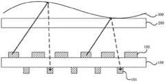
图1为现有技术提供的一种显示面板的结构示意图。参照图1,显示面板包括:相对设置的第一基板100和第二基板200,在第一基板100靠近第二基板200的一侧设置有发光单元102,在第一基板100远离第二基板200的一侧设置有指纹识别单元101。发光单元102作为指纹识别单元101的指纹识别光源。由发光单元102发出的光经触摸主体300反射后,入射到指纹识别单元101。指纹识别单元101通过检测反射光的强度,实现显示面板的指纹识别功能。此结构中,指纹识别单元101为外挂式指纹识别单元,其通过光学胶(图1中未示出)粘结于显示面板的第一基板100上,使得显示面板的整体厚度增加,不利于显示面板的轻薄化。FIG. 1 is a schematic structural diagram of a display panel provided in the prior art. Referring to FIG. 1 , the display panel includes: a
针对此问题,本发明实施例提供一种显示面板,以减少显示面板的整体厚度,从而实现显示面板的轻薄化。In response to this problem, embodiments of the present invention provide a display panel, so as to reduce the overall thickness of the display panel, so as to realize the lightness and thinness of the display panel.
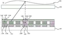
图2为本发明实施例提供的一种显示面板的结构示意图。参见图2,该显示面板01包括相对设置的第一基板100和第二基板200;第一基板100靠近第二基板200的一侧设置有多个发光单元110和多个指纹识别单元120,发光单元110包括第一N型半导体层110N和第一P型半导体层110P,指纹识别单元120包括第二N型半导体层120N和第二P型半导体层120P,第一N型半导体层110N和第二N型半导体层120N同层设置,第一P型半导体层110P和第二P型半导体层120P同层设置。FIG. 2 is a schematic structural diagram of a display panel according to an embodiment of the present invention. Referring to FIG. 2 , the
继续参见图2,第二N型半导体层120N和第二P型半导体层120P共同构成PN结。即指纹识别单元120本质上为光敏二极管,具有感光特性,并且具有单向导电性。无光照时,PN结有很小的饱和反向漏电流,即暗电流,此时PN结截止。当受到光照时,PN结的饱和反向漏电流大大增加,形成光电流,光电流随入射光强度的变化而变化,据此可以对触摸主体进行识别。Continuing to refer to FIG. 2 , the second N-
本发明实施例通过设置发光单元110的第一P型半导体层110P与指纹识别单元120的第二P型半导体层120P同层设置,发光单元110的第一N型半导体层110N与指纹识别单元120的第二N型半导体层120N同层设置,由此各发光单元和各指纹识别单元在第一基板所在平面上依次排列,而不是发光单元和各指纹识别单元在垂直于第一基板所在平面的方向上依次排列。即,无需在独立于发光单元110的膜层外单独设置指纹识别单元120,解决了现有的显示面板因采用外挂式的指纹识别单元,显示面板的整体厚度较厚,不利于实现显示面板的轻薄化的问题,实现了减少了显示面板的整体厚度,利于实现显示面板的轻薄化的目的。In the embodiment of the present invention, the first P-
可选地,第一N型半导体层110N和第二N型半导体层120N采用相同材料在同一制程中形成。与第一N型半导体层110N和第二N型半导体层120N分别于不同制程形成的方案相比,这样设置,在制作过程中只需一次刻蚀工艺,无需对第一N型半导体层110N和第二N型半导体层120N分别制作掩膜板,节省了成本,减少了制程数量,提高了生产效率。Optionally, the first N-
可选地,第一P型半导体层110P和第二P型半导体层120P采用相同材料在同一制程中形成。与第一P型半导体层110P和第二P型半导体层120P分别于不同制程形成的方案相比,这样设置,在制作过程中只需一次刻蚀工艺,无需对第一P型半导体层110P和第二P型半导体层120P分别制作掩膜板,节省了成本,减少了制程数量,提高了生产效率。Optionally, the first P-
需要说明的是,图2中,该显示面板包括两个重复单元,顺次相邻的3个发光单元110与1个指纹识别单元120构成一个重复单元。该显示面板共包括6个发光单元110和2个指纹识别单元120。这仅是本申请的一个具体示例,而非对本申请的限制。在实际中,显示面板中发光单元110和指纹识别单元120的数量和排列方式可根据实际需求设置。It should be noted that, in FIG. 2 , the display panel includes two repeating units, and three light-emitting
继续参见图2,发光单元110还包括层叠设置的阳极110A、第一发光层110E以及阴极110C;第一P型半导体层110P位于阳极110A和第一发光层110E之间;第一N型半导体层110N位于第一发光层110E和阴极110C之间;阳极110A位于第一基板100与第一发光层110E之间。Continuing to refer to FIG. 2 , the light-emitting
当进行图像显示时,向发光单元110的阳极110A和阴极110C施加驱动电压。在该驱动电压的作用下,在阴极110C和阳极110A之间会产生一个电场,进而促使电子从阴极110C向第一发光层110E传输,空穴则从阳极110A向第一发光层110E传输;电子和空穴在第一发光层110E中相遇,由于库仑力作用,电子和空穴被束缚在一起,形成处于激发态的激子。由于处于激发态的激子是不稳定的,它会将一部分能量传递给第一发光层110E中的发光分子,使发光分子中的电子从基态跃迁到激发态,而另一部分能量则以热或其他的形式释放,即能量损失。发光分子中处于激发态的电子不稳定,发生辐射跃迁,释放能量回到基态,此辐射跃迁过程中产生光子,即发光单元110发光。When image display is performed, a driving voltage is applied to the
其中,第一P型半导体层110P和第一N型半导体层110N可降低电子和空穴传输过程中的界面势垒,从而可提高发光单元中载流子(电子和空穴)注入能力,进而可提高发光单元110的发光效率。Among them, the first P-
继续参见图2,在上述技术方案中,设置阳极110A位于第一基板100与第一发光层110E之间,这仅是本申请的一个具体示例,而非对本申请的限制。可选地,还可以设置阴极110C位于第一基板100与第一发光层110E之间。Continuing to refer to FIG. 2 , in the above technical solution, the
在上述技术方案中,第一发光层110E的发光材料不同,与其对应的发光单元110发出的光的颜色可能不同。In the above technical solution, the light emitting material of the first
示例性的,第一发光层110E的材料可为红色发光材料、绿色发光材料或蓝色发光材料。Exemplarily, the material of the first light-emitting
继续参照图2,指纹识别单元120还可包括第一电极1201和第二电极1202;第一电极1201位于第二P型半导体层120P背离第二N型半导体层120N的一侧;第二电极1202位于第二N型半导体层120N背离第二P型半导体层120P的一侧。2, the
此时,指纹识别单元120的整体结构与有机光伏电池的结构类似,可利用光生载流子效应实现指纹识别功能。示例性的,指纹识别单元120采用光学指纹识别方式,由触摸主体300的指纹不同位置反射的光线入射到指纹识别单元120,指纹识别单元120接收指纹反射的光线,产生与指纹相关的电信号;由于指纹上存在凹凸变化的纹理,经由指纹不同位置反射的光线强度不同,最终使得不同指纹识别单元120接收到的光线的强度存在差别。而不同的光线强度下,电荷产生层(charge generation layer,CGL,包括第二P型半导体层120P和第二N型半导体层120N)反馈的电信号不同。从而可通过各指纹识别单元120反馈的电信号的大小反应触摸主体300的指纹特征,从而实现显示面板01的指纹识别功能。At this time, the overall structure of the
示例性的,电荷产生层反馈的电信号可包括电压信号或者电流信号。Exemplarily, the electrical signal fed back by the charge generation layer may include a voltage signal or a current signal.
示例性的,图2中,指纹识别单元120的第一电极1201是分立的,第二电极1202是连续的。这里“第二电极1202是连续”是指各个指纹识别单元120的第二电极1202彼此电连接,由此,可通过第一电极1201反馈电信号。Exemplarily, in FIG. 2 , the
需要说明的是,图2中仅示例性的示出了第一电极1201是分立的,第二电极1202是连续的,但并非对本实施例的限定。在其他实施方式中,可设置第一电极1201是连续的,第二电极1202是分立的;还可设置第一电极1201是分立的,第二电极1202也是分立的。It should be noted that, FIG. 2 only exemplarily shows that the
可选的,指纹识别单元120的第一电极1201与发光单元110的阳极110A同层设置,指纹识别单元120的第二电极1202与发光单元110的阴极110C同层设置。由此,各发光单元110和指纹识别单元120在第一基板所在平面上依次排列,而非在垂直于第一基板所在的平面上依次排列,即,无需在独立于发光单元110的膜层外,单独设置指纹识别单元120的第一电极1201和第二电极1202,从而可使显示面板01的整体厚度较薄,利于实现显示面板01的轻薄化。Optionally, the
可选的,第一电极1201与阳极110A采用相同的材料在同一制程中形成。与现有技术中第一电极1201和阳极110A分别在不同制程中形成的方案相比,这样设置,在制作过程中只需一次刻蚀工艺,无需对第一电极1201和阳极110A分别制作掩膜版,节省了成本,减少了制程数量,提高了生产效率。Optionally, the
可选的,第二电极1202和阴极110C采用相同的材料在同一制程中形成。与现有技术中第二电极1202和阴极110C分别在不同制程中形成的方案相比,这样设置,在制作过程中只需一次刻蚀工艺,无需对第二电极1202和阴极110C分别制作掩膜版,节省了成本,减少了制程数量,提高了生产效率。Optionally, the
图3为本发明实施例提供的另一种显示面板的结构示意图。与图2相比,图3中,该显示面板中,发光单元110还包括第一光学补偿层1101。参见图3,该第一光学补偿层1101位于第一发光层110E与阳极110A之间。该第一光学补偿层1101可选用空穴迁移率较高的材料,以提高空穴的注入或传输效率,进而提高显示面板的显示效果。可选地,第一光学补偿层1101可包括空穴注入层和/或空穴传输层。FIG. 3 is a schematic structural diagram of another display panel according to an embodiment of the present invention. Compared with FIG. 2 , in FIG. 3 , in the display panel, the
或者,还可以设置发光单元110还包括第二光学补偿层,该第二光学补偿层位于第一发光层110E与阴极110C之间(图3中未示出)。该第二光学补偿层可选用电子迁移率较高的材料,以提高电子的注入或传输效率,进而提高显示面板的显示效果。可选地,第二光学补偿层可包括电子注入层和/或电子传输层。Alternatively, the light-emitting
进一步地,还可以根据实际需要设置不同发光颜色的发光单元中,第一光学补偿层1101或者第二光学补偿层的厚度不同,以调节微腔效应,使得第一发光层110E的发光频率位于微腔内驻波场的增强锋附近。示例性的,第一发光层110E的发光频率与微腔驻波的波峰重合,或者第一发光层110E的发光频率与微腔驻波的波谷重合。Further, in light-emitting units with different light-emitting colors, the thickness of the first
图4为本发明实施例提供的又一种显示面板的结构示意图。参见图4,指纹识别单元120还可包括第二发光层120E;第二发光层120E位于第二P型半导体层120P和第二N型半导体层120N之间。FIG. 4 is a schematic structural diagram of another display panel according to an embodiment of the present invention. Referring to FIG. 4 , the
其中,指纹识别单元120的整体结构仍可视为有机光伏电池的结构,即仍可利用光生载流子效应实现指纹识别功能。The overall structure of the
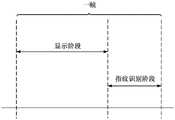
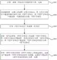
图5为本发明实施例提供的一种驱动周期的示意图。参照图5,显示面板01的工作过程可包括指纹识别阶段和显示阶段;在指纹识别阶段,指纹识别单元120用于进行指纹识别;在显示阶段,指纹识别单元120用于进行图像显示。FIG. 5 is a schematic diagram of a driving cycle provided by an embodiment of the present invention. 5, the working process of the
示例性的,显示面板还可以包括触控位置检测单元和/或触控压力检测单元,以及控制电路。当触控位置检测单元检测到触摸主体触摸时,控制显示面板处于指纹识别阶段,控制电路外向指纹识别单元120发送第一电信号,控制指纹识别单元120进行指纹识别;当触控位置检测单元未检测到触摸主体触摸时,控制显示面板处于显示阶段,控制电路向指纹识别单元120发送第二电信号,控制指纹识别单元120进行图像显示。图5示例性设置先进行显示,后进行指纹识别,但并非对本发明实施例提供的显示面板的限定。在其他实施方式中,还可以设置先进行指纹识别,后进行显示。Exemplarily, the display panel may further include a touch position detection unit and/or a touch pressure detection unit, and a control circuit. When the touch position detection unit detects that the touch subject is touched, the control display panel is in the fingerprint recognition stage, and the control circuit sends a first electrical signal to the
可选的,第二发光层120E的发光颜色可为红色、蓝色、绿色、白色、黄色或者橙色。Optionally, the light emission color of the second
其中,在显示阶段,第二发光层120E的发光颜色为白色时,指纹识别单元120用于显示面板01的亮度补偿;第二发光层120E的颜色为黄色或橙色时,指纹识别单元120用于显示面板01的色度补偿。In the display stage, when the light-emitting color of the second light-emitting
可选的,在显示阶段,还可根据需要显示的图像的不同,设置部分指纹识别单元120用来显示,剩余部分指纹识别单元120不工作,以保证显示面板具有较佳显示质量的同时,节省电能。Optionally, in the display stage, according to different images to be displayed, part of the
图6为本发明实施例提供的又一种显示面板的结构示意图。与图4相比,图6中,该显示面板01中,指纹识别单元120还可以包括第三光学补偿层1203。参见图6,该第三光学补偿层1203位于第二发光层120E和第一电极1201之间。该第三光学补偿层1203可选用空穴迁移率较高的材料,以提高空穴的传输或注入效率,进而提高显示面板的显示效果。可选的,第三光学补偿层1203可包括空穴注入层和/或空穴传输层。FIG. 6 is a schematic structural diagram of still another display panel according to an embodiment of the present invention. Compared with FIG. 4 , in FIG. 6 , in the
或者,还可以设置指纹识别单元120还包括第四光学补偿层,该第四光学补偿层位于发光层120E和第二电极1202之间(图6中未示出)。该第四光学补偿层可选用电子迁移率较高的材料,以提高电子的注入或传输效率,进而提高显示面板的显示效果。可选的,第四光学补偿层可包括电子注入层和/或电子传输层。Alternatively, the
进一步地,还可以根据实际需要设置不同发光颜色的发光单元中,第三光学补偿层1203或者第四光学补偿层的厚度不同,以调节微腔效应,使得第二发光层120E位于微腔内驻波场的增强锋附近。示例性的,第二发光层120E与微腔驻波的波峰重合,或者第二发光层120E与微腔驻波的波谷重合。Further, in light-emitting units with different light-emitting colors, the thicknesses of the third
可选的,图7为本发明实施例提供的又一种显示面板的结构示意图。参照图7,在同一显示面板01中,可设置部分指纹识别单元120的膜层结构包括第二发光层120E,部分指纹识别单元120的膜层结构不包括第二发光层120E。Optionally, FIG. 7 is a schematic structural diagram of another display panel according to an embodiment of the present invention. Referring to FIG. 7 , in the
在上述各实施例中,该显示面板还包括指纹识别光源。指纹识别光源发出的光线经由触摸主体反射后形成反射光入射到指纹识别单元,以进行指纹识别。在实际设置时,可以如图2-7所示,设置至少部分发光单元110作为指纹识别光源;发光单元110发出的光线经由触摸主体300反射后形成反射光入射到指纹识别单元120,以进行指纹识别。或者,在显示面板中设置外挂式指纹识别光源。In the above embodiments, the display panel further includes a fingerprint recognition light source. The light emitted by the fingerprint identification light source is reflected by the touch body to form reflected light and incident to the fingerprint identification unit for fingerprint identification. In the actual setting, as shown in FIGS. 2-7 , at least part of the light-emitting
其中,设置至少部分发光单元110作为指纹识别光源,不需要额外设置指纹识别光源,可进一步简化显示面板01的结构,降低显示面板的厚度以及制作难度。Wherein, at least part of the light-emitting
若在显示面板中设置外挂式指纹识别光源,可选地,指纹识别光源为红外光源。这样设置的好处是,红外光源与发光单元110发出的光线波段不同,可使显示面板01的图像显示功能和指纹识别功能不会相互影响,在提高显示面板01的图像显示质量的同时可提高指纹识别的精度。If an external fingerprint identification light source is provided in the display panel, optionally, the fingerprint identification light source is an infrared light source. The advantage of this arrangement is that the wavelengths of the light emitted by the infrared light source and the light-emitting
在上述技术方案的基础上,可选地,显示面板还可包括多个光线筛选结构。示例性地,继续参见图7,可选的,显示面板01还可包括多个光线筛选结构210,光线筛选结构210设置于第二基板200靠近第一基板100的一侧,指纹识别单元120在第一基板100上的垂直投影位于光线筛选结构210在第一基板100上的垂直投影内。On the basis of the above technical solutions, optionally, the display panel may further include a plurality of light screening structures. 7 , optionally, the
其中,光线筛管结构210包括多个与第二基板200表面垂直的光线筛选通道,与光线筛选通道平行的光线可通过光线筛选结构210,入射到指纹识别单元120;与光线筛选通道不平行的光线则被光线筛选结构210吸收,以避免由指纹识别光源出射,经触摸主体不同位置反射的光线照射至同一指纹识别单元120造成的串扰现象,提高指纹识别的准确性和精度。The light
需要说明的是,本发明实施例中仅示例性的示出了2个光线筛选结构210,但并非对本发明提供的显示面板01的限定。在其他实施方式中,光线筛选结构210的数量和位置可根据指纹识别单元120的数量和位置具体设置。It should be noted that, in the embodiment of the present invention, only two
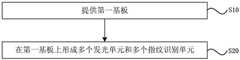
图8为本发明实施例提供的一种显示面板的制造方法的流程示意图。参照图8,该制造方法包括:FIG. 8 is a schematic flowchart of a method for manufacturing a display panel according to an embodiment of the present invention. 8, the manufacturing method includes:
S10、提供第一基板。S10. Provide a first substrate.
其中,第一基板可为刚性基板或柔性基板,本发明实施例对第一基板的材质不做具体限定。The first substrate may be a rigid substrate or a flexible substrate, and the material of the first substrate is not specifically limited in the embodiment of the present invention.
S20、在第一基板上形成多个发光单元和多个指纹识别单元。S20 , forming a plurality of light-emitting units and a plurality of fingerprint identification units on the first substrate.
其中,发光单元包括第一N型半导体层和第一P型半导体层,指纹识别单元包括第二N型半导体层和第二P型半导体层,第一N型半导体层和第二N型半导体层为同一膜层形成,第一P型半导体层和第二P型半导体层为同一膜层形成。The light-emitting unit includes a first N-type semiconductor layer and a first P-type semiconductor layer, the fingerprint identification unit includes a second N-type semiconductor layer and a second P-type semiconductor layer, the first N-type semiconductor layer and the second N-type semiconductor layer In order to form the same film layer, the first P-type semiconductor layer and the second P-type semiconductor layer are formed of the same film layer.
其中,P性半导体层和N型半导体层的形成方式可包括物理成膜方式或化学成膜方式,本发明实施例对此不限定。Wherein, the formation method of the P-type semiconductor layer and the N-type semiconductor layer may include a physical film formation method or a chemical film formation method, which is not limited in the embodiment of the present invention.
本发明实施例提供的显示面板的制造方法,通过设置发光单元的第一P型半导体层与指纹识别单元的第二P型半导体层同层设置,发光单元的第一N型半导体层与指纹之别单元的第二N型半导体层同层设置,由此各发光单元和各指纹识别单元在第一基板所在平面上依次排列,而非不是发光单元和各指纹识别单元在垂直与第一基板所在平面的方向上依次排列,即,无需在独立于发光单元的膜层外单独设置发光单元,解决了现有的显示面板因采用外挂式的指纹识别单元,显示面板的整体厚度较厚,不利于实现显示面板的轻薄化的问题,实现了减少了显示面板的整体厚度,利于实现显示面板的轻薄化的目的。In the manufacturing method of the display panel provided by the embodiment of the present invention, the first P-type semiconductor layer of the light-emitting unit and the second P-type semiconductor layer of the fingerprint identification unit are arranged in the same layer, and the first N-type semiconductor layer of the light-emitting unit and the fingerprint are arranged in the same layer. The second N-type semiconductor layers of other units are arranged in the same layer, so that each light-emitting unit and each fingerprint recognition unit are arranged in sequence on the plane where the first substrate is located, instead of the light-emitting unit and each fingerprint recognition unit being perpendicular to the first substrate. Arranged in sequence in the direction of the plane, that is, there is no need to separately arrange the light-emitting unit outside the film layer independent of the light-emitting unit, which solves the problem that the existing display panel adopts an external fingerprint identification unit, and the overall thickness of the display panel is thick, which is not conducive to The problem of realizing the lightness and thinness of the display panel is realized, and the overall thickness of the display panel is reduced, which is beneficial to the purpose of realizing the lightness and thinness of the display panel.
图9为本发明实施例提供的另一种显示面板的制造方法的流程示意图,是对图8中步骤S20的示例性说明。参照图9,在第一基板上形成多个发光单元和多个指纹识别单元,可包括:FIG. 9 is a schematic flowchart of another method for manufacturing a display panel according to an embodiment of the present invention, which is an exemplary illustration of step S20 in FIG. 8 . Referring to FIG. 9 , a plurality of light-emitting units and a plurality of fingerprint identification units are formed on the first substrate, which may include:
S201、在第一基板上形成多个阳极和多个第一电极。S201 , forming a plurality of anodes and a plurality of first electrodes on a first substrate.
示例性的,发光单元的阳极和指纹识别单元的第一电极采用相同的材料,在同一制程中形成。与现有技术中阳极和第一电极的分别在不同制程中形成的方案相比而言,这样设置,在制作过程中只需一次蒸镀工艺,无需对第一电极和阳极分别制作掩膜版,节省了成本,减少了制程数量,提高了生产效率。Exemplarily, the anode of the light-emitting unit and the first electrode of the fingerprint identification unit are made of the same material and formed in the same process. Compared with the solution in the prior art in which the anode and the first electrode are formed in different manufacturing processes, this arrangement requires only one evaporation process during the manufacturing process, and there is no need to separately make masks for the first electrode and the anode. , saving costs, reducing the number of processes, and improving production efficiency.
S202、在阳极和第一电极上形成第三P型半导体层,第三P型半导体层中覆盖阳极的部分为第一P型半导体层,第三P型半导体层中覆盖第一电极的部分为第二P型半导体层。S202, forming a third P-type semiconductor layer on the anode and the first electrode, the part of the third P-type semiconductor layer covering the anode is the first P-type semiconductor layer, and the part of the third P-type semiconductor layer covering the first electrode is The second P-type semiconductor layer.
示例性的,发光单元的第一P型半导体层和指纹识别单元的第二P型半导体层采用相同的材料在同一制程中形成。与第一P型半导体层和第二P型半导体层分别于不同制程形成的方案相比,这样设置,在制作过程中只需一次刻蚀工艺,无需对第一P型半导体层和第二P型半导体层分别制作掩膜板,节省了成本,减少了制程数量,提高了生产效率。Exemplarily, the first P-type semiconductor layer of the light-emitting unit and the second P-type semiconductor layer of the fingerprint identification unit are formed in the same process using the same material. Compared with the solution in which the first P-type semiconductor layer and the second P-type semiconductor layer are formed in different processes, this arrangement requires only one etching process during the production process, and does not need to perform the first P-type semiconductor layer and the second P-type semiconductor layer. The mask plates are separately made from the type semiconductor layers, which saves the cost, reduces the number of manufacturing processes, and improves the production efficiency.
S203、在第一P型半导体层上形成第一发光层。S203, forming a first light-emitting layer on the first P-type semiconductor layer.
示例性的,第一发光层的发光材料不同,与其对应的发光单元发出的光的颜色可能不同。Exemplarily, if the light-emitting material of the first light-emitting layer is different, the color of the light emitted by the corresponding light-emitting unit may be different.
S204、在第一发光层和第二P型半导体层上形成第三N型半导体层,第三N型半导体层中覆盖第一发光层的部分为第一N型半导体层,第三N型半导体层中覆盖第二P型半导体层的部分为第二N型半导体层。S204, forming a third N-type semiconductor layer on the first light-emitting layer and the second P-type semiconductor layer, the part of the third N-type semiconductor layer covering the first light-emitting layer is the first N-type semiconductor layer, and the third N-type semiconductor layer The part of the layer covering the second P-type semiconductor layer is the second N-type semiconductor layer.
示例性的,发光单元的第一N型半导体层和指纹识别单元的第二N型半导体层采用相同的材料在同一制程中形成。与第一N型半导体层和第二N型半导体层分别于不同制程形成的方案相比,这样设置,在制作过程中只需一次刻蚀工艺,无需对第一N型半导体层和第二N型半导体层分别制作掩膜板,节省了成本,减少了制程数量,提高了生产效率。Exemplarily, the first N-type semiconductor layer of the light-emitting unit and the second N-type semiconductor layer of the fingerprint identification unit are formed in the same process using the same material. Compared with the scheme in which the first N-type semiconductor layer and the second N-type semiconductor layer are formed in different processes, this arrangement requires only one etching process during the production process, and does not need to perform the first N-type semiconductor layer and the second N-type semiconductor layer. The mask plates are separately made from the type semiconductor layers, which saves the cost, reduces the number of manufacturing processes, and improves the production efficiency.
需要说明的是,本发明实施例对P型半导体层和N型半导体层的具体材质和具体形成方式不做限定。It should be noted that the embodiments of the present invention do not limit the specific materials and specific formation methods of the P-type semiconductor layer and the N-type semiconductor layer.
S205、在第一N型半导体层和第二N型半导体层上形成金属层,金属层覆盖第一N型半导体层的部分为阴极,金属层覆盖第二N型半导体层的部分为第二电极。S205, forming a metal layer on the first N-type semiconductor layer and the second N-type semiconductor layer, the part of the metal layer covering the first N-type semiconductor layer is the cathode, and the part of the metal layer covering the second N-type semiconductor layer is the second electrode .
示例性的,发光单元的阴极和指纹识别单元的第二电极采用相同的材料在同一制程中形成。与现有技术中第二电极和阴极分别在不同制程中形成的方案相比,这样设置,在制作过程中只需一次刻蚀工艺,无需对第二电极和阴极分别制作掩膜版,节省了成本,减少了制程数量,提高了生产效率。。Exemplarily, the cathode of the light-emitting unit and the second electrode of the fingerprint identification unit are formed using the same material in the same process. Compared with the solution in the prior art in which the second electrode and the cathode are formed in different manufacturing processes, this arrangement requires only one etching process during the manufacturing process, and there is no need to separately make masks for the second electrode and the cathode, which saves money. cost, reduce the number of processes, and improve production efficiency. .
示例性的,金属层的材料可为金、银、铜等金属导电材料,金属层的形成方式可为物理成膜方式或化学成膜方式,本发明实施例对金属层的具体材质和具体形成方式不做限定。Exemplarily, the material of the metal layer can be a metal conductive material such as gold, silver, copper, etc., and the formation method of the metal layer can be a physical film-forming method or a chemical film-forming method. The method is not limited.
本发明实施例提供的显示面板的制造方法,通过设置指纹识别单元的第一电极和发光单元的阳极在同一制程中形成,指纹识别单元的第二N型半导体层和发光单元的第一N型半导体层在同一制程中形成,指纹识别单元的第二P型半导体层和发光单元的第一P型半导体层在同一制程中形成,指纹识别单元的第二电极和发光单元的阴极在同一制程中形成,由此各发光单元和各指纹识别单元在第一基板所在平面上依次排列,而不是发光单元和各指纹识别单元在垂直与第一基板所在平面的方向上依次排列,即,无需在独立于发光单元的膜层外单独设置发光单元,解决了现有的显示面板因采用外挂式的指纹识别单元,显示面板的整体厚度较厚,不利于实现显示面板的轻薄化的问题,实现了减少了显示面板的整体厚度,利于实现显示面板的轻薄化的目的。同时,无需针对发光单元和指纹识别单元的每一膜层分别制作掩膜版,节省了成本,减少了制程数量,提供了生产效率。In the manufacturing method of the display panel provided by the embodiment of the present invention, the first electrode of the fingerprint identification unit and the anode of the light-emitting unit are formed in the same process, and the second N-type semiconductor layer of the fingerprint identification unit and the first N-type of the light-emitting unit are formed in the same process. The semiconductor layer is formed in the same process, the second P-type semiconductor layer of the fingerprint recognition unit and the first P-type semiconductor layer of the light-emitting unit are formed in the same process, and the second electrode of the fingerprint recognition unit and the cathode of the light-emitting unit are formed in the same process. Thus, each light-emitting unit and each fingerprint recognition unit are arranged in sequence on the plane where the first substrate is located, instead of the light-emitting unit and each fingerprint recognition unit being sequentially arranged in the direction perpendicular to the plane where the first substrate is located, that is, there is no need to independently The light-emitting unit is separately arranged outside the film layer of the light-emitting unit, which solves the problem that the overall thickness of the display panel is relatively thick due to the use of an external fingerprint identification unit in the existing display panel, which is not conducive to realizing the lightness and thinness of the display panel. The overall thickness of the display panel is reduced, which is beneficial to realize the purpose of lightening and thinning the display panel. At the same time, there is no need to separately make masks for each film layer of the light-emitting unit and the fingerprint identification unit, which saves costs, reduces the number of manufacturing processes, and improves production efficiency.
图10为本发明实施例提供的又一种显示面板的制造方法的流程示意图,是对图8中步骤S20的又一示例性说明。参照图10,在第一基板上形成多个发光单元和多个指纹识别单元,可包括:FIG. 10 is a schematic flowchart of another method for manufacturing a display panel according to an embodiment of the present invention, which is another exemplary illustration of step S20 in FIG. 8 . Referring to FIG. 10 , a plurality of light-emitting units and a plurality of fingerprint identification units are formed on the first substrate, which may include:
S301、在第一基板上形成多个阳极和多个第一电极。S301 , forming a plurality of anodes and a plurality of first electrodes on a first substrate.
S302、在阳极和第一电极上形成第三P型半导体层,第三P型半导体层中覆盖阳极的部分为第一P型半导体层,第三P型半导体层中覆盖第一电极的部分为第二P型半导体层。S302, forming a third P-type semiconductor layer on the anode and the first electrode, the part of the third P-type semiconductor layer covering the anode is the first P-type semiconductor layer, and the part of the third P-type semiconductor layer covering the first electrode is The second P-type semiconductor layer.
S303、在第一P型半导体层上形成第一发光层。用于形成显示面板的发光单元。S303 , forming a first light-emitting layer on the first P-type semiconductor layer. A light emitting unit for forming a display panel.
S304、在第二P型半导体层上形成第二发光层。用于形成显示面板的指纹识别单元。S304 , forming a second light-emitting layer on the second P-type semiconductor layer. A fingerprint recognition unit for forming a display panel.
其中,第二发光层的发光颜色可为红色、绿色、蓝色、白色、黄色或者橙色。Wherein, the light-emitting color of the second light-emitting layer may be red, green, blue, white, yellow or orange.
S305、在第一发光层和第二发光层上形成第三N型半导体层,第三N型半导体层中覆盖第一发光层的部分为第一N型半导体层,第三N型半导体层中覆盖第二发光层的部分为第二N型半导体层。S305. A third N-type semiconductor layer is formed on the first light-emitting layer and the second light-emitting layer. The part of the third N-type semiconductor layer covering the first light-emitting layer is the first N-type semiconductor layer, and the third N-type semiconductor layer is the first N-type semiconductor layer. The part covering the second light-emitting layer is the second N-type semiconductor layer.
S306、在第一N型半导体层和第二N型半导体层上形成金属层,金属层覆盖第一N型半导体层的部分为阴极,金属层覆盖第二N型半导体层的部分为第二电极。S306, forming a metal layer on the first N-type semiconductor layer and the second N-type semiconductor layer, the part of the metal layer covering the first N-type semiconductor layer is the cathode, and the part of the metal layer covering the second N-type semiconductor layer is the second electrode .
本发明实施例提供的显示面板的制造方法,通过设置指纹识别单元的第一电极和发光单元的阳极在同一制程中形成,指纹识别单元的第二N型半导体层和发光单元的第一N型半导体层在同一制程中形成,指纹识别单元的第二P型半导体层和发光单元的第一P型半导体层在同一制程中形成,指纹识别单元的第二电极和发光单元的阴极在同一制程中形成,由此,一方面,各发光单元和各指纹识别单元在第一基板所在平面上依次排列,而不是发光单元和各指纹识别单元在垂直与第一基板所在平面的方向上依次排列,即,无需在独立于发光单元的膜层外单独设置发光单元,解决了现有的显示面板因采用外挂式的指纹识别单元,显示面板的整体厚度较厚,不利于实现显示面板的轻薄化的问题,实现了减少了显示面板的整体厚度,利于实现显示面板的轻薄化的目的。另一方面,无需针对发光单元和指纹识别单元的每一膜层分别制作掩膜版,节省了成本,减少了制程数量,提供了生产效率。又一方面,本发明实施例提供的指纹识别单元还包括第二发光层,可实现指纹识别单元的分时复用,提高显示面板的图像显示效果。In the manufacturing method of the display panel provided by the embodiment of the present invention, the first electrode of the fingerprint identification unit and the anode of the light-emitting unit are formed in the same process, and the second N-type semiconductor layer of the fingerprint identification unit and the first N-type of the light-emitting unit are formed in the same process. The semiconductor layer is formed in the same process, the second P-type semiconductor layer of the fingerprint recognition unit and the first P-type semiconductor layer of the light-emitting unit are formed in the same process, and the second electrode of the fingerprint recognition unit and the cathode of the light-emitting unit are formed in the same process. Thus, on the one hand, each light-emitting unit and each fingerprint recognition unit are arranged in sequence on the plane where the first substrate is located, rather than the light-emitting unit and each fingerprint recognition unit are sequentially arranged in the direction perpendicular to the plane where the first substrate is located, that is, , there is no need to set a light-emitting unit outside the film layer independent of the light-emitting unit, which solves the problem that the existing display panel adopts an external fingerprint identification unit, and the overall thickness of the display panel is relatively thick, which is not conducive to realizing the thinning of the display panel. , the overall thickness of the display panel is reduced, and the purpose of realizing the lightness and thinness of the display panel is achieved. On the other hand, there is no need to separately make masks for each film layer of the light-emitting unit and the fingerprint identification unit, which saves costs, reduces the number of manufacturing processes, and improves production efficiency. In another aspect, the fingerprint identification unit provided by the embodiment of the present invention further includes a second light-emitting layer, which can realize time-division multiplexing of the fingerprint identification unit and improve the image display effect of the display panel.
图11为本发明实施例提供的又一种显示面板的制造方法的流程示意图。参照图11,在图8-图10任一图的基础上,显示面板的制造方法还包括:FIG. 11 is a schematic flowchart of another method for manufacturing a display panel according to an embodiment of the present invention. Referring to FIG. 11 , on the basis of any one of FIGS. 8 to 10 , the manufacturing method of the display panel further includes:
S40、提供第二基板。S40, providing a second substrate.
其中,第二基板可为刚性基板或柔性基板,本发明实施例对第二基板的材质不做具体限定。The second substrate may be a rigid substrate or a flexible substrate, and the material of the second substrate is not specifically limited in the embodiment of the present invention.
S50、在第二基板上形成多个光线筛选结构。S50, forming a plurality of light screening structures on the second substrate.
其中,光线筛选结构用于吸收与第二基板表面不垂直的光线,只允许与第二基板表面垂直的光线透过。本发明实施例对光线筛选结构的具体材质和具体形成方式不做特殊限定。Wherein, the light screening structure is used for absorbing light not perpendicular to the surface of the second substrate, and only allowing the light perpendicular to the surface of the second substrate to pass through. The embodiments of the present invention do not specifically limit the specific material and specific formation method of the light screening structure.
S60、将第一基板和第二基板对位贴合,以使指纹识别单元在第一基板上的垂直投影位于光线筛选结构在第一基板上的垂直投影内,且多个光线筛选结构位于第二基板靠近第一基板的一侧,发光单元和指纹识别单元位于第一基板靠近第二基板的一侧。S60. Align the first substrate and the second substrate, so that the vertical projection of the fingerprint identification unit on the first substrate is within the vertical projection of the light screening structure on the first substrate, and the plurality of light screening structures are positioned on the first substrate. The second substrate is close to one side of the first substrate, and the light-emitting unit and the fingerprint identification unit are located on the side of the first substrate close to the second substrate.
这样设置,可以避免由指纹识别光源出射,经触摸主体不同位置反射的光线照射至同一指纹识别单元120造成的串扰现象,提高指纹识别的准确性和精度。This arrangement can avoid the crosstalk phenomenon caused by the light reflected from different positions of the touch subject radiating from the fingerprint identification light source to the same
本发明实施例还提供了一种显示装置,示例性的,图12为本发明实施例提供的一种显示装置的结构示意图。参照图12,该显示装置02包括上述显示面板01。An embodiment of the present invention further provides a display device. By way of example, FIG. 12 is a schematic structural diagram of a display device provided by an embodiment of the present invention. Referring to FIG. 12 , the
示例性的,显示装置02可以包括手机、电脑以及智能可穿戴设备等显示装置,本发明实施例对此不作特殊限定。Exemplarily, the
本实施例提供的显示装置,通过设置显示面板中发光单元的第一N型半导体层和指纹识别单元的第二N型半导体层同层设置,发光单元的第一P型半导体层和指纹识别单元的第二P型半导体层同层设置,由此各发光单元和各指纹识别单元在第一基板所在平面上依次排列,而不是发光单元和各指纹识别单元在垂直与第一基板所在平面的方向上依次排列,即,无需在独立于发光单元110的膜层外单独设置发光单元120,解决了现有的显示面板因采用外挂式的指纹识别单元,显示面板的整体厚度较厚,不利于实现显示面板的轻薄化的问题,实现了减少了显示面板的整体厚度,利于实现显示面板的轻薄化的目的。。In the display device provided by this embodiment, the first N-type semiconductor layer of the light-emitting unit in the display panel and the second N-type semiconductor layer of the fingerprint identification unit are arranged in the same layer, and the first P-type semiconductor layer of the light-emitting unit and the fingerprint identification unit are arranged in the same layer. The second P-type semiconductor layer is arranged in the same layer, so that each light-emitting unit and each fingerprint recognition unit are arranged in sequence on the plane where the first substrate is located, instead of the light-emitting unit and each fingerprint recognition unit in the direction perpendicular to the plane where the first substrate is located That is, the light-emitting
注意,上述仅为本发明的较佳实施例及所运用技术原理。本领域技术人员会理解,本发明不限于这里所述的特定实施例,对本领域技术人员来说能够进行各种明显的变化、重新调整、相互结合和替代而不会脱离本发明的保护范围。因此,虽然通过以上实施例对本发明进行了较为详细的说明,但是本发明不仅仅限于以上实施例,在不脱离本发明构思的情况下,还可以包括更多其他等效实施例,而本发明的范围由所附的权利要求范围决定。Note that the above are only preferred embodiments of the present invention and applied technical principles. Those skilled in the art will understand that the present invention is not limited to the specific embodiments described herein, and various obvious changes, readjustments, combinations and substitutions can be made by those skilled in the art without departing from the protection scope of the present invention. Therefore, although the present invention has been described in detail through the above embodiments, the present invention is not limited to the above embodiments, and can also include more other equivalent embodiments without departing from the concept of the present invention. The scope is determined by the scope of the appended claims.
Claims (12)
Translated fromChinesePriority Applications (2)
| Application Number | Priority Date | Filing Date | Title |
|---|---|---|---|
| CN201810201260.3ACN108493201B (en) | 2018-03-12 | 2018-03-12 | A display panel, its manufacturing method and display device |
| US16/175,997US10522584B2 (en) | 2018-03-12 | 2018-10-31 | Display panel, manufacturing method thereof and display device |
Applications Claiming Priority (1)
| Application Number | Priority Date | Filing Date | Title |
|---|---|---|---|
| CN201810201260.3ACN108493201B (en) | 2018-03-12 | 2018-03-12 | A display panel, its manufacturing method and display device |
Publications (2)
| Publication Number | Publication Date |
|---|---|
| CN108493201A CN108493201A (en) | 2018-09-04 |
| CN108493201Btrue CN108493201B (en) | 2020-10-16 |
Family
ID=63338901
Family Applications (1)
| Application Number | Title | Priority Date | Filing Date |
|---|---|---|---|
| CN201810201260.3AActiveCN108493201B (en) | 2018-03-12 | 2018-03-12 | A display panel, its manufacturing method and display device |
Country Status (2)
| Country | Link |
|---|---|
| US (1) | US10522584B2 (en) |
| CN (1) | CN108493201B (en) |
Families Citing this family (6)
| Publication number | Priority date | Publication date | Assignee | Title |
|---|---|---|---|---|
| KR102589620B1 (en)* | 2018-10-29 | 2023-10-17 | 삼성전자주식회사 | Display device and method of fabricating the same |
| CN109886163B (en)* | 2019-01-30 | 2021-08-06 | 武汉华星光电半导体显示技术有限公司 | Display device with fingerprint recognition function and manufacturing method thereof |
| EP4022674A2 (en)* | 2019-08-26 | 2022-07-06 | X-Celeprint Limited | Variable stiffness modules |
| CN110931533B (en)* | 2019-12-10 | 2022-11-25 | 武汉天马微电子有限公司 | Display panel, manufacturing method thereof and display device |
| CN112257524B (en)* | 2020-10-09 | 2023-11-03 | 武汉华星光电半导体显示技术有限公司 | Fingerprint identification display panel and fingerprint identification display device |
| JPWO2023017352A1 (en)* | 2021-08-11 | 2023-02-16 |
Citations (5)
| Publication number | Priority date | Publication date | Assignee | Title |
|---|---|---|---|---|
| CN1735298A (en)* | 2004-08-04 | 2006-02-15 | 株式会社半导体能源研究所 | Light emitting elements, display devices and electronic appliances |
| CN103022072A (en)* | 2011-09-26 | 2013-04-03 | 株式会社东芝 | Photoelectric conversion device and manufacturing method thereof |
| CN105047689A (en)* | 2015-08-12 | 2015-11-11 | 京东方科技集团股份有限公司 | Organic light-emitting diode display substrate and light reflection surface structure identification method thereof |
| CN106229331A (en)* | 2016-08-31 | 2016-12-14 | 上海箩箕技术有限公司 | Self-luminous display pixel |
| CN106897699A (en)* | 2017-02-24 | 2017-06-27 | 京东方科技集团股份有限公司 | A kind of fingerprint recognition device, OLED display |
Family Cites Families (9)
| Publication number | Priority date | Publication date | Assignee | Title |
|---|---|---|---|---|
| FR2850190B1 (en)* | 2003-01-21 | 2006-04-28 | Atmel Grenoble Sa | METHOD AND DEVICE FOR RECOGNIZING PERSON |
| JP2006295104A (en)* | 2004-07-23 | 2006-10-26 | Semiconductor Energy Lab Co Ltd | LIGHT EMITTING ELEMENT AND LIGHT EMITTING DEVICE USING THE SAME |
| US20090141004A1 (en)* | 2007-12-03 | 2009-06-04 | Semiconductor Energy Laboratory Co., Ltd. | Display device and method for manufacturing the same |
| KR101404919B1 (en) | 2011-11-08 | 2014-06-13 | 건국대학교 산학협력단 | Poly-thiophene based organic photovoltaic devices with conducting additive and manufacturing method for the same |
| TWI685961B (en)* | 2016-06-17 | 2020-02-21 | 優顯科技股份有限公司 | Optoelectronic semiconductor device |
| CN106873063B (en) | 2017-02-23 | 2018-09-18 | 京东方科技集团股份有限公司 | A kind of display device |
| WO2018210317A1 (en)* | 2017-05-17 | 2018-11-22 | Shenzhen GOODIX Technology Co., Ltd. | Optical fingerprint sensor with non-touch imaging capability |
| US10664684B2 (en)* | 2017-06-02 | 2020-05-26 | Next Biometrics Group Asa | Fingerprint sensor with liveness detection |
| CN107506728B (en)* | 2017-08-23 | 2021-02-12 | 京东方科技集团股份有限公司 | Photosensitive unit, photosensitive module and photosensitive device |
- 2018
- 2018-03-12CNCN201810201260.3Apatent/CN108493201B/enactiveActive
- 2018-10-31USUS16/175,997patent/US10522584B2/enactiveActive
Patent Citations (5)
| Publication number | Priority date | Publication date | Assignee | Title |
|---|---|---|---|---|
| CN1735298A (en)* | 2004-08-04 | 2006-02-15 | 株式会社半导体能源研究所 | Light emitting elements, display devices and electronic appliances |
| CN103022072A (en)* | 2011-09-26 | 2013-04-03 | 株式会社东芝 | Photoelectric conversion device and manufacturing method thereof |
| CN105047689A (en)* | 2015-08-12 | 2015-11-11 | 京东方科技集团股份有限公司 | Organic light-emitting diode display substrate and light reflection surface structure identification method thereof |
| CN106229331A (en)* | 2016-08-31 | 2016-12-14 | 上海箩箕技术有限公司 | Self-luminous display pixel |
| CN106897699A (en)* | 2017-02-24 | 2017-06-27 | 京东方科技集团股份有限公司 | A kind of fingerprint recognition device, OLED display |
Also Published As
| Publication number | Publication date |
|---|---|
| CN108493201A (en) | 2018-09-04 |
| US20190280040A1 (en) | 2019-09-12 |
| US10522584B2 (en) | 2019-12-31 |
Similar Documents
| Publication | Publication Date | Title |
|---|---|---|
| CN108493201B (en) | A display panel, its manufacturing method and display device | |
| CN108258024B (en) | Display panel and display device | |
| CN110931522B (en) | Display panel and manufacturing method thereof | |
| CN108491801B (en) | Display panel and display device | |
| CN105243361B (en) | Optical detection device and manufacturing method thereof | |
| JP5769724B2 (en) | Method and apparatus for sensing infrared radiation | |
| CN110767739A (en) | Display substrate and display device | |
| CN108075048B (en) | OLED panel, manufacturing method thereof and display device | |
| JP2017103254A (en) | Light emitting device | |
| WO2015143838A1 (en) | Oled pixel structure and manufacturing method therefor, oled display panel and oled display | |
| CN113555509B (en) | Display device and display panel | |
| WO2021253558A1 (en) | Display panel and preparation method therefor, and display apparatus | |
| CN106684113A (en) | Organic luminescent display panel, device and manufacturing method thereof | |
| CN109166901B (en) | OLED display substrate, display device and manufacturing method thereof | |
| CN110047902A (en) | The production method and display device of a kind of organic electroluminescence device, display panel | |
| CN110890411A (en) | A display panel and display device | |
| CN108962958B (en) | Display panel, display device and manufacturing method of display panel | |
| CN112885883B (en) | Display screen, manufacturing method of display screen, and electronic device | |
| CN109768074B (en) | Display substrate, manufacturing method thereof, display panel and display device | |
| CN111987131A (en) | A display panel, its manufacturing method, and display device | |
| US20230096622A1 (en) | Electronic device and method of measuring biometric information using same | |
| CN112270248B (en) | Preparation method of optical fingerprint sensor, optical fingerprint sensor and display screen | |
| CN105280830A (en) | Organic light emitting device and manufacturing method thereof and display device | |
| CN115707295A (en) | Display device | |
| TW202247457A (en) | Laminate for image display device and image display device |
Legal Events
| Date | Code | Title | Description |
|---|---|---|---|
| PB01 | Publication | ||
| PB01 | Publication | ||
| SE01 | Entry into force of request for substantive examination | ||
| SE01 | Entry into force of request for substantive examination | ||
| GR01 | Patent grant | ||
| GR01 | Patent grant | ||
| TR01 | Transfer of patent right | Effective date of registration:20211103 Address after:No.8, liufangyuan Henglu, Donghu New Technology Development Zone, Wuhan City, Hubei Province Patentee after:WUHAN TIANMA MICROELECTRONICS Co.,Ltd. Patentee after:Wuhan Tianma Microelectronics Co.,Ltd. Shanghai Branch Address before:Room 509, building 1, No. 6111, Longdong Avenue, Pudong New Area, Shanghai, 200120 Patentee before:SHANGHAI TIANMA AM-OLED Co.,Ltd. | |
| TR01 | Transfer of patent right |